WO2011135973A1 - バックライトユニットおよび液晶表示装置 - Google Patents
バックライトユニットおよび液晶表示装置 Download PDFInfo
- Publication number
- WO2011135973A1 WO2011135973A1 PCT/JP2011/058268 JP2011058268W WO2011135973A1 WO 2011135973 A1 WO2011135973 A1 WO 2011135973A1 JP 2011058268 W JP2011058268 W JP 2011058268W WO 2011135973 A1 WO2011135973 A1 WO 2011135973A1
- Authority
- WO
- WIPO (PCT)
- Prior art keywords
- chassis
- backlight unit
- led
- aluminum
- light source
- Prior art date
- Legal status (The legal status is an assumption and is not a legal conclusion. Google has not performed a legal analysis and makes no representation as to the accuracy of the status listed.)
- Ceased
Links
Images









Classifications
-
- G—PHYSICS
- G02—OPTICS
- G02F—OPTICAL DEVICES OR ARRANGEMENTS FOR THE CONTROL OF LIGHT BY MODIFICATION OF THE OPTICAL PROPERTIES OF THE MEDIA OF THE ELEMENTS INVOLVED THEREIN; NON-LINEAR OPTICS; FREQUENCY-CHANGING OF LIGHT; OPTICAL LOGIC ELEMENTS; OPTICAL ANALOGUE/DIGITAL CONVERTERS
- G02F1/00—Devices or arrangements for the control of the intensity, colour, phase, polarisation or direction of light arriving from an independent light source, e.g. switching, gating or modulating; Non-linear optics
- G02F1/01—Devices or arrangements for the control of the intensity, colour, phase, polarisation or direction of light arriving from an independent light source, e.g. switching, gating or modulating; Non-linear optics for the control of the intensity, phase, polarisation or colour
- G02F1/13—Devices or arrangements for the control of the intensity, colour, phase, polarisation or direction of light arriving from an independent light source, e.g. switching, gating or modulating; Non-linear optics for the control of the intensity, phase, polarisation or colour based on liquid crystals, e.g. single liquid crystal display cells
- G02F1/133—Constructional arrangements; Operation of liquid crystal cells; Circuit arrangements
- G02F1/1333—Constructional arrangements; Manufacturing methods
- G02F1/1335—Structural association of cells with optical devices, e.g. polarisers or reflectors
- G02F1/1336—Illuminating devices
- G02F1/133602—Direct backlight
- G02F1/133603—Direct backlight with LEDs
-
- G—PHYSICS
- G02—OPTICS
- G02F—OPTICAL DEVICES OR ARRANGEMENTS FOR THE CONTROL OF LIGHT BY MODIFICATION OF THE OPTICAL PROPERTIES OF THE MEDIA OF THE ELEMENTS INVOLVED THEREIN; NON-LINEAR OPTICS; FREQUENCY-CHANGING OF LIGHT; OPTICAL LOGIC ELEMENTS; OPTICAL ANALOGUE/DIGITAL CONVERTERS
- G02F1/00—Devices or arrangements for the control of the intensity, colour, phase, polarisation or direction of light arriving from an independent light source, e.g. switching, gating or modulating; Non-linear optics
- G02F1/01—Devices or arrangements for the control of the intensity, colour, phase, polarisation or direction of light arriving from an independent light source, e.g. switching, gating or modulating; Non-linear optics for the control of the intensity, phase, polarisation or colour
- G02F1/13—Devices or arrangements for the control of the intensity, colour, phase, polarisation or direction of light arriving from an independent light source, e.g. switching, gating or modulating; Non-linear optics for the control of the intensity, phase, polarisation or colour based on liquid crystals, e.g. single liquid crystal display cells
- G02F1/133—Constructional arrangements; Operation of liquid crystal cells; Circuit arrangements
- G02F1/1333—Constructional arrangements; Manufacturing methods
- G02F1/133308—Support structures for LCD panels, e.g. frames or bezels
- G02F1/133314—Back frames
-
- G—PHYSICS
- G02—OPTICS
- G02F—OPTICAL DEVICES OR ARRANGEMENTS FOR THE CONTROL OF LIGHT BY MODIFICATION OF THE OPTICAL PROPERTIES OF THE MEDIA OF THE ELEMENTS INVOLVED THEREIN; NON-LINEAR OPTICS; FREQUENCY-CHANGING OF LIGHT; OPTICAL LOGIC ELEMENTS; OPTICAL ANALOGUE/DIGITAL CONVERTERS
- G02F1/00—Devices or arrangements for the control of the intensity, colour, phase, polarisation or direction of light arriving from an independent light source, e.g. switching, gating or modulating; Non-linear optics
- G02F1/01—Devices or arrangements for the control of the intensity, colour, phase, polarisation or direction of light arriving from an independent light source, e.g. switching, gating or modulating; Non-linear optics for the control of the intensity, phase, polarisation or colour
- G02F1/13—Devices or arrangements for the control of the intensity, colour, phase, polarisation or direction of light arriving from an independent light source, e.g. switching, gating or modulating; Non-linear optics for the control of the intensity, phase, polarisation or colour based on liquid crystals, e.g. single liquid crystal display cells
- G02F1/133—Constructional arrangements; Operation of liquid crystal cells; Circuit arrangements
- G02F1/1333—Constructional arrangements; Manufacturing methods
- G02F1/1335—Structural association of cells with optical devices, e.g. polarisers or reflectors
- G02F1/1336—Illuminating devices
- G02F1/133628—Illuminating devices with cooling means
-
- H—ELECTRICITY
- H01—ELECTRIC ELEMENTS
- H01M—PROCESSES OR MEANS, e.g. BATTERIES, FOR THE DIRECT CONVERSION OF CHEMICAL ENERGY INTO ELECTRICAL ENERGY
- H01M4/00—Electrodes
- H01M4/02—Electrodes composed of, or comprising, active material
- H01M4/04—Processes of manufacture in general
- H01M4/0438—Processes of manufacture in general by electrochemical processing
- H01M4/044—Activating, forming or electrochemical attack of the supporting material
- H01M4/0442—Anodisation, Oxidation
-
- Y—GENERAL TAGGING OF NEW TECHNOLOGICAL DEVELOPMENTS; GENERAL TAGGING OF CROSS-SECTIONAL TECHNOLOGIES SPANNING OVER SEVERAL SECTIONS OF THE IPC; TECHNICAL SUBJECTS COVERED BY FORMER USPC CROSS-REFERENCE ART COLLECTIONS [XRACs] AND DIGESTS
- Y02—TECHNOLOGIES OR APPLICATIONS FOR MITIGATION OR ADAPTATION AGAINST CLIMATE CHANGE
- Y02E—REDUCTION OF GREENHOUSE GAS [GHG] EMISSIONS, RELATED TO ENERGY GENERATION, TRANSMISSION OR DISTRIBUTION
- Y02E60/00—Enabling technologies; Technologies with a potential or indirect contribution to GHG emissions mitigation
- Y02E60/10—Energy storage using batteries
Definitions
- the present invention relates to a backlight unit and a liquid crystal display device.
- the liquid crystal display device has advantages such as light weight, thinness, and low power consumption, and is used not only as a small display device such as a display unit of a mobile phone but also as a large television.
- a self-luminous panel such as a cathode ray tube (CRT) or a plasma display panel (Plasma Display Panel: PDP)
- the liquid crystal panel does not emit light. For this reason, in general, in a liquid crystal display device exhibiting high luminance, display is performed using light of a backlight unit arranged on the back surface of the liquid crystal panel.
- Patent Document 1 discloses a backlight unit including a chassis formed from a cold-rolled steel plate. In the backlight unit of Patent Document 1, a hole for fixing the light source to the chassis is formed.
- the present invention has been made in view of the above problems, and an object thereof is to provide a backlight unit and a liquid crystal display device having excellent heat dissipation characteristics.
- the backlight unit according to the present invention is a backlight unit including a chassis and a light source attached to the chassis, and the chassis is formed on an aluminum base or an aluminum layer and on the surface of the aluminum base or the aluminum layer.
- the backlight unit further includes a light source control circuit that controls the light source.
- the chassis has a front surface and a back surface
- the light source is provided on the front surface of the chassis
- the light source control circuit is provided on the back surface of the chassis.
- the chassis is provided with an opening
- the backlight unit further includes a connection provided in the opening for electrically connecting the light source control circuit and the light source.
- the light source includes a light emitting diode.
- the backlight unit further includes at least one of a blower fan and a heat exhaust fan.
- a backlight unit includes a chassis having a front surface and a back surface, a light emitting diode attached to the front surface of the chassis, and a fan provided on the back surface of the chassis.
- the fan includes at least one of a blower fan and a heat exhaust fan.
- the blower fan is mounted substantially parallel to a normal direction of the back surface of the chassis.
- the exhaust heat fan is mounted substantially perpendicular to the normal direction of the back surface of the chassis.
- a liquid crystal display device includes a liquid crystal panel and the backlight unit described above that irradiates the liquid crystal panel with light.
- the digital signage according to the present invention includes the liquid crystal display device described above.
- FIG. 1 is a schematic diagram of 1st Embodiment of the backlight unit by this invention
- FIG. 2 is a schematic exploded side view of the backlight unit shown in FIG. 1.
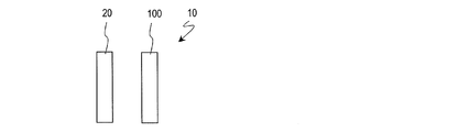
- It is a schematic diagram of a liquid crystal display device provided with the backlight unit shown in FIG.
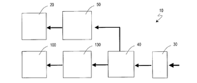
- FIG. 4 is a block diagram of the liquid crystal display device shown in FIG. 3.
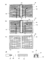
- (A) And (b) is a typical rear view of the backlight unit shown in FIG. 1
- (c) is a schematic front view of the backlight unit shown in FIG. 1
- (d) is It is a typical rear view of the LED substrate in the backlight unit shown in FIG.
- (e) is a schematic front view of the LED substrate shown in (d)
- (f) is shown in (d). It is the typical partial sectional view of the LED board.
- (A) is a typical front view of the backlight unit of Comparative Example 1
- (b) is a schematic exploded side view of (a).
- (A) It is a graph which shows the time change of the temperature of each location of the backlight unit of the comparative example 1
- (b) is a graph which shows the time change of the temperature of each location of the backlight unit of 1st Embodiment. It is a graph which shows the equilibrium temperature of the backlight unit of 1st Embodiment and Comparative Example 1.
- (A) is a typical front view of the backlight unit of Comparative Example 2, and (b) is a schematic exploded side view of (a).
- (A) is a typical front view which shows the model of the backlight unit shown in FIG. 1
- (b) is a typical top view of (a).
- (A), (b), and (c) are the graphs which respectively show the equilibrium temperature of the model of the backlight unit of the comparative example 1, the comparative example 2, and 1st Embodiment. It is a graph which shows the equilibrium temperature of the model of the backlight unit of the comparative example 1 and 1st Embodiment.
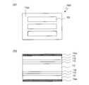
- (A) is a schematic diagram of 2nd Embodiment of the backlight unit by this invention
- (b) is typical sectional drawing of the chassis in (a).
- FIG. 1 is a schematic diagram of 3rd Embodiment of the backlight unit by this invention
- FIG. 2 is a schematic cross-sectional view of the chassis in FIG.
- A) is a schematic diagram of 4th Embodiment of the backlight unit by this invention
- (b) is a typical disassembled perspective view of the chassis in (a).
- (A)-(c) is a schematic diagram for demonstrating the manufacturing method of the chassis of the backlight unit shown in FIG.
- FIG. 1 is a schematic diagram for demonstrating the production method of another chassis of the backlight unit shown in FIG.
- FIG. 6 is a schematic rear view of still another embodiment of a backlight unit according to the present invention.
- (A) is a typical exploded side view of the backlight unit of the reference example
- (b) is a schematic rear view of the backlight unit shown in (a). It is a graph which shows the equilibrium temperature of the backlight unit of a reference example, and the backlight unit shown in FIG.
- FIG. 21 is a graph showing the equilibrium temperature of the backlight unit of the reference example and the backlight unit shown in FIGS.
- FIG. 1A shows a schematic front view of the backlight unit 100 of the present embodiment.
- the backlight unit 100 includes a chassis 110 and a light source 120 attached to the chassis 110.
- a light emitting diode (LED) is used as the light source 120.
- a cold cathode fluorescent lamp (CCFL) may be used.
- CCFL cold cathode fluorescent lamp
- FIG. 1B shows a schematic exploded perspective view of the chassis 110.
- the chassis 110 includes an aluminum substrate 112 and a porous alumina layer 114a that has been subjected to sealing treatment.
- the porous alumina layer 114 a is provided on the surface of the aluminum substrate 112.
- the thickness of the aluminum substrate 112 is preferably 1.0 mm or more, for example, 1.5 mm.
- the thickness of the porous alumina layer 114a is, for example, about 10 ⁇ m.
- An aluminum base 112 having a relatively high thermal conductivity exists inside the chassis 110, and a porous alumina layer 114a made of aluminum oxide having a relatively high thermal emissivity is provided on the surface of the aluminum base 112. It has been.
- the chassis 110 When the light source 120 is turned on, heat is generated by the current supplied to the light source 120. When such heat is transferred to the chassis 110, the heat is efficiently transferred to the entire aluminum base 112 having a high thermal conductivity, and is efficiently radiated to the outside by the porous alumina layer 114a having a high thermal emissivity. Is done. For this reason, the chassis 110 can efficiently release the heat generated in the backlight unit 100 to the outside, and can ensure the operational stability.
- the chassis 110 is formed as follows. First, an aluminum substrate 112 having a thickness of 1.5 mm is prepared.
- the aluminum substrate 112 is relatively high in rigidity.
- the aluminum purity in the aluminum substrate 112 is 99.50 mass% or more and less than 99.99 mass%.
- the aluminum substrate 112 contains impurities. This impurity is at least one element selected from the group consisting of Fe, Si, Cu, Mn, Zn, Ni, Ti, Pb, Sn, and Mg, and the aluminum substrate 112 preferably contains Mg as an impurity. .
- Such an aluminum substrate is also called an aluminum alloy.
- Anodic oxidation uses, for example, a sulfuric acid aqueous solution having a concentration of 10% by mass to 20% by mass and a bath temperature of 20 ° C. to 30 ° C. as an electrolyte, and a current density DC of 1 A / dm 2 to 2 A / dm 2 , applied voltage It is carried out by immersing the aluminum substrate 112 at 10 V or more and 30 V or less for 10 minutes or more and 30 minutes or less, whereby a porous alumina layer is formed. Note that.
- Such anodization is also called alumite treatment, and a film formed by the alumite treatment is also called an alumite film.
- the etching process is performed using, for example, 10% by mass of phosphoric acid, an aqueous solution of an organic acid such as formic acid, acetic acid, or citric acid or a mixed aqueous solution of chromium phosphoric acid as an etching solution.
- the sealing treatment is performed using pressurized steam and boiling water.
- the sealing treatment may be performed by applying water vapor of several atmospheres.
- the sealing treatment may be performed by heating for several tens of minutes with boiling water adjusted to about pH 5.5 to 6.5.
- a sealing agent such as nickel acetate may be added.
- the chassis 110 is formed as described above.
- FIG. 2 shows a schematic disassembled side surface portion of the backlight unit 100.
- the chassis 110 has a front surface 110 a and a back surface 110 b, and the light source 120 is provided on the front surface 110 a of the chassis 110.
- the backlight unit 100 is further provided with a light source driving unit 130 that controls the light source 120.
- the light source 120 is provided on the front surface 110 a of the chassis 110, whereas the light source driving unit 130 is provided on the back surface 110 b of the chassis 110.
- an opening 116 (see FIG. 5B) is provided in the chassis 110, and electrical connection between the light source 120 and the light source driving unit 130 is performed through the opening 116.
- the light source driving unit 130 includes a light source control circuit 132 and a light source control board 134 that supports the light source control circuit 132.
- the light source control circuit 132 is mounted as an integrated chip.
- the guaranteed operating temperature of the light source control circuit 132 is about 120 ° C.
- the light source control board 134 includes an insulating board and wiring provided on the insulating board.
- the insulative substrate is, for example, Flame Regentant Type 4 (FR4).
- the light source driving unit 130 drives the light source 120
- heat is generated from the light source driving unit 130.
- the amount of heat generated in the light source driving unit 130 is higher than the amount of heat generated in the light source 120
- the temperature of the light source driving unit 130 is higher than that of the light source 120.
- heat generated from the light source driver 130 is transmitted to the chassis 110 when the light source driver 130 is driven, the heat is efficiently transmitted to the entire aluminum substrate 112 by the aluminum substrate 112 having high thermal conductivity. And is efficiently radiated to the outside by the porous alumina layer 114a having a high thermal emissivity. For this reason, the chassis 110 can efficiently release the heat generated from the light source driving unit 130 to the outside, and can ensure operational stability.
- the chassis 110 to which the light source 120 is attached is covered with, for example, a cover member (not shown here).
- FIG. 3 shows a schematic diagram of the liquid crystal display device 10 including the backlight unit 100.
- the liquid crystal display device 10 includes a backlight unit 100 and a liquid crystal panel 20.
- the liquid crystal panel 20 has a plurality of pixels arranged in a matrix of a plurality of rows and a plurality of columns.
- a red pixel, a green pixel, and a blue pixel are provided as pixels
- a color display pixel composed of a red pixel, a green pixel, and a blue pixel functions as a display unit of an arbitrary color.
- the color display pixel may further include another pixel (for example, a yellow pixel) in addition to the red, green, and blue pixels.
- the color display pixel may further include a white pixel in addition to the red, green, and blue pixels, thereby increasing the luminance efficiently.
- the liquid crystal panel 20 includes a front substrate, a rear substrate, and a liquid crystal layer sandwiched between them.
- the backlight unit 100 may be a direct type.
- a diffusion plate, a lens sheet (H2K), a brightness enhancement film (Brightness Enhancement Film: BEF), another brightness enhancement film (Dual Brightness Enhancement Film: DBEF) are sequentially arranged between the chassis 110 and the liquid crystal panel 20. It may be provided.
- the backlight unit 100 may be an edge type.
- a light guide plate may be installed in the cover member together with the chassis 110 to which the light source 120 is attached.
- FIG. 4 shows a block diagram of the liquid crystal display device 10.
- the liquid crystal display device 10 includes a liquid crystal panel 20, a signal input unit 30, a video processing unit 40, a signal conversion unit 50, a light source driving unit 130, and a backlight unit 100.
- An input video signal is input to the signal input unit 30.
- the video processing unit 40 generates a display signal and a backlight drive signal based on the input video signal.
- the signal converter 50 generates a scanning signal, a source signal, and the like based on the display signal.
- the light source driving unit 130 controls the light source 120 (see FIG. 2) based on the backlight driving signal.
- the light source driving unit 130 is provided in the timing controller. As will be described later, the light source driving unit 130 may be attached to the backlight unit 100.
- any of the signal input unit 30, the video processing unit 40, and the signal conversion unit 50 may be mounted on the frame area of the liquid crystal panel 20.
- the light source driving unit 130 may control the lighting of the light source 120 for each region as necessary, thereby performing display with a high contrast ratio.
- an LED is preferably used as the light source 120.
- a light source driving unit, a light source control circuit, and a light source control board when an LED is used as the light source 120 may be referred to as an LED driving unit, an LED control circuit, and an LED control board, respectively.
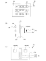
- FIG. 5A shows the back surface of the backlight unit 100.
- the LED driving unit 130 is disposed at the center of the back surface 110b of the chassis 110, and the flexible substrate 136 extends from the LED driving unit 130 in the left direction or the right direction.
- the flexible substrate 136 is disposed on the back surface 110b of the chassis 110, but the present invention is not limited to this.
- the flexible substrate 136 is provided on the front surface 110a of the chassis 110, the LED 120 cannot be installed in a portion covered with the flexible substrate 136, and luminance unevenness may occur. Further, if the flexible substrate 136 is provided on the side surface of the chassis 110, the frame area is enlarged.
- the flexible substrate 136 on the back surface 110b of the chassis 110, whereby the luminance unevenness of the LED 120 and the expansion of the frame area can be suppressed.
- the flexible boards 136 are arranged in a plurality of rows in the left column and the right column on the back surface 110b of the chassis 110, and here, 24 flexible boards 136 are arranged in 12 rows and 2 columns. Is arranged.
- FIG. 5B is a diagram in which one upper right flexible board 136 is removed from the backlight unit 100 shown in FIG. As shown in FIG. 5B, the chassis 110 is provided with openings 116 corresponding to the respective flexible boards 136.
- FIG. 5C shows the front surface of the backlight unit 100.
- a plurality of LED substrates 122 each extending in the lateral direction are attached to the front surface 110 a of the chassis 110, and each LED substrate 122 is provided with a plurality of LEDs 120.
- the LED 120 is attached to the chassis 110 via the LED substrate 122.
- the LED substrate 122 on the front surface 110a of the chassis 110 is provided corresponding to the flexible substrate 136 on the back surface 110b of the chassis 110.
- the LED boards 122 are arranged on a front surface 110a of the chassis 110 over a plurality of rows in each of two columns of the left column and the right column, and 24 LED boards 122 are arranged in 12 rows and 2 columns. ing.
- FIG. 5D shows the back surface of the LED substrate 122.
- a connection portion 124 is attached to the back surface of the LED substrate 122.
- the size of the connection portion 124 is designed to match the size of the opening portion 116 of the chassis 110 shown in FIG.
- the connection portion 124 protrudes from the opening portion 116 of the chassis 110 to the back surface 110 b, and the connection portion 124 can be communicated with the flexible substrate 136.
- the light source 120 is electrically connected to the LED control circuit 132 via the connection portion 124 and the flexible substrate 136.
- FIG. 5E shows the front surface of the LED substrate 122.
- a plurality of LEDs 120 are provided on the front surface of the LED substrate 122.
- FIG. 5F shows a cross section of one LED 120 on the LED substrate 122.
- a wiring 126 is provided between the LED 120 and the LED substrate 122.
- the width of the wiring 126 can be increased without omitting a circuit provided on the LED substrate 122, and a large current can be supplied to the LED 120.
- wiring may also be formed on the back surface of the LED substrate 122.
- the LED 120 is electrically connected to the LED driving unit 130 via the flexible substrate 136.
- LED120 was attached to the front surface 110a of the chassis 110 via the LED board 122 here, this invention is not limited to this.
- the LED 120 may be attached to the front surface 110 a of the chassis 110 without being attached to the LED substrate 122.
- the backlight unit 100 When the liquid crystal display device 10 is used as a general television device, the backlight unit 100 needs to have a luminance of about 500 cd / m 2 , whereas the digital signage used outdoors is a liquid crystal display device. when using the 10, the back light unit 100 is 1000 cd / m 2 or more (more preferably about 2500 cd / m 2) should have a brightness of.
- the output luminance of the backlight unit 100 is about 450 cd / m 2 , and the total power of the light source 120 and the light source driving unit 130 is about 100 W. And a current of about 1.0 A flows.
- the output luminance of the backlight unit 100 is about 2000 cd / m 2 , and the total power of the light source 120 and the light source driving unit 130 is about It is 400 W, and a current of about 9.0 A flows.
- a large current flows in this way, further improvement in the heat dissipation characteristics of the backlight unit is required.
- FIG. 6A shows a schematic front view of the backlight unit 700 of Comparative Example 1
- FIG. 6B shows a schematic exploded side view of the backlight unit 700.
- the backlight unit 700 has the same configuration as the backlight unit 100 except that the chassis 710 is formed from an electrogalvanized steel sheet (Steel Electric Cold Commercial: SECC).
- SECC Step Electric Cold Commercial
- the LED 720 is provided on the front surface 710a of the chassis 710 via an insulating sheet 750 in order to prevent conduction between the chassis 710 and the LED 720.
- the temperature measurement was performed using thermocouples on the rear surfaces 110b and 710b of the chassis 110 and 710, the LEDs 120 and 720, and the LED control circuits 132 and 732.
- the measurement of the backlight unit 100 is performed by adjusting the parameters of the signals generated in the video processing unit 40 and / or the LED driving unit 130 shown in FIG. 4, and the measurement of the backlight unit 700 is performed in the same manner.
- the horizontal axis indicates the time since the start of lighting of the LEDs 120 and 720
- the vertical axis indicates the temperature of each part of the backlight units 100 and 700.
- FIG. 7A is a graph showing the temperature change of the backlight unit 700.
- A1 indicates the temperature change of the LED control circuit 732
- A2 indicates the temperature change of the LED 720
- A3 indicates the temperature change of the back surface 710b of the chassis 710. Note that the temperature in the air away from the backlight unit 700 is about 22 ° C.
- FIG. 7B is a graph showing the temperature change of the backlight unit 100.
- B1 indicates the temperature change of the LED control circuit 132
- B2 indicates the temperature change of the LED 120
- B3 indicates the temperature change of the back surface 110b of the chassis 110.
- the LED 120 is provided on the front surface 110a of the chassis 110 via an insulating sheet 150 (see FIG. 10).
- FIGS. 7 (a) and 7 (b) the temperature reaches an equilibrium state in about 40 minutes.
- FIG. 7 (a) and FIG. 7 (b) show the temperatures at which the equilibrium state is reached, and such temperatures are also referred to as equilibrium temperatures in this specification.
- the equilibrium temperature of each part in the backlight unit 100 is lower by about 7 to 10 ° C. than that of the backlight unit 700.
- the porous alumina layer 114a having a high thermal emissivity is provided on the surface, so that it is considered that the heat dissipation is improved.
- the aluminum base 112 having a higher thermal conductivity than SECC exists inside the chassis 110, the heat transmitted to the chassis 110 spreads throughout the chassis 110, and as a result, heat is dissipated throughout the chassis 110. This is considered to be done efficiently.
- the equilibrium temperature in the chassis 110 is compared, the equilibrium temperature of the LED control circuit 132 is the highest and the equilibrium temperature of the back surface 110b of the chassis 110 is the lowest.
- FIG. 8 shows the equilibrium temperature of the backlight units 100 and 700.
- the temperatures of the LEDs 120 and 720 and the LED driving units 130 and 730 are measured.
- the backlight unit 100 includes a plurality of LEDs 120, but the forward voltage Vf of the LEDs 120 is not constant and varies.
- the LED driving unit 130 supplies common power to the LEDs 120 so that the LEDs 120 having a high forward voltage Vf are turned on, excessive power is supplied to the LEDs 120 having a low forward voltage Vf. Will be.
- the LED drive part 130 may suppress that excess electric power is supplied to LED120 with the low forward voltage Vf. In this case, this electric power is generated as heat in the LED control circuit 132.
- the equilibrium temperature of the LEDs 120 and 720 and the LED driving units 130 and 730 increases by 20 ° C. or more by providing the cover member. This is considered because the air flow is obstructed by the cover member.
- the equilibrium temperature of the backlight units 100 and 700 individually.
- the equilibrium temperature of the LED 720 in the backlight unit 700 is higher than that of the LED driving unit 730. This is considered because the average value of the forward voltage Vf of the LED 720 is high, so that an excessive power supply is required and a lot of heat is generated in the LED 720.
- the equilibrium temperature of the LED driving unit 130 in the backlight unit 100 is higher than that of the LED 120. This is presumably because the heat generated in the LED 120 was efficiently released by the chassis 110.
- the equilibrium temperature of the LED 720 in the backlight unit 700 is lower than that of the LED driving unit 730. This is probably because heat from the LED driving unit 730 is hardly released by the cover member.
- the equilibrium temperature of the LED driving unit 130 in the backlight unit 100 is higher than that of the LED 120. This is considered because not only the heat generated in the LED 120 is efficiently released by the chassis 110 but also the heat from the LED driving unit 130 is hardly released by the cover member.
- the equilibrium temperature of the LED 120 and the LED 720 When the cover member is not provided, the equilibrium temperature of the LED 120 is 10 ° C. or lower than that of the LED 720. When the cover member is provided, the equilibrium temperature of the LED 120 is 10 ° C. or lower than that of the LED 720. As described above, the equilibrium temperature of the LED 120 is lower than that of the LED 720 according to the chassis 110 and 710. It is considered that the difference between the equilibrium temperatures of the LEDs 120 and 720 is caused by the difference between the chassis 110 and 710. Note that the amount of change in the equilibrium temperature of the LEDs 120 and 720 due to the provision of the cover member is substantially equal to each other. This is probably because the power consumption of the LEDs 120 and 720 is approximately the same.
- the equilibrium temperature of the LED driving unit 130 and the LED driving unit 730 attention is paid to the equilibrium temperature of the LED driving unit 130 and the LED driving unit 730.
- the equilibrium temperature of the LED driving unit 130 is substantially equal to that of the LED driving unit 730.
- the equilibrium temperature of the LED driving unit 130 is substantially equal to that of the LED driving unit 730. This is presumably because the LED driving units 130 and 730 drive the LEDs 120 and 720 according to the forward voltage Vf of the LEDs 120 and 720, and the amount of heat generated from the LED driving units 130 and 730 is substantially equal.
- the change in the equilibrium temperature of the LED driving units 130 and 730 depending on the presence or absence of the cover member is larger than the change in the equilibrium temperature of the LEDs 120 and 720.
- the LED driving units 130 and 730 are disposed closer to the cover member than the LEDs 120 and 720, and the LED driving units 130 and 730 have their own low thermal conductivity insulating substrate (for example, FR4) and the cover member. Therefore, it is considered that the temperature is more likely to rise than the LEDs 120 and 720.
- the thermal emissivity of SECC is extremely low, less than 0.1, whereas the average emissivity of the chassis 110 depends on the thickness of the porous alumina layer 114. It is as high as about 0.78.
- the thermal emissivity of aluminum oxide is 0.85.
- the thermal conductivity of SECC is 53 W / mk, whereas the thermal conductivity of the aluminum base 112 is 120 W / mK.
- the thermal conductivity of pure aluminum is even higher at 236 W / mK, pure aluminum does not have sufficient strength.
- an aluminum base material 112 having a relatively higher mechanical strength than SECC Although some aluminum does not have sufficient strength, it is preferable to use an aluminum base material 112 having a relatively higher mechanical strength than SECC.
- the tensile strength, yield strength and elongation of SECC are 350 N / mm 2 , 213 N / mm 2 and 21%, respectively.
- an aluminum substrate 112 for example, tensile strength, yield strength and elongation, respectively, 400N / mm 2, 310N / mm 2, 12% of the aluminum alloy is preferably used.
- a 5000 series aluminum alloy may be used as the aluminum base 112.
- tensile strength, yield strength and elongation, respectively may be used 240N / mm 2, 190N / mm 2, 12% of% of aluminum alloy.
- the insulating sheet 750 is provided between the chassis 710 and the LED 720 in order to suppress conduction between the chassis 710 and the LED 720. For this reason, from the viewpoint of heat dissipation, the heat generated by the LED 720 is difficult to transfer to the chassis 710. Further, even if an insulating heat radiating sheet having a relatively high heat radiating property is used as the insulating sheet 750, the heat exhaust effect is small. This is presumably because the adhesive layer portion that adheres the insulating heat-radiating sheet is formed of a resin having low thermal conductivity.
- the dielectric breakdown voltage is 540V
- the dielectric breakdown voltage is 360V.
- the insulation resistance between the chassis 110 and the LED substrate 122 is sufficient.
- the surface Vickers hardness Hv of the porous alumina layer 114a is about 200, which is higher than the surface Vickers hardness Hv (50) of a general aluminum base material. It is equivalent to the surface Vickers hardness Hv (150 to 200).
- the specific gravity of aluminum (Al: 2.7) is about 1/3 compared to SECC (Fe: 7.8), and the chassis 110 is relatively light. It is suitably used for the liquid crystal display device 10. Moreover, corrosion resistance is also improved by providing the porous alumina layer 114a.
- the chassis 110 since the chassis 110 has the porous alumina layer 114a, the insulation between the chassis 110 and the light source 120 can be improved, and an insulating sheet is not used. Good. Of course, an insulating sheet may be provided between the chassis 110 and the LED substrate 122 as necessary.
- the backlight unit 700 of the comparative example 1 is the same as that described with reference to FIG. 6, and description thereof is omitted here.
- FIG. 9A shows a schematic front view of the backlight unit 800 of Comparative Example 2
- FIG. 9B shows a schematic exploded side view of the backlight unit 800.
- the backlight unit 800 has the same configuration as the backlight unit 100 except that the backlight unit 800 includes a chassis 810 formed from an aluminum base material that has not been anodized. Also in the backlight unit 800, the LED 820 is provided on the front surface 810 a of the chassis 810 via an insulating sheet 850 in order to prevent conduction between the chassis 810 and the LED 820.
- the thickness of the natural oxide film on the surface of the aluminum base is about several nm to several tens of nm.
- a model including one LED substrate 122, 722, and 822 and a chassis 110, 710, and 810 having a size corresponding to the LED substrate is manufactured to produce the LEDs 120, 720, and 820
- the main surfaces of the chassis 110, 710, and 810 of this model are about 10 cm long and about 30 cm wide, respectively.
- FIG. 10A shows a schematic front view of a model of the backlight unit 100
- FIG. 10B shows a top view.
- the LED 120 is attached to the front surface 110 a of the chassis 110 via the insulating sheet 150.
- the outer frame of the model is covered with foamed polystyrene, and an H2K sheet is disposed on the surface thereof as a lens sheet.
- BEF may be used instead of the H2K sheet.
- the models of the backlight units 700 and 800 are produced in the same manner as the model of the backlight unit 100 except that the chassis 710 and 810 are different.
- the thermal emissivity of SECC is extremely low, less than 0.1.
- the thermal emissivity of pure aluminum is 0.03, and the average emissivity of general aluminum is as low as 0.14.
- the average emissivity of the chassis 110 is as high as about 0.78 although it depends on the thickness of the porous alumina layer 114.
- the thermal emissivity of aluminum oxide is 0.85.
- the thermal conductivity of SECC is 53 W / mk.
- the heat conductivity of pure aluminum is as high as 236 W / mK, it does not have sufficient strength.
- general alumina has a thermal conductivity of 29 W / mK.
- the thermal conductivity of the aluminum substrate 112 is 120 W / mK.
- the equilibrium temperature of the models of the backlight units 100, 700, and 800 will be described with reference to FIG. It should be noted that here, it is important to compare the equilibrium temperatures of the backlight units 100, 700, and 800 under the same conditions and the same location, and the absolute value of the equilibrium temperature is not important. Specifically, here, the equilibrium temperatures of the models of the backlight units 100, 700, and 800 having a small size and a small calorific value are compared, and the equilibrium of the models of the backlight units 100, 700, and 800 is compared. The difference in temperature is smaller than the difference in actual equilibrium temperature between the backlight units 100, 700, and 800.
- FIG. 11A shows the equilibrium temperature of the LED substrates 122, 722, and 822 of the backlight units 100, 700, and 800.
- FIG. 10 the measurement location is indicated by L.
- the equilibrium temperature of the backlight unit 700 is the highest. This is considered because the chassis 710 is formed of SECC having a relatively low thermal emissivity, and the heat generated in the LED substrate 722 is not easily released through the insulating sheet 750 and the chassis 710. Further, the equilibrium temperature of the backlight unit 100 is the lowest. This is presumably because the surface of the chassis 110 is formed of a porous alumina layer 114 a having a relatively high thermal emissivity, and the heat generated in the LED substrate 122 is easily released via the insulating sheet 150 and the chassis 110. Thus, it is considered that the equilibrium temperature differs mainly depending on the magnitude of the thermal emissivity of the chassis 110, 710, 810.
- FIG. 11B is a graph showing the temperatures of the regions overlapping the LED substrates 122, 722, and 822 in the back surfaces 110b, 710b, and 810b of the chassis 110, 710, and 810. In FIG. 10, this measurement point is indicated by M.
- the equilibrium temperature of the backlight unit 700 is the highest, and the equilibrium temperature of the backlight unit 100 is the lowest.
- the equilibrium temperature is considered to vary mainly depending on the magnitude of the thermal emissivity of the chassis 110, 710, and 810.
- FIG. 11C is a graph showing the temperatures of the regions that do not overlap with the LED boards 122, 722, and 822 of the back surfaces 110b, 710b, and 810b of the chassis 110, 710, and 810b.
- this measurement location is indicated as N. This location N is 5 cm away from the corresponding ends of the LED substrates 122, 722, and 822.
- the equilibrium temperature of the backlight unit 800 is the highest.
- the chassis 810 is formed of aluminum having a relatively high thermal conductivity and a relatively low thermal emissivity, and the heat generated in the LED substrate 822 moves through the insulating sheet 850 and the chassis 810 while the chassis 810. It is thought that it is difficult to be released from the water. Further, the equilibrium temperature of the backlight unit 100 is the lowest. This is because the chassis 110 not only has the aluminum base 112 inside but also has a porous alumina layer 114a on the surface, and heat generated in the LED substrate 122 moves through the insulating sheet 150 and the chassis 110, This is considered to be easily released from the chassis 110.
- the temperature can be lowered as compared with the backlight units 700 and 800 of Comparative Examples 1 and 2, and thus the operation stability can be further ensured. it can.
- the insulating sheet 150 is also provided in the backlight unit 100, but a porous alumina layer 114 a is provided on the surface of the chassis 110.
- the insulating sheet 150 does not need to be provided in the backlight unit 100 because it exhibits high insulation.
- the temperature of the backlight unit 100 can be further reduced.
- the temperature of the LED substrate 122 is 42.2 ° C.
- the equilibrium temperature of the LED substrate 122 can be further lowered as compared with the backlight unit 700.
- the cost of the insulating sheet 150 can be suppressed by not using the insulating sheet 150 in this way.
- a fan may be provided on the back surface 110 b of the chassis 110 in the backlight unit 100.
- the anodization is performed on the aluminum base material, but the present invention is not limited to this. Even if an aluminum substrate is not used, the same effect can be obtained by forming an aluminum layer by vapor deposition or the like and then anodizing the aluminum layer. In this case, in order to improve the adhesion between the substrate and the aluminum layer, it is preferable to deposit the inorganic underlayer and the buffer layer together.
- the buffer layer contains aluminum and oxygen or nitrogen, and it is preferable to change the aluminum content in the buffer layer so that the aluminum content on the aluminum layer side in the buffer layer is higher than that of the inorganic underlayer.
- the backlight unit 100A of the present embodiment has the same configuration as that of the backlight unit described above with reference to the first embodiment except that the configuration of the chassis is different, and redundant description is given to avoid redundancy. Omitted.
- FIG. 13A shows a schematic diagram of the backlight unit 100A of the present embodiment
- FIG. 13B shows a schematic sectional view of the chassis 110A in the backlight unit 100A
- the chassis 110A further includes an inorganic underlayer 115, a buffer layer 116, and an aluminum layer 117 between the base material 112 and the porous alumina layer 114a.
- a glass substrate or a plastic film is used as the substrate 112.
- a polyethylene terephthalate (Polyethylene terephthalate: PET) film or a triacetyl cellulose (TAC) film is used as the plastic film.
- SECC may be used as the substrate 112.
- the inorganic base layer 115 is formed on the surface of the substrate 112, the buffer layer 116 is formed on the inorganic base layer 115, and the aluminum layer 117 is formed on the surface of the buffer layer 116.
- the porous alumina layer 114a is formed by subjecting the aluminum layer 117 to anodic oxidation (etching treatment if necessary) and sealing treatment. Note that in the case where a conductive layer is provided as a base in order to uniformly anodize the aluminum layer 117, the conductive layer is provided between the inorganic base layer 115 and the buffer layer 116 or between the buffer layer 116 and the aluminum layer 117. It is preferable to provide (preferably a valve metal layer).
- the inorganic base layer 115 is directly formed on the surface of the substrate 112 and acts to prevent the alkali metal element contained in the substrate 112 from eluting.
- the substrate 112 it is preferably formed of an inorganic oxide or an inorganic nitride.
- an inorganic oxide for example, a silicon oxide layer or a titanium oxide layer is preferable.
- an inorganic nitride for example, a silicon nitride layer is preferable.
- the thermal expansion coefficient can be increased by adding germanium (Ge), phosphorus (P), or boron (B).
- Ge germanium
- P phosphorus
- B boron
- the thermal expansion coefficient becomes about 2.8 ⁇ 10 ⁇ 6 / ° C., which is about three times that when Ge is not added.
- the thickness of the inorganic base layer 115 is preferably 40 nm or more, and more preferably 100 nm or more. In addition, the thickness of the inorganic base layer 115 is preferably 500 nm or less, and more preferably 200 nm or less. If the thickness of the inorganic underlayer 115 exceeds 500 nm, the formation time of the inorganic underlayer 115 becomes unnecessarily long. In addition, the adhesive force between the base material 112 and the inorganic base layer 115 may be reduced due to thermal stress (shear stress) caused by the difference in thermal expansion coefficient between the base material 112 and the inorganic base layer 115. . Further, when a flexible base material such as a plastic film is used as the base material 112, when the thickness of the inorganic base layer 115 exceeds 500 nm, the inorganic base layer is bent when the base material is bent. 115 may be cracked.
- the buffer layer 116 is provided between the inorganic base layer 115 and the aluminum layer 117 and acts to improve the adhesion between the inorganic base layer 115 and the aluminum layer 117.
- the buffer layer 116 is made of a material having excellent acid resistance, and protects the inorganic base layer 115 from acid.
- the buffer layer 116 preferably contains aluminum and oxygen or nitrogen. Although the content of oxygen or nitrogen may be constant, it is particularly preferable that the aluminum content has a higher profile on the aluminum layer 117 side than on the inorganic underlayer 115 side. It is because it is excellent in matching of physical property values such as thermal expansion coefficient.
- the thickness of the buffer layer 116 is preferably 40 nm or more, more preferably 100 nm or more, and the thickness of the buffer layer 116 is preferably 500 nm or less, and more preferably 200 nm or less. preferable.
- the inorganic underlayer 115 is sufficiently protected from the treatment liquid that permeates from the aluminum layer 117 side (the electrolytic solution in the anodizing step and / or the etching solution in the etching step).
- the effect of providing the buffer layer 116 may not be sufficiently exhibited.
- the thickness of the buffer layer 116 is more than 500 nm, it is not preferable because the formation time of the buffer layer 116 becomes unnecessarily long.
- the profile in the thickness direction of the aluminum content in the buffer layer 116 may change stepwise or may change continuously.
- the buffer layer 116 is formed of aluminum and oxygen
- a plurality of aluminum oxide layers whose oxygen content gradually decreases are formed, and the aluminum layer 117 is formed on the uppermost layer.
- the buffer layer 116 containing aluminum and nitrogen is formed.
- the aluminum layer 117 is formed by a known method (for example, an electron beam evaporation method or a sputtering method).
- the aluminum layer 117 is formed by a sputtering method using an aluminum target having a purity of, for example, 99.99% by mass or more.
- the thickness of the aluminum layer 117 is, for example, 1000 nm (1 ⁇ m).
- it is preferable that the aluminum layer 117 having a thickness of about 1 ⁇ m is deposited in a plurality of times rather than in a single deposition. That is, rather than continuously depositing to a desired thickness (for example, 1 ⁇ m), the process of interrupting the deposition to a certain thickness and restarting the deposition after a certain time has elapsed is repeated.
- the aluminum layer 117 It is preferable to obtain the aluminum layer 117. For example, it is preferable to interrupt each time an aluminum layer having a thickness of 50 nm is deposited and to obtain an aluminum layer 117 having a thickness of about 1 ⁇ m by 20 aluminum layers each having a thickness of 50 nm.
- the quality for example, chemical resistance and adhesiveness
- the continuous deposition of aluminum increases the temperature of the substrate (referring to the one having the surface on which the aluminum layer is deposited), resulting in a distribution of thermal stress in the aluminum layer 117, reducing film quality. It is thought to make it.
- the aluminum layer 117 and the porous alumina layer 114a are provided on both the front surface 110a and the back surface 110b of the chassis 110A, but the present invention is not limited to this.
- the aluminum layer 117 and the porous alumina layer 114a may be provided only on one of the front surface 110a and the back surface 110b of the chassis 110A.
- the backlight unit 100B of the present embodiment has the same configuration as the backlight unit described above with reference to Embodiments 1 and 2 except that the thickness of the porous alumina layer in the chassis 110 is not constant. In order to avoid redundancy, redundant description is omitted.
- FIG. 14A shows a schematic diagram of the backlight unit 100B of the present embodiment
- FIG. 14B shows a schematic exploded perspective view of the chassis 110.
- the chassis 110 includes the aluminum base 112 and the porous alumina layer 114a having different thicknesses.
- the porous alumina layer 114a1 by immersing the entire aluminum base material 112 in the electrolytic solution and performing anodization, only a part of the aluminum base material 112 is immersed in the electrolytic solution, and the rest is immersed in the electrolytic solution.
- a porous alumina layer 114a2 is formed by performing anodization without performing a sealing process.
- porous alumina layers 114a having different thicknesses may be formed. Since the volume of the porous alumina layer increases due to expansion due to anodization, the thickness of the porous alumina layer 114a2 having a long total immersion time is thicker than that of the porous alumina layer 114a1 having a short total immersion time.
- the porous alumina layers 114a having different thicknesses are provided on the surface of the aluminum base 112, but the present invention is not limited to this. While the porous alumina layer is provided in a partial region of the aluminum substrate, the porous alumina layer may not be provided in the other region.
- FIG. 14C shows a schematic exploded perspective view of another chassis 110.
- the porous alumina layer 114a is provided only on one side (here, the left side as viewed in the drawing) of the aluminum substrate 112, and the porous alumina layer is provided on the other side.
- Such a porous alumina layer 114a is formed by immersing only a part of the aluminum substrate 112 in the electrolytic solution and performing anodic oxidation without immersing the rest in the electrolytic solution.
- FIGS. 14B and 14C partial anodization is performed on the aluminum base 112, but the present invention is not limited to this.
- the anodic oxidation may be partially performed by immersing the aluminum base material 112 or the aluminum layer 117 in an electrolytic solution in a masking state in which a part of the surface of the aluminum base material 112 or the aluminum layer 117 is covered with a protective film.
- a protective film a film with high acid resistance is used, for example.
- FIG. 14D shows a schematic cross-sectional view of the chassis 110A.
- the chassis 110 ⁇ / b> A includes the base material 112, the porous alumina layer 114 a, the inorganic base layer 115, the buffer layer 116, and the aluminum layer 117.
- the porous alumina layer 114a can be partially formed.
- a porous alumina layer 114a is partially provided on the surface of the aluminum layer 117.
- the entire surface of the aluminum layer 117 has a different thickness.
- a porous alumina layer 114a may be provided.
- the thermal radiation can be improved by increasing the thickness of the porous alumina layer 114a in a region where heat dissipation is particularly required. Further, by partially providing the porous alumina layer 114a, the surface area of the porous alumina layer 114a can be increased, and the heat dissipation characteristics can be improved.
- the backlight unit 100C of this embodiment has the same configuration as the backlight units of the above-described embodiments 1 to 3 except that the porous alumina layer is not sealed, and avoids redundancy. Therefore, the overlapping description is omitted.
- FIG. 15A shows a schematic diagram of the backlight unit 100C
- FIG. 15B shows an exploded perspective view of the chassis 110.
- the chassis 110 has an aluminum base 112 and a porous alumina layer 114b.
- the porous alumina layer 114b is formed by anodizing the aluminum substrate 112, and the sealing treatment is not performed.
- pores are formed after the anodic oxidation.
- the heat radiation effect can be increased by utilizing a relatively large surface area of the porous alumina layer 114b. .
- the surface area is increased as compared with the porous alumina layer formed by general anodization, and the area in contact with the outside air is increased.
- the heat dissipation effect by convection can be increased.
- a porous alumina layer 114b used as a so-called antireflection material mold (stamper) is formed as the porous alumina layer 114b. It is preferable to form a plurality of recesses having a length of 10 nm to less than 500 nm. Strictly speaking, the oxidation proceeds slightly by air without performing the sealing treatment.
- recesses having different sizes can be formed by performing anodization and etching on an aluminum base material containing at least one element selected from the group consisting of Mn, Mg, and Fe.
- recesses having different sizes can be formed by performing cathodic electrolysis before anodic oxidation.
- Such a porous alumina layer 114b is formed as follows, for example.
- the aluminum base material 112 whose aluminum (Al) content rate is 99.0 mass% or less is prepared.
- the aluminum substrate 112 preferably contains at least one element selected from the group consisting of Mn, Mg and Fe, and the total content of these elements is preferably 1% by mass or more.
- the aluminum substrate 112 may further contain Si.
- a porous alumina layer is formed by anodizing the surface portion of the aluminum substrate 112.
- a plurality of recesses are formed in the porous alumina layer.
- a plurality of fine recesses of the porous alumina layer are enlarged to form recesses (pores) 114p.
- the recess 114p is formed when the aluminum base 112 is 99.0% by mass or less, particularly when it contains at least one element selected from the group consisting of Mn, Mg and Fe.
- the number of the concave portions 114p decreases, and when it exceeds 99.5% by mass, the number decreases.
- the recesses 114p are formed when the porous alumina layer is first etched, and the number and size of the recesses 114p hardly change in the subsequent multiple etchings.
- the concave portions 114p are irregularly distributed.
- the anodic oxidation step and the etching step are alternately performed a plurality of times, thereby forming a plurality of fine concave portions 114q each having a stepped side surface in the porous alumina layer.
- the fine recess 114q is formed on the entire surface of the aluminum base 112 including the inner surface of the recess 114p.
- the porous alumina layer 114b is formed in this way.
- the size, generation density, depth, and the like of the recess 114q can be controlled by the conditions of anodization (for example, the formation voltage, the type and concentration of the electrolytic solution, and the anodization time). Further, the regularity of the arrangement of the recesses 114q can be controlled by controlling the magnitude of the formation voltage.
- the conditions for obtaining a highly ordered array are (1) anodizing at an appropriate constant voltage unique to the electrolyte and (2) anodizing for a long time. It is known that the combination of the electrolytic solution and the formation voltage at this time is 28 V for sulfuric acid, 40 V for oxalic acid, and 195 V for phosphoric acid.
- the process (1) is the same, but the time required for anodization is shortened as much as possible, and the etching process and the anodization process are alternately repeated.
- the formation of such a porous alumina layer 114b is disclosed in, for example, International Publication No. 2009/147858. In this specification, the content disclosed in International Publication No. 2009/147858 is incorporated by reference.
- porous alumina layer 114b in which concave portions (pores) having different sizes are formed can be formed by another method.
- a method of forming the porous alumina layer 114b will be described with reference to FIG.
- an aluminum substrate 112 is prepared.
- the aluminum substrate 112 may have a deteriorated layer.
- an aluminum layer 117 (see FIG. 13B) supported by a substrate such as a glass substrate (for example, a thickness of about 0.5 ⁇ m to 5 ⁇ m) can be used.
- the surface of the aluminum base material 112 or the aluminum layer 117 is used as a cathode, and a current is applied between the surface and the counter electrode, whereby the surface normal line is obtained.
- a plurality of concave portions (first concave portions) 114p having a two-dimensional size of 200 nm to 100 ⁇ m when viewed from the direction is formed.
- the aqueous solution electrolytic solution
- an electrolytic solution used for anodic oxidation can be used, or water having a resistance value of 1 M or less can be used.
- the liquid temperature By adjusting the time of cathodic electrolysis within a current range of, for example, about 1 to 100 A / dm 3 , the recess 114p having a two-dimensional size of 200 nm to 100 ⁇ m can be formed.
- a fine concavo-convex structure with a two-dimensional size of about several tens of nm can be formed as described above, and the two-dimensional size is 200 nm or more.
- a recess 114p of 100 ⁇ m or less can also be formed.
- the adjacent average distance of the recess 114p can vary depending on the conditions of cathodic electrolysis, but the adjacent average distance of the recess 114p is preferably 0.5 ⁇ m or more and 100 ⁇ m or less.
- FIG. 17 (c) by anodizing the surface, it is two-dimensional when viewed from the normal direction of the surface between the inner surfaces of the plurality of recesses 114p and the plurality of recesses 114p.
- a porous alumina layer having a plurality of fine recesses (second recesses) 114q having a size of 10 nm or more and less than 500 nm is formed. Further thereafter, the porous alumina layer is brought into contact with the etching solution to enlarge the plurality of minute recesses 114q.
- a porous alumina layer having a fine recess 114q having a desired cross-sectional shape can be formed by alternately repeating the anodizing step and the etching step a plurality of times.
- the fine recess 114q enlarges the hole diameter by etching (the cross-sectional shape is substantially cone-shaped), and the two-dimensional size (diameter) of the fine recess 114q is substantially equal to the adjacent distance and is 10 nm or more and less than 500 nm. It is preferable to adjust so that.
- the fine recess 114q is formed so as to overlap with the recess 114p having a two-dimensional size of 200 nm or more and 100 ⁇ m or less.
- the porous alumina layer 114b is formed.
- the formation of such a porous alumina layer is disclosed in, for example, Japanese Patent Application No. 2009-255534.
- the disclosure of Japanese Patent Application No. 2009-255534 is incorporated by reference.
- a porous alumina layer 114b that does not perform sealing is formed instead of the porous alumina layer 114a in the backlight units 100 and 100 of the first to third embodiments. May be.
- FIG. 18 (a) is a schematic front view of the backlight unit 200
- FIG. 18 (b) is a schematic exploded side view of the backlight unit 200
- FIG. 18 (c) is a schematic view of the backlight unit 200. It is a typical back view.
- the backlight unit 200 includes a chassis 210 having a front surface 210a and a back surface 210b, an LED 220 provided on the front surface 210a, and a fan 240 provided on the back surface 210b.
- the LED 220 is provided on the front surface 210 a of the chassis 210 via the LED substrate 222.
- an LED driving unit 230 is provided on the back surface 210 b of the chassis 210.
- the LED drive unit 230 includes an LED control circuit 232 and an LED control board 234, and the LED control circuit 232 is attached to the back surface 210 b of the chassis 210 via the LED control board 234.
- the chassis 210 in the backlight unit 200 is covered with a cover member.
- two exhaust heat fans 240 a are provided as the fans 240.
- the heat exhaust fan 240a is disposed so as to be substantially perpendicular to the normal direction of the back surface 210b of the chassis 210, and thereby the heat of the backlight unit 200 is discharged.
- two exhaust heat fans 240a are provided, but the number of exhaust heat fans 240a may be one, or the number of exhaust heat fans 240a may be three or more.
- the operation of the LED and the LED driving unit may become unstable due to the generated heat.
- the liquid crystal display device is used as a display for digital signage (especially a large digital signage for outdoor use) Since a large current flows through the LED and the LED driver, the operation tends to become unstable.
- the heat generated from the LED 220 is efficiently discharged to the outside by the exhaust heat fan 240a, and thus the operation can be stabilized.
- FIG. 19A is a schematic front view of the backlight unit 200 ′
- FIG. 19B is a schematic exploded side view of the backlight unit 200 ′.
- the backlight unit 200 ′ has the same configuration as the backlight unit 200 described above except that the fan 240 is provided with not the exhaust heat fan 240a but the blower fan 240b, so as to avoid redundancy. A duplicate description is omitted.
- a blower fan 240 b is provided as the fan 240.
- the blower fan 240b is disposed so as to be substantially parallel to the normal direction of the back surface 210b of the chassis 210, whereby heat released from the back surface of the backlight unit 200 ′ is transmitted from the vicinity of the backlight unit 200 ′. You can keep away.
- the heat generated from the LED 220 and the LED driving unit 230 is efficiently transmitted far away by the blower fan 240 b, so that the operation can be stabilized.
- the backlight unit may include both a heat exhaust fan and a blower fan.
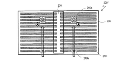
- FIG. 20 shows a schematic rear view of a backlight unit 200 ′′ according to another embodiment.
- the LED driving unit 230 is disposed at the center of the rear surface of the chassis 210, and the flexible substrate 236 extends from the LED driving unit 230 in the left direction or the right direction.
- both the exhaust heat fan 240 a and the blower fan 240 b are provided on the back surface 210 b of the chassis 210.
- two exhaust heat fans 240a are provided.
- the heat exhaust fan 240a is disposed so as to be substantially perpendicular to the normal direction of the rear surface 210b of the chassis 210, and thereby heat in the backlight unit 200 '' is discharged.
- the blower fan 240b is arranged so as to be substantially parallel to the normal direction of the back surface 210b of the chassis 210, whereby heat released from the back surface of the backlight unit 200 '' (most of which is exhausted heat).
- the heat discharged by the fan 240a is kept away from the vicinity of the backlight unit 200 ′′.
- the heat generated from the LED 220 and the LED drive unit 230 can be efficiently discharged. For this reason, stability of operation
- movement of LED220 and the LED drive part 230 is securable.
- the chassis 210 may be made of SECC, or the chassis 210 may be made of another material.
- the chassis 210 may have the above-described porous alumina layer on the surface thereof.
- the chassis 210 may have a porous alumina layer formed by anodizing (etching if necessary) an aluminum base material or an aluminum layer. Further, a porous alumina layer may be formed on the surface of the aluminum substrate or the aluminum layer by performing a sealing treatment.
- FIG. 21A shows a schematic diagram of a backlight unit 900 of a reference example
- FIG. 21B shows a schematic rear view of the backlight unit 900.
- the backlight unit 900 has the same configuration as the backlight unit 200 shown in FIG. 18 except that a fan is not provided.
- the backlight unit 900 includes a chassis 910 having a front surface 910a and a back surface 910b, an LED 920 attached to the front surface 910a of the chassis 910 via an LED substrate 922, and an LED driving unit 930 attached to the back surface 910b of the chassis 910. I have.
- chassis 210 and 910 having a porous alumina layer formed on the surface thereof by anodizing and sealing the aluminum base material are indicated as chassis 210p and 910p, respectively.
- the chassis 210 and 910 formed from SECC are indicated as chassis 210s and 910s, respectively.
- backlight units 200 and 900 having 210p, 210s, 910p, and 910s as the chassis 210 and 910 are denoted as backlight units 200a, 200b, 900a, and 900b, respectively.
- FIG. 22 shows the equilibrium temperatures of the backlight units 200a, 200b, 900a, and 900b.
- the temperatures of the LEDs 220 and 920 and the LED driving units 230 and 930 of the backlight units 200a, 200b, 900a, and 900b are measured.
- the backlight members 200a, 200b, 900a, and 900b are similarly provided with cover members, but for reference, the backlight units 900a and 900b that are not provided with cover members are provided.
- the temperature of is also measured.
- the equilibrium temperature of the LED 920 increases by about 25 ° C. by providing the cover member. Note that the amount of change in the equilibrium temperature of the backlight unit 900a is lower than that of the backlight unit 900b. This is probably because a porous alumina layer is provided on the surface of the chassis 910p, whereas the chassis 910s is made of SECC, and the thermal emissivity of the chassis 910p is higher than that of the chassis 910s.
- the equilibrium temperature can be reduced as compared with the backlight unit 900 of the reference example.
- the exhaust heat fan 240a can reduce the equilibrium temperature of the LEDs 220 in the backlight units 200a and 200b by about 20 ° C. as compared with the LEDs 920 of the backlight units 900a and 900b.
- the exhaust heat fan 240a can reduce the equilibrium temperature of the LED driving unit 230 in the backlight units 200a and 200b by about 30 ° C. compared to the LED driving unit 930 of the backlight units 900a and 900b.
- the temperature reduction effect of the LED drive unit 230 by the exhaust heat fan 240a is higher than that of the LED 220.
- the LED driving unit 230 is provided on the rear surface 210b of the chassis 210, whereas the LED 220 is provided on the front surface 210a of the chassis 210, and the heat exhaust fan 240a is heated near the rear surface 210b of the chassis 210. It is considered that the transmitted air is efficiently moved away from the rear surface 210b of the chassis 210.
- the reduction amounts of the equilibrium temperatures of the backlight units 200a and 200b by the exhaust heat fan 240a are substantially the same. Note that the equilibrium temperature of the backlight unit 200a is lower than that of the backlight unit 200b due to the difference between the chassis 210p formed of an aluminum base material having a porous alumina layer formed on the surface and the chassis 210s formed of SECC.
- the temperature of the backlight units 200a and 200b can be lowered by providing the exhaust heat fan 240a. Therefore, the operation of the LED 220 and the LED driving unit 230 can be stabilized.
- FIG. 23 shows a backlight unit 900, a backlight unit 900 without a cover member, a backlight unit 200 having a heat exhaust fan 240a, a backlight unit 200 ′ having a blower fan 240b, and a heat exhaust fan 240a and a blower.
- the measurement results of the equilibrium temperatures of the rear surfaces 210b and 910b of the chassis 210 and 910, the LEDs 220 and 920, and the LED control circuits 232 and 932 in each of the backlight units 200 ′′ including both the fans 240b are shown.
- the chassis 210 and 910 of the backlight units 200, 200 ′, 200 ′′, and 900 are all subjected to anodization and sealing treatment on the aluminum base material in order to efficiently reduce the equilibrium temperature. It has a porous alumina layer formed on its surface by performing.
- the equilibrium temperature of the LED control circuit 232 is the highest, and the rear surface 210b of the chassis 210 The temperature is the lowest. The same applies to the backlight unit 900.
- the equilibrium temperature of the back surface 910b increases. However, even if the cover member is provided, the equilibrium temperature of the back surface 210b can be lowered by providing the exhaust heat fan 240a in the backlight unit 200. Even if the cover member is provided, the equilibrium temperature of the back surface 210b can be lowered by providing the blower fan 240b in the backlight unit 200 '. Here, the decrease in the equilibrium temperature by the blower fan 240b is larger than that of the exhaust heat fan 240a.
- blower fan 240b sends air directly to the LED control circuit 232, so that the temperature rise due to the heat generated from the LED control circuit 232 can be efficiently suppressed, whereas the exhaust heat fan 240a.
- the exhaust heat fan 240a This is because mainly the heat generated from the LED 220 is released to the outside, so the temperature reduction effect of the exhaust heat fan 240a is not as high as that of the blower fan 240b.
- the equilibrium temperature of the back surface 210b can be further reduced.
- the equilibrium temperature of the LEDs 220 and 920 has the same tendency, and the equilibrium temperature of the LED control circuits 232 and 932 has the same tendency.
- the temperature reduction effect by the exhaust heat fan 240a and / or the blower fan 240b is the greatest with respect to the LED control circuit 232 attached to the back surface 210b of the chassis 210.
- the equilibrium temperature of the backlight units 200, 200 ′, 200 ′′ can be made lower than when the cover member is removed.
- the equilibrium temperature can be reduced to some extent by providing the exhaust heat fan 240a
- the equilibrium temperature can be further reduced by providing the blower fan 240b.
- the equilibrium temperature can be further reduced.
- the heat dissipation effect of the backlight unit can be improved.
- a backlight unit is suitably used for a liquid crystal display device used as a display for digital signage.
Landscapes
- Physics & Mathematics (AREA)
- Nonlinear Science (AREA)
- Mathematical Physics (AREA)
- Chemical & Material Sciences (AREA)
- Crystallography & Structural Chemistry (AREA)
- General Physics & Mathematics (AREA)
- Optics & Photonics (AREA)
- Planar Illumination Modules (AREA)
- Arrangement Of Elements, Cooling, Sealing, Or The Like Of Lighting Devices (AREA)
- Liquid Crystal (AREA)
Abstract
Description
以下に、本発明によるバックライトユニットの第1実施形態を説明する。図1(a)に、本実施形態のバックライトユニット100の模式的な前面図を示す。バックライトユニット100は、シャーシ110と、シャーシ110に取り付けられた光源120とを備えている。光源120として、例えば、発光ダイオード(Light Emitting Diode:LED)が用いられる。また、光源120として、冷陰極管(Cold Cathode Fluorescent Lamp:CCFL)を用いてもよい。ただし、光源120としてLEDを用いることにより、消費電力の抑制、および、コントラスト比の向上を図ることができる。
上述した説明では、アルミニウム基材に対して陽極酸化を行ったが、本発明はこれに限定されない。アルミニウム基材を用いなくても、蒸着等によってアルミニウム層を形成した後に、アルミニウム層に陽極酸化を行うことによって同様の効果を得ることができる。なお、この場合には、基材とアルミニウム層との密着性を向上させるために、無機下地層および緩衝層を合わせて蒸着させることが好ましい。
上述したポーラスアルミナ層の厚さは略一定であったが、本発明はこれに限定されない。ポーラスアルミナ層の厚さは場所に応じて異なってもよい。
上述した説明では、アルミニウム基材またはアルミニウム層に対して陽極酸化および封孔処理を行ったが、本発明はこれに限定されない。
以下、本発明によるバックライトユニットの第5実施形態を説明する。まず、図18を参照して、本実施形態のバックライトユニット200を説明する。図18(a)はバックライトユニット200の模式的な前面図であり、図18(b)はバックライトユニット200の模式的な分解側面図であり、図18(c)はバックライトユニット200の模式的な背面図である。
110、210 シャーシ
120、220 光源(LED)
Claims (12)
- シャーシと、
前記シャーシに取り付けられた光源と
を備えるバックライトユニットであって、
前記シャーシは、アルミニウム基材またはアルミニウム層と、前記アルミニウム基材またはアルミニウム層の表面に設けられたポーラスアルミナ層または封孔処理の行われたポーラスアルミナ層とを有する、バックライトユニット。 - 前記光源を制御する光源制御回路をさらに備える、請求項1に記載のバックライトユニット。
- 前記シャーシは、前面および背面を有しており、
前記光源は前記シャーシの前記前面に設けられており、
前記光源制御回路は前記シャーシの前記背面に設けられている、請求項2に記載のバックライトユニット。 - 前記シャーシには開口部が設けられており、
前記開口部に設けられた、前記光源制御回路と前記光源とを電気的に接続する接続部をさらに備える、請求項2または3に記載のバックライトユニット。 - 前記光源は発光ダイオードを含む、請求項1から4のいずれかに記載のバックライトユニット。
- 送風ファンおよび排熱ファンの少なくとも一方をさらに備える、請求項1から5のいずれかに記載のバックライトユニット。
- 前面および背面を有するシャーシと、
前記シャーシの前記前面に取り付けられた発光ダイオードと
前記シャーシの前記背面に設けられたファンと
を備えるバックライトユニット。 - 前記ファンは、送風ファンおよび排熱ファンの少なくとも一方を含む、請求項7に記載のバックライトユニット。
- 前記送風ファンは、前記シャーシの前記背面の法線方向とほぼ平行に取り付けられる、請求項8に記載のバックライトユニット。
- 前記排熱ファンは、前記シャーシの前記背面の法線方向とほぼ垂直に取り付けられる、請求項8に記載のバックライトユニット。
- 液晶パネルと、
前記液晶パネルに光を照射する、請求項1から10のいずれかに記載のバックライトユニットと
を備える、液晶表示装置。 - 請求項11に記載の液晶表示装置を備えるデジタルサイネージ。
Priority Applications (2)
| Application Number | Priority Date | Filing Date | Title |
|---|---|---|---|
| US13/643,419 US9557600B2 (en) | 2010-04-28 | 2011-03-31 | Backlight unit and liquid crystal display device |
| JP2012512741A JP5323257B2 (ja) | 2010-04-28 | 2011-03-31 | バックライトユニットおよび液晶表示装置 |
Applications Claiming Priority (2)
| Application Number | Priority Date | Filing Date | Title |
|---|---|---|---|
| JP2010104496 | 2010-04-28 | ||
| JP2010-104496 | 2010-04-28 |
Publications (1)
| Publication Number | Publication Date |
|---|---|
| WO2011135973A1 true WO2011135973A1 (ja) | 2011-11-03 |
Family
ID=44861291
Family Applications (1)
| Application Number | Title | Priority Date | Filing Date |
|---|---|---|---|
| PCT/JP2011/058268 Ceased WO2011135973A1 (ja) | 2010-04-28 | 2011-03-31 | バックライトユニットおよび液晶表示装置 |
Country Status (4)
| Country | Link |
|---|---|
| US (1) | US9557600B2 (ja) |
| JP (1) | JP5323257B2 (ja) |
| TW (1) | TWI587048B (ja) |
| WO (1) | WO2011135973A1 (ja) |
Cited By (2)
| Publication number | Priority date | Publication date | Assignee | Title |
|---|---|---|---|---|
| JP2013167804A (ja) * | 2012-02-16 | 2013-08-29 | Sharp Corp | バックライトフレームおよび液晶表示装置 |
| JP2013171270A (ja) * | 2012-02-23 | 2013-09-02 | Pentax Ricoh Imaging Co Ltd | 防塵性アルミニウム反射ミラー及びその製造方法 |
Families Citing this family (2)
| Publication number | Priority date | Publication date | Assignee | Title |
|---|---|---|---|---|
| CN108265321B (zh) * | 2016-12-30 | 2019-11-08 | 比亚迪股份有限公司 | 铝合金壳体及其制备方法和个人电子设备 |
| JP2018147879A (ja) * | 2017-03-02 | 2018-09-20 | オムロン株式会社 | 面光源装置、表示装置、及び電子機器 |
Citations (2)
| Publication number | Priority date | Publication date | Assignee | Title |
|---|---|---|---|---|
| JP2008305713A (ja) * | 2007-06-08 | 2008-12-18 | Fujifilm Corp | 面状照明装置 |
| WO2010026811A1 (ja) * | 2008-09-04 | 2010-03-11 | シャープ株式会社 | 照明装置およびそれを備えた液晶表示装置 |
Family Cites Families (11)
| Publication number | Priority date | Publication date | Assignee | Title |
|---|---|---|---|---|
| US6327091B1 (en) * | 1999-01-18 | 2001-12-04 | Fuji Photo Film Co., Ltd. | Collimating plate and backlight system |
| ITTO20020670A1 (it) * | 2002-07-26 | 2004-01-26 | Fiat Ricerche | Dispositivo emettitore di luce comprendente allumina porosa e relativo procedimento di realizzazione |
| TWI321688B (en) * | 2005-09-06 | 2010-03-11 | Au Optronics Corp | Back-light module |
| KR100862454B1 (ko) * | 2007-02-27 | 2008-10-08 | 삼성전기주식회사 | Led를 구비한 백라이트 유닛 및 그 제조방법 |
| TW200920769A (en) * | 2007-11-15 | 2009-05-16 | Nat Univ Tsing Hua | Flexible substrate, its preparation and light emitting device containing the same |
| JP2009128394A (ja) | 2007-11-20 | 2009-06-11 | Jfe Steel Corp | 液晶ディスプレイ用バックライトシャーシ |
| JP5359304B2 (ja) | 2008-03-18 | 2013-12-04 | 株式会社リコー | 画像形成装置、光走査制御方法、光走査制御プログラム、及び記録媒体 |
| CN102016651B (zh) | 2008-06-06 | 2013-05-22 | 夏普株式会社 | 防反射膜和具备防反射膜的光学元件、压模和压模的制造方法以及防反射膜的制造方法 |
| JP2010052304A (ja) | 2008-08-28 | 2010-03-11 | Canon Inc | 画像形成装置 |
| WO2011055757A1 (ja) | 2009-11-06 | 2011-05-12 | シャープ株式会社 | 型の製造方法および型 |
| US9108351B2 (en) | 2010-03-09 | 2015-08-18 | Sharp Kabushiki Kaisha | Method for forming anodized layer, method for producing mold and method for producing antireflective film |
-
2011
- 2011-03-31 JP JP2012512741A patent/JP5323257B2/ja not_active Expired - Fee Related
- 2011-03-31 WO PCT/JP2011/058268 patent/WO2011135973A1/ja not_active Ceased
- 2011-03-31 US US13/643,419 patent/US9557600B2/en not_active Expired - Fee Related
- 2011-04-22 TW TW100114183A patent/TWI587048B/zh not_active IP Right Cessation
Patent Citations (2)
| Publication number | Priority date | Publication date | Assignee | Title |
|---|---|---|---|---|
| JP2008305713A (ja) * | 2007-06-08 | 2008-12-18 | Fujifilm Corp | 面状照明装置 |
| WO2010026811A1 (ja) * | 2008-09-04 | 2010-03-11 | シャープ株式会社 | 照明装置およびそれを備えた液晶表示装置 |
Cited By (2)
| Publication number | Priority date | Publication date | Assignee | Title |
|---|---|---|---|---|
| JP2013167804A (ja) * | 2012-02-16 | 2013-08-29 | Sharp Corp | バックライトフレームおよび液晶表示装置 |
| JP2013171270A (ja) * | 2012-02-23 | 2013-09-02 | Pentax Ricoh Imaging Co Ltd | 防塵性アルミニウム反射ミラー及びその製造方法 |
Also Published As
| Publication number | Publication date |
|---|---|
| JP5323257B2 (ja) | 2013-10-23 |
| US9557600B2 (en) | 2017-01-31 |
| TW201207507A (en) | 2012-02-16 |
| US20130038810A1 (en) | 2013-02-14 |
| JPWO2011135973A1 (ja) | 2013-07-18 |
| TWI587048B (zh) | 2017-06-11 |
Similar Documents
| Publication | Publication Date | Title |
|---|---|---|
| US8057057B2 (en) | Light unit and liquid crystal display device having the same | |
| KR101189135B1 (ko) | 액정표시장치모듈 | |
| TWI335605B (en) | Light emission device and display device using the light emission device as light source | |
| CN113644089B (zh) | 显示装置 | |
| JP5323257B2 (ja) | バックライトユニットおよび液晶表示装置 | |
| KR20080066569A (ko) | 백라이트 유닛 및 표시 기기 | |
| CN103003620A (zh) | 照明装置以及具备该照明装置的图像显示装置 | |
| JP2010205868A (ja) | Led基板、led光源装置 | |
| CN103543559B (zh) | 直下式背光模组 | |
| WO2007037605A1 (en) | Led board and illumination unit having the same | |
| WO2018196279A1 (zh) | Oled显示面板及其制备方法、oled显示器 | |
| JP4842390B1 (ja) | 照明装置及びそれを備えた画像表示装置 | |
| EP1883120A2 (en) | LED substrate | |
| JP5771388B2 (ja) | Led照明装置 | |
| US8858008B2 (en) | Display device | |
| CN118888672B (zh) | 一种晶膜屏及其制备方法 | |
| JP2006054186A (ja) | 表示装置用放射パッドと、これを有するバックライト組立体及び表示装置 | |
| CN108761909A (zh) | 一种led面光源及其制备方法、显示面板 | |
| KR101652805B1 (ko) | 저발열 초고휘도 led 백라이트 및 액정 디스플레이 | |
| CN102777814A (zh) | 具备散热结构的背光模组及其制造方法 | |
| US8752997B2 (en) | Backlight module and method for coating a thermal conducting material on the backlight module | |
| KR20040017718A (ko) | 액정 표시 장치용 백라이트 | |
| KR20060082468A (ko) | 방열 시트, 이를 포함하는 백라이트 유닛 및 액정 표시 장치 | |
| JP3110004U (ja) | バックライトモジュールの構造 | |
| US7671524B2 (en) | Flat light source having phosphor patterns in an edge region |
Legal Events
| Date | Code | Title | Description |
|---|---|---|---|
| 121 | Ep: the epo has been informed by wipo that ep was designated in this application |
Ref document number: 11774757 Country of ref document: EP Kind code of ref document: A1 |
|
| WWE | Wipo information: entry into national phase |
Ref document number: 1201004971 Country of ref document: TH |
|
| WWE | Wipo information: entry into national phase |
Ref document number: 2012512741 Country of ref document: JP |
|
| WWE | Wipo information: entry into national phase |
Ref document number: 13643419 Country of ref document: US |
|
| NENP | Non-entry into the national phase |
Ref country code: DE |
|
| 122 | Ep: pct application non-entry in european phase |
Ref document number: 11774757 Country of ref document: EP Kind code of ref document: A1 |