WO2011132283A1 - 光変調装置、光変調装置の駆動方法、及び光変調装置の製造方法 - Google Patents
光変調装置、光変調装置の駆動方法、及び光変調装置の製造方法 Download PDFInfo
- Publication number
- WO2011132283A1 WO2011132283A1 PCT/JP2010/057132 JP2010057132W WO2011132283A1 WO 2011132283 A1 WO2011132283 A1 WO 2011132283A1 JP 2010057132 W JP2010057132 W JP 2010057132W WO 2011132283 A1 WO2011132283 A1 WO 2011132283A1
- Authority
- WO
- WIPO (PCT)
- Prior art keywords
- bias
- electrode
- modulation device
- light
- modulation
- Prior art date
- Legal status (The legal status is an assumption and is not a legal conclusion. Google has not performed a legal analysis and makes no representation as to the accuracy of the status listed.)
- Ceased
Links
Images











Classifications
-
- G—PHYSICS
- G02—OPTICS
- G02F—OPTICAL DEVICES OR ARRANGEMENTS FOR THE CONTROL OF LIGHT BY MODIFICATION OF THE OPTICAL PROPERTIES OF THE MEDIA OF THE ELEMENTS INVOLVED THEREIN; NON-LINEAR OPTICS; FREQUENCY-CHANGING OF LIGHT; OPTICAL LOGIC ELEMENTS; OPTICAL ANALOGUE/DIGITAL CONVERTERS
- G02F1/00—Devices or arrangements for the control of the intensity, colour, phase, polarisation or direction of light arriving from an independent light source, e.g. switching, gating or modulating; Non-linear optics
- G02F1/01—Devices or arrangements for the control of the intensity, colour, phase, polarisation or direction of light arriving from an independent light source, e.g. switching, gating or modulating; Non-linear optics for the control of the intensity, phase, polarisation or colour
- G02F1/03—Devices or arrangements for the control of the intensity, colour, phase, polarisation or direction of light arriving from an independent light source, e.g. switching, gating or modulating; Non-linear optics for the control of the intensity, phase, polarisation or colour based on ceramics or electro-optical crystals, e.g. exhibiting Pockels effect or Kerr effect
- G02F1/035—Devices or arrangements for the control of the intensity, colour, phase, polarisation or direction of light arriving from an independent light source, e.g. switching, gating or modulating; Non-linear optics for the control of the intensity, phase, polarisation or colour based on ceramics or electro-optical crystals, e.g. exhibiting Pockels effect or Kerr effect in an optical waveguide structure
-
- G—PHYSICS
- G02—OPTICS
- G02F—OPTICAL DEVICES OR ARRANGEMENTS FOR THE CONTROL OF LIGHT BY MODIFICATION OF THE OPTICAL PROPERTIES OF THE MEDIA OF THE ELEMENTS INVOLVED THEREIN; NON-LINEAR OPTICS; FREQUENCY-CHANGING OF LIGHT; OPTICAL LOGIC ELEMENTS; OPTICAL ANALOGUE/DIGITAL CONVERTERS
- G02F1/00—Devices or arrangements for the control of the intensity, colour, phase, polarisation or direction of light arriving from an independent light source, e.g. switching, gating or modulating; Non-linear optics
- G02F1/01—Devices or arrangements for the control of the intensity, colour, phase, polarisation or direction of light arriving from an independent light source, e.g. switching, gating or modulating; Non-linear optics for the control of the intensity, phase, polarisation or colour
- G02F1/0121—Operation of devices; Circuit arrangements, not otherwise provided for in this subclass
- G02F1/0123—Circuits for the control or stabilisation of the bias voltage, e.g. automatic bias control [ABC] feedback loops
-
- G—PHYSICS
- G02—OPTICS
- G02F—OPTICAL DEVICES OR ARRANGEMENTS FOR THE CONTROL OF LIGHT BY MODIFICATION OF THE OPTICAL PROPERTIES OF THE MEDIA OF THE ELEMENTS INVOLVED THEREIN; NON-LINEAR OPTICS; FREQUENCY-CHANGING OF LIGHT; OPTICAL LOGIC ELEMENTS; OPTICAL ANALOGUE/DIGITAL CONVERTERS
- G02F1/00—Devices or arrangements for the control of the intensity, colour, phase, polarisation or direction of light arriving from an independent light source, e.g. switching, gating or modulating; Non-linear optics
- G02F1/01—Devices or arrangements for the control of the intensity, colour, phase, polarisation or direction of light arriving from an independent light source, e.g. switching, gating or modulating; Non-linear optics for the control of the intensity, phase, polarisation or colour
- G02F1/21—Devices or arrangements for the control of the intensity, colour, phase, polarisation or direction of light arriving from an independent light source, e.g. switching, gating or modulating; Non-linear optics for the control of the intensity, phase, polarisation or colour by interference
- G02F1/225—Devices or arrangements for the control of the intensity, colour, phase, polarisation or direction of light arriving from an independent light source, e.g. switching, gating or modulating; Non-linear optics for the control of the intensity, phase, polarisation or colour by interference in an optical waveguide structure
- G02F1/2257—Devices or arrangements for the control of the intensity, colour, phase, polarisation or direction of light arriving from an independent light source, e.g. switching, gating or modulating; Non-linear optics for the control of the intensity, phase, polarisation or colour by interference in an optical waveguide structure the optical waveguides being made of semiconducting material
-
- G—PHYSICS
- G02—OPTICS
- G02F—OPTICAL DEVICES OR ARRANGEMENTS FOR THE CONTROL OF LIGHT BY MODIFICATION OF THE OPTICAL PROPERTIES OF THE MEDIA OF THE ELEMENTS INVOLVED THEREIN; NON-LINEAR OPTICS; FREQUENCY-CHANGING OF LIGHT; OPTICAL LOGIC ELEMENTS; OPTICAL ANALOGUE/DIGITAL CONVERTERS
- G02F2203/00—Function characteristic
- G02F2203/25—Frequency chirping of an optical modulator; Arrangements or methods for the pre-set or tuning thereof
Definitions
- the present invention relates to an optical modulation device including a Mach-Zehnder type optical waveguide, a driving method thereof, and a manufacturing method thereof.
- a so-called Mach-Zehnder type modulator was used as an optical modulator operating at high speed in a wide wavelength range, which is strongly demanded as a communication light source for a WDM system capable of large-capacity optical communication.
- Optical modulators are attracting attention.
- a Mach-Zehnder interferometer type optical modulator hereinafter simply referred to as an LN ⁇
- An optical transmitter including an MZ type optical modulator) and a semiconductor laser is used.
- MZ semiconductor Mach-Zehnder
- This semiconductor MZ type modulator includes a first optical coupler 101, arms 102a and 102b, a second optical coupler 104, and modulation electrodes 103a and 103b formed of a semiconductor waveguide.
- the first optical coupler 101 has an input port 101a, and is an input coupler that branches incident light into two.
- the arms 102a and 102b are waveguides through which two branched lights propagate.
- the modulation electrodes 103a and 103b are formed on the waveguides of the arms 102a and 102b, and are electrodes for applying modulation signals to the arms 102a and 102b, respectively.
- the second optical coupler 104 has an output port 104a, and is an output coupler that combines (combines) light propagated through the arms 102a and 102b.
- Each of the two arms 102a and 102b is connected to the first optical coupler 101 at one end and the second optical coupler 104 at the other end.
- the light that has entered the first optical coupler 101 from the input port 101a is branched by the arms 102a and 102b, passes through the arms 102a and 102b, and is then combined by the second optical coupler 104 and output from the output port 104a. To do.
- the output light is switched on / off according to the interference state of light at the time of multiplexing.
- the interference state is intensifying each other.
- the light is output from the output port 104a.
- the phase difference when the light that has passed through the arms 102a and 102b is recombined at the output port 104a of the second optical coupler 104 is ⁇ (or (2N + 1) ⁇ )
- the interference state is weakened. For this reason, the light is not output from the output port 104a.
- the modulation signal applied to the arms 102a and 102b needs to have a sufficiently large amplitude to change the phase difference by ⁇ .
- phase difference of the light that has passed through the arms 102a and 102b it is necessary to control the phase difference of the light that has passed through the arms 102a and 102b so that the phase difference becomes ⁇ at the off level of the modulation voltage signal and becomes zero at the on level. Since the phase difference of the light passing through the arms 102a and 102b differs for each modulator element depending on the manufacturing error or the like, it is necessary to adjust the phase for each modulator element.
- a phase control electrode is formed on at least one arm separately from the modulation electrodes 103a and 103b, and the voltage applied to the phase control electrode is adjusted.
- As another method for controlling the phase difference between the arms 102a and 102b there is a method of making a difference in the DC bias applied to the modulation electrodes 103a and 103b.
- a semiconductor MZ type modulator performs a modulation operation by applying a DC bias of about several volts.
- a phase difference between the arms 102a and 102b is obtained by adding a difference between the DC biases between the arms 102a and 102b. Can be adjusted.
- wavelength chirp a phenomenon called so-called wavelength chirp occurs in which the wavelength of output light fluctuates during modulation.
- This wavelength chirp becomes a factor that degrades the optical modulation waveform after the optical fiber transmission. Therefore, in order to obtain sufficient modulation characteristics in the MZ type optical modulator, it is necessary to precisely control the wavelength chirp.
- the technology for controlling the wavelength chirp there are a zero chirp operation technology for minimizing the amount of wavelength chirp and a negative chirp operation technology for intentionally adding a wavelength chirp so that the optical waveform after transmission is improved.
- These chirp control techniques are realized by adjusting the amplitude ratio of the phase change of the light generated in the arms 102a and 102b when a modulation voltage signal is applied.
- the zero chirp operation it is desirable to fix the amplitude ratio of the phase change of the light generated in the arms 102a and 102b to 1: 1 when a modulation signal that is a high frequency voltage is applied.
- the negative chirp operation it is desirable to fix the ratio of the amplitude of the phase change of the light generated in one arm and the other arm, for example, about 0.85: 0.15.
- the above ratio is realized, for example, by adjusting the ratio of the amplitude of the voltage signal applied to the arms 102a and 102b.
- a modulation signal having the same amplitude and the opposite direction is applied to the arms 102a and 102b, and the amount of phase change generated in the arms 102a and 102b is the same and the direction is reversed.
- a modulation signal having different amplitudes and opposite directions is applied between the arms 102a and 102b, and the phase change amount of one of the arms 102a and 102b increases. Like that.
- both the control of the phase difference between the arms 102a and 102b and the control of the ratio of the amplitude of the phase change between the arms are appropriately performed. Is required.
- a method for adjusting the phase in which the DC bias is applied to the modulation electrode will be considered. In this case, it is suitable for downsizing the package of the semiconductor MZ type optical modulator, but there is a problem peculiar to the semiconductor MZ type modulator that it is difficult to control the wavelength chirp as described below.
- a modulation operation is generally realized by applying a modulation signal having a reverse voltage to an optical waveguide to change the refractive index.
- the application of the reverse voltage modulation signal means that a negative bias is applied to the p-side electrode and a positive bias is applied to the n-side electrode of the semiconductor MZ type optical modulator.
- applying a reverse voltage to the optical waveguide is simply referred to as applying a voltage.
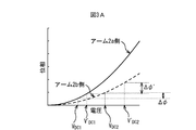
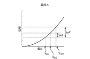
- FIG. 20A shows how the phase changes when a modulation signal is applied to the optical waveguide of the modulator.
- a phase change occurs in a relation of a quadratic function with respect to the modulation signal.
- the efficiency of phase change increases in proportion to the applied DC bias. That is, even when modulated voltage signals having the same amplitude are applied to the optical waveguide, the amount of phase change that occurs depends on the applied DC bias.
- the DC bias applied to the modulation electrodes of the two arms as the optical waveguide is shifted and adjusted. However, when the DC bias is shifted, the reason is as described above.
- the phase change efficiency relationship changes between the two arms.
- the relationship between the voltage applied to the arms 102a and 102b and the phase change is the same.
- a necessary amount of adjustment of the phase difference that is, a necessary difference in DC bias differs depending on each semiconductor MZ optical modulator due to a manufacturing error or the like.
- a necessary amount of phase difference adjustment is ⁇ in a certain modulator.
- the necessary adjustment amount of the phase difference is ⁇ ′, and the phase difference becomes an appropriate value when V DC1 and V DC2 ′.
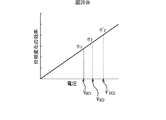
- the phase change efficiency relationship between the arms 102a and 102b differs for each modulator.
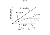
- the efficiency of phase change is the rate of change (differential value) of the phase in FIG. 20A with respect to the DC bias.
- the present invention has been made in view of the above problems, and in a semiconductor MZ type modulator, optimal control of the phase difference between the first and second optical waveguides and precise control of the wavelength chirp characteristics are provided.
- a light modulation device a light modulation device control method, and a light modulation device manufacturing method capable of realizing light modulation having a small device size and good characteristics, which can be realized with a simple element structure. With the goal.
- One aspect of the light modulation device is a light modulation device using a semiconductor Mach-Zehnder type modulator that branches and propagates input light, and combines and outputs the propagated light, the semiconductor Mach-Zehnder
- the modulator includes a first optical waveguide and a second optical waveguide that propagate the branched light, a first electrode that applies a first modulation signal and a first DC bias to the first optical waveguide, A second electrode for applying a second modulation signal and a second DC bias to the second optical waveguide, and the product of the length of the first electrode and the first DC bias;
- the first DC bias and the second DC bias are applied so that the ratio of the product of the length of the two electrodes and the product of the second DC bias is kept constant.
- One aspect of a method for driving an optical modulator is a method for driving an optical modulator using a semiconductor Mach-Zehnder modulator that branches and propagates input light and combines and outputs the propagated light.
- An optical modulation device including a second electrode for applying a second modulation signal and a second DC bias to the optical waveguide of the optical waveguide, the product of the length of the first electrode and the first DC bias;
- the first DC bias and the second optical waveguide are kept in the first optical waveguide and the second optical waveguide so that a ratio of a product of the length of the second electrode and the product of the second DC bias is kept constant. 2 DC bias is applied.
- One aspect of a method for manufacturing a light modulation device is a method for manufacturing a light modulation device using a semiconductor Mach-Zehnder modulator that divides and propagates input light and combines and outputs the propagated light. Forming the first optical waveguide and the second optical waveguide for propagating the branched light when manufacturing the semiconductor Mach-Zehnder modulator, and forming the first optical waveguide on the first optical waveguide.
- a first electrode for applying a first modulation signal and a first DC bias to the optical waveguide; and a second modulation signal and a second signal on the second optical waveguide on the second optical waveguide.
- Forming a second electrode for applying a DC bias and further comprising a product of the length of the first electrode and the first DC bias, the length of the second electrode, and the Maintaining the ratio of the product with the second DC bias at a constant value; Including bias and determining a second DC bias.
- FIG. 1 is a schematic plan view showing a semiconductor MZ modulator used in the light modulation device according to the first embodiment.
- FIG. 1 is a schematic plan view showing a semiconductor MZ modulator used in the light modulation device according to the first embodiment.
- FIG. 2B is
- FIG. 4A is a schematic plan view showing the semiconductor MZ modulator used in the light modulation device according to the first embodiment.
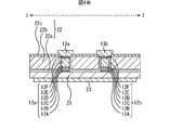
- FIG. 4B is a schematic cross-sectional view showing the semiconductor MZ modulator used in the light modulation device according to the first embodiment.
- FIG. 5 is a schematic plan view showing a modulator module on which the semiconductor MZ modulator of FIGS. 4A and 4B is mounted.
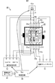
- FIG. 6 is a schematic plan view showing an optical modulation device on which the modulator module of FIG. 5 is mounted.
- FIG. 7 is a schematic plan view illustrating another example of the light modulation device according to the first embodiment.
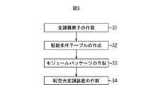
- FIG. 8 is a flowchart showing the method of manufacturing the light modulation device according to the first embodiment in the order of steps.
- FIG. 8 is a flowchart showing the method of manufacturing the light modulation device according to the first embodiment in the order of steps.
- FIG. 10 is a characteristic diagram showing an extinction curve used when adjusting the phase difference in the first embodiment.
- FIG. 11 is a flowchart showing a driving method of the MZ type optical modulation device according to the first embodiment.
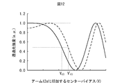
- FIG. 12 is a characteristic diagram showing an extinction curve used when adjusting the phase difference in the second embodiment.
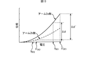
- FIG. 14 is a characteristic diagram showing an extinction curve used when adjusting the phase difference in the third embodiment.
- FIG. 14 is a characteristic diagram showing an extinction curve used when adjusting the phase difference in the third embodiment.
- FIG. 15 is a schematic plan view showing a semiconductor Mach-Zehnder modulator used in the light modulation device according to the fourth embodiment.
- FIG. 16 is a schematic plan view showing a modulator module on which the semiconductor Mach-Zehnder modulator of FIG. 15 is mounted.
- FIG. 17 is a schematic plan view showing an optical modulation device on which the modulator module of FIG. 16 is mounted.
- FIG. 18 is a schematic plan view showing another example of the light modulation device according to the fourth embodiment.
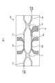
- FIG. 19 is a schematic plan view showing an example of a semiconductor Mach-Zehnder modulator used in a conventional light modulation device.
- FIG. 20A is a characteristic diagram showing a phase relationship with respect to a voltage applied to the optical waveguide of the modulator element.
- FIG. 20B is a characteristic diagram showing the relationship between the efficiency of the phase change with respect to the voltage applied to the optical waveguide of the modulator element.
- FIG. 1 is a schematic plan view showing a semiconductor Mach-Zehnder modulator used in the light modulation device according to the present embodiment.
- the semiconductor MZ type modulator 10 includes a first optical coupler 1, arms 2a and 2b, a semiconductor optical waveguide constituting the second optical coupler 4, and modulation electrodes 3a and 3b.
- the first optical coupler 1 has an input port 1a and is an input coupler that branches incident light into two.
- the arms 2a and 2b are waveguides through which two branched lights propagate.
- the modulation electrodes 3a and 3b are electrodes for applying modulation signals to the arms 2a and 2b, respectively.
- the modulation electrode 3a and the modulation electrode 3b are formed to have different lengths as will be described later.
- the second optical coupler 4 has an output port 4a, and is an output coupler that combines (combines) light propagated through the arms 2a and 2b.
- Each of the two arms 2a and 2b is connected to the first optical coupler 1 at one end and the second optical coupler 4 at the other end.
- the light incident on the first optical coupler 1 from the input port 1a is branched by the arms 2a and 2b, passes through the arms 2a and 2b, respectively, and is multiplexed by the second optical coupler 4 and output from the output port 4a. To do.
- the output light is switched on / off according to the interference state of light at the time of multiplexing. If the phase difference when the light that has passed through the arms 2a and 2b is combined at the output port 4a is 0 (or 2N ⁇ , N is an integer), the interference state is intensifying each other. Is turned on.
- the interference state is mutually debilitating.
- the light enters an off state where no light is output.
- the light incident from the input port 1a is output from the output port 4a with the intensity changed according to the phase difference between the arms 2a and 2b.
- the arm 2a has the first DC bias and the first modulation signal from the modulation electrode 3a
- the arm 2b has the second DC bias from the modulation electrode 3b.
- the second modulation signal are applied.
- the ratio of the product of the length of the modulation electrode 3a and the first DC bias and the product of the length of the modulation electrode 3b and the second DC bias is kept constant.
- a first DC bias and a second DC bias are applied.
- the DC bias refers to a DC bias value at the midpoint of the on / off of the modulation signal, that is, a center bias.
- the efficiency of phase change of the arms 2a and 2b ⁇ 1 and ⁇ 2 are as follows.
- V DC1 and V DC2 are fixed at a constant ratio
- V DC1 : V DC2 A: B
- the ratio of ⁇ 1 and ⁇ 2 is as follows.
- ⁇ 1 : ⁇ 2 AL 1 : BL 2 (4) Since the lengths of the modulation electrodes 3a and 3b are determined when the modulator element 10 is manufactured, L 1 and L 2 are fixed values. Therefore, when the ratio of the DC bias between the two arms is fixed, the ratio of ⁇ 1 and ⁇ 2 , that is, the product of the length L 1 and the first DC bias V DC1 , and the length L 2 And the product of the second DC bias V DC2 is fixed to a constant value.
- the phase value with respect to the center bias is shown in FIGS. 2A and 3A, and the efficiency of the phase change with respect to the center bias is shown in FIGS. 2B and 3B, respectively.
- the efficiency of phase change is the rate of change (differential value) of the phase in FIG. 2A and FIG. 3A relative to the DC bias.
- the modulation electrodes 3a and 3b are formed such that the lengths L 1 and L 2 have a ratio of the amount of phase change (phase change efficiency) suitable for obtaining the optimum chirp characteristics.
- an appropriate chirp characteristic can be obtained by applying the first modulation signal and the second modulation signal having the same amplitude to the arms 2a and 2b by the modulation electrodes 3a and 3b.
- the first and second modulation signals having the same amplitude are applied to the arms 2a and 2b by the modulation electrodes 3a and 3b having the same amplitude to the modulation electrodes 3a and 3b.
- ⁇ parameter ⁇ 0 a chirp characteristic
- the phase change between the arms 2a and 2b is fixed with the ratio of the efficiency of phase change between the arms 2a and 2b fixed. It is possible to adjust the phase difference. As a result, the adjustment of the phase difference between the arms 2a and 2b and the precise control of the chirp characteristics can be performed at the same time. Further, when driving the light modulation device, it is only necessary to adjust the DC bias applied to the modulation electrodes 3a and 3b when adjusting the phase difference. For this reason, it is not necessary to separately provide an electrode for phase control, and the modulator and the modulator module can be downsized.
- FIG. 4A and 4B are schematic views showing a semiconductor Mach-Zehnder modulator used in the optical modulation device according to the first embodiment, in which FIG. 4A is a plan view and FIG. 4B is taken along a broken line II in FIG. 4A. It is sectional drawing.
- FIG. 5 is a schematic plan view showing a modulator module on which the semiconductor Mach-Zehnder modulator of FIG. 4 is mounted.
- FIG. 6 is a schematic plan view showing an optical modulation device on which the modulator module of FIG. 5 is mounted.
- the semiconductor Mach-Zehnder modulator 20 used in the optical modulation device (optical transmitter) according to the present embodiment includes the first optical coupler 11, the arms 12a and 12b, and the second optical coupler 14. And a modulation electrode 13a, 13b.
- the first optical coupler 11 is a so-called 2 ⁇ 2 MMI coupler that has an input port 11a and branches incident light into two.
- the arms 12a and 12b are optical waveguides through which two branched lights propagate.
- the modulation electrodes 13a and 13b are formed on the optical waveguides of the arms 12a and 12b, and are electrodes for applying the first modulation signal and the second modulation signal to the arms 12a and 12b.
- the modulation electrodes 13a and 13b are formed in a so-called traveling wave type microstrip line structure having a portion where a modulation signal is inputted and a portion where the modulation signal is outputted.
- the modulation electrode 13a and the modulation electrode 13b are formed to have different lengths as will be described later.
- the second optical coupler 14 has an output port 14a, and is a 2 ⁇ 2 MMI coupler that multiplexes (combines) light propagated through the arms 12a and 12b.
- the modulation electrodes 13a and 13b are not limited to the microstrip line structure.
- a coplanar electrode structure in which a ground electrode is formed on the upper surface in parallel with the modulation electrode, a lumped constant type electrode, or the like may be used.
- Each of the two arms 12a and 12b has one end connected to the first optical coupler 11 and the other end connected to the second optical coupler 14.
- the light that has entered the first optical coupler 11 from the input port 11a is branched by the arms 12a and 12b, passes through the arms 12a and 12b, and is then combined by the second optical coupler 14 and output from the output port 14a. To do.
- the output light is switched on / off according to the interference state of light at the time of multiplexing. If the phase difference when the light that has passed through the arms 12a and 12b is combined at the output port 14a is 0 (or 2N ⁇ , N is an integer), an interference state that reinforces each other, so that the light is output from the output port 14a. The output is turned on.
- the interference state is mutually debilitating. Is not output.
- the light incident from the input port 11a is output from the output port 14a with the intensity changed according to the phase difference between the arms 12a and 12b.
- the first optical coupler 11, the arms 12a and 12b, and the second optical coupler 14 are formed on the surface of the n-InP substrate 21.
- a waveguide is formed, and an insulating layer 22 is formed so as to cover the side surface of the optical waveguide.
- Modulation electrodes 13a and 13b are formed on the arms 12a and 12b.
- a common ground electrode 23 is formed on the back surface of the n-InP substrate 21.
- the arms 12a and 12b are formed as mesa-structured semiconductor optical waveguides as shown in FIG. 4B.
- the InGaAsP contact layer 12F is sequentially stacked.
- the InGaAsP-MQW core layer 12C is formed, for example, by laminating a plurality of InGaAsP layers and InP layers.
- the insulating layer 22 includes an SiO 2 film 22a formed from the n-InP substrate 21 to the side surfaces of the arms 12a and 12b, a low dielectric resin film 22b formed on the SiO 2 film 22a, and a low dielectric resin film. And an SiO 2 film 22c formed on 22b.
- the SiO 2 films 22a and 22b function as passivation films.
- the low dielectric resin film 22b is formed using, for example, benzocyclobutene (BCB) or the like as a material.
- semiconductor layers 12A to 12F as shown in FIG. 4B are deposited on the n-InP substrate 21 by using, for example, a general MOCVD method. Thereafter, only a portion where the first optical coupler 11, the arms 12a and 12b, the second optical coupler 14, the input port 11a, and the output port 14a are formed is covered by a general lithography technique using a resist and dry etching. A mask such as SiO 2 is formed. Using this mask, the layers 12A to 12F are dry-etched. Thereby, the arms 12a, 12b and the like having a mesa structure are formed.
- the insulating layer 22 is formed on the entire surface by CVD or the like. Then, the insulating layer 22 only on the arms 12a and 12b is removed by a general lithography technique using a resist and dry etching to form an opening. Thereafter, Ti / Pt / Au deposition and gold plating are performed, for example, to form modulation electrodes 13a and 13b connected to the arms 12a and 12b in the openings.
- the InGaAsP-based MQW core layer 12C is used as the optical waveguide core layer.
- the present invention is not limited to this, and other semiconductor MQW core layers such as an AlGaInAs-based MQW core layer may be used.
- the arm 12a in order to adjust the phase of the light passing through the arms 12a and 12b, the arm 12a is supplied with the first DC bias and the first modulation signal from the modulation electrode 13a.
- the second DC bias and the second modulation signal are applied to the arm 12b from the modulation electrode 13b, respectively.
- the ratio of the product of the length of the modulation electrode 13a and the first DC bias and the product of the length of the modulation electrode 13b and the second DC bias is maintained at a constant value.
- a first DC bias and a second DC bias are applied.
- a DC bias (center bias) having the same value and a first modulation signal and a second modulation signal having the same amplitude and opposite voltage changes are applied to the modulation electrodes 13a and 13b.
- the ratio of the efficiency of phase change between the arms 12a and 12b is fixed at the ratio of the lengths of the modulation electrodes 13a and 13b. Accordingly, by appropriately setting the ratio of the modulation electrode length, it is possible to appropriately adjust the ratio of the phase change amount between the two arms and to realize a good negative chirp operation.
- V DC1 : V DC2 is fixed at 1: 1. Accordingly, the phase change efficiency ratio ⁇ 1 : ⁇ 2 in the arms 2 a and 2 b is fixed to the following value.
- ⁇ 1 : ⁇ 2 L 1 V DC1 : L 2
- an optical modulator module 30 is configured using the semiconductor Mach-Zehnder modulator 20 configured as described above.
- the semiconductor Mach-Zehnder modulator 20 is bonded on the carrier 31.
- the carrier 31 on which the semiconductor Mach-Zehnder modulator 20 is mounted is disposed on a temperature adjusting element, for example, a Peltier element 32.
- the Peltier element 32 on which the carrier 31 is mounted is mounted in a module package 33, and the optical modulator module 30 is configured.
- electrodes 31a, 31b, 31c, and 31d are patterned, and a thermistor 38 for monitoring the temperature of the modulator element 20 is provided.
- the electrode 31a is wire-bonded to one end of the modulation electrode 13a
- the electrode 31b is wire-bonded to the other end of the modulation electrode 13a, for example.
- a 50 ⁇ termination resistor 39 connected to the carrier 31 is disposed on the electrode 31b.
- the electrode 31c is wire-bonded to one end of the modulation electrode 13b
- the electrode 31d is wire-bonded to the other end of the modulation electrode 13b, for example.
- a termination resistor 39 connected to the carrier 31 is disposed on the electrode 31d.
- a collimator lens 35 is disposed before and after the semiconductor Mach-Zehnder modulator 20, respectively.
- the module package 33 is provided with optical fibers 34 a and 34 b with lenses for condensing the light that has been collimated by the collimating lens 35.
- the light output from the optical fiber 34a is coupled to the modulator element 20, and the light output through the semiconductor Mach-Zehnder modulator 20 is coupled to the optical fiber 34b.
- the light output from 34b may be coupled to modulator element 20, and the light output after passing through modulator element 20 may be coupled to optical fiber 34a.
- the module package 33 is provided with electrode pins 36a, 36b, 36c, 36d, 37a, 37b, 37c, and 37d for driving the semiconductor Mach-Zehnder modulator 20.
- the electrode pin 36a is wire bonded to the electrode 31a.
- the electrode pin 36 a is electrically connected to one end of the modulation electrode 13 a via the electrode 31 a on the carrier 31.
- the electrode pin 36b is wire-bonded to the ground pattern of the carrier 31 and functions as a ground electrode.
- the electrode pin 36c and the electrode pin 36d are wire bonded to the thermistor 38 and the ground pattern of the carrier 31, respectively.
- the electrode pin 37a is wire bonded to the electrode 31c.
- the electrode pin 37 a is electrically connected to one end of the modulation electrode 13 b through the electrode 31 c on the carrier 31.
- the electrode pin 37b is wire-bonded to the ground pattern of the carrier 31 and functions as a ground electrode.
- the electrode pins 37c and 37d are wire-bonded to the Peltier element 32 to become a positive electrode and a negative electrode, respectively.
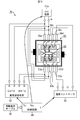
- an optical modulation device 40 is configured using the optical modulator module 30 configured as described above.
- a DC power supply 41a and a high-frequency signal source 42 are connected to the electrode pins 36a and 36b.
- a DC power source 41b and a high-frequency signal source 42 are connected to the electrode pins 37a and 37b.
- a temperature controller 43 is connected to the electrode pins 36c, 36d, 37c, and 37d.
- a control circuit 44 for controlling the DC power sources 41a and 41b, the high-frequency signal source 42, and the temperature controller 43 is provided according to each condition of a drive condition table 45 described later, and the MZ type light modulation device 40 is configured.
- the drive condition table 45 is created at the manufacturing stage of the MZ type light modulation device and stored in a predetermined memory or the like.
- the DC power supply 41 a applies the first DC bias V DC1 described in the drive condition table 45 between the electrode pins 36 a and 36 b under the control of the control circuit 44.
- RF signal source 42 is controlled by the control circuit 44 applies a first modulated signal is a high frequency signal amplitude V pp described in the driving condition table 45 electrode pins 36a, between 36b.
- the DC power supply 41 b applies the second DC bias V DC2 described in the drive condition table 45 between the electrode pins 37 a and 37 b under the control of the control circuit 44.
- RF signal source 42 is controlled by the control circuit 44 applies a second modulated signal is a high frequency signal amplitude V pp described in the driving condition table 45 electrode pins 37a, between 37b.
- the modulation electrode 13a has the first DC bias V DC1 and the first modulation signal
- the modulation electrode 13b has the second DC bias V DC2 and the second modulation signal.
- the first modulation signal and the second modulation signal are modulation signals having the same amplitude and opposite voltage changes.
- the temperature controller 43 measures the resistance of the thermistor 38 to observe the temperature of the modulator element 20, adjusts the current injected into the Peltier element 32 based on the observed temperature, and adjusts the temperature of the modulator element 20. adjust.
- the modulator element 20 adjusts the driving temperature T described in the driving condition table 45 under the control of the control circuit 44.
- the first DC bias V DC1 and the second DC bias V DC2 are set to the same value by the control of the control circuit 44 based on the drive condition table 45. Therefore, as shown in FIG. 7, the DC power supply 41b may be omitted, and only the DC power supply 41a may be provided. In this case, the DC power supply 41a is connected to the electrode pins 36a and 36b and the electrode pins 37a and 37b. DC power supply 41a is controlled by the control circuit 44 applies a DC bias V DC which is described in the drive condition table 45 electrode pins 36a, 36b and between the electrode pins 37a, between 37b. At this time, the DC bias VDC having the same value is applied to the modulation electrodes 13a and 13b.
- FIG. 8 is a flowchart showing the method of manufacturing the MZ type light modulation device 40 in the order of steps.
- a modulator element is manufactured (step 1).
- the process of Step 1 is as described above and is omitted here.
- the characteristics of the semiconductor Mach-Zehnder modulator for creating the drive condition table 45 are evaluated, and the drive condition table 45 is created (step S2).
- V DC1 , V DC2 , and V pp are values that can perform a favorable modulation operation in a state where the semiconductor Mach-Zehnder modulator 20 is adjusted to the driving temperature T.
- step S3 the optical modulator module 30 is produced (step S3).
- the semiconductor Mach-Zehnder modulator 20 is bonded onto the carrier 31, the carrier 31 is disposed on the Peltier element 32, and the Peltier element 32 is mounted in the module package 33.
- the step S2 for creating the drive condition table 45 may be executed after the optical modulator module 30 is produced in step S3.
- step S4 the MZ type light modulation device 40 is manufactured (step S4).
- DC power sources 41 a and 41 b, a high-frequency signal source 42, and a temperature controller 43 are connected to the optical modulator module 30, and a control circuit 44 is connected.
- the control circuit 44 is connected to a memory in which a driving condition table 45 is stored.
- step S2 for creating the drive condition table 45 will be described in detail.
- the first and second modulation signals are applied to the modulation electrodes 13a and 13b of the arms 12a and 12b as in the present embodiment so that the voltage changes are opposite to each other.
- the first modulation signal applied to the modulation electrode 13a is on level (higher voltage level)
- the second modulation signal applied to the modulation electrode 13b is off level (lower voltage level).
- the light signal level is set to the on level.
- the first modulation signal is off level and the second modulation signal is on level
- the light signal level is set to off level.
- the light input port is the upper 11a and the output port is the lower 14a
- the light that has passed through the arms 12a and 12b passes through the output port 14a.
- the phase difference at the time of multiplexing is 0 (or 2N ⁇ , N is an integer)
- light is output from the lower output port 14a. Therefore, the light signal level is turned on.
- the phase difference when the light that has passed through the arms 12a and 12b is combined at the output port 14a is ⁇ (or (2N + 1) ⁇ )
- the light is output from the upper output port and from the lower output port. Is hardly output. Therefore, the light signal level is turned off.
- phase difference it is necessary to adjust the phase difference between the arms 12a and 12b so that the phase difference is 2N ⁇ when the first modulation signal is on level and the second modulation signal is off level.
- the phase difference needs to be (2N + 1) ⁇ when the first modulation signal is off level and the second modulation signal is on level.
- the phase difference needs to be approximately (2N + 0.5) ⁇ at the center bias that is the center value of the on level and the off level of the first and second modulation signals.
- the input port is set to the upper side 11a and the output port is set to the lower side. 14a
- the phase difference of the light that has passed through the arms 12a and 12b is zero when no voltage is applied to the modulation electrodes 13a and 13b.
- the phase difference is not exactly 0 but has a finite value ⁇ due to a manufacturing error or the like. Since this ⁇ is caused by a manufacturing error or the like, even if the semiconductor Mach-Zehnder modulator 20 having the same specification is manufactured, each semiconductor Mach-Zehnder modulator 20 has a different value.
- the initial phase difference between the arms 12a and 12b due to this manufacturing error is taken into consideration. It needs to be put in. That is, the amount of phase difference between the arms 12a and 12b generated by applying a DC bias needs to be (2N + 0.5) ⁇ .
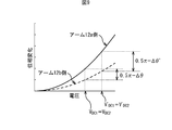
- FIG. 9 shows a rewritten version of FIG. 2 for explaining a driving method for adjusting the phase difference by increasing / decreasing the DC bias.
- the DC bias is increased or decreased in a state where the DC bias is matched between the arms 12a and 12b.
- the lengths of the modulation electrodes 13a and 13b are different, even if the same voltage is applied, the arms 12a and 12b The amount of phase change that occurs is different.
- the phase difference between the arms 12a and 12b also changes by increasing or decreasing the center bias value.
- the phase difference between the arms 12a and 12b increases.
- the phase difference between the arms 12a and 12b can be appropriately adjusted.
- the initial phase difference is ⁇ ′ in another modulator element 20
- the DC bias of the arms 12a and 12b is set to V ′ in FIG. 9 so that the phase difference becomes a value of 0.5 ⁇ ′. Just do it.
- the required DC bias value is different for each modulator element 20.
- the ratio of the amount of phase change generated in the arms 12a and 12b can be fixed regardless of the DC bias value. For this reason, the characteristics of the wavelength chirp are hardly changed. As a result, it is possible to achieve both proper control of the phase difference between the arms 12a and 12b and precise control of the wavelength chirp, and good modulation characteristics can be obtained in the modulator element 20.
- step S1 the phase difference is adjusted by the following procedure to create a DC bias driving condition table.
- the first DC bias or the second DC bias
- the first DC bias is changed (swept) from 0 V to several V in a state where the first DC bias and the second DC bias applied to the modulation electrodes 13a and 13b are matched.
- the intensity of the light output from the output port in this case, the output port 14a
- a so-called extinction curve as shown in FIG. 10 is obtained.
- This extinction curve represents a state in which the state of interference changes due to the phase difference between the arms and the output light intensity changes.
- the phase difference between the arms 12a and 12b is 2N ⁇ at the maximum portion and (( 2N + 1) ⁇ .
- the phase difference between the arms 12a and 12b is (2N + 0.5) ⁇ when the center bias V cb that is the midpoint between the maximum and minimum is applied. Therefore, the above-described phase adjustment is performed by matching the center bias V cb with the first DC bias applied to the arm 12a.
- the second DC bias applied to the arm 12b is also set to the center bias V cb. It ’s fine.
- this extinction curve is a solid line in FIG. 10 when the initial phase difference between the arms 12a and 12b is zero. As shown, the extinction curve reaches a local maximum when the bias is zero. When there is a manufacturing error in the modulator element 20 and there is an initial phase difference generated thereby, the extinction curve shifts in the horizontal axis direction as shown by the broken line in FIG. To have.
- the DC bias applied to the arm 12a may be set to the value of the center bias V cb in FIG.
- the first DC bias V DC1 applied to the arm 12a may be set to the value of the center bias V cb ′ in FIG.
- the center bias that is the middle point between the maximum and minimum is changed due to the initial phase difference generated depending on the manufacturing variation of the semiconductor Mach-Zehnder modulator 20, the DC bias whose phase is appropriately adjusted can be obtained. Different for each semiconductor Mach-Zehnder modulator 20.
- the determined V DC1 and V DC2 are written in the drive condition table 45 together with the drive temperature T.
- the phase change of the waveguide when a voltage is applied is very little deteriorated with time. Therefore, if a drive condition table is created as described above at the manufacturing stage and the semiconductor Mach-Zehnder modulator 20 is driven based on the table, it is possible to maintain a good modulation operation semi-permanently.
- an MZ type optical modulator be operable over the entire C-band band of the communication wavelength band, for example.
- the MZ type optical modulator has different characteristics for each wavelength due to the wavelength dependence of the amount of phase change when a voltage is applied to the semiconductor optical waveguide.
- the condition of the DC bias having the optimal phase as described above varies depending on the wavelength. Therefore, it is basically necessary to separately evaluate the DC bias condition for each wavelength. Since the in-phase DC bias has a relatively simple relationship with the wavelength, the extinction curve is evaluated at several wavelengths to obtain the optimum value of the DC bias, and the evaluated wavelength is based on the result. What is necessary is just to obtain
- the DC bias may be adjusted by evaluating the extinction curve as described above at the three wavelengths of the short-wave side and the long-wave side end and center of the C-band. For the DC bias at the wavelength between the adjusted wavelengths, the condition of the DC bias at all wavelengths is compensated by using linear interpolation or complementing the relationship between the DC bias and the wavelength with a quadratic function. Just ask.
- the first and second extinction ratios can be obtained under the condition that the first and second DC biases V DC1 and V DC2 are set to the center bias V bc obtained at each wavelength as described above.
- the amplitude (V pp ) of the second modulation signal is determined in advance. Then, the determined Vpp is described in the drive condition table 45.
- the amplitude of the first and second modulation signals may be adjusted by, for example, observing the eye pattern of the modulation waveform and determining V pp that is large enough to ensure a sufficient extinction ratio.
- the optimum value differs for each wavelength in the semiconductor Mach-Zehnder modulator 20. In this case, as in the determination of the first and second DC biases V DC1 and V DC2 , the optimum V pp is experimentally obtained at several wavelengths, and the wavelength between them is complemented by a simple relationship. .
- FIG. 11 is a flowchart showing a method of driving the light modulation device according to the first embodiment.
- the control circuit 44 reads the driving temperature T of the semiconductor Mach-Zehnder modulator 20 from the driving condition table 45 (step S11).
- the temperature controller 43 adjusts the temperature of the semiconductor Mach-Zehnder modulator 20 to a constant driving temperature T (for example, 25 ° C.) under the control of the control circuit 44 (step S12).
- the control circuit 44 reads the first and second DC biases V DC1 and V DC2 to be applied to the arms 12a and 12b from the drive condition table 45 (step S13).
- the DC power sources 41a and 41b read the first and first read into the modulation electrodes 13a and 13b of the arms 12a and 12b via the electrode pins 36a and 36b and the electrode pins 37a and 37b. 2 DC biases V DC1 and V DC2 are applied (step S14).
- the control circuit 44 reads the amplitude V pp of the high frequency signal from the drive condition table 45 (step S15).
- the high-frequency signal source 42 is controlled by the control circuit 44 with the amplitude V pp read into the modulation electrodes 13a and 13b of the arms 12a and 12b via the electrode pins 36a and 36b and the electrode pins 37a and 37b.
- First and second modulation signals which are high-frequency signals whose voltage changes are opposite to each other, are applied (step S16). With the above procedure, the modulator element 20 can perform a good modulation operation.
- the case where 2 ⁇ 2 MMI couplers are used as the input and output optical couplers has been described as the structure of the semiconductor Mach-Zehnder modulator 20, but the structure is not limited to this.
- the input-side optical coupler may be any one that can split the input light into two
- the output-side optical coupler may be any one that couples the light incident from the two arms.
- the same effect can be obtained with an optical coupler using a 1 ⁇ 2 MMI coupler, a Y-branch coupler, or a directional coupler.
- the ideal phase difference that occurs when no DC bias is applied differs depending on the combination of optical couplers used, and the DC bias needs to be adjusted accordingly.
- the phase difference between the arms when no voltage is applied to the modulation electrode is ideally 0.5 ⁇ . It becomes. Therefore, it may be considered that the necessary phase adjustment amount is only the initial phase difference generated due to a manufacturing error or the like.
- the present embodiment is directed to an optical modulation device using a semiconductor Mach-Zehnder modulator, as in the first embodiment, it is different in that the modulation mode is different.
- the configurations of the semiconductor Mach-Zehnder modulator, the light modulator module, and the light modulation device are substantially the same as those of the first embodiment. Therefore, also in this embodiment, it demonstrates using the drawing and code
- the arm 12a In order to perform the modulation operation by changing the phase of the light passing through the arms 12a and 12b, the arm 12a is supplied with the first DC bias and the first modulation signal from the modulation electrode 13a, and the arm 12b is supplied with the modulation electrode 13b. A second DC bias and a second modulation signal are applied, respectively.
- the ratio of the product of the length of the modulation electrode 13a and the first DC bias and the product of the length of the modulation electrode 13b and the second DC bias is maintained at a constant value.
- a first DC bias and a second DC bias are applied.
- the arms 12a and 12b change in phase by approximately the same amount in opposite directions, and a satisfactory zero chirp operation can be realized.
- V DC1 : V DC2 is fixed at 1: 3. Accordingly, the ratio ⁇ 1 : ⁇ 2 of the phase change efficiency in the arms 12a and 12b is fixed to the following value.
- the first and second DC biases are increased or decreased in the arms 12a and 12b while the relationship of the first DC bias V DC1 : second DC bias V DC2 is fixed to 1: 3.
- the phase difference between the arms 12a and 12b can be changed and adjusted.
- the first and second DC biases when the first and second DC biases are increased, the phase difference increases, so that the phase difference between the arms 12a and 12b can be optimally adjusted.
- the phase difference is adjusted by the following procedure.
- the first DC bias is changed from 0 V to several V with the relationship between the first and second DC biases V DC1 and V DC2 applied to the modulation electrodes 13a and 13b fixed at 1: 3.
- an extinction curve as shown in FIG. 12, for example, is obtained.
- the above-described phase adjustment is performed by matching the center bias V cb of FIG. 12 with the first DC bias applied to the arm 12a.
- the second DC bias applied to the arm 12b is A value of V cb ⁇ 3 may be used.
- this extinction curve is zero when the initial phase difference between the arms 12a and 12b is zero as shown by the solid line in FIG. By the way, it becomes maximum value. If there is a manufacturing error in the modulator element 20 and there is an initial phase difference generated thereby, the extinction curve shifts in the horizontal axis direction as shown by a broken line in FIG. It becomes like this.
- the first DC bias applied to the arm 12a may be set to the value of the center bias V cb in FIG.
- the first DC bias V DC1 applied to the arm 12a may be set to the value of the center bias V cb ′ in FIG.
- the method of driving the light modulation device according to the present embodiment is the same as that in FIG. 11 of the first embodiment. That is, in steps S11 to S14, the drive temperature T is read from the drive condition table to adjust the temperature, V DC1 and V DC2 are read and applied to the modulation electrodes 13a and 13b, and the amplitude V pp is read to change the voltage between each other. Apply a high-frequency signal that is reversed.
- the present embodiment is directed to an optical modulation device using a semiconductor Mach-Zehnder modulator, as in the first embodiment, it is different in that the modulation mode is different.
- the configurations of the semiconductor Mach-Zehnder modulator, the light modulator module, and the light modulation device are substantially the same as those of the first embodiment. Therefore, also in this embodiment, it demonstrates using the drawing and code
- the arm 12a In order to perform the modulation operation by changing the phase of the light passing through the arms 12a and 12b, the arm 12a is supplied with the first DC bias and the first modulation signal from the modulation electrode 13a, and the arm 12b is supplied with the modulation electrode 13b. A second DC bias and a second modulation signal are applied, respectively.
- the ratio of the product of the length of the modulation electrode 13a and the first DC bias and the product of the length of the modulation electrode 13b and the second DC bias is maintained at a constant value.
- a first DC bias and a second DC bias are applied.
- the above-described ratio in the first and second modulation signals is maintained at 5: 1, for example.
- the ratio of the length of the modulation electrodes 13a L 1 and the length L 2 of the modulation electrode 13b is 2: to be 1, to form the modulation electrode 13a, a 13b.
- ⁇ 1 : ⁇ 2 of the phase change efficiency in the arms 12a and 12b is fixed to the following value.
- ⁇ 1 5: 1
- a 5: 1 phase change occurs in the directions opposite to each other in the arms 12a and 12b, and a favorable negative chirp operation can be realized.
- the first and second DC biases are increased or decreased in the arms 12a and 12b while the relationship of the first DC bias V DC1 : second DC bias V DC2 is fixed at 2.5: 1.
- the phase difference between the arms 12a and 12b can be changed and adjusted.
- the phase difference between the arms 12 a and 12 b is ⁇
- the first and second DC biases are V DC1 ′ and V DC2 ′
- the phase difference is ⁇ ′.
- the phase difference increases, so that the phase difference between the arms 12a and 12b can be optimally adjusted.
- the phase difference is adjusted by the following procedure.
- the relationship between the first and second DC biases V DC1 and V DC2 applied to the modulation electrodes 13a and 13b fixed at 2.5: 1 the second DC bias is changed from 0V to several volts.
- the intensity of the light output from the output port in this case, the output port 14a
- an extinction curve as shown in FIG. 14 is obtained.
- the above-described phase adjustment is performed by matching the center bias V cb of FIG. 14 with the second DC bias applied to the arm 12b.
- the first DC applied to the arm 12a since the relationship between the first and second DC biases V DC1 and V DC2 applied to the modulation electrodes 13a and 13b is fixed at 2.5: 1, the first DC applied to the arm 12a.
- the bias may be a value of V cb ⁇ 2.5.
- the extinction curve is zero when the initial phase difference between the arms 12a and 12b is zero as shown by the solid line in FIG. By the way, it becomes maximum value.
- the extinction curve shifts in the horizontal axis direction as shown by the broken line in FIG. It becomes like this.
- the second DC bias applied to the arm 12b may be set to the value of the center bias V cb in FIG.
- the second DC bias V DC1 applied to the arm 12b may be set to the value of the center bias V cb ′ in FIG.
- V DC1 2.5V DC2 in this embodiment
- the first and second modulation signal amplitude V pp and drive temperature T it is described in the driving condition table.
- the driving method of the MZ type light modulation device according to the present embodiment is the same as that in FIG. 11 of the first embodiment. That is, in steps S11 to S14, the drive temperature T is read from the drive condition table to adjust the temperature, V DC1 and V DC2 are read and applied to the modulation electrodes 13a and 13b, and the amplitude V pp is read to change the voltage between each other. Apply a high-frequency signal that is reversed.
- FIG. 15 is a schematic plan view showing a semiconductor Mach-Zehnder modulator used in the light modulation device according to the fourth embodiment.
- FIG. 16 is a schematic plan view showing a modulator module on which the semiconductor Mach-Zehnder modulator of FIG. 15 is mounted.
- FIG. 17 is a schematic plan view showing an optical modulation device on which the modulator module of FIG. 16 is mounted.
- the semiconductor Mach-Zehnder modulator 50 used in the optical modulation device (optical transmitter) includes the first optical coupler 11, the arms 12a and 12b, and the second optical coupler 14. It comprises a semiconductor optical waveguide and modulation electrodes 13a and 13b.
- the first optical coupler 11, the arms 12a and 12b, and the second optical coupler 14 are the same as those of the modulator element 20 of the first embodiment.
- the cross-sectional configurations of the arms 12a and 12b are also the same as in FIG. 4B of the first embodiment.
- the modulation electrodes 13a and 13b are formed to have the same length.
- the additional electrode 51 is formed only on the arm 12b.
- the additional electrode 51 is formed by patterning simultaneously with the modulation electrodes 13a and 13b.
- the first modulation signal and the second modulation signal from the modulation electrodes 13a and 13b are applied to the arms 12a and 12b.
- the ratio of the product of the second DC bias V DC2 is kept constant.
- “the length of the additional electrode” is the same as the “length of the modulation electrode” in the longitudinal direction of the arm of the portion electrically connected to the waveguide constituting the arm of the additional electrode. Say the length along.
- an optical modulator module 60 is configured using the semiconductor Mach-Zehnder modulator 50 configured as described above.
- the optical modulator module 60 is configured in substantially the same manner as the optical modulator module 30 of FIG. 5 of the first embodiment except for the semiconductor Mach-Zehnder modulator 50, but an electrode 31e and an inductor 52 are attached to the carrier 31. Is different.
- the electrode 31e is wire-bonded to one end of the additional electrode 51.
- the inductor 52 is, for example, about 100 ⁇ H, and is provided so as to electrically connect the electrode 31d and the electrode 31e.
- the module package 33 is not provided with an electrode pin for applying a voltage independently to the additional electrode 51. Therefore, in the present embodiment, forming the additional electrode 51 does not increase the number of electrode pins.
- an optical modulator 70 is configured using the optical modulator module 60 configured as described above.
- the light modulation device 70 is configured in substantially the same manner as the light modulation device 40 of FIG. 6 of the first embodiment except for the light modulator module 60.
- the DC power sources 41a and 41b and the high-frequency signal source 42 cause the modulation electrode 13a to have the first DC bias and the first modulation signal, and the modulation electrode 13b to have the second DC bias and the second DC signal.
- Each modulation signal is applied.
- the second DC bias is applied to both the modulation electrode 13b and the additional electrode 51.
- the second modulation signal which is a high-frequency signal, is hardly applied to the additional electrode 51 by the inductor 52.
- the first and second DC biases applied to the modulation electrodes 13a and 13b are matched by the arms 12a and 12b, and the first and second modulation signals applied to the modulation electrodes 13a and 13b are The amplitudes are equal and the direction of voltage change is reversed.
- the efficiency of phase change with respect to the first and second modulation signals is equal between the arms 12a and 12b.
- a zero chirp operation in which the amount of phase change is equal between the arms 12a and 12b is realized.
- the first and second biases are applied to the electrodes having different effective lengths. Will do. Therefore, as in the first embodiment, the phase difference between the arms 12a and 12b can be adjusted by increasing or decreasing the first and second DC biases while keeping them equal to each other.
- the phase difference between the arms 12a and 12b can be optimally adjusted while maintaining the zero chirp operation. Further, since the amplitudes of the first and second modulation signals to be applied are the same in the arms 12a and 12b, and the magnitudes of the first and second DC bias to be applied are the same in the arms 12a and 12b, it is simple. Control can be performed.
- the first DC bias V DC1 and the second DC bias V DC2 are set to the same value by the control of the control circuit 44 based on the drive condition table 45. Therefore, as shown in FIG. 18, the DC power supply 41b may be omitted, and only the DC power supply 41a may be provided. In this case, a DC power supply 41a is connected between the electrode pins 36a and 36b and between the electrode pins 37a and 37b. DC power supply 41a is controlled by the control circuit 44 applies a DC bias V DC which is described in the drive condition table 45 electrode pins 36a, 36b and between the electrode pins 37a, between 37b. At this time, the same value of DC bias VDC is applied to the modulation electrode 13a, the modulation electrode 13a, and the additional electrode 51.
- V DC1 and V DC2 when the ratio between the first DC bias V DC1 and the second DC bias V DC2 is a constant value, V DC1 and V DC2 that are single constant values are used. It has been described in the drive condition table, and the mode in which the light modulation device is driven based on this is shown. Other aspects can be considered in this regard.
- V DC1 and V DC2 which are 5: 1 are described. Then, depending on the use state of the MZ type light modulation device, appropriate V DC1 and V DC2 may be read from the drive condition table to obtain a desired 0 chirp operation or negative chirp operation.
Landscapes
- Physics & Mathematics (AREA)
- Nonlinear Science (AREA)
- General Physics & Mathematics (AREA)
- Optics & Photonics (AREA)
- Chemical & Material Sciences (AREA)
- Engineering & Computer Science (AREA)
- Ceramic Engineering (AREA)
- Crystallography & Structural Chemistry (AREA)
- Optical Modulation, Optical Deflection, Nonlinear Optics, Optical Demodulation, Optical Logic Elements (AREA)
Abstract
アーム(12a,12b)を通過する光の位相を調整する際に、アーム(12a)には変調電極(13a)から第1のDCバイアス及び第1の変調信号を、アーム(12b)には変調電極(13b)から第2のDCバイアス及び第2の変調信号をそれぞれ印加し、第1及び第2のDCバイアスは、変調電極(13a)の長さと第1のDCバイアスとの積と、変調電極(13b)の長さと第2のDCバイアスとの積との比率を一定値に保つように、変調電極(13a,13b)に印加される。この構成により、半導体マッハ・ツェンダ変調器を用いた光変調装置において、アーム(12a,12b)間の位相差の最適な制御と、精密な波長チャープ特性の制御とを、簡素な素子構造で実現することが可能となり、装置サイズが小型で且つ良好な特性を持つ光変調が実現される。
Description
本発明は、マッハ・ツェンダ型の光導波路を備えた光変調装置、その駆動方法、及びその製造方法に関する。
大容量の光通信が可能であるWDMシステムの通信用光源として強く求められている、広い波長範囲で高速に動作する光変調装置として、いわゆるマッハ・ツェンダ(Mach-Zehnder)型変調器を用いた光変調装置が注目されている。現在、長距離及び大容量の光通信システムにおいては、例えば非線形光学結晶ニオブ酸リチウム(LiNbO3,LN)中の電気光学効果を利用したマッハ・ツェンダ干渉計型光変調器(以下、単にLN-MZ型光変調器と称する。)と半導体レーザとを備えた光送信機が用いられている。また近年では、小型化が可能な半導体マッハ・ツェンダ(MZ)型光変調器(以下、単に半導体MZ型光変調器と称する。)及び半導体MZ型光変調器集積型の半導体レーザの開発が進められている。
半導体MZ型光変調器の一例を図19に示す。
この半導体MZ型変調器は、半導体導波路で形成される第1の光カプラ101、アーム102a,102b、第2の光カプラ104及び変調電極103a,103bを備えて構成される。
第1の光カプラ101は、入力ポート101aを有しており、入射光を2つに分岐する入力カプラである。アーム102a,102bは、2本の分岐された光が伝播する導波路である。変調電極103a,103bは、アーム102a,102bの導波路上に形成されており、アーム102a,102bにそれぞれ変調信号を印加するための電極である。第2の光カプラ104は、出力ポート104aを有しており、アーム102a,102bを伝播した光を合波(結合)する出力カプラである。
この半導体MZ型変調器は、半導体導波路で形成される第1の光カプラ101、アーム102a,102b、第2の光カプラ104及び変調電極103a,103bを備えて構成される。
第1の光カプラ101は、入力ポート101aを有しており、入射光を2つに分岐する入力カプラである。アーム102a,102bは、2本の分岐された光が伝播する導波路である。変調電極103a,103bは、アーム102a,102bの導波路上に形成されており、アーム102a,102bにそれぞれ変調信号を印加するための電極である。第2の光カプラ104は、出力ポート104aを有しており、アーム102a,102bを伝播した光を合波(結合)する出力カプラである。
2本のアーム102a,102bは、それぞれ一端が第1の光カプラ101と、他端が第2の光カプラ104と接続されている。入力ポート101aから第1の光カプラ101に入射した光は、アーム102a,102bで分岐し、それぞれアーム102a,102bを通過した後に、第2の光カプラ104で合波されて出力ポート104aから出力する。この合波時における光の干渉状態により、出力光のオン/オフが切り替えられる。アーム102a,102bを通過した光が第2の光カプラ104の出力ポート104aにおいて再び結合する際の位相差が0(又は2Nπ,Nは整数)の場合には、互いに強め合う干渉状態となるため、出力ポート104aから光が出力されるオン状態となる。一方、アーム102a,102bを通過した光が第2の光カプラ104の出力ポート104aにおいて再び結合する際の位相差がπ(又は(2N+1)π)の場合には、互いに弱め合う干渉状態となるため、出力ポート104aから光が出力されないオフ状態となる。
アーム102a,102bを通過する光の位相の調整方法としては、例えば、アーム102a,102bに電界を印加したときに生じる屈折率変化を利用して位相を調整する方法等がある。従って、変調電極103a,103bによりアーム102a,102bに変調電圧信号を印加すれば、変調電圧信号に応じてアーム102a,102bで位相の変化が起こり、結果として出力される光の強度が変調される。良好な光変調を行うためには、先ず、アーム102a,102bに印加する変調信号が、位相差をπだけ変化させるのに十分大きな振幅を持つ必要がある。それに加えて、変調電圧信号のオフレベルにおいて位相差がπとなり、オンレベルにおいて位相差が0となるように、アーム102a,102bを通過した光の位相差を制御することが必要である。アーム102a,102bを通過する光の位相差は、製造誤差等に依存して各々の変調器素子ごとに異なるため、変調器素子ごとに位相を調整する必要がある。
アーム102a,102b間の位相差を制御する方法としては、変調電極103a,103bとは別に位相制御用の電極を少なくとも一方のアームに形成し、この位相制御用の電極に印加する電圧を調整して少なくともどちらか一方のアームの屈折率を変化させ、位相を変える方法がある。アーム102a,102b間の位相差を制御する別の方法としては、変調電極103a,103bに印加するDCバイアスに差をつける方法がある。一般的に半導体MZ型変調器では、数V程度のDCバイアスを印加して変調動作を行うが、このDCバイアスをアーム102a,102b間で差を付けることによって、アーム102a,102b間の位相差を調整することができる。
一方、MZ型光変調器では、変調時に出力光の波長が変動する、いわゆる波長チャープという現象が生じる。この波長チャープは、光ファイバ伝送後の光変調波形が劣化する要因となる。そのため、MZ型光変調器において十分な変調特性を得るためには、波長チャープを精密に制御する必要がある。波長チャープの制御技術としては、波長チャープの量を極力小さくするゼロチャープ動作の技術、伝送後の光波形に改善が見られるような波長チャープを意図的に付加する負チャープ動作の技術がある。これらのチャープ制御技術は、変調電圧信号を印加した場合に、アーム102a,102bにおいて発生する光の位相変化の振幅の比率を調整することによって実現される。ゼロチャープ動作では、高周波電圧である変調信号を印加した場合にアーム102a,102bにおいて発生する光の位相変化の振幅の比率を1:1に固定することが望ましい。負チャープ動作では、一方のアームと他方のアームとにおいて発生する光の位相変化の振幅の比率を、例えば0.85:0.15程度に固定することが望ましい。
上記の比率は、例えば、アーム102a,102bに印加される電圧信号の振幅の比率を調整することにより実現される。ゼロチャープ動作を実現するには、アーム102a,102bに振幅が同じで且つ方向が逆となるような変調信号を印加し、アーム102a,102bで発生する位相変化の量が同じで且つ方向が逆になるようにする。負チャープ動作を実現するには、例えば、アーム102a,102bで振幅の大きさが異なり、且つ方向が逆となる変調信号を印加し、アーム102a,102bのうちで片方の位相変化量が多くなるようにする。
以上のように、MZ型光変調装置では、良好な変調特性を得るためには、アーム102a,102b間における位相差の制御及びアーム間の位相変化の振幅の比率の制御の双方を適切に行うことが要求される。
以上のように、MZ型光変調装置では、良好な変調特性を得るためには、アーム102a,102b間における位相差の制御及びアーム間の位相変化の振幅の比率の制御の双方を適切に行うことが要求される。
近年、上記のような半導体MZ変調器を搭載した光送受信機モジュールの小型化が強く求められている。
上記のような光送受信機モジュールの小型化には、変調器自身が小さいことが先ず必要である。また、変調器の小型化だけではなく、変調器を含む変調器モジュールの小型化、簡素化が重要となる。この場合、前述した位相の制御方法のうち、変調電極とは別に位相制御用の電極を用いる方法では、変調器モジュールにおける接続用の電極ピンの数が増えることになり、小型化には不向きである。また、位相制御用の電極の付加に伴って変調器の制御パラメータが1つ増えることになるため、制御回路の構成が複雑になるという問題もある。
上記のような光送受信機モジュールの小型化には、変調器自身が小さいことが先ず必要である。また、変調器の小型化だけではなく、変調器を含む変調器モジュールの小型化、簡素化が重要となる。この場合、前述した位相の制御方法のうち、変調電極とは別に位相制御用の電極を用いる方法では、変調器モジュールにおける接続用の電極ピンの数が増えることになり、小型化には不向きである。また、位相制御用の電極の付加に伴って変調器の制御パラメータが1つ増えることになるため、制御回路の構成が複雑になるという問題もある。
DCバイアスを変調電極に印加する位相の調整方法について考察する。この場合、半導体MZ型光変調器のパッケージの小型化等には適しているが、以下に説明するように、波長チャープの制御が困難であるという半導体MZ型変調器に特有の問題がある。
半導体MZ型光変調器では、一般的に、光導波路に逆電圧の変調信号を印加して屈折率を変化させて変調動作を実現する。ここで逆電圧の変調信号の印加とは、半導体MZ型光変調器のp側電極に負のバイアスを、n側電極に正のバイアスをそれぞれ印加することを意味する。以降、光導波路に逆電圧を印加することを、単に電圧を印加すると記載する。
半導体MZ型光変調器では、一般的に、光導波路に逆電圧の変調信号を印加して屈折率を変化させて変調動作を実現する。ここで逆電圧の変調信号の印加とは、半導体MZ型光変調器のp側電極に負のバイアスを、n側電極に正のバイアスをそれぞれ印加することを意味する。以降、光導波路に逆電圧を印加することを、単に電圧を印加すると記載する。
変調器の光導波路に変調信号を印加した場合の位相変化の様子を図20Aに示す。図示のように、光導波路では、変調信号に対してほぼ二次関数の関係で位相変化が生じる。換言すれば、印加するDCバイアスにほぼ比例して、位相変化の効率が高くなる。即ち、同じ振幅の変調電圧信号を光導波路に印加した場合でも、印加されているDCバイアスに依存して発生する位相変化量が変化する。
変調器において、DCバイアスにより位相差を調整する場合には、光導波路である2本のアームの変調電極に印加するDCバイアスをずらして調整するが、DCバイアスをずらすと上記のような理由で2本のアームの間で位相変化の効率の関係が変化する。
変調器において、DCバイアスにより位相差を調整する場合には、光導波路である2本のアームの変調電極に印加するDCバイアスをずらして調整するが、DCバイアスをずらすと上記のような理由で2本のアームの間で位相変化の効率の関係が変化する。
図19のような、変調電極103a,103bの長さが同じである変調器の場合では、アーム102a,102bに印加した電圧と位相変化の関係は同じである。必要な位相差の調整量、即ち必要なDCバイアスの差は、製造誤差等により各々の半導体MZ光変調器で異なる。例えば図20Aのように、ある変調器では必要な位相差の調整量がΔφであるとする。このとき、アーム102a,102bに印加するDCバイアスがVDC1,VDC2のときに位相差が適切な値になる。これに対して、別の変調器では、必要な位相差の調整量がΔφ’であり、VDC1,VDC2’のときに位相差が適切な値になる。
その結果、図20Bに示すように、アーム102a,102b間における位相変化の効率の関係は、変調器ごとで異なるものとなる。図20Bにおいて、位相変化の効率とは、図20Aにおける位相のDCバイアスに対する変化率(微分値)である。
その結果、図20Bに示すように、アーム102a,102b間における位相変化の効率の関係は、変調器ごとで異なるものとなる。図20Bにおいて、位相変化の効率とは、図20Aにおける位相のDCバイアスに対する変化率(微分値)である。
背景技術において示したように、波長チャープの制御には2つのアーム(導波路)で発生する位相変化量の比率を精密に調整する必要がある。上記のようにDCバイアスで位相制御を行った場合には、2つのアーム間の電圧信号に対する位相変化の効率にずれが生じ、MZ光変調器ごとにアーム間の位相変化の振幅の比率が変わってしまう。そのため、2つのアームで発生する位相変化量の比率を精密に調整することができず、良好なチャープ特性を得ることができなくなる。
位相変化の効率の変化分について、変調信号の大きさの比率を変えることにより、位相変化量を調整することも考えられる。しかしながらこの場合、2種の変調電圧信号を発生し、且つ2種の変調電圧信号の振幅を独立に任意に調整できるような複雑な駆動回路が必要となるが、このような回路は実現困難である。特に、小型光送受信機に搭載できるような駆動回路の実現はほぼ不可能である。このように、DCバイアスによる位相制御では、波長チャープを精密に制御することは難しい。
従って現状では、半導体MZ光変調器において、小型で簡素な素子構造で、且つ複雑な制御回路を用いずに、位相制御及び波長チャープの双方を適切に調節することは困難である。
従って現状では、半導体MZ光変調器において、小型で簡素な素子構造で、且つ複雑な制御回路を用いずに、位相制御及び波長チャープの双方を適切に調節することは困難である。
本発明は、上記の課題に鑑みてなされたものであり、半導体MZ型変調器において第1及び第2の光導波路間の位相差の最適な制御と、精密な波長チャープ特性の制御とを、簡素な素子構造で実現することを可能とし、装置サイズが小型で且つ良好な特性を持つ光変調を実現する光変調装置、光変調装置の制御方法、及び光変調装置の製造方法を提供することを目的とする。
光変調装置の一態様は、入力した光を分岐して伝搬し、伝搬した光を合波して出力する半導体マッハ・ツェンダ型変調器を用いた光変調装置であって、前記半導体マッハ・ツェンダ変調器は、分岐した光を伝搬する第1の光導波路及び第2の光導波路と、前記第1の光導波路に第1の変調信号及び第1のDCバイアスを印加する第1の電極と、前記第2の光導波路に第2の変調信号及び第2のDCバイアスを印加する第2の電極とを含み、前記第1の電極の長さと前記第1のDCバイアスとの積と、前記第2の電極の長さと前記第2のDCバイアスとの積との比率を一定値に保つように、前記第1のDCバイアス及び前記第2のDCバイアスが印加される。
光変調装置の駆動方法の一態様は、入力した光を分岐して伝搬し、伝搬した光を合波して出力する半導体マッハ・ツェンダ型変調器を用いた光変調装置の駆動方法であって、分岐した光を伝搬する第1の光導波路及び第2の光導波路と、前記第1の光導波路に第1の変調信号及び第1のDCバイアスを印加する第1の電極と、前記第2の光導波路に第2の変調信号及び第2のDCバイアスを印加する第2の電極とを含む光変調装置について、前記第1の電極の長さと前記第1のDCバイアスとの積と、前記第2の電極の長さと前記第2のDCバイアスとの積との比率を一定値に保つように、前記第1の光導波路及び前記第2の光導波路に前記第1のDCバイアス及び前記第2のDCバイアスを印加する。
光変調装置の製造方法の一態様は、入力した光を分岐して伝搬し、伝搬した光を合波して出力する半導体マッハ・ツェンダ型変調器を用いた光変調装置の製造方法であって、前記半導体マッハ・ツェンダ変調器を作製する際に、分岐した光を伝搬する第1の光導波路及び第2の光導波路を形成する工程と、前記第1の光導波路上に、前記第1の光導波路に第1の変調信号及び第1のDCバイアスを印加するための第1の電極と、前記第2の光導波路上に、前記第2の光導波路に第2の変調信号及び第2のDCバイアスを印加するための第2の電極とを形成する工程とを含み、更に、前記第1の電極の長さと前記第1のDCバイアスとの積と、前記第2の電極の長さと前記第2のDCバイアスとの積との比率を一定値に保つ、前記第1のDCバイアス及び前記第2のDCバイアスを決定する工程を含む。
上記の各態様によれば、第1及び第2の光導波路間の位相差の最適な制御と、精密な波長チャープ特性の制御とを、簡素な素子構成で実現することが可能となり、装置サイズが小型で且つ良好な特性を持つ光変調が実現する。
-半導体マッハ・ツェンダ変調器の基本構成-
図1は、本実施形態における光変調装置に用いる半導体マッハ・ツェンダ変調器を示す概略平面図である。
この半導体MZ型変調器10は、第1の光カプラ1、アーム2a,2b、第2の光カプラ4を構成する半導体光導波路と、変調電極3a,3bとを備えて構成される。
第1の光カプラ1は、入力ポート1aを有しており、入射光を2つに分岐する入力カプラである。アーム2a,2bは、2本の分岐された光が伝播する導波路である。変調電極3a,3bは、アーム2a,2bにそれぞれ変調信号を印加するための電極である。変調電極3aと変調電極3bとでは、後述するように、相異なる長さに形成されている。第2の光カプラ4は、出力ポート4aを有しており、アーム2a,2bを伝播した光を合波(結合)する出力カプラである。
図1は、本実施形態における光変調装置に用いる半導体マッハ・ツェンダ変調器を示す概略平面図である。
この半導体MZ型変調器10は、第1の光カプラ1、アーム2a,2b、第2の光カプラ4を構成する半導体光導波路と、変調電極3a,3bとを備えて構成される。
第1の光カプラ1は、入力ポート1aを有しており、入射光を2つに分岐する入力カプラである。アーム2a,2bは、2本の分岐された光が伝播する導波路である。変調電極3a,3bは、アーム2a,2bにそれぞれ変調信号を印加するための電極である。変調電極3aと変調電極3bとでは、後述するように、相異なる長さに形成されている。第2の光カプラ4は、出力ポート4aを有しており、アーム2a,2bを伝播した光を合波(結合)する出力カプラである。
2本のアーム2a,2bは、それぞれ一端が第1の光カプラ1と、他端が第2の光カプラ4と接続されている。入力ポート1aから第1の光カプラ1に入射した光は、アーム2a,2bで分岐し、それぞれアーム2a,2bを通過した後に、第2の光カプラ4で合波されて出力ポート4aから出力する。この合波時における光の干渉状態により、出力光のオン/オフが切り替えられる。アーム2a,2bを通過した光が出力ポート4aにおいて合波される際の位相差が0(又は2Nπ,Nは整数)の場合には、互いに強め合う干渉状態となるため、出力ポート4aから光が出力されるオン状態となる。一方、アーム2a,2bを通過した光が出力ポート4aにおいて合波される際の位相差がπ(又は(2N+1)π)の場合には、互いに弱め合う干渉状態となるため、出力ポート4aから光が出力されないオフ状態となる。このように、入力ポート1aから入射された光は、アーム2a,2bの位相差に応じて強度を変えて出力ポート4aから出力する。
アーム2a,2bを通過する光の位相を調整するには、アーム2aには変調電極3aから第1のDCバイアス及び第1の変調信号を、アーム2bには変調電極3bから第2のDCバイアス及び第2の変調信号をそれぞれ印加する。
アーム2a,2bには、変調電極3aの長さと第1のDCバイアスとの積と、変調電極3bの長さと第2のDCバイアスとの積との比率が一定値に保たれるように、第1のDCバイアス及び第2のDCバイアスが印加される。ここで、DCバイアスとは、変調信号のオン/オフの中間点における直流バイアス値、即ちセンターバイアスのことを言う。
アーム2a,2bには、変調電極3aの長さと第1のDCバイアスとの積と、変調電極3bの長さと第2のDCバイアスとの積との比率が一定値に保たれるように、第1のDCバイアス及び第2のDCバイアスが印加される。ここで、DCバイアスとは、変調信号のオン/オフの中間点における直流バイアス値、即ちセンターバイアスのことを言う。
半導体光導波路における光の位相変化は、印加する電圧の2乗にほぼ比例するため、電圧変化に対する位相変化の効率はDCバイアスVDCにほぼ比例して高くなる。また、位相変化の効率は、変調電極の長さLにも比例して高くなる。即ち、位相変化の効率ηは、以下のように、DCバイアスVDCと変調電極の長さLとの積に比例する。
η=αVDCL α:比例係数 ・・・(1)
η=αVDCL α:比例係数 ・・・(1)
アーム2a,2bの変調電極3a,3bの長さをそれぞれL1,L2とし、変調電極3a,3bに印加するDCバイアスをVDC1,VDC2とすると、アーム2a,2bの位相変化の効率η1,η2は、以下のようになる。ここで、「変調電極の長さ」とは、当該変調電極が、アームを形成する導波路と電気的に接続されている部分の、当該アームの長手方向に沿った長さを言う。以下の諸実施形態でも同様である。
η1=αL1VDC1 ・・・(2)
η2=αL2VDC2 ・・・(3)
η1=αL1VDC1 ・・・(2)
η2=αL2VDC2 ・・・(3)
ここで、VDC1とVDC2を一定の比率、VDC1:VDC2=A:Bに固定した場合、η1とη2の比率は以下のようになる。
η1:η2=AL1:BL2 ・・・(4)
変調電極3a,3bの長さは、変調器素子10の作製時に決定するため、L1,L2は固定の値である。従って、2つのアーム間のDCバイアスの比率を固定した場合には、η1とη2との比率、即ち、長さL1と第1のDCバイアスVDC1との積と、長さL2と第2のDCバイアスVDC2との積との比率は一定値に固定される。
η1:η2=AL1:BL2 ・・・(4)
変調電極3a,3bの長さは、変調器素子10の作製時に決定するため、L1,L2は固定の値である。従って、2つのアーム間のDCバイアスの比率を固定した場合には、η1とη2との比率、即ち、長さL1と第1のDCバイアスVDC1との積と、長さL2と第2のDCバイアスVDC2との積との比率は一定値に固定される。
上記のように、第1及び第2のDCバイアスVDC1,VDC2の比率を固定した状態で、アーム2a,2bに印加するVDC1,VDC2を増減させると、A:B=L2
1/2:L1
1/2となる場合を除いて、アーム2a,2b間の位相差を変化させることができる。
具体例として、VDC1:VDC2=A:B=1:1の場合における位相及び位相変化の効率を図2A、図2Bに、VDC1:VDC2=A:B=L2:L1の場合における位相及び位相変化の効率を図3A、図3Bにそれぞれ示す。センターバイアスに対する位相の値を図2A、図3Aに、センターバイアスに対する位相変化の効率を図2B、図3Bにそれぞれ示す。位相変化の効率とは、図2A及び図3Aにおける位相のDCバイアスに対する変化率(微分値)である。
図2A,図3Aに示すように、アーム2a,2bに印加するDCバイアスVDC1,VDC2の比率を固定した場合、VDC1,VDC2をその関係を保ったまま大きくすることにより、アーム2a,2b間の位相差を大きくすることができる。
即ち、図2Aでは、VDC1:VDC2=1:1の関係を保持してDCバイアスをVDC1(=VDC2)からVDC1’(=VDC2)に増加させた場合、アーム2a,2b間の位相差は、ΔφからΔφ’に増加する。
図3Aでは、VDC1:VDC2=L2:L1の関係を保持してDCバイアスVDC1をVDC1’に、DCバイアスVDC2をVDC2’に増加させた場合、アーム2a,2b間の位相差は、ΔφからΔφ’に増加する。
即ち、図2Aでは、VDC1:VDC2=1:1の関係を保持してDCバイアスをVDC1(=VDC2)からVDC1’(=VDC2)に増加させた場合、アーム2a,2b間の位相差は、ΔφからΔφ’に増加する。
図3Aでは、VDC1:VDC2=L2:L1の関係を保持してDCバイアスVDC1をVDC1’に、DCバイアスVDC2をVDC2’に増加させた場合、アーム2a,2b間の位相差は、ΔφからΔφ’に増加する。
位相変化の効率について考察する。
変調器素子10において、VDC1:VDC2=1:1とした場合について考える。このとき、アーム2a,2bで発生する位相変化の効率の比率η1:η2は、式(4)から変調電極3a,3bの長さの比率L1:L2で固定される。即ち、図2Bに示すように、VDC1:VDC2=1:1の関係を保持してDCバイアスをVDC1(=VDC2)からVDC1’(=VDC2)に増加させた場合でも、位相変化の効率の比率は、η1:η2=η1’:η2’=L1:L2と不変である。
従って、先ず、変調電極3a,3bを、その長さL1,L2が最適なチャープ特性を得るのに適した位相変化量(位相変化の効率)の比率となるように形成する。この条件で、変調電極3a,3bによりアーム2a,2bに同じ振幅の第1の変調信号及び第2の変調信号を印加することにより、適切なチャープ特性を得ることができる。特に、比率L1:L2を1:4~1:5程度となるように変調電極3a,3bを形成すれば、LN-MZ型光変調装置における負チャープ動作のチャープ特性と同等のチャープ特性(αパラメータ=-0.7)を得ることができる。
変調器素子10において、VDC1:VDC2=1:1とした場合について考える。このとき、アーム2a,2bで発生する位相変化の効率の比率η1:η2は、式(4)から変調電極3a,3bの長さの比率L1:L2で固定される。即ち、図2Bに示すように、VDC1:VDC2=1:1の関係を保持してDCバイアスをVDC1(=VDC2)からVDC1’(=VDC2)に増加させた場合でも、位相変化の効率の比率は、η1:η2=η1’:η2’=L1:L2と不変である。
従って、先ず、変調電極3a,3bを、その長さL1,L2が最適なチャープ特性を得るのに適した位相変化量(位相変化の効率)の比率となるように形成する。この条件で、変調電極3a,3bによりアーム2a,2bに同じ振幅の第1の変調信号及び第2の変調信号を印加することにより、適切なチャープ特性を得ることができる。特に、比率L1:L2を1:4~1:5程度となるように変調電極3a,3bを形成すれば、LN-MZ型光変調装置における負チャープ動作のチャープ特性と同等のチャープ特性(αパラメータ=-0.7)を得ることができる。
変調器素子10において、変調電極3a,3bに印加するDCバイアスの比率を、変調電極3a,3bの長さの比率とは逆、即ち、VDC1:VDC2=L2:L1とした場合について考える。このとき、アーム2a,2b間で位相変化の効率の比率η1:η2を1:1とすることができる。即ち、図3Bに示すように、VDC1:VDC2=L2:L1の関係を保持してDCバイアスVDC1をVDC1’に、DCバイアスVDC2をVDC2’に増加させた場合でも、位相変化の効率の比率は、式(4)からη1:η2=η1’:η2’=1:1と不変である。
この条件で、変調電極3a,3bに同じ振幅の変調電極3a,3bによりアーム2a,2bに同じ振幅の第1及び第2の変調信号を印加する。これにより、波長チャープが殆ど発生しないチャープ特性(αパラメータ≒0)のゼロチャープ動作を実現することができる。
変調電極3a,3bに印加する第1及び第2の変調信号の振幅を同じ値にして、最適なチャープ特性を得ることができるため、簡素な駆動回路を用いることが可能となる。
この条件で、変調電極3a,3bに同じ振幅の変調電極3a,3bによりアーム2a,2bに同じ振幅の第1及び第2の変調信号を印加する。これにより、波長チャープが殆ど発生しないチャープ特性(αパラメータ≒0)のゼロチャープ動作を実現することができる。
変調電極3a,3bに印加する第1及び第2の変調信号の振幅を同じ値にして、最適なチャープ特性を得ることができるため、簡素な駆動回路を用いることが可能となる。
以上のように、本実施形態による半導体マッハ・ツェンダ変調器を用いた光変調装置では、アーム2a,2b間の位相変化の効率の比率を一定に固定した状態で、アーム2a,2b間の位相差を調整することが可能である。その結果、アーム2a,2b間の位相差の調整とチャープ特性の精密な制御とを両立して行うことができる。また、この光変調装置を駆動する際には、位相差を調整するときに変調電極3a,3bに印加するDCバイアスを調整するだけで良い。そのため、位相制御用の電極を別途に設ける必要がなく、変調器及び変調器モジュールの小型化が実現する。
-具体的な諸実施形態-
以下、具体的な諸実施形態について、図面を参照しながら詳細に説明する。
以下、具体的な諸実施形態について、図面を参照しながら詳細に説明する。
(第1の実施形態)
図4A及び図4Bは、第1の実施形態における光変調装置に用いる半導体マッハ・ツェンダ変調器を示す概略図であり、図4Aが平面図、図4Bが図4Aにおける破線I-Iに沿った断面図である。
図5は、図4の半導体マッハ・ツェンダ変調器を搭載した変調器モジュールを示す概略平面図である。
図6は、図5の変調器モジュールを搭載した光変調装置を示す概略平面図である。
図4A及び図4Bは、第1の実施形態における光変調装置に用いる半導体マッハ・ツェンダ変調器を示す概略図であり、図4Aが平面図、図4Bが図4Aにおける破線I-Iに沿った断面図である。
図5は、図4の半導体マッハ・ツェンダ変調器を搭載した変調器モジュールを示す概略平面図である。
図6は、図5の変調器モジュールを搭載した光変調装置を示す概略平面図である。
本実施形態による光変調装置(光送信器)に用いる半導体マッハ・ツェンダ変調器20は、図4Aに示すように、第1の光カプラ11、アーム12a,12b、第2の光カプラ14を構成する半導体導波路、及び変調電極13a,13b、を備えて構成される。
第1の光カプラ11は、入力ポート11aを有しており、入射光を2つに分岐する、いわゆる2×2MMIカプラである。アーム12a,12bは、2本の分岐された光が伝播する光導波路である。変調電極13a,13bは、アーム12a,12bの光導波路上に形成されており、アーム12a,12bに第1の変調信号及び第2の変調信号を印加するための電極である。変調電極13a,13bは、変調信号が入力される部位と出力される部位とを有する、いわゆる進行波型のマイクロストリップライン構造に形成される。変調電極13aと変調電極13bとでは、後述するように、相異なる長さに形成されている。第2の光カプラ14は、出力ポート14aを有しており、アーム12a,12bを伝播した光を合波(結合)する2×2MMIカプラである。
なお、変調電極13a,13bとしては、マイクロストリップライン構造に限定されるものではない。例えば、上面に、変調電極と平行にグランド電極を形成したコプレーナ電極構造、集中定数型の電極等を用いても良い。
2本のアーム12a,12bは、それぞれ一端が第1の光カプラ11と、他端が第2の光カプラ14と接続されている。入力ポート11aから第1の光カプラ11に入射した光は、アーム12a,12bで分岐し、それぞれアーム12a,12bを通過した後に、第2の光カプラ14で合波されて出力ポート14aから出力する。この合波時における光の干渉状態により、出力光のオン/オフが切り替えられる。アーム12a,12bを通過した光が出力ポート14aで合波する際の位相差が0(又は2Nπ,Nは整数)の場合には、互いに強め合う干渉状態となるため、出力ポート14aから光が出力されるオン状態となる。一方、アーム12a,2bを通過した光が出力ポート14aで合波する際の位相差がπ(又は(2N+1)π)の場合には、互いに弱め合う干渉状態となるため、出力ポート14aから光が出力されないオフ状態となる。このように入力ポート11aから入射された光は、アーム12a,12bの位相差に応じて強度を変えて出力ポート14aから出力する。
半導体マッハ・ツェンダ変調器20では、図4A、図4Bに示すように、n-InP基板21の表面に第1の光カプラ11、アーム12a,12b、及び第2の光カプラ14を構成する光導波路が形成され、光導波路の側面を覆うように絶縁層22が形成される。アーム12a,12b上には、変調電極13a,13bが形成される。n-InP基板21の裏面には共通のグランド電極23が形成される。
アーム12a,12bは、図4Bに示すように、メサ構造の半導体光導波路として形成される。ここでは、n-InP基板21上に、n-InPクラッド層12A、i-InP層12B、InGaAsP-MQW(Multiple-Quantum Well)コア層12C、i-InP層12D、p-InPクラッド層12E、及びInGaAsPコンタクト層12Fが順次積層されて形成される。InGaAsP-MQWコア層12Cは、例えばInGaAsP層とInP層とが互いに複数積層されてなるものである。
絶縁層22は、n-InP基板21上からアーム12a,12bの側面にかけて形成されたSiO2膜22aと、SiO2膜22a上に形成された低誘電体樹脂膜22bと、低誘電体樹脂膜22b上に形成されたSiO2膜22cとを有している。SiO2膜22a,22bはパシベーション膜として機能する。低誘電体樹脂膜22bは、例えばベンゾシクロブテン(BCB)等を材料として形成される。
半導体マッハ・ツェンダ変調器の作製工程の概要を以下に示す。
先ず、図4Bに示されるような12A~12Fの半導体の各層を、例えば一般的なMOCVD法を用いてn-InP基板21上に堆積させる。その後、レジストを用いた一般的なリソグラフィー技術及びドライエッチングにより、第1の光カプラ11、アーム12a,12b、及び第2の光カプラ14および入力ポート11a、出力ポート14aを形成する部位のみを覆うSiO2等のマスクを形成する。このマスクを用いて各層12A~12Fをドライエッチングする。これにより、メサ構造のアーム12a,12b等が形成される。
先ず、図4Bに示されるような12A~12Fの半導体の各層を、例えば一般的なMOCVD法を用いてn-InP基板21上に堆積させる。その後、レジストを用いた一般的なリソグラフィー技術及びドライエッチングにより、第1の光カプラ11、アーム12a,12b、及び第2の光カプラ14および入力ポート11a、出力ポート14aを形成する部位のみを覆うSiO2等のマスクを形成する。このマスクを用いて各層12A~12Fをドライエッチングする。これにより、メサ構造のアーム12a,12b等が形成される。
続いて、マスクを除去した後、CVD法等により、全面に絶縁層22を形成する。そして、レジストを用いた一般的なリソグラフィー技術及びドライエッチングにより、アーム12a,12b上のみの絶縁層22を除去し、開口を形成する。
しかる後、例えばTi/Pt/Auの蒸着及び金メッキを行い、開口内でアーム12a,12bと接続される変調電極13a,13bを形成する。
しかる後、例えばTi/Pt/Auの蒸着及び金メッキを行い、開口内でアーム12a,12bと接続される変調電極13a,13bを形成する。
なお、本実施形態では、光導波路コア層としてInGaAsP系MQWコア層12Cを用いているが、これに限定されず、例えばAlGaInAs系MQWコア層等の他の半導体MQWコア層を用いて良い。
以上のような構成の半導体マッハ・ツェンダ変調器において、アーム12a,12bを通過する光の位相を調整するには、アーム12aには変調電極13aから第1のDCバイアス及び第1の変調信号を、アーム12bには変調電極13bから第2のDCバイアス及び第2の変調信号をそれぞれ印加する。
アーム12a,12bには、変調電極13aの長さと第1のDCバイアスとの積と、変調電極13bの長さと第2のDCバイアスとの積との比率が一定値に保たれた状態で、第1のDCバイアス及び第2のDCバイアスが印加される。
アーム12a,12bには、変調電極13aの長さと第1のDCバイアスとの積と、変調電極13bの長さと第2のDCバイアスとの積との比率が一定値に保たれた状態で、第1のDCバイアス及び第2のDCバイアスが印加される。
本実施形態では、変調電極13a,13bに、同値のDCバイアス(センターバイアス)と、同振幅で電圧の変化が互いに逆になる第1の変調信号及び第2の変調信号とを印加する。この条件では、アーム12a,12b間の位相変化の効率の比率は、変調電極13a,13bの長さの比率で固定される。従って、変調電極長の比率を適切に設定することによって、2つのアーム間の位相変化量の比率を適切に調整し、良好な負チャープ動作を実現することができる。
詳細には、以下のようになる。変調電極13aが長さL1=1.5mmに、変調電極13bが長さL2=0.3mmにそれぞれ形成される。VDC1:VDC2を1:1に固定する。従って、アーム2a,2bにおける位相変化の効率の比率η1:η2は、以下の値に固定される。
η1:η2=L1VDC1:L2VDC2=L1:L2=1.5:0.3=5:1
上述のように(図2A、図2Bで示したように)、変調電極13a,13bのDCバイアスを一致させたままアーム12a,12b共にDCバイアスを増減させることにより、アーム12a,12b間の位相差を変化させて調整することができる。
η1:η2=L1VDC1:L2VDC2=L1:L2=1.5:0.3=5:1
上述のように(図2A、図2Bで示したように)、変調電極13a,13bのDCバイアスを一致させたままアーム12a,12b共にDCバイアスを増減させることにより、アーム12a,12b間の位相差を変化させて調整することができる。
図5に示すように、上記のように構成された半導体マッハ・ツェンダ変調器20を用いて光変調器モジュール30が構成される。
半導体マッハ・ツェンダ変調器20は、キャリア31上にボンディングされる。半導体マッハ・ツェンダ変調器20を搭載したキャリア31は、温度調整用の素子、例えばペルチェ素子32上に配置される。キャリア31を搭載したペルチェ素子32は、モジュールパッケージ33の中に実装され、光変調器モジュール30が構成される。
半導体マッハ・ツェンダ変調器20は、キャリア31上にボンディングされる。半導体マッハ・ツェンダ変調器20を搭載したキャリア31は、温度調整用の素子、例えばペルチェ素子32上に配置される。キャリア31を搭載したペルチェ素子32は、モジュールパッケージ33の中に実装され、光変調器モジュール30が構成される。
キャリア31には、電極31a,31b,31c,31dがパターニングされ、変調器素子20の温度モニタ用のサーミスタ38が設けられる。電極31aは変調電極13aの一端と、電極31bは変調電極13aの他端とそれぞれ例えばワイヤボンディングされる。電極31bには、キャリア31と接続される例えば50Ωの終端抵抗39が配される。電極31cは変調電極13bの一端と、電極31dは変調電極13bの他端とそれぞれ例えばワイヤボンディングされる。電極31dには、キャリア31と接続される終端抵抗39が配される。
半導体マッハ・ツェンダ変調器20の前後には、それぞれコリメートレンズ35が配される。モジュールパッケージ33には、コリメートレンズ35によって平行光となった光を集光するためのレンズ付きの光ファイバ34a,34bが配されている。光ファイバ34aから出力された光を、変調器素子20に結合し、半導体マッハ・ツェンダ変調器20を通って出力された光を光ファイバ34bに結合する。或いは、逆に、34bから出力された光を、変調器素子20に結合し、変調器素子20を通ってから出力された光を光ファイバ34aに結合するようにしても良い。
モジュールパッケージ33には、半導体マッハ・ツェンダ変調器20を駆動するための電極ピン36a,36b,36c,36d,37a,37b,37c,37dが設けられる。電極ピン36aは電極31aとワイヤボンディングされる。電極ピン36aは、キャリア31上の電極31aを介して変調電極13aの一端と電気的に接続される。電極ピン36bは、キャリア31のグランドパターンとワイヤボンディングされてグランド電極として機能する。電極ピン36cと電極ピン36dとは、サーミスタ38とキャリア31のグランドパターンとにそれぞれワイヤボンディングされる。電極ピン37aは電極31cとワイヤボンディングされる。電極ピン37aは、キャリア31上の電極31cを介して変調電極13bの一端と電気的に接続される。電極ピン37bは、キャリア31のグランドパターンとワイヤボンディングされてグランド電極として機能する。電極ピン37c,37dはペルチェ素子32とワイヤボンディングされてそれぞれ正極、負極となる。
図6に示すように、上記のように構成された光変調器モジュール30を用い光変調装置40が構成される。
電極ピン36a,36bには、DC電源41a及び高周波信号源42が接続される。電極ピン37a,37bには、DC電源41b及び高周波信号源42が接続される。電極ピン36c,36d,37c,37dには、温度コントローラ43が接続される。そして、後述する駆動条件テーブル45の各条件に従って、DC電源41a,41b、高周波信号源42及び温度コントローラ43を制御する制御回路44が設けられて、MZ型光変調装置40が構成される。駆動条件テーブル45は、MZ型光変調装置の製造段階で作成されて所定のメモリ等に格納される。
電極ピン36a,36bには、DC電源41a及び高周波信号源42が接続される。電極ピン37a,37bには、DC電源41b及び高周波信号源42が接続される。電極ピン36c,36d,37c,37dには、温度コントローラ43が接続される。そして、後述する駆動条件テーブル45の各条件に従って、DC電源41a,41b、高周波信号源42及び温度コントローラ43を制御する制御回路44が設けられて、MZ型光変調装置40が構成される。駆動条件テーブル45は、MZ型光変調装置の製造段階で作成されて所定のメモリ等に格納される。
DC電源41aは、制御回路44の制御により、駆動条件テーブル45に記載された第1のDCバイアスVDC1を電極ピン36a,36b間に印加する。高周波信号源42は、制御回路44の制御により、駆動条件テーブル45に記載された振幅Vppの高周波信号である第1の変調信号を電極ピン36a,36b間に印加する。
DC電源41bは、制御回路44の制御により、駆動条件テーブル45に記載された第2のDCバイアスVDC2を電極ピン37a,37b間に印加する。高周波信号源42は、制御回路44の制御により、駆動条件テーブル45に記載された振幅Vppの高周波信号である第2の変調信号を電極ピン37a,37b間に印加する。
DC電源41a,41b及び高周波信号源42により、変調電極13aには第1のDCバイアスVDC1及び第1の変調信号が、変調電極13bには第2のDCバイアスVDC2及び第2の変調信号がそれぞれ印加される。第1の変調信号及び第2の変調信号は、同振幅で電圧の変化が互いに逆となる変調信号である。
DC電源41bは、制御回路44の制御により、駆動条件テーブル45に記載された第2のDCバイアスVDC2を電極ピン37a,37b間に印加する。高周波信号源42は、制御回路44の制御により、駆動条件テーブル45に記載された振幅Vppの高周波信号である第2の変調信号を電極ピン37a,37b間に印加する。
DC電源41a,41b及び高周波信号源42により、変調電極13aには第1のDCバイアスVDC1及び第1の変調信号が、変調電極13bには第2のDCバイアスVDC2及び第2の変調信号がそれぞれ印加される。第1の変調信号及び第2の変調信号は、同振幅で電圧の変化が互いに逆となる変調信号である。
温度コントローラ43は、サーミスタ38の抵抗を測定して変調器素子20の温度を観測し、その観測した温度を元に、ペルチェ素子32に注入される電流を調整して変調器素子20の温度を調整する。温度コントローラ43は、制御回路44の制御により、変調器素子20が駆動条件テーブル45に記載された駆動温度Tに調節する。
本実施形態では、駆動条件テーブル45に基づいた制御回路44の制御により、第1のDCバイアスVDC1と第2のDCバイアスVDC2とが同値とされる。そこで、図7に示すように、DC電源41bを省略し、DC電源41aのみを設けるようにしても良い。この場合、電極ピン36a,36b及び電極ピン37a,37bにDC電源41aが接続される。DC電源41aは、制御回路44の制御により、駆動条件テーブル45に記載されたDCバイアスVDCを電極ピン36a,36b間及び電極ピン37a,37b間に印加する。このとき、変調電極13a,13bには共に同値のDCバイアスVDCが印加される。
以下、光変調装置40の製造方法について説明する。図8は、MZ型光変調装置40の製造方法を工程順に示すフロー図である。
まず、変調器素子の作製を行う(ステップ1)。ステップ1の工程は、先に示した通りであり、ここでは省略する。
次に、駆動条件テーブル45を作成するための半導体マッハ・ツェンダ変調器の特性評価を行い、駆動条件テーブル45を作成する(ステップS2)。
駆動条件テーブル45には、変調器素子20の駆動温度T、第1のDCバイアスVDC1、第2のDCバイアスVDC2(本実施形態ではVDC1=VDC2)、高周波信号の振幅Vppが記載される。VDC1,VDC2,Vppは、半導体マッハ・ツェンダ変調器20を駆動温度Tに調節した状態において良好な変調動作を行うことができる値である。
次に、駆動条件テーブル45を作成するための半導体マッハ・ツェンダ変調器の特性評価を行い、駆動条件テーブル45を作成する(ステップS2)。
駆動条件テーブル45には、変調器素子20の駆動温度T、第1のDCバイアスVDC1、第2のDCバイアスVDC2(本実施形態ではVDC1=VDC2)、高周波信号の振幅Vppが記載される。VDC1,VDC2,Vppは、半導体マッハ・ツェンダ変調器20を駆動温度Tに調節した状態において良好な変調動作を行うことができる値である。
次に、光変調器モジュール30を作製する(ステップS3)。
図6のように、半導体マッハ・ツェンダ変調器20をキャリア31上にボンディングし、キャリア31をペルチェ素子32上に配置し、ペルチェ素子32をモジュールパッケージ33の中に実装する。
なお、駆動条件テーブル45を作成するステップS2は、このステップS3で光変調器モジュール30を作製した後に、実行しても良い。
図6のように、半導体マッハ・ツェンダ変調器20をキャリア31上にボンディングし、キャリア31をペルチェ素子32上に配置し、ペルチェ素子32をモジュールパッケージ33の中に実装する。
なお、駆動条件テーブル45を作成するステップS2は、このステップS3で光変調器モジュール30を作製した後に、実行しても良い。
しかる後、MZ型光変調装置40を作製する(ステップS4)。
図7のように、光変調器モジュール30に、DC電源41a,41b、高周波信号源42、温度コントローラ43をそれぞれ接続し、制御回路44を接続する。制御回路44には、駆動条件テーブル45が格納されたメモリが接続される。
図7のように、光変調器モジュール30に、DC電源41a,41b、高周波信号源42、温度コントローラ43をそれぞれ接続し、制御回路44を接続する。制御回路44には、駆動条件テーブル45が格納されたメモリが接続される。
以下、駆動条件テーブル45を作成するステップS2について詳述する。
本実施形態のように、アーム12a,12bの変調電極13a,13bに、互いに電圧の変化が逆になるような第1及び第2の変調信号を印加する場合について考える。このとき、消光比が高く取れる良好な変調動作を行うためには、アーム1と2の間の位相差を適切に調整する必要がある。即ち、変調電極13aに印加する第1の変調信号がオンレベル(高い方の電圧レベル)であり、且つ変調電極13bに印加する第2の変調信号がオフレベル(低い方の電圧レベル)にある場合に、光の信号レベルがオンレベルになるようにする。逆に、第1の変調信号がオフレベルで第2の変調信号がオンレベルの場合に、光の信号レベルがオフレベルになるようにする。
本実施形態のように、アーム12a,12bの変調電極13a,13bに、互いに電圧の変化が逆になるような第1及び第2の変調信号を印加する場合について考える。このとき、消光比が高く取れる良好な変調動作を行うためには、アーム1と2の間の位相差を適切に調整する必要がある。即ち、変調電極13aに印加する第1の変調信号がオンレベル(高い方の電圧レベル)であり、且つ変調電極13bに印加する第2の変調信号がオフレベル(低い方の電圧レベル)にある場合に、光の信号レベルがオンレベルになるようにする。逆に、第1の変調信号がオフレベルで第2の変調信号がオンレベルの場合に、光の信号レベルがオフレベルになるようにする。
本実施形態のような半導体マッハ・ツェンダ変調器では、例えば、光の入力ポートを上側の11aとし、出力ポートを下側の14aとした場合、アーム12a,12bを通過した光が出力ポート14aにおいて合波した際の位相差が、0(又は2Nπ、Nは整数)の場合に、光は下側の出力ポート14aから出力される。そのため、光の信号レベルがオンレベルになる。アーム12a,12bを通過した光が出力ポート14aにおいて合波した際の位相差がπ(又は(2N+1)π)の場合には、上側の出力ポートから光が出力され、下側の出力ポートからは殆ど出力されない。そのため、光の信号レベルがオフになる。
従って、第1の変調信号がオンレベルであり、第2の変調信号がオフレベルである場合に、位相差が2Nπとなるように、アーム12a,12b間で位相差を調整する必要がある。換言すれば、第1の変調信号がオフレベルであり、第2の変調信号がオンレベルである場合に、位相差が(2N+1)πとなるようする必要があるとも言える。また、第1及び第2の変調信号のオンレベルとオフレベルの中央値であるセンターバイアスにおいて、位相差がほぼ(2N+0.5)πとなるようにする必要があると言い換えることもできる。
本実施形態のような2×2のMMIを入出力のカプラとして用いた半導体マッハ・ツェンダ変調器20が理想的に作製された場合には、入力ポートを上側の11aとし、出力ポートを下側の14aとすれば、変調電極13a,13bに電圧を印加していない状態では、アーム12a,12bを通過した光の位相差は0となる。
しかしながら実際には、作製誤差等により、位相差は正確に0ではなく、有限の値Δθを持つことになる。このΔθは作製誤差等により生じるものであるため、同じ仕様の半導体マッハ・ツェンダ変調器20を作製したとしても、半導体マッハ・ツェンダ変調器20の各々で異なる値を持つ。従って、DCバイアス(センターバイアス)を用いてアーム12a,12b間の位相差を(2N+0.5)πとするためには、この作製誤差による初期的なアーム12a,12b間の位相差を考慮に入れることを要する。即ち、DCバイアスを印加することにより発生するアーム12a,12b間の位相差の量を、(2N+0.5)π-Δθとする必要がある。
しかしながら実際には、作製誤差等により、位相差は正確に0ではなく、有限の値Δθを持つことになる。このΔθは作製誤差等により生じるものであるため、同じ仕様の半導体マッハ・ツェンダ変調器20を作製したとしても、半導体マッハ・ツェンダ変調器20の各々で異なる値を持つ。従って、DCバイアス(センターバイアス)を用いてアーム12a,12b間の位相差を(2N+0.5)πとするためには、この作製誤差による初期的なアーム12a,12b間の位相差を考慮に入れることを要する。即ち、DCバイアスを印加することにより発生するアーム12a,12b間の位相差の量を、(2N+0.5)π-Δθとする必要がある。
DCバイアスを増減させることにより位相差を調整する駆動方法を説明するために、図2を書き換えたものを図9に示す。
本実施形態では、DCバイアスをアーム12a,12bで一致させた状態でDCバイアスを増減させるが、変調電極13a,13bの長さが異なるため、同じ電圧を印加しても、アーム12a,12bで発生する位相変化量は異なる。その結果として、アーム12a,12bの位相差もセンターバイアスの値を増減させることにより変化する。両アームのDCバイアスを大きくしてゆくほど、アーム12a,12b間の位相差が大きくなってゆく。そのため、位相差が例えば0.5π-ΔθとなるVまで、変調電極13a,13bにDCバイアスを印加すれば、アーム12a,12b間の位相差を適切に合わせることが可能となる。また、例えば別の変調器素子20において初期位相差がΔθ’であれば、位相差が0.5π-Δθ’の値となるようにアーム12a,12bのDCバイアスを図9のV’に設定すれば良い。
本実施形態では、DCバイアスをアーム12a,12bで一致させた状態でDCバイアスを増減させるが、変調電極13a,13bの長さが異なるため、同じ電圧を印加しても、アーム12a,12bで発生する位相変化量は異なる。その結果として、アーム12a,12bの位相差もセンターバイアスの値を増減させることにより変化する。両アームのDCバイアスを大きくしてゆくほど、アーム12a,12b間の位相差が大きくなってゆく。そのため、位相差が例えば0.5π-ΔθとなるVまで、変調電極13a,13bにDCバイアスを印加すれば、アーム12a,12b間の位相差を適切に合わせることが可能となる。また、例えば別の変調器素子20において初期位相差がΔθ’であれば、位相差が0.5π-Δθ’の値となるようにアーム12a,12bのDCバイアスを図9のV’に設定すれば良い。
上述したように、Δθの値は半導体マッハ・ツェンダ変調器20ごとに異なる値を持つため、変調器素子20ごとに必要なDCバイアスの値は異なる。本実施形態のように、DCバイアスを変調電極13a,13bで一致させた場合には、DCバイアスの値によらず、アーム12a,12bで発生する位相変化量の比率を固定できる。そのため、波長チャープの特性は殆ど変わらない。その結果、適切なアーム12a,12b間の位相差の制御と、精密な波長チャープの制御を両立することが可能となり、変調器素子20において良好な変調特性を得ることができるようになる。
本実施形態のDCバイアスによる位相差の調整は、原理的には以上のように考えることができるが、実際に調整する場合にはそれぞれのアームの位相の変化を直接観察することは難しい。そこで本実施形態では、ステップS1において、以下のような手順で位相差を調整し、DCバイアスの駆動条件テーブルを作成する。
変調電極13a,13bに印加する第1のDCバイアス及び第2のDCバイアスを一致させた状態で、第1のDCバイアス(又は第2のDCバイアス)を0Vから数Vまで変化(スイープ)させる。このとき、出力ポート(この場合は、出力ポート14a)から出力される光の強度を観測すると、例えば図10のようないわゆる消光カーブが得られる。この消光カーブは、アーム間の位相差により干渉の状態が変わって出力光強度が変化する様子を表しており、アーム12a,12b間の位相差が、極大の部分で2Nπ、極小の部分で(2N+1)πとなっている。アーム12a,12b間の位相差が、(2N+0.5)πとなるのは、極大と極小の中点となるセンターバイアスVcbを印加した場合である。従って、このセンターバイアスVcbに、アーム12aに印加する第1のDCバイアスを合わせることにより、上述した位相調整がなされることになる。本実施形態では、アーム12aに印加する第1のDCバイアスとアーム12bに印加する第2のDCバイアスとは同値であるため、アーム12bに印加する第2のDCバイアスもセンターバイアスVcbとすれば良い。
変調電極13a,13bに印加する第1のDCバイアス及び第2のDCバイアスを一致させた状態で、第1のDCバイアス(又は第2のDCバイアス)を0Vから数Vまで変化(スイープ)させる。このとき、出力ポート(この場合は、出力ポート14a)から出力される光の強度を観測すると、例えば図10のようないわゆる消光カーブが得られる。この消光カーブは、アーム間の位相差により干渉の状態が変わって出力光強度が変化する様子を表しており、アーム12a,12b間の位相差が、極大の部分で2Nπ、極小の部分で(2N+1)πとなっている。アーム12a,12b間の位相差が、(2N+0.5)πとなるのは、極大と極小の中点となるセンターバイアスVcbを印加した場合である。従って、このセンターバイアスVcbに、アーム12aに印加する第1のDCバイアスを合わせることにより、上述した位相調整がなされることになる。本実施形態では、アーム12aに印加する第1のDCバイアスとアーム12bに印加する第2のDCバイアスとは同値であるため、アーム12bに印加する第2のDCバイアスもセンターバイアスVcbとすれば良い。
なお、この消光カーブは、本実施形態のような半導体マッハ・ツェンダ変調器20が理想的に作製されたとすれば、アーム12a,12b間の初期位相差が0である場合に、図10の実線のように、消光カーブがバイアス0のところで極大値となる。変調器素子20に作製誤差があり、それによって発生する初期位相差がある場合には、図10の破線のように、消光カーブが横軸方向にずれ、消光カーブがバイアス0以外のところでピークを持つようになる。
従って、実線のように半導体マッハ・ツェンダ変調器20が理想的に作製された場合には、アーム12aに印加するDCバイアスを図10のセンターバイアスVcbの値とすれば良い。破線のようにアーム12a,12b間に初期位相差が存在する場合には、アーム12aに印加する第1のDCバイアスVDC1を図10のセンターバイアスVcb’の値とすれば良い。このように、半導体マッハ・ツェンダ変調器20の製造ばらつきに依存して発生する初期位相差により、極大と極小の中点となるセンターバイアスが変わるため、位相が適切に調整されているDCバイアスも半導体マッハ・ツェンダ変調器20ごとに異なる。
上記のような、消光カーブの評価による位相差の調整は、実際に変調動作を行いながら調整を行うのは困難である。従って、本実施形態では、半導体マッハ・ツェンダ変調器20(又は変調器素子モジュール30)の製造段階で、図10のような消光カーブの評価を行い、第1及び第2のDCバイアスVDC1,VDC2(本実施形態ではVDC1=VDC2)を、駆動温度T下で予め決定する。そして、決定されたVDC1,VDC2を駆動温度Tと共に駆動条件テーブル45に記載する。
一般的に、半導体光導波路では、電圧を印加した場合の導波路の位相変化は経時劣化がきわめて少ない。そのため、製造段階で上記のように駆動条件テーブルを作成し、これに基づいて半導体マッハ・ツェンダ変調器20を駆動すれば、半永久的に良好な変調動作を保つことが可能である。
一般的に、MZ型光変調器では、例えば通信波長帯のC-band帯全域で動作可能であることが望ましい。MZ型光変調器では、半導体光導波路に電圧を印加した場合の位相変化量の波長依存性に起因して、波長ごとに特性が異なる。その結果、上記のような最適に位相が合ったDCバイアスの条件は、波長ごとに異なる。従って、基本的に波長ごとに別途にDCバイアスの条件を評価する必要がある。位相の合うDCバイアスは比較的波長に対して単純な関係を持っているため、数波長で消光カーブの評価を行ってDCバイアスの最適値を求め、その結果を元に、評価を行った波長の間の波長については補完してDCバイアスを求めれば良い。例えば、C-bandの短波側、長波側の端及び中心における波長の3波長において、上記のような消光カーブの評価によるDCバイアスの調整を行えば良い。調整を行った波長間の波長におけるDCバイアスについては、線形補完、又はDCバイアスと波長の関係を二次関数でフィッティングした関係を用いて補完する等して、全ての波長におけるDCバイアスの条件を求めれば良い。
ステップS1では、以上のようにして各波長で求めたセンターバイアスVbcに第1及び第2のDCバイアスVDC1,VDC2を設定した条件において、十分な消光比がとれるような第1及び第2の変調信号の振幅(Vpp)を予め決定する。そして、決定されたVppを駆動条件テーブル45に記載する。
第1及び第2の変調信号の振幅の調整は、例えば変調波形のアイパターンを観察して、十分な消光比が確保できる程度に大きいVppを決定すれば良い。Vppに関しても、半導体マッハ・ツェンダ変調器20では波長ごとに最適値が異なる。この場合、第1及び第2のDCバイアスVDC1,VDC2の決定と同じように、数波長で最適なVppを実験的に求めておき、間の波長を単純な関係で補完すれば良い。
第1及び第2の変調信号の振幅の調整は、例えば変調波形のアイパターンを観察して、十分な消光比が確保できる程度に大きいVppを決定すれば良い。Vppに関しても、半導体マッハ・ツェンダ変調器20では波長ごとに最適値が異なる。この場合、第1及び第2のDCバイアスVDC1,VDC2の決定と同じように、数波長で最適なVppを実験的に求めておき、間の波長を単純な関係で補完すれば良い。
以下、上記のように作成した駆動条件テーブルに基づいて、本実施形態による光変調装置の駆動方法について説明する。図11は、第1の本実施形態による光変調装置の駆動方法を示すフロー図である。
先ず、制御回路44は、駆動条件テーブル45から半導体マッハ・ツェンダ変調器20の駆動温度Tを読み込む(ステップS11)。
次に、温度コントローラ43は、制御回路44の制御により、半導体マッハ・ツェンダ変調器20の温度を一定の駆動温度T(例えば25℃)に調整する(ステップS12)。
先ず、制御回路44は、駆動条件テーブル45から半導体マッハ・ツェンダ変調器20の駆動温度Tを読み込む(ステップS11)。
次に、温度コントローラ43は、制御回路44の制御により、半導体マッハ・ツェンダ変調器20の温度を一定の駆動温度T(例えば25℃)に調整する(ステップS12)。
次に、制御回路44は、駆動条件テーブル45からアーム12a,12bに印加する第1及び第2のDCバイアスVDC1,VDC2を読み込む(ステップS13)。
次に、DC電源41a,41bは、制御回路44の制御により、電極ピン36a、36b及び電極ピン37a、37bを介して、アーム12a,12bの変調電極13a,13bに、読み込んだ第1及び第2のDCバイアスVDC1,VDC2を印加する(ステップS14)。
次に、DC電源41a,41bは、制御回路44の制御により、電極ピン36a、36b及び電極ピン37a、37bを介して、アーム12a,12bの変調電極13a,13bに、読み込んだ第1及び第2のDCバイアスVDC1,VDC2を印加する(ステップS14)。
次に、制御回路44は、駆動条件テーブル45から高周波信号の振幅Vppを読み込む(ステップS15)。
次に、高周波信号源42は、制御回路44の制御により、アーム12a,12bの変調電極13a,13bに、電極ピン36a、36b及び電極ピン37a、37bを介して、読み込んだ振幅Vppで、互いに電圧の変化が逆となる高周波信号である第1及び第2の変調信号を印加する(ステップS16)。
以上の手順により、変調器素子20において良好な変調動作を行うことが可能となる。
次に、高周波信号源42は、制御回路44の制御により、アーム12a,12bの変調電極13a,13bに、電極ピン36a、36b及び電極ピン37a、37bを介して、読み込んだ振幅Vppで、互いに電圧の変化が逆となる高周波信号である第1及び第2の変調信号を印加する(ステップS16)。
以上の手順により、変調器素子20において良好な変調動作を行うことが可能となる。
本実施形態では、半導体マッハ・ツェンダ変調器20の構造として、入力側及び出力側の光カプラとして2×2MMIカプラを用いる場合を説明したが、この構造に限られるものではない。
入力側の光カプラとしては、入力光を2つに分岐できるものであれば良く、出力側の光カプラとしては、2本のアームから入射した光を結合するものであれば良い。例えば、1×2MMIカプラ、Y分岐カプラ、又は方向性結合器を用いた光カプラ等でも同様に効果が得ることができる。但し、用いる光カプラの組合せによっては、DCバイアスを全く印加していない場合に発生する理想的な位相差が異なるため、これに応じてDCバイアスを調整する必要がある。例えば、1×2MMIカプラを入力側に、2×2MMIカプラを出力側に用いた場合には、変調電極に電圧を印加していない場合のアーム間での位相差は理想的には0.5πとなる。そのため、必要な位相調整量は、製造誤差等により発生する初期位相差分のみであると考えれば良い。
入力側の光カプラとしては、入力光を2つに分岐できるものであれば良く、出力側の光カプラとしては、2本のアームから入射した光を結合するものであれば良い。例えば、1×2MMIカプラ、Y分岐カプラ、又は方向性結合器を用いた光カプラ等でも同様に効果が得ることができる。但し、用いる光カプラの組合せによっては、DCバイアスを全く印加していない場合に発生する理想的な位相差が異なるため、これに応じてDCバイアスを調整する必要がある。例えば、1×2MMIカプラを入力側に、2×2MMIカプラを出力側に用いた場合には、変調電極に電圧を印加していない場合のアーム間での位相差は理想的には0.5πとなる。そのため、必要な位相調整量は、製造誤差等により発生する初期位相差分のみであると考えれば良い。
以上説明したように、本実施形態によれば、アーム12a,12b間の位相差の最適な制御と、精密な波長チャープ特性の制御とを、簡素な素子構成で実現することが可能となり、装置サイズが小型で且つ良好な特性を持つ光変調が実現する。
(第2の実施形態)
本実施形態では、第1の実施形態と同様に、半導体マッハ・ツェンダ変調器を用いた光変調装置を対象とするが、その変調態様が異なる点で相違する。
本実施形態による光変調装置では、半導体マッハ・ツェンダ変調器、光変調器モジュール、及び光変調装置の構成は第1の実施形態とほぼ同様である。そのため本実施形態でも、第1の実施形態の図面及び符号を適宜用いて説明する。
本実施形態では、第1の実施形態と同様に、半導体マッハ・ツェンダ変調器を用いた光変調装置を対象とするが、その変調態様が異なる点で相違する。
本実施形態による光変調装置では、半導体マッハ・ツェンダ変調器、光変調器モジュール、及び光変調装置の構成は第1の実施形態とほぼ同様である。そのため本実施形態でも、第1の実施形態の図面及び符号を適宜用いて説明する。
アーム12a,12bを通過する光の位相を変化させて変調動作を行うには、アーム12aには変調電極13aから第1のDCバイアス及び第1の変調信号を、アーム12bには変調電極13bから第2のDCバイアス及び第2の変調信号をそれぞれ印加する。
アーム12a,12bには、変調電極13aの長さと第1のDCバイアスとの積と、変調電極13bの長さと第2のDCバイアスとの積との比率が一定値に保たれるように、第1のDCバイアス及び第2のDCバイアスが印加される。
アーム12a,12bには、変調電極13aの長さと第1のDCバイアスとの積と、変調電極13bの長さと第2のDCバイアスとの積との比率が一定値に保たれるように、第1のDCバイアス及び第2のDCバイアスが印加される。
本実施形態では、変調電極13aに印加する第1のDCバイアスVDC1と変調電極13bに印加する第2のDCバイアスVDC2とで、VDC1:VDC2=L2:L1に固定する。この条件で、変調電極13a,13bに、同振幅で電圧の変化の方向が互いに逆になる第1の変調信号及び第2の変調信号を印加する。これにより、変調動作時においてアーム12a,12bで互いに逆の方向にほぼ同じ量だけ位相変化が発生し、良好なゼロチャープ動作を実現することができる。
詳細には、以下のようになる。変調電極13aが長さL1=1.5mmに、変調電極13bが長さL2=0.5mmにそれぞれ形成される。VDC1:VDC2を1:3に固定する。従って、アーム12a,12bにおける位相変化の効率の比率η1:η2は、以下の値に固定される。
η1:η2=L1VDC1:L2VDC2=1.5×1:0.5×3=1:1
即ち、アーム12a,12bにおける位相変化の効率が同値となる。
第1の実施形態と同様に、第1のDCバイアスVDC1:第2のDCバイアスVDC2の関係を1:3に固定したまま、アーム12a,12bに第1及び第2のDCバイアスを増減させることで、アーム12a,12b間の位相差を変化させて調整することができる。
第1の実施形態と同様に、第1及び第2のDCバイアスを大きくしてゆくと、位相差が大きくなるため、アーム12a,12b間の位相差を最適に調整することができる。
η1:η2=L1VDC1:L2VDC2=1.5×1:0.5×3=1:1
即ち、アーム12a,12bにおける位相変化の効率が同値となる。
第1の実施形態と同様に、第1のDCバイアスVDC1:第2のDCバイアスVDC2の関係を1:3に固定したまま、アーム12a,12bに第1及び第2のDCバイアスを増減させることで、アーム12a,12b間の位相差を変化させて調整することができる。
第1の実施形態と同様に、第1及び第2のDCバイアスを大きくしてゆくと、位相差が大きくなるため、アーム12a,12b間の位相差を最適に調整することができる。
本実施形態では、第1の実施形態の図8のステップS2において駆動条件テーブルを作成する際に、以下のような手順で位相差を調整する。
変調電極13a,13bに印加する第1及び第2のDCバイアスVDC1,VDC2の関係を1:3に固定した状態で、第1のDCバイアスを0Vから数Vまで変化させる。このとき、出力ポート(この場合は、出力ポート14a)から出力される光の強度を観測すると、例えば図12のような消光カーブが得られる。第1の実施形態と同様に、図12のセンターバイアスVcbに、アーム12aに印加する第1のDCバイアスを合わせることにより、上述した位相調整がなされることになる。本実施形態では、変調電極13a,13bに印加する第1及び第2のDCバイアスVDC1,VDC2の関係が1:3で固定されているため、アーム12bに印加する第2のDCバイアスはVcb×3の値とすれば良い。
変調電極13a,13bに印加する第1及び第2のDCバイアスVDC1,VDC2の関係を1:3に固定した状態で、第1のDCバイアスを0Vから数Vまで変化させる。このとき、出力ポート(この場合は、出力ポート14a)から出力される光の強度を観測すると、例えば図12のような消光カーブが得られる。第1の実施形態と同様に、図12のセンターバイアスVcbに、アーム12aに印加する第1のDCバイアスを合わせることにより、上述した位相調整がなされることになる。本実施形態では、変調電極13a,13bに印加する第1及び第2のDCバイアスVDC1,VDC2の関係が1:3で固定されているため、アーム12bに印加する第2のDCバイアスはVcb×3の値とすれば良い。
なお、この消光カーブは、変調器素子20が理想的に作製されたとすれば、アーム12a,12b間の初期位相差が0である場合に、図12の実線のように、消光カーブが0のところで極大値となる。変調器素子20に作製誤差があり、それによって発生する初期位相差がある場合には、図12の破線のように、消光カーブが横軸方向にずれ、消光カーブが0以外のところでピークを持つようになる。
従って、実線のように変調器素子20が理想的に作製された場合には、アーム12aに印加する第1のDCバイアスを図12のセンターバイアスVcbの値とすれば良い。破線のようにアーム12a,12b間に初期位相差が存在する場合には、アーム12aに印加する第1のDCバイアスVDC1を図12のセンターバイアスVcb’の値とすれば良い。このように、変調器素子20の製造ばらつきに依存して発生する初期位相差により、極大と極小の中点となるセンターバイアスが変わるため、位相が適切に調整されているDCバイアスも変調器素子20ごとに異なる。
上記のように決定した第1及び第2のDCバイアスVDC1,VDC2(本実施形態ではVDC2=3VDC1)を、第1及び第2の変調信号の振幅Vpp及び駆動温度Tと共に駆動条件テーブルに記載する。
本実施形態による光変調装置の駆動方法としては、第1の実施形態の図11と同様である。即ち、ステップS11~S14により、駆動条件テーブルから、駆動温度Tを読み込んで温度調節し、VDC1,VDC2を読み込んで変調電極13a,13bに印加し、振幅Vppを読み込んで互いに電圧の変化が逆となる高周波信号を印加する。
本実施形態による光変調装置の駆動方法としては、第1の実施形態の図11と同様である。即ち、ステップS11~S14により、駆動条件テーブルから、駆動温度Tを読み込んで温度調節し、VDC1,VDC2を読み込んで変調電極13a,13bに印加し、振幅Vppを読み込んで互いに電圧の変化が逆となる高周波信号を印加する。
以上説明したように、本実施形態によれば、アーム12a,12b間の位相差の最適な制御と、精密な波長チャープ特性の制御とを、簡素な素子構成で実現することが可能となり、装置サイズが小型で且つ良好な特性を持つ光変調が実現する。
(第3の実施形態)
本実施形態では、第1の実施形態と同様に、半導体マッハ・ツェンダ変調器を用いた光変調装置を対象とするが、その変調態様が異なる点で相違する。
本実施形態による光変調装置では、半導体マッハ・ツェンダ変調器、光変調器モジュール、及び光変調装置の構成は第1の実施形態とほぼ同様である。そのため本実施形態でも、第1の実施形態の図面及び符号を適宜用いて説明する。
本実施形態では、第1の実施形態と同様に、半導体マッハ・ツェンダ変調器を用いた光変調装置を対象とするが、その変調態様が異なる点で相違する。
本実施形態による光変調装置では、半導体マッハ・ツェンダ変調器、光変調器モジュール、及び光変調装置の構成は第1の実施形態とほぼ同様である。そのため本実施形態でも、第1の実施形態の図面及び符号を適宜用いて説明する。
アーム12a,12bを通過する光の位相を変化させて変調動作を行うには、アーム12aには変調電極13aから第1のDCバイアス及び第1の変調信号を、アーム12bには変調電極13bから第2のDCバイアス及び第2の変調信号をそれぞれ印加する。
アーム12a,12bには、変調電極13aの長さと第1のDCバイアスとの積と、変調電極13bの長さと第2のDCバイアスとの積との比率が一定値に保たれるように、第1のDCバイアス及び第2のDCバイアスが印加される。本実施形態では、所望の負チャープログラム動作を実現すべく、第1の及び第2の変調信号における上記の比率を例えば5:1に保持する。
アーム12a,12bには、変調電極13aの長さと第1のDCバイアスとの積と、変調電極13bの長さと第2のDCバイアスとの積との比率が一定値に保たれるように、第1のDCバイアス及び第2のDCバイアスが印加される。本実施形態では、所望の負チャープログラム動作を実現すべく、第1の及び第2の変調信号における上記の比率を例えば5:1に保持する。
本実施形態では、変調電極13aの長さL1と変調電極13bの長さL2との比率が2:1となるように、変調電極13a,13bを形成する。具体的には、変調電極13aが長さL1=1.5mmに、変調電極13bが長さL2=0.75mmにそれぞれ形成される。変調電極13aに印加する第1のDCバイアスVDC1と変調電極13bに印加する第2のDCバイアスVDC2とで、VDC1:VDC2=2.5:1に固定する。この条件で、変調電極13a,13bに、同振幅で電圧の変化の方向が互いに逆になる第1の変調信号及び第2の変調信号を印加する。
アーム12a,12bにおける位相変化の効率の比率η1:η2は、以下の値に固定される。
η1:η2=L1VDC1:L2VDC2=1.5×2.5:0.75×1=5:1
これにより、アーム12a,12bで互いに逆の方向に5:1の位相変化が発生し、良好な負チャープ動作を実現することができる。
η1:η2=L1VDC1:L2VDC2=1.5×2.5:0.75×1=5:1
これにより、アーム12a,12bで互いに逆の方向に5:1の位相変化が発生し、良好な負チャープ動作を実現することができる。
図13に示すように、第1のDCバイアスVDC1:第2のDCバイアスVDC2の関係を2.5:1に固定したまま、アーム12a,12bに第1及び第2のDCバイアスを増減させることで、アーム12a,12b間の位相差を変化させて調整することができる。図13では、第1及び第2のDCバイアスがVDC1,VDC2のときにアーム12a,12b間の位相差がΔφとなり、VDC1’,VDC2’のときに位相差がΔφ’となる。
第1の実施形態と同様に、第1及び第2のDCバイアスを大きくしてゆくと、位相差が大きくなるため、アーム12a,12b間の位相差を最適に調整することができる。
第1の実施形態と同様に、第1及び第2のDCバイアスを大きくしてゆくと、位相差が大きくなるため、アーム12a,12b間の位相差を最適に調整することができる。
本実施形態では、第1の実施形態の図8のステップS2において駆動条件テーブルを作成する際に、以下のような手順で位相差を調整する。
変調電極13a,13bに印加する第1及び第2のDCバイアスVDC1,VDC2の関係を2.5:1に固定した状態で、第2のDCバイアスを0Vから数Vまで変化させる。このとき、出力ポート(この場合は、出力ポート14a)から出力される光の強度を観測すると、例えば図14のような消光カーブが得られる。第1の実施形態と同様に、図14のセンターバイアスVcbに、アーム12bに印加する第2のDCバイアスを合わせることにより、上述した位相調整がなされることになる。本実施形態では、変調電極13a,13bに印加する第1及び第2のDCバイアスVDC1,VDC2の関係が2.5:1で固定されているため、アーム12aに印加する第1のDCバイアスはVcb×2.5の値とすれば良い。
変調電極13a,13bに印加する第1及び第2のDCバイアスVDC1,VDC2の関係を2.5:1に固定した状態で、第2のDCバイアスを0Vから数Vまで変化させる。このとき、出力ポート(この場合は、出力ポート14a)から出力される光の強度を観測すると、例えば図14のような消光カーブが得られる。第1の実施形態と同様に、図14のセンターバイアスVcbに、アーム12bに印加する第2のDCバイアスを合わせることにより、上述した位相調整がなされることになる。本実施形態では、変調電極13a,13bに印加する第1及び第2のDCバイアスVDC1,VDC2の関係が2.5:1で固定されているため、アーム12aに印加する第1のDCバイアスはVcb×2.5の値とすれば良い。
なお、この消光カーブは、変調器素子20が理想的に作製されたとすれば、アーム12a,12b間の初期位相差が0である場合に、図14の実線のように、消光カーブが0のところで極大値となる。変調器素子20に作製誤差があり、それによって発生する初期位相差がある場合には、図14の破線のように、消光カーブが横軸方向にずれ、消光カーブが0以外のところでピークを持つようになる。
従って、実線のように変調器素子20が理想的に作製された場合には、アーム12bに印加する第2のDCバイアスを図12のセンターバイアスVcbの値とすれば良い。破線のようにアーム12a,12b間に初期位相差が存在する場合には、アーム12bに印加する第2のDCバイアスVDC1を図14のセンターバイアスVcb’の値とすれば良い。このように、変調器素子20の製造ばらつきに依存して発生する初期位相差により、極大と極小の中点となるセンターバイアスが変わるため、位相が適切に調整されているDCバイアスも変調器素子20ごとに異なる。
上記のように決定した第1及び第2のDCバイアスVDC1,VDC2(本実施形態ではVDC1=2.5VDC2)を、第1及び第2の変調信号の振幅Vpp及び駆動温度Tと共に駆動条件テーブルに記載する。
本実施形態によるMZ型光変調装置の駆動方法としては、第1の実施形態の図11と同様である。即ち、ステップS11~S14により、駆動条件テーブルから、駆動温度Tを読み込んで温度調節し、VDC1,VDC2を読み込んで変調電極13a,13bに印加し、振幅Vppを読み込んで互いに電圧の変化が逆となる高周波信号を印加する。
本実施形態によるMZ型光変調装置の駆動方法としては、第1の実施形態の図11と同様である。即ち、ステップS11~S14により、駆動条件テーブルから、駆動温度Tを読み込んで温度調節し、VDC1,VDC2を読み込んで変調電極13a,13bに印加し、振幅Vppを読み込んで互いに電圧の変化が逆となる高周波信号を印加する。
以上説明したように、本実施形態によれば、アーム12a,12b間の位相差の最適な制御と、精密な波長チャープ特性の制御とを、簡素な素子構成で実現することが可能となり、装置サイズが小型で且つ良好な特性を持つ光変調が実現する。
(第4の実施形態)
図15は、第4の実施形態による光変調装置に用いる半導体マッハ・ツェンダ変調器を示す概略平面図である。
図16は、図15の半導体マッハ・ツェンダ変調器を搭載した変調器モジュールを示す概略平面図である。
図17は、図16の変調器モジュールを搭載した光変調装置を示す概略平面図である。
図15は、第4の実施形態による光変調装置に用いる半導体マッハ・ツェンダ変調器を示す概略平面図である。
図16は、図15の半導体マッハ・ツェンダ変調器を搭載した変調器モジュールを示す概略平面図である。
図17は、図16の変調器モジュールを搭載した光変調装置を示す概略平面図である。
本実施形態による光変調装置(光送信器)に用いる半導体マッハ・ツェンダ変調器50は、図15に示すように、第1の光カプラ11、アーム12a,12b、第2の光カプラ14を構成する半導体光導波路、及び変調電極13a,13bを備えて構成される。本実施形態では、第1の光カプラ11、アーム12a,12b、及び第2の光カプラ14については、第1の実施形態の変調器素子20のものと同様である。アーム12a,12bの断面構成についても、第1の実施形態の図4Bと同様である。
本実施形態では、変調電極13a,13bが同一の長さに形成される。更に、アーム12b上のみに付加電極51が形成される。付加電極51は、変調電極13a,13bと同時にパターニングされて形成される。
アーム12a,12bには、変調電極13a,13bからの第1の変調信号及び第2の変調信号が印加される。このとき、変調電極13aの長さL1と第1のDCバイアスVDC1との積と、変調電極13bの長さL2に付加電極51の長さL3を加えた長さ(L2+L3)と第2のDCバイアスVDC2との積との比率が一定に保たれるようにする。ここで、「付加電極の長さ」とは、「変調電極の長さ」と同様に、当該付加電極のアームを構成する導波路と電気的に接続された部分の、当該アームの長手方向に沿った長さを言う。
アーム12a,12bには、変調電極13a,13bからの第1の変調信号及び第2の変調信号が印加される。このとき、変調電極13aの長さL1と第1のDCバイアスVDC1との積と、変調電極13bの長さL2に付加電極51の長さL3を加えた長さ(L2+L3)と第2のDCバイアスVDC2との積との比率が一定に保たれるようにする。ここで、「付加電極の長さ」とは、「変調電極の長さ」と同様に、当該付加電極のアームを構成する導波路と電気的に接続された部分の、当該アームの長手方向に沿った長さを言う。
図15に示すように、上記のように構成された半導体マッハ・ツェンダ変調器50を用いて光変調器モジュール60が構成される。
光変調器モジュール60は、半導体マッハ・ツェンダ変調器50以外では第1の実施形態の図5の光変調器モジュール30とほぼ同様に構成されるが、キャリア31に電極31e及びインダクタ52が付されている点で相違する。
光変調器モジュール60は、半導体マッハ・ツェンダ変調器50以外では第1の実施形態の図5の光変調器モジュール30とほぼ同様に構成されるが、キャリア31に電極31e及びインダクタ52が付されている点で相違する。
電極31eは、付加電極51の一端とワイヤボンディングされる。インダクタ52は、例えば100μH程度のものであり、電極31dと電極31eとを電気的に接続するように設けられる。モジュールパッケージ33には、付加電極51に対して独立に電圧を印加するための電極ピンは設けられていない。そのため本実施形態では、付加電極51を形成することにより電極ピン数の増加をもたらすことはない。
図17に示すように、上記のように構成された光変調器モジュール60を用いて光変調装置70が構成される。
光変調装置70は、光変調器モジュール60以外では第1の実施形態の図6の光変調装置40とほぼ同様に構成される。
光変調装置70は、光変調器モジュール60以外では第1の実施形態の図6の光変調装置40とほぼ同様に構成される。
光変調装置70において、DC電源41a,41b及び高周波信号源42により、変調電極13aには第1のDCバイアス及び第1の変調信号を、変調電極13bには第2のDCバイアス及び第2の変調信号をそれぞれ印加する。このとき、変調電極13b及び付加電極51が設けられているアーム12bでは、第2のDCバイアスは、変調電極13bと及び付加電極51の双方に印加される。一方、高周波信号である第2の変調信号は、インダクタ52により付加電極51には殆ど印加されない。
このことは、実効的に変調信号について見た場合、アーム12a,12bで同じ電極長の変調電極に各変調信号を印加しているのと等価になる。一方、実効的にDCバイアスについて見た場合、アーム12a,12bで異なる電極長の電極に各DCバイアスを印加しているのと等価になる。
本実施形態では、変調電極13a,13bに印加する第1及び第2のDCバイアスをアーム12a,12bで一致させ、且つ、変調電極13a,13bに印加する第1及び第2の変調信号を、振幅が互いに等しく電圧変化の方向が逆となるようにする。この場合、実効的に各変調信号が印加される変調電極13a,13bの長さが等しいため、第1及び第2の変調信号に対する位相変化の効率は、アーム12a,12bで等しくなる。その結果、アーム12a,12bで位相変化量が等しくなるゼロチャープ動作が実現される。
また、アーム12a,12b間の位相差を決定する第1及び第2のDCバイアスの印加によるアーム間の位相差に関しては、実効的に異なる長さの電極に第1及び第2のバイアスを印加することになる。そのため、第1の実施形態と同様に、第1及び第2のDCバイアスを、同値に一致させたまま増減させることにより、アーム12a,12b間の位相差を調整することができる。
また、アーム12a,12b間の位相差を決定する第1及び第2のDCバイアスの印加によるアーム間の位相差に関しては、実効的に異なる長さの電極に第1及び第2のバイアスを印加することになる。そのため、第1の実施形態と同様に、第1及び第2のDCバイアスを、同値に一致させたまま増減させることにより、アーム12a,12b間の位相差を調整することができる。
本実施形態では、ゼロチャープ動作を保ちつつ、アーム12a,12b間の位相差を最適に調整することができる。更に、印加する第1及び第2の変調信号の振幅がアーム12a,12bで同じであり、且つ印加する第1及び第2のDCバイアスの大きさがアーム12a,12bで同じであるため、単純な制御を行うことができる。
本実施形態では、第1の実施形態と同様に、駆動条件テーブル45に基づいた制御回路44の制御により、第1のDCバイアスVDC1と第2のDCバイアスVDC2とが同値とされる。そこで、図18に示すように、DC電源41bを省略し、DC電源41aのみを設けるようにしても良い。この場合、電極ピン36a,36b間及び電極ピン37a,37b間にDC電源41aが接続される。DC電源41aは、制御回路44の制御により、駆動条件テーブル45に記載されたDCバイアスVDCを電極ピン36a,36b間及び電極ピン37a,37b間に印加する。このとき、変調電極13aと変調電極13a及び付加電極51とには、共に同値のDCバイアスVDCが印加される。
以上説明したように、本実施形態によれば、アーム12a,12b間の位相差の最適な制御と、精密な波長チャープ特性の制御とを、簡素な素子構成で実現することが可能となり、装置サイズが小型で且つ良好な特性を持つ光変調が実現する。
なお、第1~第4の実施形態では、第1のDCバイアスVDC1と第2のDCバイアスVDC2との比率を一定値とするに際して、単一の一定値となるVDC1,VDC2を駆動条件テーブルに記載し、これに基づいて光変調装置に駆動を行う態様を示した。
これについて、他の態様を考えることができる。例えば駆動条件テーブルに、第1の実施形態による1:1となるVDC1,VDC2と、第2の実施形態による1:3となるVDC1,VDC2と、第3の実施形態による2.5:1となるVDC1,VDC2とを記載する。そして、MZ型光変調装置の使用状況に応じて、駆動条件テーブルから適切なVDC1,VDC2を読み込み、所望の0チャープ動作又は負チャープ動作を得るようにしても良い。
これについて、他の態様を考えることができる。例えば駆動条件テーブルに、第1の実施形態による1:1となるVDC1,VDC2と、第2の実施形態による1:3となるVDC1,VDC2と、第3の実施形態による2.5:1となるVDC1,VDC2とを記載する。そして、MZ型光変調装置の使用状況に応じて、駆動条件テーブルから適切なVDC1,VDC2を読み込み、所望の0チャープ動作又は負チャープ動作を得るようにしても良い。
本件によれば、第1及び第2の光導波路間の位相差の最適な制御と、精密な波長チャープ特性の制御とを、簡素な素子構成で実現することが可能となり、装置サイズが小型で且つ良好な特性を持つ光変調が実現する。
Claims (19)
- 入力した光を分岐して伝搬し、伝搬した光を合波して出力する半導体マッハ・ツェンダ型変調器を用いた光変調装置であって、
前記半導体マッハ・ツェンダ変調器は、
分岐した光を伝搬する第1の光導波路及び第2の光導波路と、
前記第1の光導波路に第1の変調信号及び第1のDCバイアスを印加する第1の電極と、
前記第2の光導波路に第2の変調信号及び第2のDCバイアスを印加する第2の電極と
を含み、
前記第1の電極の長さと前記第1のDCバイアスとの積と、前記第2の電極の長さと前記第2のDCバイアスとの積との比率を一定値に保つように、前記第1のDCバイアス及び前記第2のDCバイアスが印加されることを特徴とする光変調装置。 - 前記第1の電極の長さと前記第2の電極の長さとが異なっており、且つ、前記第1の電極の長さと前記第1のDCバイアスとの積と、前記第2の電極の長さと前記第2のDCバイアスとの積との比率が1:1であることを特徴とする請求項1に記載の光変調装置。
- 前記第1の電極の長さと前記第1のDCバイアスとの積と、前記第2の電極の長さと前記第2のDCバイアスとの積との比率が1:4~1:5であることを特徴とする請求項1に記載の光変調装置。
- 前記半導体マッハ・ツェンダ変調器は、更に、前記第2の光導波路に電圧を印加するための、前記第2の電極とは別に形成された第3の電極を含んでおり、
前記第1の電極及び前記第2の電極は、その長さが同一に形成されており、
前記第2の電極と前記第3の電極がインダクタを介して接続されており、
前記第1の電極の長さと前記第1のDCバイアスとの積と、前記第2の電極の長さと前記第2のDCバイアスとの積との比率が1:1であることを特徴とする請求項1に記載の光変調装置。 - 前記第1の変調信号及び前記第2の変調信号は、同振幅で電圧変化の方向が互いに逆の交流信号であることを特徴とする請求項1に記載の光変調装置。
- 前記比率を一定値に保つように、予め規定された前記第1のDCバイアス及び前記第2のDCバイアスを記載するテーブルを記録したメモリを有し、
前記第1の電極に接続された第1の電源と、
前記第2の電極に接続された第2の電源と
を更に含み、
前記第1の電源及び前記第2の電源は、前記テーブルに記載された前記第1のDCバイアス及び前記第2のDCバイアスを、前記第1の電極及び前記第2の電極に印加することを特徴とすることを特徴とする請求項1に記載の光変調装置。 - 前記テーブルに記載された前記第1のDCバイアス及び前記第2のDCバイアスを前記第1の電極及び前記第2の電極に印加するように、前記第1の電源及び前記第2の電源を制御する制御部を更に含むことを特徴とする請求項6に記載の光変調装置。
- 入力した光を分岐して伝搬し、伝搬した光を合波して出力する半導体マッハ・ツェンダ型変調器を用いた光変調装置の駆動方法であって、
分岐した光を伝搬する第1の光導波路及び第2の光導波路と、
前記第1の光導波路に第1の変調信号及び第1のDCバイアスを印加する第1の電極と、
前記第2の光導波路に第2の変調信号及び第2のDCバイアスを印加する第2の電極と
を含む光変調装置について、
前記第1の電極の長さと前記第1のDCバイアスとの積と、前記第2の電極の長さと前記第2のDCバイアスとの積との比率を一定値に保つように、前記第1の光導波路及び前記第2の光導波路に前記第1のDCバイアス及び前記第2のDCバイアスを印加することを特徴とする光変調装置の駆動方法。 - 前記第1の電極の長さと前記第1のDCバイアスとの積と、前記第2の電極の長さと前記第2のDCバイアスとの積との比率が1:1であることを特徴とする請求項8に記載の光変調装置の駆動方法。
- 前記第1の電極の長さと前記第1のDCバイアスとの積と、前記第2の電極の長さと前記第2のDCバイアスとの積との比率が1:4~1:5であることを特徴とする請求項8に記載の光変調装置の駆動方法。
- 前記半導体マッハ・ツェンダ変調器は、更に、前記第2の電極と別に形成された第3の電極を含んでおり、
前記第1の電極及び前記第2の電極の長さが同一に形成されており、
前記第2の電極と前記第3の電極とがインダクタを介して接続され、
前記第1の電極の長さと前記第1のDCバイアスとの積と、前記第2の電極の長さと前記第2のDCバイアスとの積との比率が1:1であることを特徴とする請求項8に記載の光変調装置の駆動方法。 - 同振幅で電圧変化の方向が互いに逆の交流信号である前記第1の変調信号及び前記第2の変調信号を、前記第1の光導波路及び前記第2の光導波路に印加することを特徴とする請求項8に記載の光変調装置の駆動方法。
- 前記比率を一定値に保つように、予め規定された前記第1のDCバイアス及び前記第2のDCバイアスを記載するテーブルを用い、
前記光変調装置は、
前記第1の電極に接続された第1の電源と、
前記第2の電極に接続された第2の電源と
を更に含み、
前記第1の電源及び前記第2の電源により、前記テーブルに記載された前記第1のDCバイアス及び前記第2のDCバイアスを、前記第1の電極及び前記第2の電極に印加することを特徴とすることを特徴とする請求項8に記載の光変調装置の駆動方法。 - 前記光変調装置は、前記第1の電源及び前記第2の電源を制御する制御部を更に含み、
前記制御部により、前記テーブルに記載された前記第1のDCバイアス及び前記第2のDCバイアスを前記第1の電極及び前記第2の電極に印加するように、前記第1の電源及び前記第2の電源を制御することを特徴とする請求項13に記載の光変調装置の駆動方法。 - 入力した光を分岐して伝搬し、伝搬した光を合波して出力する半導体マッハ・ツェンダ型変調器を用いた光変調装置の製造方法であって、
前記半導体マッハ・ツェンダ変調器を作製する際に、
分岐した光を伝搬する第1の光導波路及び第2の光導波路を形成する工程と、
前記第1の光導波路上に、前記第1の光導波路に第1の変調信号及び第1のDCバイアスを印加するための第1の電極と、前記第2の光導波路上に、前記第2の光導波路に第2の変調信号及び第2のDCバイアスを印加するための第2の電極とを形成する工程と
を含み、更に、
前記第1の電極の長さと前記第1のDCバイアスとの積と、前記第2の電極の長さと前記第2のDCバイアスとの積との比率を一定値に保つ、前記第1のDCバイアス及び前記第2のDCバイアスを決定する工程を含むことを特徴とする光変調装置の製造方法。 - 前記半導体マッハ・ツェンダ型変調器は、更に、前記第2の光導波路に電圧を印加するための電極で、前記第2の電極とは別に形成され、前記第2の電極とインダクタを介して接続された第3の電極を更に含むことを特徴とする請求項15に記載の光変調装置の製造方法。
- 決定された前記第1のDCバイアス及び前記第2のDCバイアスを記載するテーブルを作成する工程を更に含むことを特徴とする請求項15に記載の光変調装置の製造方法。
- 前記テーブルには、決定された前記第1のDCバイアス及び前記第2のDCバイアスに加えて、決定された前記第1のDCバイアス及び前記第2のDCバイアスを前記第1の光導波路及び前記第2の光導波路に印加する際の駆動温度が記載されることを特徴とする請求項17に記載の光変調装置の製造方法。
- 前記第1のDCバイアス及び前記第2のDCバイアスを決定する工程において、
前記比率を一定値に保持した状態で前記第1の光導波路及び前記第2の光導波路に印加する前記第1のDCバイアス及び前記第2のDCバイアスを変化させた場合に、出力される光の消光カーブを用いて、前記消光カーブの極大値及び極小値の中央値を、前記第1のDCバイアス又は前記第2のDCバイアスに決定することを特徴とする請求項15に記載の光変調装置の製造方法。
Priority Applications (3)
| Application Number | Priority Date | Filing Date | Title |
|---|---|---|---|
| JP2012511456A JP5348317B2 (ja) | 2010-04-22 | 2010-04-22 | 光変調装置、光変調装置の駆動方法、及び光変調装置の製造方法 |
| PCT/JP2010/057132 WO2011132283A1 (ja) | 2010-04-22 | 2010-04-22 | 光変調装置、光変調装置の駆動方法、及び光変調装置の製造方法 |
| US13/656,895 US8666200B2 (en) | 2010-04-22 | 2012-10-22 | Optical modulation device, driving method of optical modulation device, and manufacturing method of optical modulation device |
Applications Claiming Priority (1)
| Application Number | Priority Date | Filing Date | Title |
|---|---|---|---|
| PCT/JP2010/057132 WO2011132283A1 (ja) | 2010-04-22 | 2010-04-22 | 光変調装置、光変調装置の駆動方法、及び光変調装置の製造方法 |
Related Child Applications (1)
| Application Number | Title | Priority Date | Filing Date |
|---|---|---|---|
| US13/656,895 Continuation US8666200B2 (en) | 2010-04-22 | 2012-10-22 | Optical modulation device, driving method of optical modulation device, and manufacturing method of optical modulation device |
Publications (1)
| Publication Number | Publication Date |
|---|---|
| WO2011132283A1 true WO2011132283A1 (ja) | 2011-10-27 |
Family
ID=44833839
Family Applications (1)
| Application Number | Title | Priority Date | Filing Date |
|---|---|---|---|
| PCT/JP2010/057132 Ceased WO2011132283A1 (ja) | 2010-04-22 | 2010-04-22 | 光変調装置、光変調装置の駆動方法、及び光変調装置の製造方法 |
Country Status (3)
| Country | Link |
|---|---|
| US (1) | US8666200B2 (ja) |
| JP (1) | JP5348317B2 (ja) |
| WO (1) | WO2011132283A1 (ja) |
Cited By (6)
| Publication number | Priority date | Publication date | Assignee | Title |
|---|---|---|---|---|
| KR20150013678A (ko) * | 2012-05-02 | 2015-02-05 | 배 시스템즈 피엘시 | 광변조기용 바이어스 전압의 제어 |
| JP2018124355A (ja) * | 2017-01-31 | 2018-08-09 | 住友大阪セメント株式会社 | 光変調器 |
| JP2018159814A (ja) * | 2017-03-23 | 2018-10-11 | 住友大阪セメント株式会社 | 光変調器 |
| JP2019148748A (ja) * | 2018-02-28 | 2019-09-05 | 住友大阪セメント株式会社 | 光変調器、及び光伝送装置 |
| JP2022154591A (ja) * | 2021-03-30 | 2022-10-13 | 富士通オプティカルコンポーネンツ株式会社 | 光送信装置、光変調器及び起動方法 |
| WO2024166321A1 (ja) * | 2023-02-09 | 2024-08-15 | 日本電信電話株式会社 | 半導体光変調器 |
Families Citing this family (5)
| Publication number | Priority date | Publication date | Assignee | Title |
|---|---|---|---|---|
| US9207399B2 (en) | 2013-01-28 | 2015-12-08 | Aurrion, Inc. | Athermal optical filter with active tuning and simplified control |
| EP3929654B1 (en) | 2015-07-24 | 2025-06-18 | OpenLight Photonics, Inc. | Phase tuning in waveguide arrays |
| JP6288140B2 (ja) * | 2016-03-29 | 2018-03-07 | 住友大阪セメント株式会社 | 光導波路素子 |
| US10707837B2 (en) * | 2017-07-06 | 2020-07-07 | Analog Photonics LLC | Laser frequency chirping structures, methods, and applications |
| JP7135382B2 (ja) * | 2018-03-30 | 2022-09-13 | 住友大阪セメント株式会社 | 光変調器、及び光送信装置 |
Citations (4)
| Publication number | Priority date | Publication date | Assignee | Title |
|---|---|---|---|---|
| JP2005326548A (ja) * | 2004-05-13 | 2005-11-24 | Fujitsu Ltd | 光変調装置、光送信装置及び光変調方法 |
| JP2007531022A (ja) * | 2004-03-31 | 2007-11-01 | ピレリ・アンド・チ・ソチエタ・ペル・アツィオーニ | 光変調器 |
| JP2010015041A (ja) * | 2008-07-04 | 2010-01-21 | Nippon Telegr & Teleph Corp <Ntt> | 半導体光変調器制御装置及びその制御方法 |
| JP2010501908A (ja) * | 2007-12-04 | 2010-01-21 | ビ−エイイ− システムズ パブリック リミテッド カンパニ− | バイアス制御装置 |
Family Cites Families (3)
| Publication number | Priority date | Publication date | Assignee | Title |
|---|---|---|---|---|
| US7212326B2 (en) * | 2003-05-30 | 2007-05-01 | Jds Uniphase Corporation | Optical external modulator |
| EP2458433B1 (en) | 2004-05-13 | 2016-11-02 | Fujitsu Limited | Optical modulator and manufacturing method of the optical modulator |
| JP2007248850A (ja) * | 2006-03-16 | 2007-09-27 | Oki Electric Ind Co Ltd | マッハツェンダ型半導体素子及びその制御方法 |
-
2010
- 2010-04-22 WO PCT/JP2010/057132 patent/WO2011132283A1/ja not_active Ceased
- 2010-04-22 JP JP2012511456A patent/JP5348317B2/ja not_active Expired - Fee Related
-
2012
- 2012-10-22 US US13/656,895 patent/US8666200B2/en not_active Expired - Fee Related
Patent Citations (4)
| Publication number | Priority date | Publication date | Assignee | Title |
|---|---|---|---|---|
| JP2007531022A (ja) * | 2004-03-31 | 2007-11-01 | ピレリ・アンド・チ・ソチエタ・ペル・アツィオーニ | 光変調器 |
| JP2005326548A (ja) * | 2004-05-13 | 2005-11-24 | Fujitsu Ltd | 光変調装置、光送信装置及び光変調方法 |
| JP2010501908A (ja) * | 2007-12-04 | 2010-01-21 | ビ−エイイ− システムズ パブリック リミテッド カンパニ− | バイアス制御装置 |
| JP2010015041A (ja) * | 2008-07-04 | 2010-01-21 | Nippon Telegr & Teleph Corp <Ntt> | 半導体光変調器制御装置及びその制御方法 |
Non-Patent Citations (1)
| Title |
|---|
| BETTY, I. ET AL.: "Zero Chirp 10 Gb/s MQW InP Mach-Zehnder Transmitter with Full-Band Tunability", OPTICAL FIBER COMMUNICATION AND THE NATIONAL FIBER OPTIC ENGINEERS CONFERENCE, vol. 2007, 2007, pages 1 - 3 * |
Cited By (11)
| Publication number | Priority date | Publication date | Assignee | Title |
|---|---|---|---|---|
| KR20150013678A (ko) * | 2012-05-02 | 2015-02-05 | 배 시스템즈 피엘시 | 광변조기용 바이어스 전압의 제어 |
| KR102001896B1 (ko) | 2012-05-02 | 2019-07-19 | 배 시스템즈 피엘시 | 광변조기용 바이어스 전압의 제어 |
| JP2018124355A (ja) * | 2017-01-31 | 2018-08-09 | 住友大阪セメント株式会社 | 光変調器 |
| JP2018159814A (ja) * | 2017-03-23 | 2018-10-11 | 住友大阪セメント株式会社 | 光変調器 |
| JP2019148748A (ja) * | 2018-02-28 | 2019-09-05 | 住友大阪セメント株式会社 | 光変調器、及び光伝送装置 |
| WO2019167486A1 (ja) * | 2018-02-28 | 2019-09-06 | 住友大阪セメント株式会社 | 光変調器、及び光伝送装置 |
| JP7013942B2 (ja) | 2018-02-28 | 2022-02-01 | 住友大阪セメント株式会社 | 光変調器、及び光伝送装置 |
| US11397364B2 (en) | 2018-02-28 | 2022-07-26 | Sumitomo Osaka Cement Co., Ltd. | Optical modulator and optical transmission apparatus |
| JP2022154591A (ja) * | 2021-03-30 | 2022-10-13 | 富士通オプティカルコンポーネンツ株式会社 | 光送信装置、光変調器及び起動方法 |
| JP7600822B2 (ja) | 2021-03-30 | 2024-12-17 | 富士通オプティカルコンポーネンツ株式会社 | 光送信装置、光変調器及び起動方法 |
| WO2024166321A1 (ja) * | 2023-02-09 | 2024-08-15 | 日本電信電話株式会社 | 半導体光変調器 |
Also Published As
| Publication number | Publication date |
|---|---|
| US20130108204A1 (en) | 2013-05-02 |
| US8666200B2 (en) | 2014-03-04 |
| JP5348317B2 (ja) | 2013-11-20 |
| JPWO2011132283A1 (ja) | 2013-07-18 |
Similar Documents
| Publication | Publication Date | Title |
|---|---|---|
| JP5348317B2 (ja) | 光変調装置、光変調装置の駆動方法、及び光変調装置の製造方法 | |
| US9571203B2 (en) | Optical modulator and optical transmitter | |
| JP5120341B2 (ja) | 光デバイス | |
| JP5069144B2 (ja) | 光変調器 | |
| JP5437289B2 (ja) | 半導体光変調器 | |
| JP5092573B2 (ja) | 光導波路デバイス | |
| US7826689B2 (en) | Optical device which outputs independently modulated light beams in respective TE and TM polarization modes | |
| US9568801B2 (en) | Optical modulator | |
| JP5212475B2 (ja) | 波長可変光送信機 | |
| JP2010008763A (ja) | 光変調デバイス及び光半導体装置 | |
| US6600843B2 (en) | Optical modulator | |
| US8472487B2 (en) | Photonic integrated circuit having variable length mach-zehnder modulators | |
| JP6034811B2 (ja) | 波長多重送信器 | |
| JP2018010047A (ja) | 光素子 | |
| US11493788B2 (en) | Optical modulator | |
| US9298024B2 (en) | Semiconductor Mach-Zender modulator and method to drive the same | |
| JP6452451B2 (ja) | 光集積素子およびその製造方法 | |
| TWI800253B (zh) | 矽光子對稱分佈式反饋雷射器 | |
| JP2013050678A (ja) | マッハツェンダ干渉素子 | |
| CN115774344A (zh) | 光学装置和光学通信设备 | |
| JP6032699B2 (ja) | チャープのある光変調による光電気発振器及び光電気発振方法 | |
| JP6271978B2 (ja) | 半導体マッハツェンダ変調装置 | |
| JP2025025671A (ja) | 混合変調レーザ | |
| JP2009089088A (ja) | 光変調装置、光変調方法、及び光変調制御プログラム | |
| JP2011081080A (ja) | マッハツェンダ干渉型光変調器の駆動方法及び光変調装置 |
Legal Events
| Date | Code | Title | Description |
|---|---|---|---|
| 121 | Ep: the epo has been informed by wipo that ep was designated in this application |
Ref document number: 10850224 Country of ref document: EP Kind code of ref document: A1 |
|
| NENP | Non-entry into the national phase |
Ref country code: DE |
|
| WWE | Wipo information: entry into national phase |
Ref document number: 2012511456 Country of ref document: JP |
|
| 122 | Ep: pct application non-entry in european phase |
Ref document number: 10850224 Country of ref document: EP Kind code of ref document: A1 |