WO2024166321A1 - 半導体光変調器 - Google Patents
半導体光変調器 Download PDFInfo
- Publication number
- WO2024166321A1 WO2024166321A1 PCT/JP2023/004435 JP2023004435W WO2024166321A1 WO 2024166321 A1 WO2024166321 A1 WO 2024166321A1 JP 2023004435 W JP2023004435 W JP 2023004435W WO 2024166321 A1 WO2024166321 A1 WO 2024166321A1
- Authority
- WO
- WIPO (PCT)
- Prior art keywords
- semiconductor
- optical waveguide
- type semiconductor
- layer
- optical modulator
- Prior art date
- Legal status (The legal status is an assumption and is not a legal conclusion. Google has not performed a legal analysis and makes no representation as to the accuracy of the status listed.)
- Ceased
Links
Images
Classifications
-
- G—PHYSICS
- G02—OPTICS
- G02F—OPTICAL DEVICES OR ARRANGEMENTS FOR THE CONTROL OF LIGHT BY MODIFICATION OF THE OPTICAL PROPERTIES OF THE MEDIA OF THE ELEMENTS INVOLVED THEREIN; NON-LINEAR OPTICS; FREQUENCY-CHANGING OF LIGHT; OPTICAL LOGIC ELEMENTS; OPTICAL ANALOGUE/DIGITAL CONVERTERS
- G02F1/00—Devices or arrangements for the control of the intensity, colour, phase, polarisation or direction of light arriving from an independent light source, e.g. switching, gating or modulating; Non-linear optics
- G02F1/01—Devices or arrangements for the control of the intensity, colour, phase, polarisation or direction of light arriving from an independent light source, e.g. switching, gating or modulating; Non-linear optics for the control of the intensity, phase, polarisation or colour
- G02F1/015—Devices or arrangements for the control of the intensity, colour, phase, polarisation or direction of light arriving from an independent light source, e.g. switching, gating or modulating; Non-linear optics for the control of the intensity, phase, polarisation or colour based on semiconductor elements having potential barriers, e.g. having a PN or PIN junction
- G02F1/017—Structures with periodic or quasi periodic potential variation, e.g. superlattices, quantum wells
-
- G—PHYSICS
- G02—OPTICS
- G02F—OPTICAL DEVICES OR ARRANGEMENTS FOR THE CONTROL OF LIGHT BY MODIFICATION OF THE OPTICAL PROPERTIES OF THE MEDIA OF THE ELEMENTS INVOLVED THEREIN; NON-LINEAR OPTICS; FREQUENCY-CHANGING OF LIGHT; OPTICAL LOGIC ELEMENTS; OPTICAL ANALOGUE/DIGITAL CONVERTERS
- G02F1/00—Devices or arrangements for the control of the intensity, colour, phase, polarisation or direction of light arriving from an independent light source, e.g. switching, gating or modulating; Non-linear optics
- G02F1/01—Devices or arrangements for the control of the intensity, colour, phase, polarisation or direction of light arriving from an independent light source, e.g. switching, gating or modulating; Non-linear optics for the control of the intensity, phase, polarisation or colour
- G02F1/015—Devices or arrangements for the control of the intensity, colour, phase, polarisation or direction of light arriving from an independent light source, e.g. switching, gating or modulating; Non-linear optics for the control of the intensity, phase, polarisation or colour based on semiconductor elements having potential barriers, e.g. having a PN or PIN junction
- G02F1/025—Devices or arrangements for the control of the intensity, colour, phase, polarisation or direction of light arriving from an independent light source, e.g. switching, gating or modulating; Non-linear optics for the control of the intensity, phase, polarisation or colour based on semiconductor elements having potential barriers, e.g. having a PN or PIN junction in an optical waveguide structure
Definitions
- This disclosure relates to a semiconductor optical modulator.
- HB-CDM High-Bandwidth Coherent Driver Modulator
- semiconductor-based optical modulators have been attracting attention as an alternative to conventional lithium niobate (LN) optical modulators in optical transmission devices, as they allow for smaller device sizes and lower costs.
- LN lithium niobate
- compound semiconductors such as InP are primarily used for faster modulation operations, and in systems where smaller size and lower costs are important, research and development is focused on silicon (Si)-based optical devices.
- Semiconductor optical modulators also have material-specific advantages and disadvantages.
- InP modulators excel at high-speed modulation, it is considered essential to control the temperature of the optical modulator chip during modulation in order to control the band-edge absorption effect.
- LN modulators and Si modulators have the advantage of not requiring temperature control, and are considered to be advantageous in terms of reducing power consumption.
- the optical modulator chip When modularizing an InP modulator, the optical modulator chip needs to be mounted on a Peltier element for temperature control, which can be a factor in increasing power consumption. In addition, there is also the issue that the package size cannot be reduced due to the placement of the Peltier element. Therefore, if the Peltier element is unnecessary or the area in which the Peltier element is placed can be reduced, it will be possible to realize a high-speed, low-power, and low-profile optical module equipped with an InP modulator that excels in high-speed modulation operation.
- InP modulators use the band-edge absorption effect, it is necessary to change the epitaxial structure for C-band and L-band (to control absorption based on PL wavelength, etc.), which makes it difficult to share chips for both C-band and L-band.
- the present disclosure has been made in consideration of the above-mentioned problems, and its purpose is to provide a semiconductor optical modulator that can also accommodate a wider operating wavelength band (e.g., C+L band) than semiconductor optical modulators based on conventional technology.
- a wider operating wavelength band e.g., C+L band
- the present disclosure provides a semiconductor optical modulator comprising an optical waveguide having a structure in which a lower cladding layer formed of at least one layer of n-type semiconductor or p-type semiconductor, a core layer formed of a non-doped semiconductor including an MQW layer, and an upper cladding layer formed of at least one layer of n-type semiconductor or p-type semiconductor are stacked in this order on a semiconductor substrate, and a phase modulation section that performs phase modulation of light propagating through the optical waveguide, the phase modulation section comprising a heater mechanism that heats the optical waveguide and an RF electrode connected to the optical waveguide, the optical waveguide having a ridge structure, and the heater mechanism being formed on the core layer of the optical waveguide.
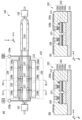
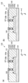
- 1A to 1C are diagrams illustrating the structure of an InP modulator 100 according to a first embodiment of the present disclosure, in which (a) is a top view, (b) is a cross-sectional view along the Ib-Ib cross-sectional line, and (c) is a cross-sectional view along the Ic-Ic cross-sectional line.
- 1A is a cross-sectional view in the width direction showing a configuration in which the heater mechanism 108 is arranged differently as another configuration of the InP modulator 100 according to the first embodiment of the present disclosure
- (a) is a cross-sectional view taken along the Ib-Ib cross-sectional line in FIG.
- (b) is a cross-sectional view taken along the Ic-Ic cross-sectional line in FIG. 1 when the InP optical waveguide 102 has a ridge structure
- (c) is a cross-sectional view taken along the Ib-Ib cross-sectional line in FIG. 1 when the InP optical waveguide 102 has a high mesa structure
- (d) is a cross-sectional view taken along the Ic-Ic cross-sectional line in FIG. 1 when the InP optical waveguide 102 has a high mesa structure.
- 1A and 1B are widthwise cross-sectional views showing another form of the InP modulator 100 according to the first embodiment of the present disclosure, where (a) shows a cross-sectional view taken along the Ib-Ib cross-sectional line in FIG. 1 , and (b) shows a cross-sectional view taken along the Ic-Ic cross-sectional line in FIG. 1 .
- 1A and 1B are widthwise cross-sectional views showing another form of the InP modulator 100 according to the first embodiment of the present disclosure, where (a) shows a cross-sectional view taken along the Ib-Ib cross-sectional line in FIG. 1 , and (b) shows a cross-sectional view taken along the Ic-Ic cross-sectional line in FIG. 1 .
- FIGS. 1A and 1B are cross-sectional views showing another embodiment of the InP modulator 100 according to the first embodiment of the present disclosure, in which (a) shows an embodiment in which the heater mechanism 108 is provided on the n-InP 102a, and (b) shows an embodiment in which one side of the heater mechanism 108 is disposed on the n-InP 102a and the other side is disposed on the substrate 110.
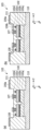
- 6A and 6B are longitudinal cross-sectional views illustrating the structure of an InP modulator 600 according to a second embodiment of the present disclosure, where (a) shows the structure without a carrier 603 and (b) shows the structure with a carrier 603.
- a single Mach-Zehnder modulator will be shown as an example below, but an IQ modulator or Twin-IQ modulator in which a plurality of such modulators are arranged may be used.
- an InP modulator will be described as an example below, but a semiconductor optical modulator made of other materials such as GaAs may be used.
- FIG. 1 illustrates the structure of an InP modulator 100 according to a first embodiment of the present disclosure, with (a) showing a top view, (b) showing a cross-sectional view along the Ib-Ib cross-sectional line, and (c) showing a cross-sectional view along the Ic-Ic cross-sectional line. As shown in FIG.
- the InP modulator 100 includes a 1-input, 2-output (1 ⁇ 2) multimode interference waveguide (MultiMode-Interferometer: hereinafter referred to as MMI) 101, an InP optical waveguide 102 through which light branched by the MMI 101 propagates, a phase modulation section 103 that performs phase modulation of the propagating light, a phase adjustment electrode 104 that is installed on the output side of the phase modulation section 103 and performs phase adjustment of the phase-modulated light, and a 2 ⁇ 1 MMI 105 that is installed on the output side of the phase adjustment electrode 104 and combines the branched light and outputs it to the outside.
- MMI multimode interference waveguide
- the InP modulator 100 is a Mach-Zehnder type optical modulator.
- the phase modulation unit 103 further includes a substrate 110, an optical waveguide 102 formed on the substrate 110, an RF phase modulation electrode 106 functioning as an electrode for the applied RF, an RF electrode 107 for applying the high frequency supplied from the RF phase modulation electrode 106 to the optical waveguide 102, a heater mechanism 108 for heating the optical waveguide 102, and a dielectric layer 111 formed on the substrate 110 and covering the periphery of the optical waveguide 102 and the heater mechanism 108.
- the heater mechanism 108 is connected to a metal wiring 112, which is integrated into one by PADs 109a and 109b and connected to an external power supply and GND. Note that, although FIG.
- the metal wiring 112 may be the same as the heater mechanism 108 or may be a completely different metal wiring. Also, in FIG. 1, the heater mechanism 108 is shown as being thicker and the metal wiring 112 as being thinner, but the heater mechanism 108 may be thinner and the metal wiring 112 may be thicker.
- the optical waveguide 102 has a nipn layer structure in which a first cladding layer 102a formed of at least one n-type semiconductor layer formed on a substrate, a second cladding layer 102b formed of at least one p-type semiconductor layer formed on 102a, a non-doped semiconductor core layer 102c formed on 102b, and a third cladding layer 102d formed of at least one n-type semiconductor layer formed on the semiconductor core layer 102c are stacked.
- the semiconductor core layer 102c includes a multi-quantum well (hereinafter referred to as MQW) layer using a material system such as non-doped InP, InGaAsP, or InGaAlAs.
- MQW multi-quantum well
- the band gap wavelength of the MQW layer is set arbitrarily within a range in which the electro-optic effect is effective and optical absorption is not a problem at the optical wavelength used.
- the semiconductor core layer 102c functions as a core through which light propagates.
- This nipn layer structure can reduce the thickness of the p layer, which has a large effect on high-frequency loss, and can also make the contact surface with the metal RF electrode 107 the n layer, making it possible to significantly reduce high-frequency loss compared to a conventional pin layer structure.
- the optical waveguide 102 may have a pin layer structure.
- the RF phase modulation electrode 106 has a capacitance-loaded structure, and includes a main line portion 106a and T-shaped portions 106b that branch off periodically from the main line portion 106a in order to apply a modulation signal to the InP optical waveguide 102.
- the InP modulator 100 is called a capacitance-loaded type because the T-shaped portions 106b are structured to add capacitance. Note that for simplification, only three T-shaped portions 106b are depicted in FIG. 1, but this is for illustrative purposes only, and three or more T-shaped portions 106b may be arranged, or even fewer. Also, in this embodiment, a capacitance-loaded structure is shown as an example, but this patent structure is also effective for structures other than capacitance-loaded structures.
- the heater mechanism 108 supplies heat (heats) to the MQW that constitutes the non-doped semiconductor core layer 102c of the InP modulator 100 and contributes to phase modulation.
- the mechanism can control the temperature of the MQW without using a Peltier element.
- the heater mechanism 108 By controlling the temperature of the MQW with the heater mechanism 108, it is possible to appropriately adjust the amount of refractive index effect based on the optical absorption and quantum confined Stark effect (QCSE) of the MQW. For example, when the temperature of the MQW increases, the band edge shifts to the long wavelength side, making it suitable for operation on the long wavelength side.
- the heater mechanism 108 can usually be metal.
- the heater mechanism 108 is placed directly under the thickness direction (z direction) of the main line portion 106a, it will affect the high-frequency electromagnetic field distribution of the RF phase modulation electrode 106 and the RF electrode 107, and as a result, the high-frequency characteristics of the InP modulator 100 may be deteriorated. Therefore, it is desirable that the heater mechanism 108 is arranged at a distance from the RF phase modulation electrode 106 and the RF electrode 107 such that it does not interfere with them (does not affect the electromagnetic field distribution of each high frequency) (for example, as shown in FIGS.
- the heater mechanism 108 since the heater mechanism 108 needs to heat all of the MQW layer that contributes to the phase modulation, it is desirable that the length in the x direction is equal to or longer than the length in the x direction of the RF phase modulation electrode 106.
- the resistance value of the heater mechanism 108 may be set arbitrarily depending on the design. For example, the resistance of the heater mechanism 108 may be set higher only in the peripheral region where the RF electrode 107 connected to the T-shaped portion 106b is installed than in other regions. However, since it is necessary for the optical modulator to have the desired amount of heat generation, it is desirable for the resistance value of the heater mechanism 108 to be at least 300 ⁇ or more.
- the heater mechanism 108 is configured so that each branched arm of the optical waveguide 102 can be uniformly heated. For this reason, the heater mechanism 108 is provided for each branched optical waveguide 102. Furthermore, in order to supply equal heat to each branched optical waveguide 102, it is desirable that the heater mechanism 108 is aggregated in one PAD 109a, b and connected to a power source (voltage source or current source) and GND. For example, if the InP modulator 100 is a Twin-IQ modulator or the like, it will have a configuration in which four Mach-Zehnder modulators are integrated, so eight heater mechanisms 108 are required.
- PAD109a, b When such a Twin-IQ modulator is used for HB-CDM, the number of required PADs and pins may increase, and control may become difficult. Therefore, it is desirable that all eight heater mechanisms 108 are aggregated in the same PAD 109a, b. Note that the shape of PAD109a, b is depicted as a circle in FIG. 1, but this is for illustrative purposes only and may be, for example, a square.
- the structure of the optical waveguide 102 is preferably a ridge structure from the viewpoint of directly heating the semiconductor core layer 102c.
- the structure may be a high mesa structure, but in such a case, the width (length in the y direction) of the optical waveguide 102 is processed to be the same width as the third cladding layer 102d, so the heater mechanism 108 cannot be installed on the semiconductor core layer 102c. Therefore, when the optical waveguide 102 has a high mesa structure, the heater mechanism 108 needs to be placed in another position (for example, on the substrate 110) as described later, and this reduces the heating efficiency of the semiconductor core layer P102c.
- the heater mechanism 108 can be placed on the semiconductor core layer 102c, so it is possible to directly heat the semiconductor core layer 102c. From this viewpoint, it can be said that the structure of the optical waveguide 102 is more effective as a ridge structure than a high mesa structure. However, even if the heater mechanism 108 is installed in another position (e.g., on the substrate 110), it is possible to heat the semiconductor core layer 102c, so the heater mechanism 108 does not necessarily have to be installed on the semiconductor core layer 102c.
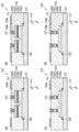
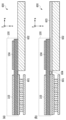
- FIG. 2 is a cross-sectional view in the width direction showing a different arrangement of the heater mechanism 108 as another embodiment of the InP modulator 100 according to the first embodiment of the present disclosure, where (a) is a cross-sectional view taken along the Ib-Ib cross-section line in FIG. 1 when the optical waveguide 102 has a ridge structure, (b) is a cross-sectional view taken along the Ic-Ic cross-section line in FIG. 1 when the optical waveguide 102 has a ridge structure, (c) is a cross-sectional view taken along the Ib-Ib cross-section line in FIG.
- the heater mechanism 108 may be disposed on the substrate 110.
- the structure of the optical waveguide 102 may be a ridge structure or a high mesa structure.
- the efficiency of heating the semiconductor core layer 102c including the MQW is reduced compared to the configuration shown in FIG. 1.
- this configuration has the advantage that the distance between the heater mechanism 108 and the RF phase modulation electrode 106 and the RF electrode 107 is greater than in the configuration shown in FIG. 1, and therefore degradation of the high frequency characteristics can be suppressed.
- the heater mechanism 108 when the heater mechanism 108 is close to the RF phase modulation electrode 106 and the RF electrode 107, the heater mechanism 108, which is usually made of metal, affects the high-frequency electromagnetic field distribution of the RF phase modulation electrode 106 and the RF electrode 107, and as a result, the high-frequency characteristics of the InP modulator 100 may deteriorate. From this perspective, in the InP modulator 100 according to the present disclosure, it is desirable to arrange the heater mechanism 108 and the RF phase modulation electrode 106 so that the distance between them is as long (separate) as possible. For example, in a form in which the heater mechanism 108 is installed on the substrate 110 as shown in FIG.
- the distance in the thickness direction (z direction) between the RF phase modulation electrode 106 and the RF electrode 107 and the heater mechanism 108 can be increased by making the dielectric layer 111 a thick film, etc.
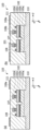
- a via 301 may be installed between the T-shaped portion 106b and the RF electrode 107 as shown in FIG. 3.
- the RF electrode 107 may be made thick to increase the distance in the thickness direction between the RF phase modulation electrode 106 and the heater mechanism 108. With such a configuration, it is possible to eliminate the need for the via 301.
- FIG. 1 As another example, as shown in FIG.
- a structure may be used in which only the region of the dielectric layer 111 corresponding to the upper part of the optical waveguide 102 is thinned (in other words, the dielectric layer 111 is thickened only in the region where the main line portion 106a is arranged).
- the distance between the T-shaped portion 106b and the heater mechanism 108 may be partially shortened.
- the deterioration of the high frequency characteristics as described above may be suppressed by controlling the arrangement or dimensions of the heater mechanism 108.
- the diameter plane perpendicular to the xy plane
- the influence of the heater mechanism 108 on the high frequency electromagnetic field distribution of the RF phase modulation electrode 106 can be suppressed.
- the width (length in the y direction) of the heater mechanism 108 is 1 ⁇ m or less, and if it can be made 0.1 ⁇ m or less, the influence on the high frequency characteristics can be almost negligible.
- the diameter is extremely narrow, there is a concern that the wire may break when heated, so it is necessary to ensure a diameter dimension that does not cause this break.
- the distance between the main line portion 106a and the heater mechanism 108 in the thickness direction (z direction) and width direction (y direction) is at least 5 ⁇ m or more.
- the diameter of the heater mechanism 108 is, for example, 1 ⁇ m or less in both thickness and width.
- the heater mechanism 108 it is desirable for the heater mechanism 108 to have a heat generation amount of at least about 100°C, from the viewpoint that it is necessary to realize heat generation of at least about 40 to 60°C, the temperature of which is controlled by a Peltier element in a typical InP modulator. Therefore, for example, it is desirable for the heater mechanism 108 to be configured to have a resistance value of at least 300 ⁇ or more.
- the third cladding layer 102b may be set to have a higher thermal resistance than the semiconductor cladding layer 102c in order to suppress the release of heat to the lower part of the semiconductor core layer 102c.
- the heater mechanism 108 may also be disposed on the first cladding layer 102a as shown in FIG. 5. Furthermore, the heater mechanisms 108 may each be disposed at a different location, for example, one on the first cladding layer 102a and the other on the substrate 110.
- the operating wavelength range of the InP modulator can be expanded by controlling the amount of heat generated by the heater mechanism 108 with either current or voltage depending on the operating wavelength.
- InP modulators generally use a refractive index effect caused by changes in band edge absorption called QCSE.
- Optical semiconductors generally have the characteristic that their optical absorption is large on the short wavelength side and small on the long wavelength side.
- the modulation efficiency decreases on the long wavelength side, and it was necessary to change the PL wavelength of the MQW layer separately for modulators operating in the C band and modulators operating in the L band (for example, in InP modulators using conventional technology, the PL wavelength had to be longer in the L band than in the C band).
- the InP modulator 100 for example, at the same temperature, the amount of heat generated by the heater mechanism 108 is increased during operation on the long wavelength side, increasing the temperature of the MQW and shifting the band edge to the long wavelength side, while the amount of heat generated on the short wavelength side is reduced, and the amount of shift of the band edge to the long wavelength side is reduced by lowering the temperature of the MQW.
- the temperature of the semiconductor core layer having the MQW layer can be controlled by the heater mechanism 108.
- it is also possible to use both this structure and a Peltier element (details will be described in the second embodiment below).
- the driver IC has a temperature monitor mechanism
- MQW i-InP 102c
- control is possible such that the heater mechanism 108 heats up to the desired temperature using that temperature as the monitor value. For example, when operating at the same wavelength, control is possible such that when the driver monitor temperature is high, heating of the heater mechanism 108 is suppressed, and when the monitor temperature is low, heating of the heater is promoted.
- the InP modulator 100 When the InP modulator 100 according to the present embodiment described above is used in HB-CDM, it is desirable to set the operating temperature range of the phase modulation section 103 to a range different from that of semiconductor optical modulators according to conventional technology.
- HB-CDM is required to operate at least at an ambient temperature of -5 to 75°C.
- the heater mechanism 108 can only heat, not cool. Therefore, for example, for any one wavelength, the temperature of the semiconductor core layer 102c (MQW) needs to be controlled to a constant temperature by the heater mechanism 108 within the ambient temperature range of -5 to 75°C. Therefore, specifically, the operating temperature of the InP modulator 100 needs to be controlled by the heater mechanism 108 to be equal to or higher than the ambient temperature of 75°C.
- the temperature is controlled by a Peltier element in the range of approximately 40 to 60°C.
- the appropriate operating temperature of the InP modulator 100 according to this embodiment is set to 40 to 60°C as in the conventional technology, when the environmental temperature reaches 75°C, cooling cannot be performed, and the desired temperature cannot be achieved. Therefore, in order to maintain the temperature of the semiconductor core layer 102c (MQW) within the appropriate range at an environmental temperature of -5 to 75°C for operation of any one wavelength, at least the InP modulator 100 according to this embodiment must be designed to operate properly at 75°C or higher. In addition, taking into consideration power consumption and stable operation of the heater mechanism 108, it is desirable to set the appropriate temperature to within about the maximum environmental temperature +10°C.
- This embodiment relates to an InP modulation device including the InP modulator 100 described in the first embodiment and a Peltier element.
- FIG. 6A and 6B are longitudinal cross-sectional views illustrating the structure of an InP modulation device 600 according to a second embodiment of the present disclosure, where (a) shows a structure without a carrier 603 and (b) shows a structure including a carrier 603.
- the InP modulation device 600 according to this embodiment has a structure in which the InP modulator 100 according to the first embodiment is mounted on a Peltier element 601 and a dielectric substrate 602.
- the InP modulation device 600 may further include a carrier 603 above the Peltier element 601 and the dielectric substrate 602 and below the InP modulator 100.
- the Peltier element 601 In order to apply heat most efficiently (to suppress the power consumption of the Peltier element as much as possible), it is desirable to install the Peltier element 601 so that only the phase modulation unit 103 is placed on the Peltier element 601, as shown in FIG. 6. For further optimization, it is optimal to provide the Peltier element only on the lower part of the phase modulation arm. However, this is just one example, and the entire chip may be mounted on the Peltier element 601. In that case, compared to a normal modulator, the provision of an extra heater mechanism results in an increase in power consumption. This is because the power consumption of the Peltier depends on the area of the Peltier. Therefore, considering the increase in power consumption of the Peltier element due to heat generation by the heater mechanism, in an optical modulator with this heater mechanism, the size of the Peltier element needs to be very small in order to achieve the same power consumption as before.
- the dielectric substrate 602 does not necessarily have to be included in the InP modulation device 600, but it is desirable to have one installed from the viewpoint of securing an area for mounting optical mounting members (not shown) such as lenses.
- the dielectric substrate 602 may be made of ceramics such as aluminum nitride (AlN) or metals, which have excellent heat dissipation properties.
- the carrier 603 preferably further includes a thermal isolation groove 604 from the viewpoint of thermal isolation between the RF phase modulation electrode 106 and the phase adjustment electrode 104.
- the phase adjustment electrode 104 is generally configured as a heater, and in that case, heat from the heater of the phase adjustment electrode 104 flows into the Peltier element 601, increasing the power consumption of the Peltier element 601.
- the carrier 603 may be in a form that overhangs the Peltier element 601, or may be configured such that an additional component (e.g., a dielectric substrate 602) is installed below the carrier 603.
- the carrier 603 may have a step (not shown) only in the area where an optical mounting member such as a lens is mounted, as necessary.
- the InP modulation device 600 having such a configuration includes a Peltier element 601, and by controlling the temperature of the Peltier element 601 according to the wavelength, it is possible to widen the operating wavelength range, similar to the effect of the heater mechanism 108 of the InP modulator 100.
- the Peltier element 601 is placed only in the area corresponding to the RF phase modulation electrode 106. Therefore, compared to the case where the entire InP modulation device 600 is placed on the Peltier element, the area occupied by the Peltier element 601 can be reduced, making it possible to suppress power consumption.
- the temperature of the Peltier element is not switched for each wavelength, so it is highly likely that the above-mentioned operation would be difficult.
- the Peltier element is operated with a constant set temperature, in which case the heater mechanism 108, which has a configuration similar to that of the first embodiment, can be used to pinpoint the amount of heat controlled for each operating wavelength and applied only to the relevant part, thereby expanding the operating wavelength and achieving C+L band operation, etc.
- the heater mechanism 108 which has a configuration similar to that of the first embodiment, can be used to pinpoint the amount of heat controlled for each operating wavelength and applied only to the relevant part, thereby expanding the operating wavelength and achieving C+L band operation, etc.
- the Peltier element 601 can switch the temperature for each wavelength, it is also possible to expand the operating wavelength without using the heater mechanism 108.
- the semiconductor optical modulator (InP modulator) according to the present disclosure is capable of expanding the wavelength operating range compared to conventional technologies.
Landscapes
- Physics & Mathematics (AREA)
- Nonlinear Science (AREA)
- General Physics & Mathematics (AREA)
- Optics & Photonics (AREA)
- Optical Modulation, Optical Deflection, Nonlinear Optics, Optical Demodulation, Optical Logic Elements (AREA)
Abstract
従来技術による半導体光変調器より広い動作波長帯域にも対応可能である半導体光変調器を提供する。本開示による半導体光変調器は、半導体基板上に、少なくとも1層以上のn型半導体またはp型半導体で形成された下部クラッド層と、MQW層を含むノンドープの半導体で形成されたコア層と、少なくとも1層以上のn型半導体またはp型半導体で形成された上部クラッド層が順に積層された構造を有する光導波路と、光導波路を伝搬する光の位相変調を行う位相変調部と、を備え、位相変調部は、光導波路を加熱するヒーター機構と、光導波路に接続されるRF電極と、を備え、光導波路はリッジ構造を有し、ヒーター機構は、光導波路のコア層上に形成されていることを特徴とする。
Description
本開示は、半導体光変調器に関する。
近年における光ファイバ通信システムでは、デジタルコヒーレントをはじめとしたデジタル信号処理技術の導入により、1波長当たり100Gbpsの基幹網伝送技術が確立されている。現在では、この基幹網伝送技術は、1波長当たり400-600Gbpsまで高速化が進んでおり、実用化のレベルに達しつつある。
400Gbpsを超える通信システムでは、アナログ部品の広帯域化(例えば、変調帯域40GHz以上)が求められることから、高周波(Radio Frequency:以下、RFともいう)の損失低減及び小型化を目的として、送信側ではRFドライバ(ドライバIC)と光変調器が一体パッケージ実装された形態が注目されている。このような実装形態を用いた送信器は、High-Bandwidth Coherent Driver Modulator(HB-CDM:高速ドライバ集積光変調器)という名前でOIF(The Optical Internetworking Forum)において標準化されている(例えば、非特許文献1参照)。また、HB-CDMにおいては、インジウムリン(InP)変調器が主に使用されている(例えば、非特許文献2参照)。
光送信デバイスにおいて、近年では、従来のニオブ酸リチウム(LN)光変調器に代わり、半導体ベースの光変調器がデバイスの小型化及び低コスト化の観点で注目を集めている。特に、より高速な変調動作に対しては、InPに代表される化合物半導体が主に用いられ、また、より小型化及び低コスト化が重要視されるシステムにおいては、シリコン(Si)ベースの光デバイスに研究開発が集中している。
半導体光変調器においても材料固有の得失があり、例えば、InP変調器は高速な変調動作に優れる反面、バンド端吸収効果を制御するために、変調動作時には光変調器チップの温度制御が必須と考えられている。一方、LN変調器やSi変調器は、温度制御が不要となるメリットがあり、低消費電力化に有利であると考えられている。
InP変調器をモジュール化する場合、温度制御のために、光変調器チップはペルチェ素子上に実装されることが必要となり、これが消費電力の増加の一因となり得る。加えて、当該ペルチェ素子の配置によりパッケージサイズを小型化できないという課題もある。したがって、ペルチェ素子を不要とする、或いはペルチェ素子を配置する領域を縮小することができれば、高速な変調動作に優れるInP変調器を搭載した高速で低消費電力かつ低背の光モジュールを実現することが可能である。
また、InP変調器はバンド端吸収効果を用いるため、C帯用とL帯用でエピ構造の変更(PL波長等による吸収のコントロール)を行うことが必須であり、C帯とL帯でチップを共用することが困難であるという課題もある。
Implementation Agreement for the High Bandwidth Coherent Driver Modulator (HB-CDM) , OIF-HB-CDM-02.0 (2021)https://www.oiforum.com/wp-content/uploads/OIF-HB-CDM-02.0.pdf
J. Ozaki, Y. Ogiso, Y. Hashizume, H. Yamazaki, K. Nagashima and M. Ishikawa, "Coherent Driver Modulator With Flexible Printed Circuit RF Interface for 128-Gbaud Operations", IEEE Photonics Technology Letters, vol. 34, no. 23, pp. 1289-1292 (2022) doi: 10.1109/LPT.2022.3212678.
本開示は、上記のような課題に対して鑑みてなされたものであり、その目的とするところは、従来技術による半導体光変調器より広い動作波長帯域(例えば、C+L帯)にも対応可能な半導体光変調器を提供することにある。
上記のような課題に対し、本開示では、半導体光変調器であって、半導体基板上に、少なくとも1層以上のn型半導体またはp型半導体で形成された下部クラッド層と、MQW層を含むノンドープの半導体で形成されたコア層と、少なくとも1層以上のn型半導体またはp型半導体で形成された上部クラッド層が順に積層された構造を有する光導波路と、光導波路を伝搬する光の位相変調を行う位相変調部と、を備え、位相変調部は、光導波路を加熱するヒーター機構と、光導波路に接続されるRF電極と、を備え、光導波路はリッジ構造を有し、ヒーター機構は、光導波路のコア層上に形成されていることを特徴とする、半導体光変調器を提供する。
以下に、図面を参照しながら本開示の種々の実施形態について詳細に説明する。同一又は類似の参照符号は同一又は類似の要素を示し重複する説明を省略する場合がある。材料及び数値は例示を目的としており本開示の技術的範囲の限定を意図していない。以下の説明は、一例であって本開示の一実施形態の要旨を逸脱しない限り、一部の構成を省略若しくは変形し、又は追加の構成とともに実施することができる。
(第1の実施形態)
以下に、本開示の第1の実施形態について、図面を参照して詳細に説明する。以下では一例として、単体のマッハツェンダー変調器を示すが、これを複数配列した、IQ変調器やTwin-IQ変調器等であってもよい。また、以下では、一例として、InP変調器を例に挙げて説明をしているが、GaAs等の他の材料系の半導体光変調器であってもよい。
以下に、本開示の第1の実施形態について、図面を参照して詳細に説明する。以下では一例として、単体のマッハツェンダー変調器を示すが、これを複数配列した、IQ変調器やTwin-IQ変調器等であってもよい。また、以下では、一例として、InP変調器を例に挙げて説明をしているが、GaAs等の他の材料系の半導体光変調器であってもよい。
図1は、本開示の第1の実施形態による、InP変調器100の構造を例示する図であり、(a)は上面図を、(b)はIb-Ib断面線における断面図を、(c)はIc-Ic断面線における断面図を、それぞれ示している。図1に示される通り、InP変調器100は、1入力2出力(1×2)の多モード干渉型導波路(MultiMode-Interferometer:以下、MMIという)101と、MMI101で分岐された光が伝搬するInP光導波路102と、伝搬する光の位相変調を行う位相変調部103と、位相変調部103の出力側に設置され、位相変調された光の位相調整を行う、位相調整電極104と、位相調整電極104の出力側に設置され、分岐された光を合波して外部に出力する2×1MMI105と、を含む。図1に示されるように、InP変調器100は、マッハツェンダー型の光変調器である。
図1(a)及び(b)に示される通り、位相変調部103は、基板110と、基板110上に形成された光導波路102と、印加されるRFの電極として機能するRF位相変調電極106と、RF位相変調電極106から供給された高周波を光導波路102に印加するための電極であるRF電極107と、光導波路102を加熱するヒーター機構108と、基板110上に形成され、光導波路102及びヒーター機構108の周囲を覆う誘電体層111と、をさらに含む。ヒーター機構108は金属配線112と接続され、当該金属配線112は、PAD109a、bで1つに集約され、外部の電源及びGNDと接続される。なお、図1では、金属配線112を含む形態を図示しているが、当該金属配線112の部分もヒーター機構108と同等な金属配線としてもよく、全く別の金属配線としてもよい。また、図1では、ヒーター機構108の方が太く、金属配線112の方が細くなるように図示されているが、ヒーター機構108の方が細く、金属配線112の方が太い形態であってもよい。
光導波路102は、基板上に形成された少なくとも1層以上のn型半導体層で形成された第1のクラッド層102aと、102aに形成された少なくとも1層以上のp型半導体層で形成された第2のクラッド層102bと、102b上に形成されたノンドープの半導体コア層102cと、当該半導体コア層102cに形成された少なくとも1層以上のn型半導体層で形成された第3のクラッド層102dが積層された、nipn層構造を有する。半導体コア層102cは、例えば、ノンドープのInP、InGaAsP、InGaAlAsなどの材料系が用いられた多量子井戸(Multi Quantum Well:以下、MQWという)層を含む。当該MQW層のバンドギャップ波長は、使用する光波長において、電気光学効果が有効に作用し、且つ、光吸収が問題とならないような範囲に任意で設定される。ここで、半導体コア層102cは、光が伝搬するコアとして機能する。このようなnipn層構造は、高周波損失への影響が大きいp層を薄くし、且つ金属であるRF電極107とのコンタクト面をn層とすることができるため、従来のpin層構造に比べ、高周波損失を大幅に低減することが可能である。但し、これは例示を目的としており、光導波路102は、pin層構造を有していてもよい。
RF位相変調電極106は容量装荷構造を有しており、主線路部106aと、InP光導波路102に変調信号を印加するために、主線路部106aから周期的に分岐したT字部106bと、を含む。InP変調器100は、当該T字部106bが容量を追加する構造であるため、容量装荷型と呼ばれている。尚、図1では簡略化のため、T字部106bは3体のみの描画としているが、これは例示を目的としており、3体以上のT字部106bが配置されてよく、それ以下であってもよい。また、本実施例では、一例として容量装荷構造を示しているが、本特許構造は容量装荷構造以外にも有効である。
ヒーター機構108は、InP変調器100のノンドープ半導体コア層102cを構成する、位相変調に寄与するMQWに熱を供給(加熱)する。このような構成により、ペルチェ素子を用いずとも、MQWの温度制御が可能な機構とすることができる。MQWの温度をヒーター機構108で制御することで、当該MQWの光吸収及び量子閉じ込めシュタルク効果(Quantum Confined Stark Effect:QCSE)に基づく屈折率効果の量を適切に調整することが可能である。例えば、MQWの温度が上がるとバンド端が長波側にシフトするため、より長波長側での動作に適した状態となる。ヒーター機構108は、通常、金属であり得る。そのため、主線路部106aの厚さ方向(z方向)の直下にヒーター機構108が配置されると、RF位相変調電極106及びRF電極107の高周波の電磁界分布に影響を与え、結果としてInP変調器100の高周波特性が劣化し得る。したがって、ヒーター機構108は、RF位相変調電極106及びRF電極107から、干渉しない(各々の高周波の電磁界分布に影響を及ぼさない)程度の距離を設けて(例えば、図1(a)、(b)に示されるように、幅方向(y方向)に対して主線路部106aとRF電極107の間に位置するように)、且つRF位相変調電極106及びRF電極107の長手方向(x方向)に対して平行になるように配置されることが望ましい。また、ヒーター機構108は、位相変調に寄与する部分のMQW層を全て加熱する必要があるため、x方向の長さは、RF位相変調電極106のx方向の長さと同等又はそれ以上であることが望ましい。ヒーター機構108の抵抗値は、設計に応じて任意に設定されてよい。例えば、T字部106bに接続されたRF電極107が設置される周辺領域のみ、ヒーター機構108の抵抗を他の領域に比べて高く設定されてもよい。但し、光変調器として所望の発熱量を有することが必要であることから、ヒーター機構108の抵抗値は、少なくとも300Ω以上であることが望ましい。
ヒーター機構108は、光導波路102の分岐した各々のアームに対し、均一に加熱できるように構成されることが望ましい。このため、ヒーター機構108は、分岐した光導波路102の各々に対して設けられる。さらに、ヒーター機構108は、分岐した光導波路102各々に対し、同等な熱を供給するために、1つのPAD109a、bに集約された上で電源(電圧源又は電流源)及びGNDと接続されることが望ましい。例えば、InP変調器100が、Twin-IQ変調器等である場合には、マッハツェンダー変調器が4つ集積された構成となるため、8本のヒーター機構108が必要となる。このようなTwin-IQ変調器をHB-CDMに用いる場合、必要なPADやピンの数が増大し得るととともに、制御も困難となり得る。したがって、8本すべてのヒーター機構108が同一のPAD109a、bに集約されることが望ましい。尚、PAD109a、bの形状は、図1では、丸形状として描画されているが、これ例示を目的としており、例えば、正方形であってもよい。
位相変調部103において、光導波路102の構造は、半導体コア層102cを直接的に加熱するという観点から、リッジ構造であることが望ましい。当該構造は、ハイメサ構造であってもよいが、そのような場合、光導波路102の幅(y方向の長さ)は、第3のクラッド層102dと同じ幅で加工されることとなるため、半導体コア層102c上にヒーター機構108を設置することができなくなる。したがって、光導波路102がハイメサ構造を有する場合では、ヒーター機構108は、後述するように他の位置(例えば、基板110上)に配置される必要があり、これに伴って、半導体コア層P102cの加熱効率が低下する。一方、光導波路102の構造がリッジ構造である場合、ヒーター機構108は、半導体コア層102c上に設置されることができるため、半導体コア層102cを直接的に加熱することが可能となる。このような観点から、光導波路102の構造は、ハイメサ構造よりリッジ構造である方が有効と言える。但し、ヒーター機構108が、他の位置(例えば、基板110上)に設置されたとしても、半導体コア層102cを加熱すること自体は可能であるため、ヒーター機構108は、必ずしも半導体コア層102c上に設置されなくともよい。
図2は、本開示の第1の実施形態によるInP変調器100の別の形態として、ヒーター機構108の配置が異なる形態を示す幅方向の断面図であり、(a)は、光導波路102がリッジ構造である場合の、図1におけるIb-Ib断面線における断面図を、(b)は、光導波路102がリッジ構造である場合の、図1におけるIc-Ic断面線における断面図を、(c)は、光導波路102がハイメサ構造である場合の、図1におけるIb-Ib断面線における断面図を、(d)は、光導波路102がハイメサ構造である場合の、図1におけるIc-Ic断面線における断面図を、それぞれ示している。図2に示される通り、InP変調器100では、ヒーター機構108は、基板110上に配置されてもよい。このような形態とすれば、光導波路102の構造は、リッジ構造であってもよく、ハイメサ構造であってもよい。上述の通り、ヒーター機構108を基板110上に配置した形態では、図1に示される形態に比べ、MQWを含む半導体コア層102cの加熱という観点では効率が低下する。しかしながら、このような形態は、ヒーター機構108と、RF位相変調電極106及びRF電極107との距離が、図1に示される形態に比べて大きくなるため、高周波特性への劣化を抑制できるという特徴を有する。
上述した様に、ヒーター機構108と、RF位相変調電極106及びRF電極107との距離が近い場合、通常、金属であるヒーター機構108がRF位相変調電極106及びRF電極107の高周波の電磁界分布に影響を与え、結果としてInP変調器100の高周波特性が劣化し得る。このような観点から、本開示によるInP変調器100では、ヒーター機構108とRF位相変調電極106の配置は、可能な限り各々の距離が長くなる(離れる)ように配置することが望ましい。例えば、図2に示されるような、ヒーター機構108が基板110上に設置される形態では、誘電体層111を厚膜とすること等により、RF位相変調電極106及びRF電極107とヒーター機構108との厚さ方向(z方向)の距離を長くすることができる。別の例として、図3に示されるように、T字部106bとRF電極107との間にビア301を設置してもよい。また、図3のようにRF電極107が誘電体層111に埋め込まれている場合には、当該RF電極107を厚膜とすることで、RF位相変調電極106とヒーター機構108との厚さ方向の距離を長くするような構成としてもよい。このような構成とすれば、ビア301を不要とすることも可能である。またさらに別の例として、図4に示されるように、誘電体層111における光導波路102の上部に相当する領域のみを薄化する(換言すれば、主線路部106aが配置される領域のみ、誘電体層111を厚くする)構造としてもよい。但し、図4に示されるような形態の場合、T字部106bとヒーター機構108との間の距離は、部分的に短くなり得る。
また、ヒーター機構108の配置又は寸法の制御によって、上述したような高周波特性劣化の抑制が行われてもよい。例えば、ヒーター機構108の径(xy面に垂直な面)を細くすることにより、ヒーター機構108がRF位相変調電極106の高周波の電磁界分布に与える影響を抑制することができる。ヒーター機構108の幅(y方向の長さ)は、1μm以下とすることが望ましく、仮に0.1μm以下とすることができれば、高周波特性への影響はほとんど無視することができる。但し、当該径が極度に細くなる場合、加熱時の断線が懸念されるため、この断線が生じないような径の寸法は確保される必要がある。また、主線路部106aとヒーター機構108との厚さ方向(z方向)及び幅方向(y方向)の距離は、少なくとも5μm以上であることが望ましい。このような観点を考慮すると、ヒーター機構108の径は、例えば、厚さ及び幅が共に1μm以下であることが望ましい。
一方で、ヒーター機構108は、通常のInP変調器がペルチェ素子で温度制御される40~60℃程度の発熱以上を実現する必要があるという観点から、少なくとも100℃程度の発熱量を有することが望ましい。したがって、例えば、ヒーター機構108は、少なくとも300Ω以上の抵抗値を有するように構成されることが望ましい。追加の例として、半導体コア層102cに温度を効率的に供給するという観点から、熱が半導体コア層102cの下部に放出されるのを抑制するために、第3のクラッド層102bは、熱抵抗を半導体クラッド層102cよりも高くなるように設定されてもよい。
また、ヒーター機構108は、図5に示される通り、第1のクラッド層102a上に設置されてもよい。さらに、ヒーター機構108は、例えば、一方は第1のクラッド層102a上、もう一方は基板110上というように、各々が別の位置に設置されてもよい。
このように構成される、本実施形態によるInP変調器100では、動作波長に応じて、ヒーター機構108の発熱量を電流又は電圧のいずれかにより制御すれば、InP変調器の動作波長範囲を広げることが可能となる。一般的に、InP変調器では、QCSEと呼ばれるバンド端吸収の変化による屈折率効果を用いる。一般的に光半導体の光吸収量は、短波側が大きく、長波側は小さいという特徴がある。そのため、幅広い波長帯で使用すると、長波側では変調効率が低くなるという事象が発生し、C帯動作用の変調器と、L帯動作用の変調器では、別途MQW層のPL波長を変更する必要があった(例えば、従来技術によるInP変調器では、C帯に比べてL帯はPL波長をより長波側にする必要があった)。これに対し、本実施形態によるInP変調器100では、例えば、同一温度下であれば、長波側の動作時によりヒーター機構108の発熱量を大きくすることで、MQWの温度を高めバンド端を長波側にシフトさせ、短波側では発熱量を小さくし、MQWの温度を下げることで、バンド端の長波側へのシフト量を小さくするというように、バンド端の変化量を波長に応じて調整することによって、これまでなかったC帯及びL帯で動作が可能なInP変調器とすることが可能となる。尚、後述するが、同様に、ペルチェ素子上にInP変調器が搭載されている場合には、ペルチェ素子の温度を波長に応じて変化させることでも同様の効果を得ることは可能である。
また、本実施形態によるInP変調器100では、MQW層を有する半導体コア層の温度をヒーター機構108により制御することが可能である。このため、従来技術におけるペルチェ素子を不要とすることが可能であり、本実施形態によるInP変調器100を用いた光モジュールの小型化・低消費電力化を実現することが可能となる。一方で,本構造を持ちつつペルチェ素子も使用するという併用も可能である(詳細は、後述の第2の実施形態にて述べる)。
さらに、HB-CDMのように、ドライバが、変調器のヒーター機構からの熱の影響を受ける程度に隣接して実装されるような形態において、ドライバICが温度モニタ機構を有する場合、ドライバICの温度モニタ機構を利用することにより、i-InP102c(MQW)温度の相対値を算出することが可能であるため、当該温度をモニタ値として、所望の温度になるようにヒーター機構108で加熱するというような制御が可能となる。例えば、同一波長で動作する場合、ドライバのモニタ温度が高い場合にはヒーター機構108の加熱を抑制し、モニタ温度が低い場合にはヒーターの加熱を促進するという制御が可能となる。
尚、上述した、本実施形態によるInP変調器100をHB-CDMに用いる場合、位相変調部103の動作温度の範囲は、従来技術による半導体光変調器とは異なる範囲で設定されることが望ましい。通常、HB-CDMでは、少なくとも環境温度が-5~75℃で動作することが求められる。一方、ヒーター機構108は、加熱しか行えず、冷却は行えない。そのため、例えば任意の1波長に関して考えると、半導体コア層102c(MQW)の温度は、-5~75℃の環境温度の範囲下において、ヒーター機構108によって温度は一定に制御される必要がある。そのため、具体的には、InP変調器100の動作温度は、ヒーター機構108により環境温度の75℃以上に制御される必要がある。従来技術による半導体光変調器では、およそ40~60℃の範囲で、ペルチェ素子により温度制御されるが、本実施形態によるInP変調器100の適正な動作温度を従来技術と同様に40~60℃で設定すると、環境温度が75℃になった際に、冷却を行うことができず、所望の温度を実現できないとう問題が生じる。そのため、任意の1波長の動作において、-5~75℃での環境温度下で半導体コア層102c(MQW)の温度を適正範囲に維持するためには、少なくとも本実施形態によるInP変調器100は、75℃以上で適正な動作が可能な設計となっている必要がある。尚、消費電力やヒーター機構108の安定動作も考慮し、最高環境温度+10℃以内程度に適正温度を納めるように設定するのが望ましい。
(第2の実施形態)
以下に、本開示の第2の実施形態について、図面を参照して詳細に説明する。本実施形態は、第1の実施形態で述べたInP変調器100とペルチェ素子を含むInP変調装置に関する。
以下に、本開示の第2の実施形態について、図面を参照して詳細に説明する。本実施形態は、第1の実施形態で述べたInP変調器100とペルチェ素子を含むInP変調装置に関する。
図6は、本開示の第2の実施形態による、InP変調装置600の構造を例示する長手方向の断面図であり、(a)はキャリア603を含まない構造を、(b)はキャリア603を含む構造を、それぞれ示している。図6に示される通り、本実施形態によるInP変調装置600は、第1の実施形態によるInP変調器100が、ペルチェ素子601及び誘電体基板602上に載置された構造を有する。また、図6(b)に示される通り、InP変調装置600は、ペルチェ素子601及び誘電体基板602の上、且つInP変調器100の下に、キャリア603をさらに含んでもよい。
ペルチェ素子601は、最も効率的な熱印加とする(可能な限りペルチェ素子の消費電力を抑圧する)ためには、図6に示される通り、位相変調部103のみが当該ペルチェ素子601上に載置されるように設置されることが望ましい。より最適化すると、位相変調アーム下部のみにペルチェ素子を設けることが最適である。ただし、本例は一例であり、チップ全体がペルチェ素子601上に搭載されていてもよい。その場合は通常の変調器に比べ、ヒーター機構を余分に設けていることで、消費電力が結果として増大してしまうことになる。これはペルチェの消費電力はペルチェの面積に依存するためである。そのため、ヒーター機構による発熱によるペルチェ素子の消費電力の増大を考慮すると、本ヒーター機構を有した光変調器において、従来通りの消費電力を実現するためにはペルチェ素子のサイズを非常に小さくする必要がある。
誘電体基板602は、必ずしもInP変調装置600に含まれる必要はないが、レンズ等の光学実装部材(図示せず)を搭載する領域を確保するという観点から、設置されることが望ましい。誘電体基板602には、放熱性に優れた窒化アルミニウム(AlN)等のセラミックスや金属が用いられ得る。
キャリア603は、RF位相変調電極106と位相調整電極104との間を熱分離するという観点から、熱分離溝604をさらに含むことが望ましい。これは、例えば位相調整電極104はヒーターで構成されるのがInP変調器では一般的であり、その場合、当該位相調整電極104のヒーターの熱が、ペルチェ素子601に流入し、当該ペルチェ素子601の消費電力が増えることになってしまうためである。また、キャリア603は、ペルチェ素子601からオーバーハングする形態であってもよく、当該キャリア603の下部に追加の構成要素(例えば、誘電体基板602)を設置するような構成としてもよい。加えて、キャリア603は、必要に応じて、レンズ等の光学実装部材が実装される領域にのみ、段差(図示せず)を有してもよい。
このような構成を有する、InP変調装置600は、ペルチェ素子601を含むため、当該ペルチェ素子601の温度を波長に応じて制御することにより、InP変調器100のヒーター機構108の効果と同様に、動作波長域を広げることが可能となる。本実施形態によるInP変調装置600では、ペルチェ素子601は、RF位相変調電極106に相当する領域のみに設置される。このため、InP変調装置600全体をペルチェ素子上に載置する場合に比べ、当該ペルチェ素子601が占有する領域を縮小することができ、消費電力の抑制が可能となる。
一方で、従来のInP変調器では、ペルチェ素子の温度を波長毎に切り替えることはなかったため、上記のような運用は難しい可能性が高い。この場合、ペルチェ素子の設定温度が一定として動作をさせるようなケースとなるが、その場合には、第1の実施形態と同様な構成であるヒーター機構108により、動作波長毎にコントロールした熱量を当該部分にのみピンポイントに印加することで動作波長を拡大し、C+L帯動作等を実現することが可能である。ただし、ペルチェ素子601が温度を波長毎に切り替えることができる場合は、ヒーター機構108を用いずとも動作波長の拡大を実現することも可能である。
以上述べた通り、本開示による半導体光変調器(InP変調器)は、波長動作範囲を従来技術に比べて拡大することが可能である。このような半導体光変調器は、従来技術より広帯域に適用できるような光変調器として、HB-CDM等の光ファイバ通信システム用デバイスへの適用が見込まれる。
Claims (8)
- 半導体光変調器であって、
半導体基板上に、少なくとも1層以上のn型半導体またはp型半導体で形成された下部クラッド層と、MQW層を含むノンドープの半導体で形成されたコア層と、少なくとも1層以上のn型半導体またはp型半導体で形成された上部クラッド層が順に積層された構造を有する光導波路と、
前記光導波路を伝搬する光の位相変調を行う位相変調部と、
を備え、
前記位相変調部は、
前記光導波路を加熱するヒーター機構と、
前記光導波路に接続されるRF電極と、
を備え、
前記光導波路はリッジ構造を有し、
前記ヒーター機構は、前記光導波路のコア層上に形成されていることを特徴とする、
半導体光変調器。 - 半導体光変調器であって、
半導体基板上に、少なくとも1層以上のn型半導体またはp型半導体で形成された下部クラッド層と、MQW層を含むノンドープの半導体で形成されたコア層と、少なくとも1層以上のn型半導体またはp型半導体で形成された上部クラッド層が順に積層された構造を有する光導波路と、
前記光導波路を伝搬する光の位相変調を行う位相変調部と、
を備え、
前記位相変調部は、
前記光導波路を加熱するヒーター機構と、
前記光導波路に接続されるRF電極と、
を備え、
前記光導波路はリッジ構造又はハイメサ構造を有し、
前記ヒーター機構は、前記基板上に形成されることを特徴とする、
半導体光変調器。 - 前記ヒーター機構は、前記RF電極の長手方向に対して平行になるように配置されており、抵抗値は300Ω以上である、請求項1または2に記載の半導体光変調器。
- 主線路部及び前記主線路部と前記RF電極とを接続する複数のT字部を含むRF位相変調電極をさらに備え、前記主線路部と前記ヒーター機構との厚さ方向及び幅方向の各々の距離は、少なくとも5μm以上であることを特徴とする、請求項3に記載の半導体光変調器。
- 前記光導波路は、半絶縁性基板上に形成されており、
前記基板上に形成された少なくとも1層以上n型半導体で構成される第一のn型半導体層と、
前記n型半導体層上に形成された少なくとも1層以上のp型半導体で構成されるp型半導体層と、
前記p型半導体層上に形成され、MQW層を含むノンドープの半導体で形成されたコア層と、
前記コア層上に形成された少なくとも1層以上のn型半導体で構成される第2のn型半導体層と、
を備えたnipn構造を有し、
前記p型半導体の熱抵抗は、前記ノンドープ半導体の熱抵抗よりも高く設定される、
請求項4に記載の半導体光変調器。 - 同一の環境温度下において,前記位相変調部の前記光導波路の温度が、波長毎に調整されており、長波長側ほど前記光導波路の動作温度が高くなっていることを特徴とする、請求項4に記載の半導体光変調器。
- 前記半導体光変調器の設計動作温度が、少なくとも前記半導体光変調器の動作が求められる環境温度の最高温度以上であり、且つ、動作波長に応じて、前記ヒーター機構の発熱量が電流または電圧制御のどちらかによりコントロールされており、同一温度下であれば、長波長側の動作時によりヒーターの発熱量が大きくなっていることを特徴とする特徴とする、請求項6に記載の半導体光変調器。
- 請求項4に記載の半導体光変調器を備えた半導体変調装置であって、
温度モニタ機構を有し、前記半導体光変調器と同一パッケージ内に隣接して実装されるドライバICを備え、
前記ドライバICの前記温度モニタ機構によりモニタリングされる前記ドライバIC周囲の温度を参照し、前記半導体光変調器の前記ヒーター機構の発熱量が、電流または電圧制御のどちらかによりコントロールされ、同一波長で比較した際に、前記温度モニタ機構がモニタリングする温度が高いほど、前記ヒーター機構の発熱量が小さくなる特徴とする、半導体変調装置。
Priority Applications (2)
| Application Number | Priority Date | Filing Date | Title |
|---|---|---|---|
| JP2024576014A JPWO2024166321A1 (ja) | 2023-02-09 | 2023-02-09 | |
| PCT/JP2023/004435 WO2024166321A1 (ja) | 2023-02-09 | 2023-02-09 | 半導体光変調器 |
Applications Claiming Priority (1)
| Application Number | Priority Date | Filing Date | Title |
|---|---|---|---|
| PCT/JP2023/004435 WO2024166321A1 (ja) | 2023-02-09 | 2023-02-09 | 半導体光変調器 |
Publications (1)
| Publication Number | Publication Date |
|---|---|
| WO2024166321A1 true WO2024166321A1 (ja) | 2024-08-15 |
Family
ID=92262149
Family Applications (1)
| Application Number | Title | Priority Date | Filing Date |
|---|---|---|---|
| PCT/JP2023/004435 Ceased WO2024166321A1 (ja) | 2023-02-09 | 2023-02-09 | 半導体光変調器 |
Country Status (2)
| Country | Link |
|---|---|
| JP (1) | JPWO2024166321A1 (ja) |
| WO (1) | WO2024166321A1 (ja) |
Citations (6)
| Publication number | Priority date | Publication date | Assignee | Title |
|---|---|---|---|---|
| WO2011132283A1 (ja) * | 2010-04-22 | 2011-10-27 | 富士通株式会社 | 光変調装置、光変調装置の駆動方法、及び光変調装置の製造方法 |
| JP2017161830A (ja) * | 2016-03-11 | 2017-09-14 | 古河電気工業株式会社 | 半導体光素子 |
| WO2021106158A1 (ja) * | 2019-11-28 | 2021-06-03 | 日本電信電話株式会社 | 光位相変調器 |
| US20210203126A1 (en) * | 2019-12-27 | 2021-07-01 | John Parker | Electro-absorption modulator with improved photocurrent uniformity |
| WO2022024276A1 (ja) * | 2020-07-29 | 2022-02-03 | 日本電信電話株式会社 | 半導体光変調器 |
| WO2022029855A1 (ja) * | 2020-08-03 | 2022-02-10 | 日本電信電話株式会社 | 半導体iq変調器 |
-
2023
- 2023-02-09 JP JP2024576014A patent/JPWO2024166321A1/ja active Pending
- 2023-02-09 WO PCT/JP2023/004435 patent/WO2024166321A1/ja not_active Ceased
Patent Citations (6)
| Publication number | Priority date | Publication date | Assignee | Title |
|---|---|---|---|---|
| WO2011132283A1 (ja) * | 2010-04-22 | 2011-10-27 | 富士通株式会社 | 光変調装置、光変調装置の駆動方法、及び光変調装置の製造方法 |
| JP2017161830A (ja) * | 2016-03-11 | 2017-09-14 | 古河電気工業株式会社 | 半導体光素子 |
| WO2021106158A1 (ja) * | 2019-11-28 | 2021-06-03 | 日本電信電話株式会社 | 光位相変調器 |
| US20210203126A1 (en) * | 2019-12-27 | 2021-07-01 | John Parker | Electro-absorption modulator with improved photocurrent uniformity |
| WO2022024276A1 (ja) * | 2020-07-29 | 2022-02-03 | 日本電信電話株式会社 | 半導体光変調器 |
| WO2022029855A1 (ja) * | 2020-08-03 | 2022-02-10 | 日本電信電話株式会社 | 半導体iq変調器 |
Non-Patent Citations (2)
| Title |
|---|
| OZAKI JOSUKE, OGISO YOSHIHIRO, HASHIZUME YASUAKI, YAMAZAKI HIROSHI, NAGASHIMA KAZUYA, ISHIKAWA MITSUTERU: "Coherent Driver Modulator With Flexible Printed Circuit RF Interface for 128-Gbaud Operations", IEEE PHOTONICS TECHNOLOGY LETTERS, IEEE, USA, vol. 34, no. 23, 1 December 2022 (2022-12-01), USA, pages 1289 - 1292, XP093198487, ISSN: 1041-1135, DOI: 10.1109/LPT.2022.3212678 * |
| VANHOECKE MICHAEL, AIMONE ALESSANDRO, ARGYRIS NIKOS, DRIS STEFANOS, VAERNEWYCK RENATO, VERHEYEN KOEN, GRUNER MARKO, FIOL GERRIT, A: "Segmented Optical Transmitter Comprising a CMOS Driver Array and an InP IQ-MZM for Advanced Modulation Formats", JOURNAL OF LIGHTWAVE TECHNOLOGY, IEEE, USA, vol. 35, no. 4, 15 February 2017 (2017-02-15), USA, pages 862 - 867, XP093198491, ISSN: 0733-8724, DOI: 10.1109/JLT.2016.2626792 * |
Also Published As
| Publication number | Publication date |
|---|---|
| JPWO2024166321A1 (ja) | 2024-08-15 |
Similar Documents
| Publication | Publication Date | Title |
|---|---|---|
| US10571723B2 (en) | Opto-electronic modulator utilizing one or more heating elements | |
| US8131119B2 (en) | Optical device with large thermal impedance | |
| US9812845B1 (en) | Fast wavelength-tunable hybrid optical transmitter | |
| US9229251B2 (en) | Optical modulator and optical transmitter | |
| US20050254743A1 (en) | Optical modulator, optical transmitter, optical modulating method and manufacturing method of the optical modulator | |
| JP5437289B2 (ja) | 半導体光変調器 | |
| US12066736B2 (en) | Optical module | |
| US8300990B2 (en) | Slotted optical waveguide with electro-optic material | |
| US9711938B2 (en) | Integrated semiconductor optical element and manufacturing method for same | |
| JP2001142037A (ja) | 電界効果型光変調器および半導体光素子の製造方法 | |
| US20170207603A1 (en) | Laser arrays comprising compact lasers with extended tunability | |
| US20170163001A1 (en) | Photonic Integrated Circuit Including Compact Lasers With Extended Tunability | |
| WO2019211991A1 (ja) | 半導体マッハ・ツェンダ型光変調器およびそれを用いたiq光変調器 | |
| US10031395B2 (en) | Optical modulator | |
| JP2003177368A (ja) | 半導体光変調器、マッハツェンダ型光変調器、及び光変調器一体型半導体レーザ | |
| TWI379478B (en) | Electroabsorption-modulated fabry-perot laser and methods of making the same | |
| US8600201B2 (en) | Optical device with enhanced mechanical strength | |
| US20140050436A1 (en) | Photonic modulator with forward-and reverse-biased diodes for separate tuning and modulating elements | |
| US6665457B2 (en) | Tunable electro-absorption modulator and tunable laser | |
| WO2024166321A1 (ja) | 半導体光変調器 | |
| US12306436B2 (en) | Thermally tunable waveguide and photonic integrated circuit component having the same | |
| US20050129077A1 (en) | Tunable electro-absorption modulator and tunable laser | |
| KR102709755B1 (ko) | 레이저 다이오드 소자 | |
| EP4033618A1 (en) | Mach zehnder-modulated lasers | |
| JP2004280018A (ja) | 半導体光素子 |
Legal Events
| Date | Code | Title | Description |
|---|---|---|---|
| 121 | Ep: the epo has been informed by wipo that ep was designated in this application |
Ref document number: 23921152 Country of ref document: EP Kind code of ref document: A1 |
|
| ENP | Entry into the national phase |
Ref document number: 2024576014 Country of ref document: JP Kind code of ref document: A |
|
| WWE | Wipo information: entry into national phase |
Ref document number: 2024576014 Country of ref document: JP |
|
| NENP | Non-entry into the national phase |
Ref country code: DE |