WO2011125526A1 - 光電変換素子及び撮像素子 - Google Patents
光電変換素子及び撮像素子 Download PDFInfo
- Publication number
- WO2011125526A1 WO2011125526A1 PCT/JP2011/057250 JP2011057250W WO2011125526A1 WO 2011125526 A1 WO2011125526 A1 WO 2011125526A1 JP 2011057250 W JP2011057250 W JP 2011057250W WO 2011125526 A1 WO2011125526 A1 WO 2011125526A1
- Authority
- WO
- WIPO (PCT)
- Prior art keywords
- photoelectric conversion
- layer
- group
- ring
- conversion element
- Prior art date
- Legal status (The legal status is an assumption and is not a legal conclusion. Google has not performed a legal analysis and makes no representation as to the accuracy of the status listed.)
- Ceased
Links
Images

Classifications
-
- H—ELECTRICITY
- H10—SEMICONDUCTOR DEVICES; ELECTRIC SOLID-STATE DEVICES NOT OTHERWISE PROVIDED FOR
- H10F—INORGANIC SEMICONDUCTOR DEVICES SENSITIVE TO INFRARED RADIATION, LIGHT, ELECTROMAGNETIC RADIATION OF SHORTER WAVELENGTH OR CORPUSCULAR RADIATION
- H10F30/00—Individual radiation-sensitive semiconductor devices in which radiation controls the flow of current through the devices, e.g. photodetectors
- H10F30/20—Individual radiation-sensitive semiconductor devices in which radiation controls the flow of current through the devices, e.g. photodetectors the devices having potential barriers, e.g. phototransistors
- H10F30/21—Individual radiation-sensitive semiconductor devices in which radiation controls the flow of current through the devices, e.g. photodetectors the devices having potential barriers, e.g. phototransistors the devices being sensitive to infrared, visible or ultraviolet radiation
- H10F30/22—Individual radiation-sensitive semiconductor devices in which radiation controls the flow of current through the devices, e.g. photodetectors the devices having potential barriers, e.g. phototransistors the devices being sensitive to infrared, visible or ultraviolet radiation the devices having only one potential barrier, e.g. photodiodes
-
- H—ELECTRICITY
- H10—SEMICONDUCTOR DEVICES; ELECTRIC SOLID-STATE DEVICES NOT OTHERWISE PROVIDED FOR
- H10F—INORGANIC SEMICONDUCTOR DEVICES SENSITIVE TO INFRARED RADIATION, LIGHT, ELECTROMAGNETIC RADIATION OF SHORTER WAVELENGTH OR CORPUSCULAR RADIATION
- H10F39/00—Integrated devices, or assemblies of multiple devices, comprising at least one element covered by group H10F30/00, e.g. radiation detectors comprising photodiode arrays
- H10F39/80—Constructional details of image sensors
-
- B—PERFORMING OPERATIONS; TRANSPORTING
- B82—NANOTECHNOLOGY
- B82Y—SPECIFIC USES OR APPLICATIONS OF NANOSTRUCTURES; MEASUREMENT OR ANALYSIS OF NANOSTRUCTURES; MANUFACTURE OR TREATMENT OF NANOSTRUCTURES
- B82Y10/00—Nanotechnology for information processing, storage or transmission, e.g. quantum computing or single electron logic
-
- H—ELECTRICITY
- H10—SEMICONDUCTOR DEVICES; ELECTRIC SOLID-STATE DEVICES NOT OTHERWISE PROVIDED FOR
- H10K—ORGANIC ELECTRIC SOLID-STATE DEVICES
- H10K30/00—Organic devices sensitive to infrared radiation, light, electromagnetic radiation of shorter wavelength or corpuscular radiation
- H10K30/30—Organic devices sensitive to infrared radiation, light, electromagnetic radiation of shorter wavelength or corpuscular radiation comprising bulk heterojunctions, e.g. interpenetrating networks of donor and acceptor material domains
- H10K30/353—Organic devices sensitive to infrared radiation, light, electromagnetic radiation of shorter wavelength or corpuscular radiation comprising bulk heterojunctions, e.g. interpenetrating networks of donor and acceptor material domains comprising blocking layers, e.g. exciton blocking layers
-
- H—ELECTRICITY
- H10—SEMICONDUCTOR DEVICES; ELECTRIC SOLID-STATE DEVICES NOT OTHERWISE PROVIDED FOR
- H10K—ORGANIC ELECTRIC SOLID-STATE DEVICES
- H10K39/00—Integrated devices, or assemblies of multiple devices, comprising at least one organic radiation-sensitive element covered by group H10K30/00
- H10K39/30—Devices controlled by radiation
- H10K39/32—Organic image sensors
-
- H—ELECTRICITY
- H10—SEMICONDUCTOR DEVICES; ELECTRIC SOLID-STATE DEVICES NOT OTHERWISE PROVIDED FOR
- H10K—ORGANIC ELECTRIC SOLID-STATE DEVICES
- H10K85/00—Organic materials used in the body or electrodes of devices covered by this subclass
- H10K85/20—Carbon compounds, e.g. carbon nanotubes or fullerenes
- H10K85/211—Fullerenes, e.g. C60
- H10K85/215—Fullerenes, e.g. C60 comprising substituents, e.g. PCBM
-
- H—ELECTRICITY
- H10—SEMICONDUCTOR DEVICES; ELECTRIC SOLID-STATE DEVICES NOT OTHERWISE PROVIDED FOR
- H10K—ORGANIC ELECTRIC SOLID-STATE DEVICES
- H10K85/00—Organic materials used in the body or electrodes of devices covered by this subclass
- H10K85/30—Coordination compounds
- H10K85/311—Phthalocyanine
-
- H—ELECTRICITY
- H10—SEMICONDUCTOR DEVICES; ELECTRIC SOLID-STATE DEVICES NOT OTHERWISE PROVIDED FOR
- H10K—ORGANIC ELECTRIC SOLID-STATE DEVICES
- H10K85/00—Organic materials used in the body or electrodes of devices covered by this subclass
- H10K85/40—Organosilicon compounds, e.g. TIPS pentacene
-
- H—ELECTRICITY
- H10—SEMICONDUCTOR DEVICES; ELECTRIC SOLID-STATE DEVICES NOT OTHERWISE PROVIDED FOR
- H10K—ORGANIC ELECTRIC SOLID-STATE DEVICES
- H10K85/00—Organic materials used in the body or electrodes of devices covered by this subclass
- H10K85/60—Organic compounds having low molecular weight
- H10K85/615—Polycyclic condensed aromatic hydrocarbons, e.g. anthracene
- H10K85/621—Aromatic anhydride or imide compounds, e.g. perylene tetra-carboxylic dianhydride or perylene tetracarboxylic di-imide
-
- H—ELECTRICITY
- H10—SEMICONDUCTOR DEVICES; ELECTRIC SOLID-STATE DEVICES NOT OTHERWISE PROVIDED FOR
- H10K—ORGANIC ELECTRIC SOLID-STATE DEVICES
- H10K85/00—Organic materials used in the body or electrodes of devices covered by this subclass
- H10K85/60—Organic compounds having low molecular weight
- H10K85/631—Amine compounds having at least two aryl rest on at least one amine-nitrogen atom, e.g. triphenylamine
- H10K85/633—Amine compounds having at least two aryl rest on at least one amine-nitrogen atom, e.g. triphenylamine comprising polycyclic condensed aromatic hydrocarbons as substituents on the nitrogen atom
-
- H—ELECTRICITY
- H10—SEMICONDUCTOR DEVICES; ELECTRIC SOLID-STATE DEVICES NOT OTHERWISE PROVIDED FOR
- H10K—ORGANIC ELECTRIC SOLID-STATE DEVICES
- H10K85/00—Organic materials used in the body or electrodes of devices covered by this subclass
- H10K85/60—Organic compounds having low molecular weight
- H10K85/649—Aromatic compounds comprising a hetero atom
- H10K85/657—Polycyclic condensed heteroaromatic hydrocarbons
- H10K85/6572—Polycyclic condensed heteroaromatic hydrocarbons comprising only nitrogen in the heteroaromatic polycondensed ring system, e.g. phenanthroline or carbazole
-
- Y—GENERAL TAGGING OF NEW TECHNOLOGICAL DEVELOPMENTS; GENERAL TAGGING OF CROSS-SECTIONAL TECHNOLOGIES SPANNING OVER SEVERAL SECTIONS OF THE IPC; TECHNICAL SUBJECTS COVERED BY FORMER USPC CROSS-REFERENCE ART COLLECTIONS [XRACs] AND DIGESTS
- Y02—TECHNOLOGIES OR APPLICATIONS FOR MITIGATION OR ADAPTATION AGAINST CLIMATE CHANGE
- Y02E—REDUCTION OF GREENHOUSE GAS [GHG] EMISSIONS, RELATED TO ENERGY GENERATION, TRANSMISSION OR DISTRIBUTION
- Y02E10/00—Energy generation through renewable energy sources
- Y02E10/50—Photovoltaic [PV] energy
- Y02E10/549—Organic PV cells
Definitions
- the present invention relates to a photoelectric conversion element and an imaging element.
- a solid-state imaging device there is a planar light-receiving device in which photoelectric conversion sites are two-dimensionally arranged in a semiconductor to form pixels, and signals generated by photoelectric conversion in each pixel are transferred and read out by a CCD circuit or a CMOS circuit.
- a conventional photoelectric conversion site generally used is a semiconductor in which a photodiode portion using a PN junction is formed in a semiconductor such as Si.
- the pixel size has been reduced, the area of the photodiode portion has been reduced, and the reduction in aperture ratio, the reduction in light collection efficiency, and the resulting sensitivity reduction have become issues.
- a technique for improving the aperture ratio or the like a solid-state imaging device having an organic photoelectric conversion film using an organic material has been studied.
- An organic photoelectric conversion element has a structure in which a photoelectric conversion layer that absorbs light and generates charges and a charge blocking layer that suppresses charge injection from an electrode are stacked (Patent Document 1).
- the electron blocking layer having a function of suppressing electron injection from the electrode suppresses electron injection by making the electron affinity 1.3 eV or more smaller than the work function of the adjacent electrode.
- Patent Document 3 describes a photoelectric conversion element in which the ionization potential of the electron blocking layer is larger than the ionization potential of the adjacent photoelectric conversion layer, but the dark current at the time of measurement is not a sufficiently low value, and sufficient S / N is not secured. Patent Document 3 does not disclose that the ionization potential of the photoelectric conversion layer is set to 5.2 eV or more and 5.6 eV or less. In order to increase the photoelectric conversion efficiency, Patent Document 2 uses a layer in which a p-type organic semiconductor and an n-type organic semiconductor are mixed as a photoelectric conversion layer (bulk hetero layer).
- the solid-state image sensor may be used at a high temperature of 50 ° C. or higher. Therefore, the photoelectric conversion element using the organic compound used for the solid-state imaging element also needs to maintain performance within the assumed temperature range.
- the temperature dependence of the performance of the photoelectric conversion element has not been considered. As a result of actual examination, it has been found that a problem that the dark current of the photoelectric conversion element greatly increases as the temperature rises affects the imaging characteristics of the solid-state imaging element.
- the present invention has been made to improve the above-described problems, and when applied to a photoelectric conversion element, it functions as a photoelectric conversion element having high photoelectric conversion efficiency and has a small dark current absolute value.
- a solid-state imaging device using an organic photoelectric conversion device that exhibits good characteristics at room temperature to 60 ° C. is provided.
- an organic photoelectric conversion element having sufficiently small temperature dependency of performance is provided.
- the photoelectric conversion layer is a bulk in which fullerene or a fullerene derivative and a p-type organic semiconductor material are mixed.
- a terror layer the ionization potential of the photoelectric conversion layer is 5.2 eV or more and 5.6 eV or less, and the ionization potential of the electron blocking layer is designed to be larger than the ionization potential of the adjacent photoelectric conversion layer, It has been found that the above objective is achieved. That is, the above problem can be solved by the following means.
- a photoelectric conversion element including a pair of electrodes and a photoelectric conversion layer sandwiched between the pair of electrodes, wherein the photoelectric conversion layer is a bulk hetero layer in which fullerene or a fullerene derivative and a p-type organic semiconductor material are mixed.
- the ionization potential of the photoelectric conversion layer is 5.2 eV or more and 5.6 eV or less, and at least one electron blocking layer is provided between at least one electrode of the pair of electrodes and the photoelectric conversion layer.
- a photoelectric conversion element wherein an ionization potential of the electron blocking layer adjacent to the photoelectric conversion layer is larger than an ionization potential of the photoelectric conversion layer.
- L 1 , L 2 and L 3 each independently represent an unsubstituted methine group or a substituted methine group, D 1 represents an atomic group, and n represents an integer of 0 or more.
- the pair of electrodes includes a conductive film and a transparent conductive film, and the conductive film, the electron blocking layer, the photoelectric conversion layer, and the transparent conductive film are laminated in this order [1] or [ 2].
- [4] [1] An optical sensor comprising the photoelectric conversion element according to any one of [3].
- An imaging device comprising the photoelectric conversion device according to any one of [3].
- the present invention functions as a photoelectric conversion element having high photoelectric conversion efficiency, and the element exhibits a low dark current, is excellent in light resistance, and can reduce an increase in dark current due to a temperature rise.
- a photoelectric conversion element and an imaging element provided with such a photoelectric conversion element can be provided.
- Sectional schematic diagram which shows schematic structure of the organic photoelectric conversion element for describing one Embodiment of this invention 1 is a schematic cross-sectional view showing a schematic configuration of an image sensor for explaining an embodiment of the present invention.
- the photoelectric conversion element of the present invention is a photoelectric conversion element including a photoelectric conversion layer sandwiched between a transparent conductive film and a conductive film, wherein the photoelectric conversion layer is fullerene or a fullerene derivative and a p-type organic semiconductor material. Is a mixed bulk hetero layer, the ionization potential of the photoelectric conversion layer is 5.2 eV or more and 5.6 eV or less, and at least between one electrode of the pair of electrodes and the photoelectric conversion layer A single electron blocking layer is provided, and the ionization potential of the electron blocking layer adjacent to the photoelectric conversion layer is larger than the ionization potential of the photoelectric conversion layer.
- the photoelectric conversion layer By making the photoelectric conversion layer a bulk hetero layer having an ionization potential of 5.2 eV or more and 5.6 eV or less, the photoelectric conversion layer has high photoelectric conversion efficiency, and generation of dark current derived from the photoelectric conversion layer can be suppressed. Since the ionization potential of the charge blocking layer adjacent to the photoelectric conversion layer is larger than the ionization potential of the photoelectric conversion layer, it is possible to suppress the generation of dark current at the interface between the electron blocking layer and the photoelectric conversion layer.
- An embodiment of the photoelectric conversion element of the present invention is a photoelectric conversion element including a pair of electrodes and a photoelectric conversion layer sandwiched between the pair of electrodes, and the temperature dependence of dark current of the photoelectric conversion element is 70.
- a photoelectric conversion element including a pair of electrodes and a photoelectric conversion layer sandwiched between the pair of electrodes, the dark current value of the photoelectric conversion element at 65 ° C., and the photoelectric conversion at 60 ° C.
- the difference from the dark current value of the element is further preferably 50 pA / (cm 2 ⁇ 5 ° C.) or less, more preferably 10 pA / (cm 2 ⁇ 5 ° C.) or less.
- the dark current was measured by applying a bias to a light-shielded photoelectric conversion element using a 6430 type source meter manufactured by KEITHLEY. The element was heated with a block heater to measure temperature dependency.
- the dark current at 30 ° C. is 100 pA / cm 2 or less, more preferably 10 pA / cm 2.
- the dark current at 30 ° C. is 100 pA / cm 2 or less, when an image pickup device is manufactured using a photoelectric conversion element, there is an effect that noise generated due to the photoelectric conversion element does not affect the image pickup characteristics.
- the pair of electrodes may include a conductive film and a transparent conductive film, and the conductive film, the photoelectric conversion layer, the electron blocking layer, and the transparent conductive film may be laminated in this order.
- a conductive film, an electron blocking layer, a photoelectric conversion layer, and a transparent conductive film are laminated in this order.
- FIG. 1 is a schematic cross-sectional view showing a schematic configuration of an organic photoelectric conversion element for explaining an embodiment of the present invention.
- a layer 4, an electrode 5 formed on the photoelectric conversion layer 4, and a sealing layer 6 formed on the electrode 5 are provided.
- the substrate 1 is a silicon substrate, a glass substrate, or the like.
- the electrode 2 is an electrode for collecting holes out of the charges generated in the photoelectric conversion layer 4.
- the electrode 2 is made of a conductive material such as ITO (indium tin oxide) or TiN (titanium nitride).
- the photoelectric conversion layer 4 receives light and generates an electric charge according to the amount of light, and includes an organic photoelectric conversion material.
- the photoelectric conversion layer 4 can be a layer having a bulk hetero structure in which a p-type organic semiconductor (p-type organic compound) and a fullerene or a fullerene derivative that is an n-type organic semiconductor are mixed.
- the electron blocking layer 3 is a layer for suppressing injection of electrons from the electrode 2 to the photoelectric conversion layer 4.
- the electron blocking layer 3 includes an organic material, an inorganic material, or both.
- the electrode 5 is an electrode that collects electrons out of charges generated in the photoelectric conversion layer 4.
- the electrode 5 uses a conductive material (for example, ITO) that is sufficiently transparent to light having a wavelength with which the photoelectric conversion layer 4 has sensitivity in order to make light incident on the photoelectric conversion layer 4.
- ITO conductive material
- the sealing layer 6 is a layer for preventing factors that degrade organic materials such as water and oxygen from entering the photoelectric conversion layer 4 containing the organic material.
- the sealing layer 6 is formed to cover the electrode 2, the electron blocking layer 3, the photoelectric conversion layer 4, and the electrode 5.
- the electrode 5 is used as an electrode on the light incident side, and when light enters from above the electrode 5, the light passes through the electrode 5 and enters the photoelectric conversion layer 4. Here, charge is generated. Of the generated charges, holes move to the electrode 2. By converting the holes moved to the electrode 2 into a voltage signal corresponding to the amount of the holes and reading out the light, the light can be converted into a voltage signal and extracted.
- the electron blocking layer 3 may be composed of a plurality of layers. By doing in this way, an interface is formed between each layer which comprises the electron blocking layer 3, and a discontinuity arises in the intermediate level which exists in each layer. As a result, it becomes difficult for the charge to move through the intermediate level, and the electron blocking effect can be enhanced.
- the layers constituting the electron blocking layer 3 are made of the same material, the intermediate levels existing in the layers may be exactly the same. Therefore, in order to further enhance the electron blocking effect, the materials constituting the layers are different. It is preferable to make it.
- a bias voltage may be applied so as to collect electrons at the electrode 2 and collect holes at the electrode 5.
- the arrangement of the electron blocking layer 3 and the photoelectric conversion layer 4 may be switched.
- the electrons or holes collected by the electrode 5 may be converted into a voltage signal corresponding to the amount and taken out to the outside.
- an electrode 2 is formed by depositing ITO on the substrate 1 by sputtering, for example.
- an electron blocking material is formed on the electrode 2 by vapor deposition, for example, to form the electron blocking layer 3.
- a p-type organic semiconductor and fullerene or a fullerene derivative are vapor-deposited on the electron blocking layer 3 to form the photoelectric conversion layer 4.
- an electrode 5 is formed on the photoelectric conversion layer 4 by, for example, depositing ITO by sputtering.
- a silicon oxide film is formed on the electrode 5 and the substrate 1 by, for example, vapor deposition to form the sealing layer 6.
- Photoelectric conversion elements can be broadly classified into photovoltaic cells and optical sensors, but the photoelectric conversion elements of the present invention are suitable for optical sensors.
- the photoelectric conversion element used alone may be used, or a line sensor in which the photoelectric conversion elements are arranged linearly or a two-dimensional sensor arranged on a plane can be used.
- the photoelectric conversion element of the present invention converts optical image information into an electrical signal using an optical system and a drive unit like a scanner in a line sensor, and optically converts optical image information like an imaging module in a two-dimensional sensor.
- the system functions as an image sensor by forming an image on a sensor and converting it into an electrical signal.
- the photovoltaic cell is a power generation device, the efficiency of converting light energy into electrical energy is an important performance, but the dark current, which is a current in a dark place, is not a functional problem. Further, a subsequent heating step such as installation of a color filter is not necessary. Since it is important to convert light and dark signals into electrical signals with high accuracy, the efficiency of converting the amount of light into current is also an important performance for optical sensors. Low dark current is required. In addition, resistance to subsequent processes is also important.
- An image sensor is an element that converts optical information of an image into an electric signal.
- a plurality of photoelectric conversion elements are arranged on a matrix in the same plane, and an optical signal is converted into an electric signal in each photoelectric conversion element (pixel). That can be output to the outside of the imaging device for each pixel sequentially. Therefore, one pixel is composed of one photoelectric conversion element and one or more transistors.
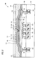
- FIG. 2 is a schematic cross-sectional view showing a schematic configuration of an image sensor for explaining an embodiment of the present invention.
- This imaging device is used by being mounted on an imaging device such as a digital camera or a digital video camera, an imaging module such as an electronic endoscope or a mobile phone, or the like.
- the image pickup device includes a plurality of organic photoelectric conversion elements configured as shown in FIG. 1, a circuit board on which a readout circuit that reads a signal corresponding to the charge generated in the photoelectric conversion layer of each organic photoelectric conversion element is formed, And a plurality of organic photoelectric conversion elements are arranged one-dimensionally or two-dimensionally on the same surface above the circuit board.
- a substrate 101 includes a substrate 101, an insulating layer 102, a connection electrode 103, a pixel electrode 104, a connection portion 105, a connection portion 106, an organic layer 107, a counter electrode 108, and a buffer layer. 109, a sealing layer 110, a color filter (CF) 111, a partition 112, a light shielding layer 113, a protective layer 114, a counter electrode voltage supply unit 115, and a readout circuit 116.
- CF color filter
- the pixel electrode 104 has the same function as the electrode 2 of the organic photoelectric conversion element 10 shown in FIG.
- the counter electrode 108 has the same function as the electrode 5 of the organic photoelectric conversion element 10 shown in FIG.
- the organic layer 107 has the same configuration as the layer provided between the electrode 2 and the electrode 5 of the organic photoelectric conversion element 10 shown in FIG.
- the sealing layer 110 has the same function as the sealing layer 6 of the organic photoelectric conversion element 10 shown in FIG.
- the pixel electrode 104, a part of the counter electrode 108 facing the pixel electrode 104, the organic layer 107 sandwiched between these electrodes, and the buffer layer 109 and the part of the sealing layer 110 facing the pixel electrode 104 are subjected to organic photoelectric conversion.
- the element is configured.
- the substrate 101 is a glass substrate or a semiconductor substrate such as Si.
- An insulating layer 102 is formed on the substrate 101.
- a plurality of pixel electrodes 104 and a plurality of connection electrodes 105 are formed on the surface of the insulating layer 102.
- the organic layer 107 is one layer common to all the organic photoelectric conversion elements provided on the plurality of pixel electrodes 104 so as to cover them.
- the counter electrode 108 is one electrode provided on the organic layer 107 and common to all organic photoelectric conversion elements.
- the counter electrode 108 is formed up to the connection electrode 103 disposed outside the organic layer 107 and is electrically connected to the connection electrode 103.
- connection part 106 is embedded in the insulating layer 102 and is a plug or the like for electrically connecting the connection electrode 103 and the counter electrode voltage supply part 115.
- the counter electrode voltage supply unit 115 is formed on the substrate 101 and applies a predetermined voltage to the counter electrode 108 via the connection unit 106 and the connection electrode 103.
- the power supply voltage is boosted by a booster circuit such as a charge pump to supply the predetermined voltage.
- the readout circuit 116 is provided on the substrate 101 corresponding to each of the plurality of pixel electrodes 104, and reads out a signal corresponding to the charge collected by the corresponding pixel electrode 104.
- the reading circuit 116 is configured by, for example, a CCD, a MOS circuit, or a TFT circuit, and is shielded from light by a light shielding layer (not shown) disposed in the insulating layer 102.
- the readout circuit 116 is electrically connected to the corresponding pixel electrode 104 via the connection unit 105.
- the buffer layer 109 is formed on the counter electrode 108 so as to cover the counter electrode 108.
- the sealing layer 110 is formed on the buffer layer 109 so as to cover the buffer layer 109.
- the color filter 111 is formed at a position facing each pixel electrode 104 on the sealing layer 110.
- the partition wall 112 is provided between the color filters 111 and is for improving the light transmission efficiency of the color filter 111.
- the light shielding layer 113 is formed in a region other than the region where the color filter 111 and the partition 112 are provided on the sealing layer 110, and prevents light from entering the organic layer 107 formed outside the effective pixel region.
- the protective layer 114 is formed on the color filter 111, the partition 112, and the light shielding layer 113, and protects the entire image sensor 100.
- the imaging device 100 when light is incident, the light is incident on the organic layer 107, and charges are generated here. Holes in the generated charges are collected by the pixel electrode 104, and a voltage signal corresponding to the amount is output to the outside of the image sensor 100 by the readout circuit 116.
- the manufacturing method of the image sensor 100 is as follows.
- connection portions 105 and 106, the plurality of connection electrodes 103, the plurality of pixel electrodes 104, and the insulating layer 102 are formed on the circuit substrate on which the counter electrode voltage supply portion 115 and the readout circuit 116 are formed.
- the plurality of pixel electrodes 104 are arranged on the surface of the insulating layer 102 in a square lattice pattern, for example.
- the organic layer 107 is formed on the plurality of pixel electrodes 104 by, for example, a vacuum heating vapor deposition method.
- the counter electrode 108 is formed on the organic layer 107 under a vacuum, for example, by sputtering.
- the buffer layer 109 and the sealing layer 110 are sequentially formed on the counter electrode 108 by, for example, a vacuum heating deposition method.
- the protective layer 114 is formed, and the imaging element 100 is completed.
- the photoelectric conversion layer 4 is a layer that includes an organic photoelectric conversion material that receives light and generates a charge corresponding to the amount of light.
- a material for the photoelectric conversion layer 4 a material having sensitivity to visible light is preferably used.
- the effect of the present invention is that the photoelectric conversion layer is a bulk hetero layer of fullerene and a p-type organic semiconductor material, the ionization potential of the photoelectric conversion layer is 5.2 eV or more and 5.6 eV or less, and the photoelectric conversion layer This can be achieved by being smaller than the ionization potential of the charge blocking layer adjacent to the conversion layer.
- the ionization potential of the photoelectric conversion layer is more preferably 5.4 eV to 5.6 eV.
- the ionization potential (Ip) of the photoelectric conversion layer in the present invention is that an organic material is deposited on a quartz substrate with a film thickness of about 100 nm, and the amount of light is 5 nW to 100 nW, using an AC-2 surface analyzer manufactured by Riken Keiki Co., Ltd. The measured value.
- the p-type organic semiconductor material (compound) constituting the photoelectric conversion layer 4 is a donor-type organic semiconductor (compound), which is mainly an organic compound represented by a hole-transporting organic compound and has a property of easily donating electrons. is there. More specifically, an organic compound having a smaller ionization potential when two organic materials are used in contact with each other. Therefore, any organic compound can be used as the donor organic compound as long as it is an electron-donating organic compound.
- the metal complex etc. which it has as can be used.
- the present invention is not limited thereto, and any organic compound having an ionization potential smaller than that of the organic compound used as the n-type organic semiconductor may be used as the donor organic semiconductor.
- Any organic dye may be used as the p-type organic semiconductor material, but preferred are a cyanine dye, a styryl dye, a hemicyanine dye, a merocyanine dye (including zero methine merocyanine (simple merocyanine)), a trinuclear merocyanine dye, Tetranuclear merocyanine dye, rhodacyanine dye, complex cyanine dye, complex merocyanine dye, allopolar dye, oxonol dye, hemioxonol dye, squalium dye, croconium dye, azamethine dye, coumarin dye, arylidene dye, anthraquinone dye, triphenylmethane dye, Azo dye, azomethine dye, spiro compound, metallocene dye, fluorenone dye, fulgide dye, perylene dye, perinone dye, phenazine dye, phenothiazin
- the photoelectric conversion layer 4 contains fullerene or a fullerene derivative.
- the fullerene, fullerene C 60, fullerene C 70, fullerene C 76, fullerene C 78, fullerene C 80, fullerene C 82, fullerene C 84, fullerene C 90, fullerene C 96, fullerene C 240, fullerene C 540, mixed Fullerene and fullerene nanotube are represented, and a fullerene derivative represents a compound having a substituent added thereto.
- the substituent for the fullerene derivative is preferably an alkyl group, an aryl group, or a heterocyclic group.
- the alkyl group is more preferably an alkyl group having 1 to 12 carbon atoms, and the aryl group and the heterocyclic group are preferably a benzene ring, naphthalene ring, anthracene ring, phenanthrene ring, fluorene ring, triphenylene ring, naphthacene ring.
- substituents may further have a substituent, and the substituents may be bonded as much as possible to form a ring.
- substituents may be bonded as much as possible to form a ring.
- you may have a some substituent and they may be the same or different.
- a plurality of substituents may be combined as much as possible to form a ring.
- the photoelectric conversion layer 4 contains fullerene or a fullerene derivative
- charges generated by photoelectric conversion can be quickly transported to the electrode 2 or the electrode 5 via the fullerene molecule or fullerene derivative molecule.
- a fullerene molecule or a fullerene derivative molecule is connected to form an electron path, the electron transport property is improved and the high-speed response of the organic photoelectric conversion element can be realized.
- the p-type organic semiconductor is reduced, the junction interface is reduced, and the exciton dissociation efficiency is lowered.
- the photoelectric conversion layer 4 when a triarylamine compound described in Japanese Patent No. 4213832 is used as a p-type organic semiconductor mixed with fullerene or a fullerene derivative, a high SN ratio of the organic photoelectric conversion element can be expressed. Is particularly preferred.
- the ratio of fullerene or fullerene derivative in the photoelectric conversion layer 4 is too large, the amount of the triarylamine compound is reduced and the amount of incident light absorbed is reduced. As a result, the photoelectric conversion efficiency decreases, so that the fullerene or fullerene derivative contained in the photoelectric conversion layer 4 preferably has a composition of 85% or less by volume.
- the p-type organic semiconductor material is preferably a compound represented by the following general formula (1).
- Z 1 represents a ring containing at least two carbon atoms and represents a 5-membered ring, a 6-membered ring, or a condensed ring containing at least one of a 5-membered ring and a 6-membered ring.
- L 1 , L 2 and L 3 each independently represent an unsubstituted methine group or a substituted methine group, D 1 represents an atomic group, and n represents an integer of 0 or more.
- Z 1 is a ring containing at least two carbon atoms and represents a 5-membered ring, a 6-membered ring, or a condensed ring containing at least one of a 5-membered ring and a 6-membered ring.
- a condensed ring containing at least one of a 5-membered ring, a 6-membered ring, and a 5-membered ring and a 6-membered ring those usually used as an acidic nucleus in a merocyanine dye are preferable. Specific examples thereof include the following: Is mentioned.
- (A) 1,3-dicarbonyl nucleus for example, 1,3-indandione nucleus, 1,3-cyclohexanedione, 5,5-dimethyl-1,3-cyclohexanedione, 1,3-dioxane-4,6- Zeon etc.
- (B) pyrazolinone nucleus for example 1-phenyl-2-pyrazolin-5-one, 3-methyl-1-phenyl-2-pyrazolin-5-one, 1- (2-benzothiazoyl) -3-methyl-2 -Pyrazolin-5-one and the like.
- (C) isoxazolinone nucleus for example, 3-phenyl-2-isoxazolin-5-one, 3-methyl-2-isoxazolin-5-one and the like.
- (D) Oxindole nucleus For example, 1-alkyl-2,3-dihydro-2-oxindole and the like.
- Examples of the derivatives include 1-alkyl compounds such as 1-methyl and 1-ethyl, 1,3-dialkyl compounds such as 1,3-dimethyl, 1,3-diethyl and 1,3-dibutyl, 1,3-diphenyl, 1,3-diaryl compounds such as 1,3-di (p-chlorophenyl) and 1,3-di (p-ethoxycarbonylphenyl), 1-alkyl-1-aryl compounds such as 1-ethyl-3-phenyl, Examples include 1,3-di (2-pyridyl) 1,3-diheterocyclic substituents and the like.
- (F) 2-thio-2,4-thiazolidinedione nucleus for example, rhodanine and its derivatives.
- the derivatives include 3-alkylrhodanine such as 3-methylrhodanine, 3-ethylrhodanine and 3-allylrhodanine, 3-arylrhodanine such as 3-phenylrhodanine, and 3- (2-pyridyl) rhodanine. And the like.
- (J) 2,4-thiazolidinedione nucleus: for example, 2,4-thiazolidinedione, 3-ethyl-2,4-thiazolidinedione, 3-phenyl-2,4-thiazolidinedione and the like.
- (M) 2-thio-2,4-imidazolidinedione (2-thiohydantoin) nucleus for example, 2-thio-2,4-imidazolidinedione, 3-ethyl-2-thio-2,4-imidazolidinedione etc.
- (N) Imidazolin-5-one nucleus for example, 2-propylmercapto-2-imidazolin-5-one and the like.
- (O) 3,5-pyrazolidinedione nucleus for example, 1,2-diphenyl-3,5-pyrazolidinedione, 1,2-dimethyl-3,5-pyrazolidinedione and the like.
- Benzothiophen-3-one nucleus for example, benzothiophen-3-one, oxobenzothiophen-3-one, dioxobenzothiophen-3-one and the like.
- Indanone nucleus for example, 1-indanone, 3-phenyl-1-indanone, 3-methyl-1-indanone, 3,3-diphenyl-1-indanone, 3,3-dimethyl-1-indanone, etc.
- the ring formed by Z 1 is preferably a 1,3-dicarbonyl nucleus, a pyrazolinone nucleus, a 2,4,6-triketohexahydropyrimidine nucleus (including a thioketone body, for example, a barbituric acid nucleus, 2-thiobarbitur tool) Acid nucleus), 2-thio-2,4-thiazolidinedione nucleus, 2-thio-2,4-oxazolidinedione nucleus, 2-thio-2,5-thiazolidinedione nucleus, 2,4-thiazolidinedione nucleus, 2, In 4-imidazolidinedione nucleus, 2-thio-2,4-imidazolidinedione nucleus, 2-imidazolin-5-one nucleus, 3,5-pyrazolidinedione nucleus, benzothiophen-3-one nucleus, indanone nucleus More preferably 1,3-dicarbonyl nucle
- L 1 , L 2 , and L 3 each independently represent an unsubstituted methine group or a substituted methine group.
- Substituted methine groups may combine to form a ring (eg, a 6-membered ring such as a benzene ring).
- the substituent of the substituted methine group includes the substituent W, it is preferable that all of L 1 , L 2 and L 3 are unsubstituted methine groups.
- L 1 to L 3 may combine with each other to form a ring, and preferred examples of the ring formed include a cyclohexene ring, a cyclopentene ring, a benzene ring, and a thiophene ring.
- N represents an integer of 0 or more, preferably 0 or more and 3 or less, more preferably 0.
- N 0 is preferable in that it has appropriate absorption in the visible region and suppresses thermal decomposition during vapor deposition.
- D 1 represents an atomic group.
- D 1 is preferably a group containing —NR a (R b ), and more preferably —NR a (R b ) represents an arylene group substituted.
- R a and R b each independently represent a hydrogen atom or a substituent.
- the arylene group represented by D 1 is preferably an arylene group having 6 to 30 carbon atoms, and more preferably an arylene group having 6 to 18 carbon atoms.
- the arylene group may have a substituent W described later, and is preferably an arylene group having 6 to 18 carbon atoms which may have an alkyl group having 1 to 4 carbon atoms. Examples include a phenylene group, a naphthylene group, an anthracenylene group, a pyrenylene group, a phenanthrenylene group, a methylphenylene group, and a dimethylphenylene group, and a phenylene group or a naphthylene group is preferable.
- R a or R b examples include the substituent W described later, and preferably an aliphatic hydrocarbon group (preferably an alkyl group or alkenyl group which may be substituted) or an aryl group (preferably a substituent). A phenyl group which may be substituted), or a heterocyclic group.
- the aryl groups represented by R a and R b are each independently preferably an aryl group having 6 to 30 carbon atoms, and more preferably an aryl group having 6 to 18 carbon atoms.
- the aryl group may have a substituent, preferably an alkyl group having 1 to 4 carbon atoms or an aryl group having 6 to 18 carbon atoms which may have an aryl group having 6 to 18 carbon atoms. is there.
- Examples include a phenyl group, a naphthyl group, an anthracenyl group, a pyrenyl group, a phenanthrenyl group, a methylphenyl group, a dimethylphenyl group, and a biphenyl group, and a phenyl group or a naphthyl group is preferable.
- the heterocyclic groups represented by R a and R b are each independently preferably a heterocyclic group having 3 to 30 carbon atoms, more preferably a heterocyclic group having 3 to 18 carbon atoms.
- the heterocyclic group may have a substituent, and preferably has an alkyl group having 1 to 4 carbon atoms or an aryl group having 6 to 18 carbon atoms. It is a group.
- the heterocyclic group represented by R a and R b is preferably a condensed ring structure, and furan ring, thiophene ring, selenophene ring, silole ring, pyridine ring, pyrazine ring, pyrimidine ring, oxazole ring, thiazole ring, triazole.
- a condensed ring structure selected from a ring, an oxadiazole ring, and a thiadiazole ring (which may be the same) is preferable.
- a bithienothiophene ring is preferred.
- the arylene group and aryl group represented by D 1 , R a and R b are preferably a benzene ring or a condensed ring structure, more preferably a condensed ring structure containing a benzene ring, a naphthalene ring, an anthracene ring, pyrene A benzene ring, a naphthalene ring or an anthracene ring is more preferable, and a benzene ring or a naphthalene ring is still more preferable.
- a halogen atom an alkyl group (including a cycloalkyl group, a bicycloalkyl group, and a tricycloalkyl group), an alkenyl group (including a cycloalkenyl group and a bicycloalkenyl group), an alkynyl group, an aryl group, and a heterocyclic group (May be referred to as a heterocyclic group), cyano group, hydroxy group, nitro group, carboxy group, alkoxy group, aryloxy group, silyloxy group, heterocyclic oxy group, acyloxy group, carbamoyloxy group, alkoxycarbonyl group, aryl Oxycarbonyl group, amino group (including anilino group), ammonio group, acylamino group, aminocarbonylamino group, alkoxycarbonylamino group, aryloxycarbonylamino group, sulfamoylamino group, alky
- the compound represented by the general formula (1) is a compound described in JP 2000-297068 A, and a compound not described in the above publication can also be produced according to the synthesis method described in the above publication. .
- the compound represented by the general formula (1) is preferably a compound represented by the general formula (2).
- Z 2 , L 21 , L 22 , L 23 , and n are synonymous with Z 1 , L 1 , L 2 , L 3 , and n in the general formula (1), and preferred examples thereof are also the same.
- D 21 represents a substituted or unsubstituted arylene group
- D 22 and D 23 each independently represents a substituted or unsubstituted aryl group or a substituted or unsubstituted heterocyclic group.
- the arylene group represented by D 21 has the same meaning as the arylene ring group represented by D 1 , and preferred examples thereof are also the same.
- the aryl group represented by D 22 and D 23 is independently the same as the heterocyclic group represented by R a and R b , and preferred examples thereof are also the same.
- D 21 and D 22 , D 21 and D 23 may each have a condensed ring structure.
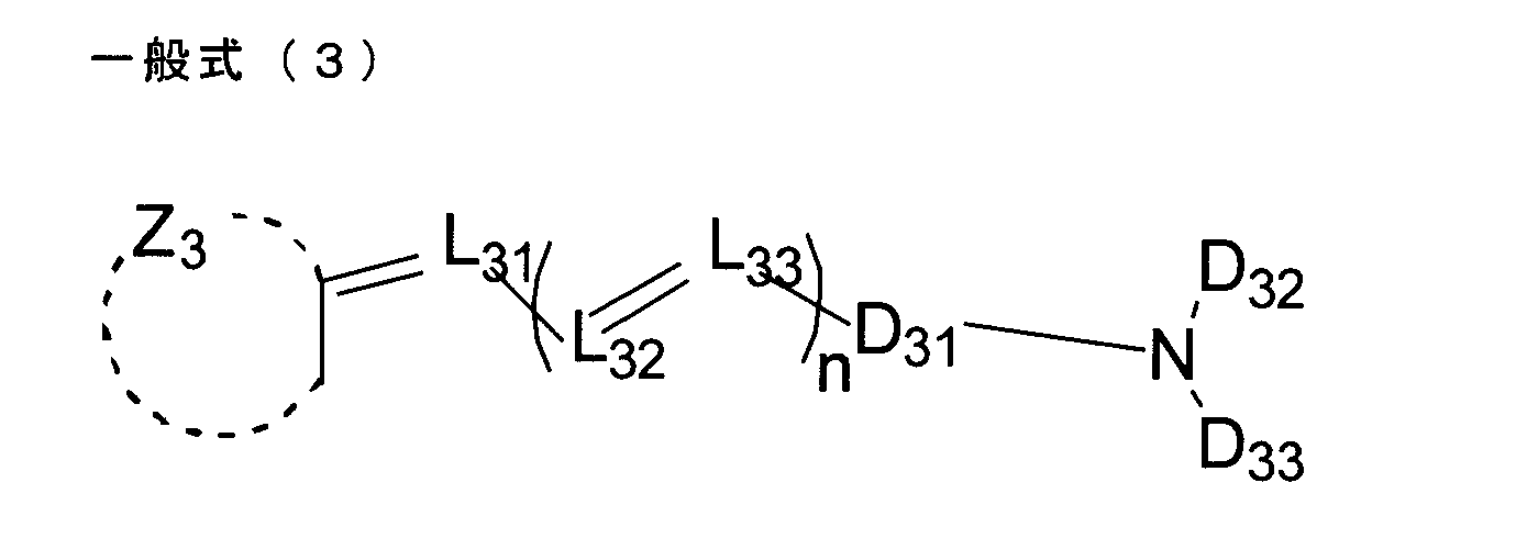
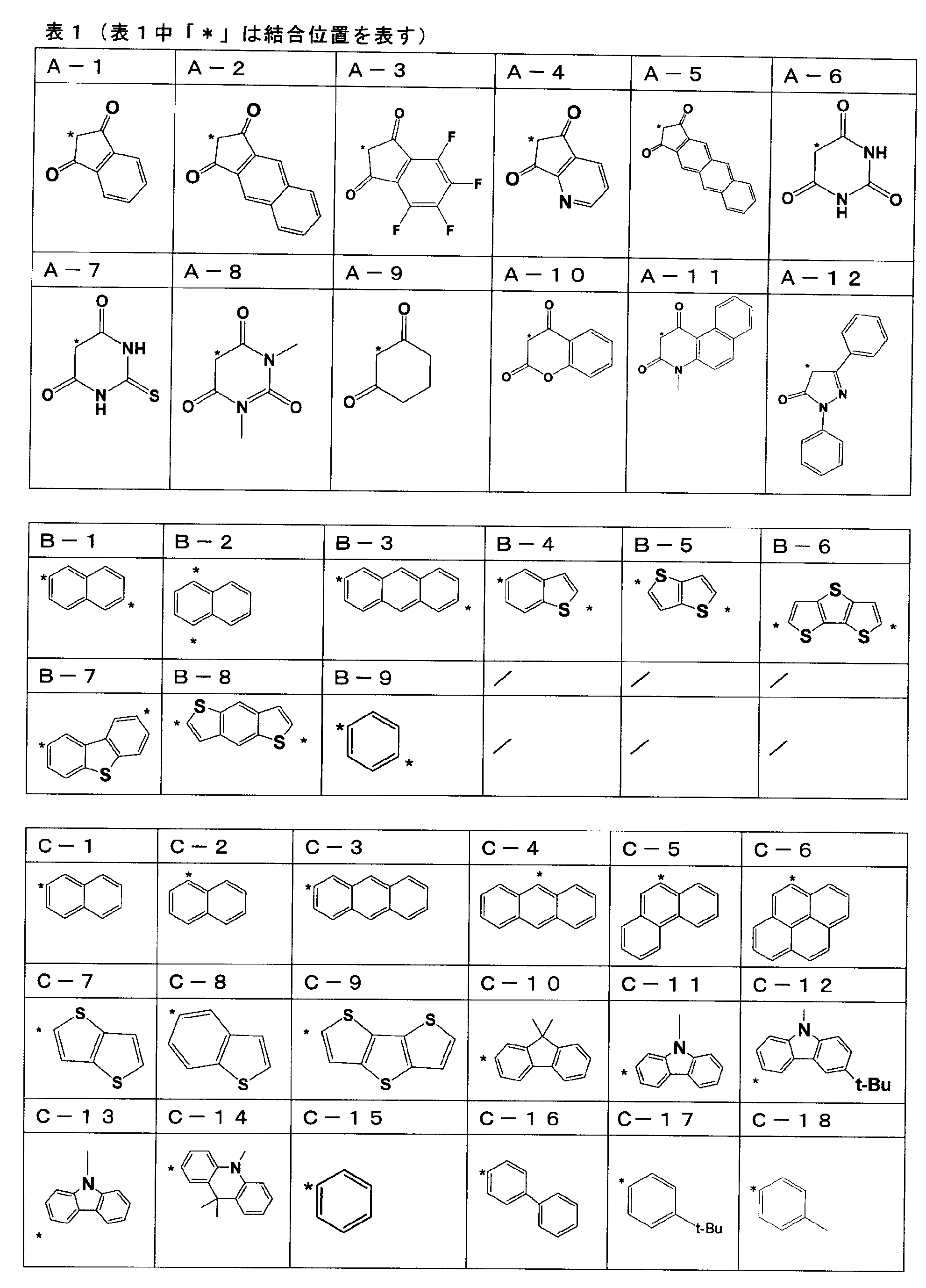
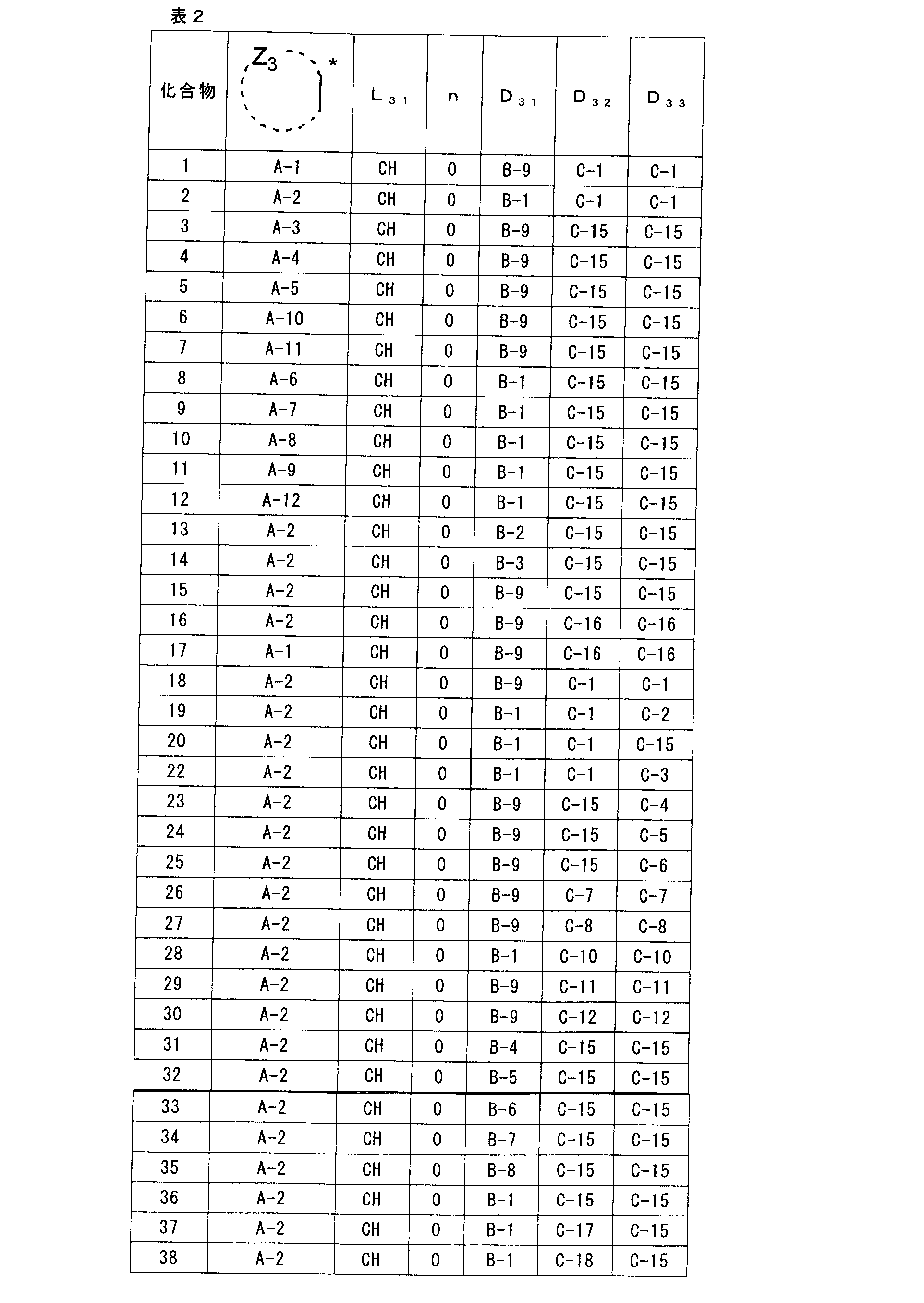
- Z 3 represents any one of A-1 to A-12 in Table 1.
- L 31 represents methylene and n represents 0.
- D 31 represents any one of B-1 to B-9, and D 32 and D 33 represent any one of C-1 to C-18.
- Z 3 is preferably A-1 or A-2, and D 32 and D 33 are selected from C-1, C-2, C-10, C-15, C-17, and C-18.
- D 31 is preferably B-1.
- D 31 and D 32 , and D 31 and D 33 may each have a condensed ring structure.
- Particularly preferred p-type organic materials include dyes or materials having no 5 or more condensed ring structures (materials having 0 to 4, preferably 1 to 3 condensed ring structures).
- a pigment-based p-type material commonly used in organic thin-film solar cells the dark current tends to increase at the pn interface, and the optical response is delayed due to trapping at the crystalline grain boundary. Therefore, it is difficult to use it for an image sensor.
- a dye-based p-type material that is difficult to crystallize, or a material that does not have five or more condensed ring structures can be preferably used for the imaging element.
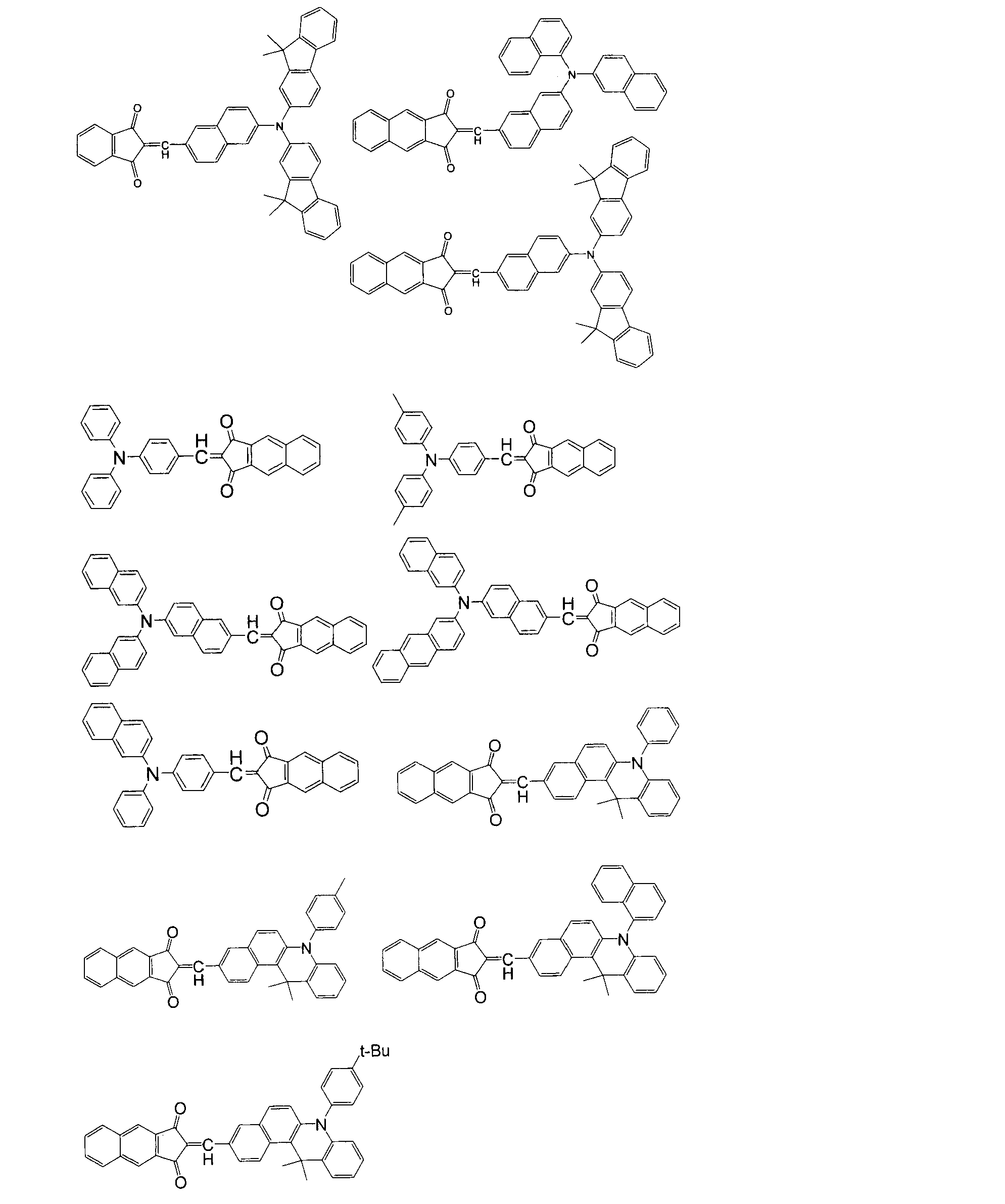
- More preferred specific examples of the compound represented by the general formula (1) are combinations of the following substituents, linking groups and partial structures in the general formula (3), but the present invention is not limited thereto. .
- A-1 to A-12, B-1 to B-9, and C-1 to C-16 are synonymous with those shown in Table 1.
- the compound represented by the general formula (1) preferably has a molecular weight of 300 or more and 1500 or less, more preferably 350 or more and 1200 or less, and more preferably 400 or more and 900 or less, from the viewpoint of film forming suitability. Further preferred. When the molecular weight is too small, the film thickness of the formed photoelectric conversion film decreases due to volatilization. Conversely, when the molecular weight is too large, vapor deposition cannot be performed, and a photoelectric conversion element cannot be manufactured.
- the compound represented by the general formula (1) has a melting point of preferably 200 ° C. or higher, more preferably 220 ° C. or higher, and further preferably 240 ° C. or higher from the viewpoint of vapor deposition stability. If the melting point is low, it melts before vapor deposition, and in addition to being unable to form a stable film, the decomposition product of the compound increases, so the photoelectric conversion performance deteriorates.
- the peak wavelength of the absorption spectrum of the compound represented by the general formula (1) is preferably 450 nm or more and 700 nm or less, more preferably 480 nm or more and 700 nm or less, and more preferably 510 nm or more and 680 nm from the viewpoint of broadly absorbing light in the visible region. More preferably, it is as follows.
- the molar extinction coefficient of peak wavelength The higher the molar extinction coefficient is, the better the compound represented by the general formula (1) is from the viewpoint of efficiently using light.
- Absorption spectrum chloroform solution
- the molar absorption coefficient preferably 20000 -1 cm -1 or more, more preferably 30000 m -1 cm -1 or more, 40000M -1 cm -1 or more Is more preferable.
- An electron-donating organic material can be used for the electron blocking layer 3.
- Porphyrin compounds triazole derivatives, oxazizazo Derivatives, imidazole derivatives, polyarylalkane derivatives, pyrazoline derivatives, pyrazolone derivatives, phenylenediamine derivatives, annealing amine derivatives, amino-substituted chalcone derivatives, oxazole derivatives, styrylanthracene derivatives, fluorenone derivatives, hydrazone derivatives, silazane derivatives, etc.
- a polymer such as phenylene vinylene, fluorene, carbazole, indole, pyrene, pyrrole, picoline, thiophene, acetylene, diacetylene, or a derivative thereof can be used. Any compound having sufficient hole transportability can be used.
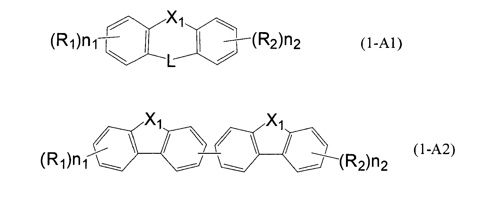
- R 1 and R 2 each independently represents a heterocyclic group which may be substituted with an alkyl group.
- X 1 each independently represents a carbon atom, a nitrogen atom, an oxygen atom, a sulfur atom, or a silicon atom, and these may further have a substituent.
- L represents a single bond, an oxygen atom, a sulfur atom, an alkylene group, an alkenylene group, a cycloalkylene group, a cycloalkenylene group, an arylene group, a divalent heterocyclic group, or an imino group, which further has a substituent. May be.
- n 1 and n 2 each independently represents an integer of 1 to 4.
- the heterocyclic group represented by R 1 and R 2 may include a condensed ring composed of 2 to 5 monocycles. Further, it preferably has 6 to 30 carbon atoms, more preferably 6 to 20 carbon atoms.
- the alkyl group that may be substituted on the heterocyclic group is preferably an alkyl group having 1 to 6 carbon atoms, and may be a linear or branched alkyl group or a cyclic alkyl group (cycloalkyl). Group), and a plurality of alkyl groups may be bonded to each other to form a ring (for example, a benzene ring), but a branched alkyl group is preferable.
- Specific examples of the alkyl group include a methyl group, an ethyl group, an isopropyl group, a t-butyl group, and a neopentyl group, and a t-butyl group is preferable.
- L represents a single bond, an oxygen atom, a sulfur atom, an alkylene group, an alkenylene group, a cycloalkylene group, a cycloalkenylene group, an arylene group, a divalent heterocyclic group, or an imino group.
- L represents a single bond, an alkylene group having 1 to 12 carbon atoms, an alkenylene group having 2 to 12 carbon atoms (for example, —CH 2 ⁇ CH 2 —), an arylene group having 6 to 14 carbon atoms (for example, 1,2-phenylene group).
- 2,3-naphthylene group a heterocyclic group having 4 to 13 carbon atoms, an oxygen atom, a sulfur atom, and a hydrocarbon group having 1 to 12 carbon atoms (preferably an aryl group or an alkyl group) (for example, phenyl)
- An imino group, a methylimino group, a t-butylimino group a single bond, an alkylene group having 1 to 6 carbon atoms (for example, a methylene group, a 1,2-ethylene group, a 1,1-dimethylmethylene group), an oxygen atom, sulfur
- An atom or an imino group having 1 to 6 carbon atoms is more preferable, and a single bond or an alkylene group having 1 to 6 carbon atoms is particularly preferable.
- L represents an alkylene group, an alkenylene group, a cycloalkylene group, a cycloalkenylene group, an arylene group, a divalent heterocyclic group, or an imino group
- these may further have a substituent.
- the further substituent include an alkyl group, a halogen atom, an aryl group, and a heterocyclic ring.
- heterocyclic group that may be substituted with the alkyl group represented by R 1 and R 2 include the following N1 to N15. N2, N4, N13, N14 and N15 are preferable.
- the substituent X 1 has an alkyl group or an aryl group.
- the alkyl group is preferably an alkyl group having 1 to 4 carbon atoms, and examples thereof include a methyl group, an ethyl group, an n-propyl group, an isopropyl group, or a t-butyl group, and more preferably a methyl group.
- the aryl group is preferably an aryl group having 6 to 20 carbon atoms.
- the aryl group may have an alkyl group, and is preferably an aryl group having 6 to 15 carbon atoms which may have an alkyl group having 1 to 4 carbon atoms.
- Examples include a phenyl group, a naphthyl group, an anthracenyl group, a 9-dimethylfluorenyl group, a methylphenyl group, a dimethylphenyl group, and the like, and a phenyl group, a naphthyl group, an anthracenyl group, and a 9-dimethylfluorenyl group are preferable.
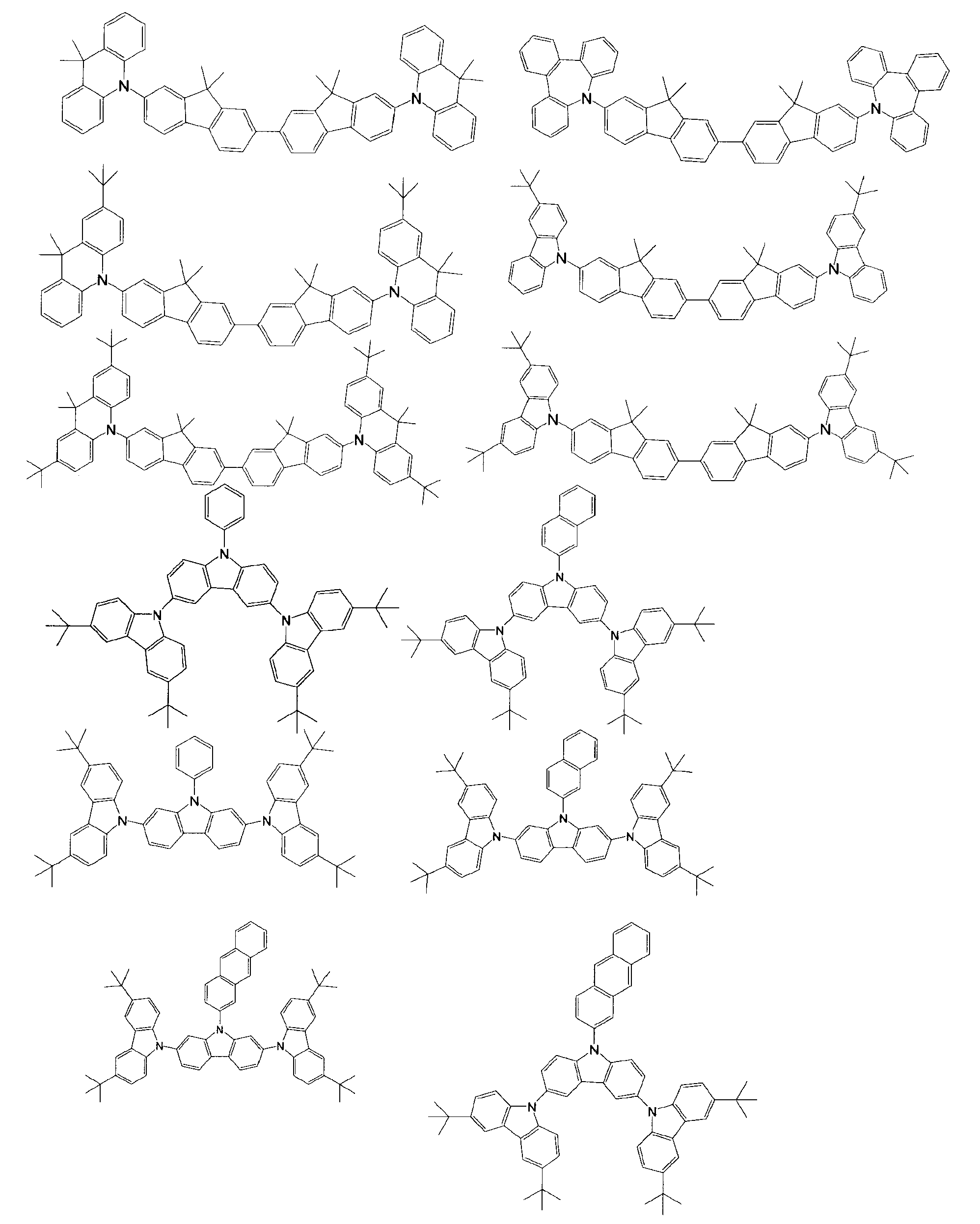
- Particularly preferable materials for the electron blocking layer include those represented by the following formula. *
- An inorganic material can be used as the electron blocking layer 3.
- an inorganic material has a dielectric constant larger than that of an organic material, when it is used for the electron blocking layer 3, a large voltage is applied to the photoelectric conversion layer 4, and the photoelectric conversion efficiency can be increased.
- Materials that can be used as the electron blocking layer 3 include calcium oxide, chromium oxide, chromium copper oxide, manganese oxide, cobalt oxide, nickel oxide, copper oxide, gallium copper oxide, strontium copper oxide, niobium oxide, molybdenum oxide, indium copper oxide, Examples include indium silver oxide and iridium oxide.
- the layer can be a layer made of an inorganic material, or in the case of a plurality of layers, one or more layers can be a layer made of an inorganic material. it can.
- Examples of the material of the electrode 2 include metals, metal oxides, metal nitrides, metal borides, organic conductive compounds, and mixtures thereof. Specific examples include tin oxide, zinc oxide, indium oxide, indium tin oxide (ITO), indium zinc oxide (IZO), indium tungsten oxide (IWO), conductive metal oxides such as titanium oxide, and metal nitrides such as TiN.
- ITO Indium Tin Oxide
- Pt platinum
- silver Ag
- Cr chromium
- Ni nickel
- Al aluminum
- ITO inorganic conductive compounds
- ITO Indium Tin Oxide
- IZO Zinc Oxide
- TiN tin oxide
- ATO antimony-doped tin oxide
- FTO fluorine-doped tin oxide
- ZO gallium-doped oxide.
- a step corresponding to the film thickness of the electrode 2 is steep at the end of the electrode 2, there are conspicuous irregularities on the surface of the electrode 2, or minute dust (particles) adhere to the electrode 2 Then, the layer on the electrode 2 becomes thinner than a desired film thickness or cracks are generated.
- the electrode 5 counter electrode 108 is formed on the layer in such a state, a pixel defect such as an increase in dark current or a short circuit occurs due to contact or electric field concentration between the electrode 2 and the electrode 5 in the defective portion. .
- the above-described defects may reduce the adhesion between the electrode 2 and the layer above it and the heat resistance of the organic photoelectric conversion element 10.
- the surface roughness Ra of the electrode 2 is preferably 0.6 nm or less.
- Examples of the material of the electrode 5 include metals, metal oxides, metal nitrides, metal borides, organic conductive compounds, and mixtures thereof. Specific examples include tin oxide, zinc oxide, indium oxide, indium tin oxide (ITO), indium zinc oxide (IZO), indium tungsten oxide (IWO), conductive metal oxides such as titanium oxide, and metal nitrides such as TiN.
- ITO Indium Tin Oxide
- Pt platinum
- silver Ag
- Cr chromium
- Ni nickel
- Al aluminum
- ITO inorganic conductive compounds
- tin oxide antimony-doped tin oxide
- FTO fluorine-doped tin oxide
- ZO gallium-doped zinc oxide
- sealing layer 6 The following conditions are required for the sealing layer 6 (sealing layer 110).
- the penetration of factors that degrade the organic photoelectric conversion material, such as water molecules, is prevented, and deterioration of the photoelectric conversion layer 4 is prevented over a long period of storage / use.
- the sealing layer 6 can be composed of a thin film made of a single material. However, by providing a different function for each layer in a multi-layer structure, the stress of the entire sealing layer 6 is reduced, and dust is generated during the manufacturing process. Such effects as the suppression of defects such as cracks and pinholes caused by the above, and the optimization of material development can be expected.
- the sealing layer 6 is formed by laminating a “sealing auxiliary layer” that has a function that is difficult to achieve on the layer that serves the original purpose of preventing the penetration of deterioration factors such as water molecules.
- a two-layer structure can be formed. Although it is possible to have three or more layers, it is preferable that the number of layers is as small as possible in consideration of manufacturing costs.
- sealing layer 6 by atomic layer deposition
- the performance of organic photoelectric conversion materials is significantly deteriorated due to the presence of deterioration factors such as water molecules. Therefore, it is necessary to cover and seal the entire photoelectric conversion layer with ceramics such as dense metal oxide / metal nitride / metal nitride oxide that does not allow water molecules to permeate, diamond-like carbon (DLC), or the like.
- ceramics such as dense metal oxide / metal nitride / metal nitride oxide that does not allow water molecules to permeate, diamond-like carbon (DLC), or the like.
- DLC diamond-like carbon
- aluminum oxide, silicon oxide, silicon nitride, silicon nitride oxide, a laminated structure thereof, a laminated structure of them and an organic polymer, or the like is used as a sealing layer by various vacuum film forming techniques.
- the imaging element 100 having a pixel size of less than 2 ⁇ m, particularly about 1 ⁇ m if the distance between the color filter 111 and the photoelectric conversion layer, that is, the film thickness of the sealing layer 110 is large, incident light is diffracted / diverged in the sealing layer 110. As a result, color mixing occurs. For this reason, the imaging element 100 having a pixel size of about 1 ⁇ m requires a sealing layer material / manufacturing method that does not deteriorate the element performance even when the film thickness of the entire sealing layer 110 is reduced.
- the atomic layer deposition (ALD) method is a kind of CVD method, and adsorption / reaction of organometallic compound molecules, metal halide molecules, and metal hydride molecules, which are thin film materials, onto the substrate surface and unreacted groups contained therein. Is a technique for forming a thin film by alternately repeating decomposition. When the thin film material reaches the substrate surface, it is in the above-mentioned low molecular state, so that the thin film can be grown in a very small space where the low molecule can enter.
- the step portion which was difficult with the conventional thin film forming method, is completely covered (the thickness of the thin film grown on the step portion is the same as the thickness of the thin film grown on the flat portion), that is, the step coverage is very high. Excellent. For this reason, steps due to structures on the substrate surface, minute defects on the substrate surface, particles adhering to the substrate surface, and the like can be completely covered, and such a step portion does not become an intrusion path for a deterioration factor of the photoelectric conversion material.
- the sealing layer 6 is formed by the atomic layer deposition method, the required sealing layer thickness can be made thinner than the conventional technique.
- the sealing layer 6 is formed by the atomic layer deposition method, a material corresponding to the ceramics preferable for the sealing layer 6 described above can be selected as appropriate.
- the photoelectric conversion layer of the present invention uses an organic photoelectric conversion material, it is limited to a material capable of growing a thin film at a relatively low temperature so that the organic photoelectric conversion material does not deteriorate.
- a dense aluminum oxide thin film can be formed at less than 200 ° C. at which the organic photoelectric conversion material does not deteriorate.
- an aluminum oxide thin film can be formed even at about 100 ° C.
- Silicon oxide and titanium oxide are also preferable because a dense thin film can be formed at less than 200 ° C., similarly to aluminum oxide, by appropriately selecting materials.
- the thin film formed by the atomic layer deposition method can achieve a high-quality thin film formation at a low temperature that is unmatched from the viewpoint of step coverage and denseness.
- the physical properties of the thin film material may be deteriorated by chemicals used in the photolithography process.
- an aluminum oxide thin film formed by atomic layer deposition is amorphous, the surface is eroded by an alkaline solution such as a developer or a stripping solution.
- a thin film having excellent chemical resistance must be formed on the aluminum oxide thin film formed by the atomic layer deposition method, that is, a sealing auxiliary layer serving as a functional layer for protecting the sealing layer 6 is provided. I need it.
- a thin film formed by a CVD method such as an atomic layer deposition method has many examples in which internal stress has a very large tensile stress, and a process in which intermittent heating and cooling are repeated like a semiconductor manufacturing process,
- the storage / use in a high-temperature / high-humidity atmosphere for a long time may cause deterioration of the thin film itself with cracks.
- a metal having excellent chemical resistance formed by a physical vapor deposition (PVD) method such as a sputtering method.
- PVD physical vapor deposition
- a configuration in which a sealing auxiliary layer including any one of ceramics such as oxide, metal nitride, and metal nitride oxide is provided is preferable.
- the first sealing layer is formed by the atomic layer deposition method, and is formed on the first sealing layer by the PVD method and is any one of metal oxide, metal nitride, and metal nitride oxide.
- One containing one is defined as a second sealing layer. If it carries out like this, it will become easy to improve the chemical resistance of the sealing layer 6 whole.
- ceramics formed by PVD methods such as sputtering often have a large compressive stress, and can cancel the tensile stress of the first sealing layer formed by atomic layer deposition. Therefore, not only the stress of the sealing layer 6 is alleviated and the reliability of the sealing layer 6 itself is increased, but the stress of the sealing layer 6 deteriorates or destroys the performance of the photoelectric conversion layer or the like. Occurrence can be remarkably suppressed.
- the first sealing layer preferably includes a second sealing layer formed by sputtering and containing any one of aluminum oxide, silicon oxide, silicon nitride, and silicon nitride oxide. .
- the first sealing layer preferably has a thickness of 0.05 ⁇ m or more and 0.2 ⁇ m or less.
- the first sealing layer preferably contains any of aluminum oxide, silicon oxide, and titanium oxide.
- Example 1 It is a photoelectric conversion element comprised of lower electrode / electron blocking layer / photoelectric conversion layer / upper electrode / sealing layer. An electron blocking layer, a photoelectric conversion layer, an upper electrode, and a sealing layer are formed in this order.
- the lower electrode is TiN.
- the electron blocking layer was formed by depositing an organic compound represented by Compound 1 with a film thickness of 100 nm at a vacuum rate of 5.0 ⁇ 10 ⁇ 4 Pa or less and a vacuum deposition method at a deposition rate of 2 ⁇ / sec.
- a film thickness of 400 nm is formed at a deposition rate of 4 liters / sec.
- the upper electrode is made of ITO with a film thickness of 10 nm by high frequency magnetron sputtering.
- As the sealing layer a laminated film of silicon monoxide, aluminum oxide, and silicon nitride was formed. Silicon monoxide was formed with a thickness of 100 nm by vacuum deposition.
- Aluminum oxide was formed to a thickness of 200 nm using an atomic layer deposition apparatus.
- Silicon nitride was formed to a thickness of 100 nm by magnetron sputtering.
- Example 2 The photoelectric conversion element of Example 2 was produced by performing the same operation as in Example 1 except that Compound 1 of Example 1 was changed to Compound 3.
- Example 3 A photoelectric conversion device of Example 3 was produced in the same manner as in Example 1 except that Compound 1 of Example 1 was changed to Compound 4.
- Comparative Example 1 A photoelectric conversion device of Comparative Example 1 was produced in the same manner as in Example 1 except that Compound 1 of Example 1 was changed to Compound 5.
- Comparative Example 2 A photoelectric conversion element of Comparative Example 2 was produced in the same manner as in Example 1 except that Compound 1 of Example 1 was changed to Compound 6.
- Table 3 shows the ionization potential (Ip) values of the layers formed using each material. Ip of each layer was measured using an AC-2 surface analyzer manufactured by Riken Keiki Co., Ltd. An organic material was formed on a quartz substrate with a film thickness of about 100 nm, and measurement was performed with a light amount of 5 nW to 50 nW.
- the device manufactured was heated to 30 ° C., 40 ° C., 60 ° C., 65 ° C. with a positive bias applied to the upper electrode side of 2.0E + 5 V / cm (2.0 ⁇ 10 5 V / cm). Adjustment was made to measure dark current and external quantum efficiency was measured. Further, after measuring the dark current and the external quantum efficiency, the device was irradiated with 1000 lux of white light for 1000 hours to perform a light resistance test. After the light resistance test, the external quantum efficiency was measured with a positive bias of 2.0E + 5 V / cm applied again to the upper electrode side.
- the dark current was measured with a source meter (6430 manufactured by Keithley) in a state where a positive bias of 2.0E + 5 V / cm was applied to the upper electrode side and the device was shielded from light.
- a source meter (6430 manufactured by Keithley)
- white light using a xenon lamp (L2195 manufactured by Hamamatsu Photonics) as a light source is made monochromatic with a spectroscope, the light amount is adjusted with an ND filter, and a positive bias of 2.0 E + 5 V / cm is applied to the upper electrode side.
- the photocurrent flowing when the device was irradiated with light was measured.
- Table 4 shows differences in dark current values at 30 ° C., 40 ° C., 60 ° C. and 65 ° C. and dark current values (current value differences) at 60 ° C. and 65 ° C., and the externals at the maximum absorption wavelength of each element before and after the light resistance test. Shows quantum efficiency.
- Examples 1 to 7 since the ionization potential of the photoelectric conversion layer is 5.2 eV or more and 5.6 eV or less, and the ionization potential of the electron blocking layer is larger than the ionization potential of the photoelectric conversion layer, the photoelectric conversion layer has high photoelectric conversion efficiency. However, there is no decrease in efficiency even after the light resistance test, and the dark current is sufficiently small in the range of 30 to 65 ° C. In Comparative Examples 1 and 2, since the ionization potential of the electron blocking layer is smaller than the ionization potential of the photoelectric conversion layer, charge boiling occurs at the interface between the photoelectric conversion layer and the electron blocking layer, and the dark current increases as the temperature rises. It has risen.
- Comparative Examples 3, 4, and 5 since the ionization potential of the photoelectric conversion layer is smaller than 5.2 eV, the boiling of electric charge occurs inside the photoelectric conversion layer, and the dark current greatly increases as the temperature rises. .
- Comparative Example 6 since the ionization potential of the electron blocking layer is larger than the ionization potential of the photoelectric conversion layer and the ionization potential of the photoelectric conversion layer is 5.2 eV or more, the dark current is small, but the ionization potential of the photoelectric conversion layer is small. Is larger than 5.6 eV, the external quantum efficiency was low before the light resistance test, and the sensitivity further decreased after the light resistance test.
- the photoelectric conversion layer is a bulk hetero layer in which the fullerene or the fullerene derivative and the p-type organic semiconductor material are mixed,
- the photoelectric conversion layer has an ionization potential of 5.2 eV or more and 5.6 eV or less, and the ionization potential of the electron blocking layer is designed to be larger than the ionization potential of the adjacent photoelectric conversion layer, thereby achieving high photoelectric conversion efficiency. It was shown that an organic photoelectric conversion element that functions as a photoelectric conversion element having a low dark current absolute value and that exhibits good characteristics at a temperature of room temperature to 60 ° C. can be realized.
- the present invention functions as a photoelectric conversion element having high photoelectric conversion efficiency, and the element exhibits a low dark current, is excellent in light resistance, and can reduce an increase in dark current due to a temperature rise.
- a photoelectric conversion element and an imaging element provided with such a photoelectric conversion element can be provided.
Landscapes
- Engineering & Computer Science (AREA)
- Chemical & Material Sciences (AREA)
- Nanotechnology (AREA)
- Physics & Mathematics (AREA)
- Mathematical Physics (AREA)
- Theoretical Computer Science (AREA)
- Crystallography & Structural Chemistry (AREA)
- Electromagnetism (AREA)
- Light Receiving Elements (AREA)
- Solid State Image Pick-Up Elements (AREA)
- Electroluminescent Light Sources (AREA)
Abstract
Description
近年、多画素化が進む中で画素サイズが小さくなっており、フォトダイオード部の面積が小さくなり、開口率の低下、集光効率の低下及びその結果である感度低下が課題となっている。開口率等を向上させる手法として、有機材料を用いた有機光電変換膜を有する固体撮像素子が検討されている。
また光電変換効率を高めるために、特許文献2ではp型有機半導体とn型有機半導体を混合した層を光電変換層(バルクへテロ層)として用いている。
すなわち、上記課題は以下の手段によって解決することができる。
〔1〕
一対の電極と、前記一対の電極の間に挟持された光電変換層を含む光電変換素子であって、前記光電変換層がフラーレン又はフラーレン誘導体とp型有機半導体材料が混合されたバルクへテロ層であり、前記光電変換層のイオン化ポテンシャルが5.2eV以上5.6eV以下であり、前記一対の電極の少なくとも一方の電極と、前記光電変換層との間に、少なくとも一層の電子ブロッキング層を備え、光電変換層と隣接する前記電子ブロッキング層のイオン化ポテンシャルが前記光電変換層のイオン化ポテンシャルよりも大きいことを特徴とする光電変換素子。
〔2〕
前記p型有機半導体材料が下記一般式(1)で表される化合物であることを特徴とする〔1〕に記載の光電変換素子。

〔3〕
前記一対の電極が導電性膜及び透明導電性膜を含み、導電性膜、電子ブロッキング層、光電変換層、及び透明導電性膜が、この順に積層されたことを特徴とする〔1〕又は〔2〕に記載の光電変換素子。
〔4〕
〔1〕~〔3〕のいずれか1つに記載の光電変換素子を含むことを特徴とする光センサ。
〔5〕
〔1〕~〔3〕のいずれか1つに記載の光電変換素子を備えたことを特徴とする撮像素子。
本発明の光電変換素子の一実施形態として、一対の電極と、前記一対の電極に挟持された光電変換層を含む光電変換素子であって、前記光電変換素子の暗電流の温度依存性が70℃以下の温度領域で50pA/(cm2×5℃)以下であることが好ましく、より好ましくは10pA/(cm2×5℃)以下である。暗電流の温度依存性が上記の範囲であれば、高温下で使用した場合の性能の低下を防ぐことができる。
他の実施形態として、一対の電極と、前記一対の電極に挟持された光電変換層を含む光電変換素子であって、65℃における前記光電変換素子の暗電流値と、60℃における前記光電変換素子の暗電流値との差が50pA/(cm2×5℃)以下であることが更に好ましく、より好ましくは10pA/(cm2×5℃)以下である。
暗電流は、KEITHLEY社の6430型ソースメータを使用し、遮光した光電変換素子にバイアス印加して、電流値を測定した。また、素子をブロックヒーターにより加熱して温度依存性を測定した。
また、本発明の光電変換素子の一実施形態として、30℃における暗電流が100pA/cm2以下であることが好ましく、より好ましくは10pA/cm2である。30℃における暗電流が100pA/cm2以下であれば、光電変換素子を用いて撮像素子を作製した場合、光電変換素子起因で発生するノイズが撮像特性に影響を与えないという効果を奏する。
図1は、本発明の一実施形態を説明するための有機光電変換素子の概略構成を示す断面模式図である。図1に示す有機光電変換素子10は、基板1と、基板1上に形成された電極2と、電極2上に形成された電子ブロッキング層3と、電子ブロッキング層3上に形成された光電変換層4と、光電変換層4上に形成された電極5と、電極5上に形成された封止層6とを備える。
光電変換素子は光電池と光センサに大別できるが、本発明の光電変換素子は光センサに適している。光センサとしては、上記光電変換素子単独で用いたものでもよいし、前記光電変換素子を直線状に配したラインセンサや、平面上に配した2次元センサの形態とすることができる。本発明の光電変換素子は、ラインセンサでは、スキャナー等の様に光学系及び駆動部を用いて光画像情報を電気信号に変換し、2次元センサでは、撮像モジュールのように光画像情報を光学系でセンサ上に結像させ電気信号に変換することで撮像素子として機能する。
光電池は発電装置であるため、光エネルギーを電気エネルギーに変換する効率が重要な性能となるが、暗所での電流である暗電流は、機能上は問題にならない。更にカラーフィルタ設置等の後段の加熱工程が必要ない。光センサは明暗信号を高い精度で電気信号に変換することが重要な性能となるため、光量を電流に変換する効率も重要な性能であるが、暗所で信号を出力するとノイズとなるため、低い暗電流が要求される。更に後段の工程に対する耐性も重要である。
次に、光電変換素子を備えた撮像素子の構成例を説明する。なお、以下に説明する構成例において、すでに説明した部材などと同等な構成・作用を有する部材等については、図中に同一符号又は相当符号を付すことにより、説明を簡略化或いは省略する。
撮像素子とは画像の光情報を電気信号に変換する素子であり、複数の光電変換素子が同一平面状でマトリクス上に配置されており、各々の光電変換素子(画素)において光信号を電気信号に変換し、その電気信号を画素ごとに逐次撮像素子外に出力できるものをいう。そのために、画素ひとつあたり、一つの光電変換素子、一つ以上のトランジスタから構成される。
光電変換層4は、光を受光して、その光量に応じた電荷を発生する有機の光電変換材料を含んで構成された層である。光電変換層4の材料としては、可視光に感度を持つ材料を用いることが好ましい。
本発明の効果は、光電変換層がフラーレンとp型有機半導材料とのバルクへテロ層であり、かつ光電変換層のイオン化ポテンシャルが、5.2eV以上5.6eV以下であり、かつ、光電変換層と隣接する電荷ブロッキング層のイオン化ポテンシャルよりも小さいことにより達成することができる。5.2eV以上であれば光電変換層での暗電流の発生を抑制することができ、5.6eV以下であれば、光電変換素子の光電変換効率と耐光性を高くすることができる。光電変換層のイオン化ポテンシャルは、5.4eV~5.6eVであることがより好ましい。
本発明における光電変換層のイオン化ポテンシャル(Ip)は、石英基板上に有機材料を約100nmの膜厚で成膜し、光量5nW~100nWで、理研計器社製AC-2表面分析装置を用いて測定した値とする。
光電変換層4を構成するp型有機半導体材料(化合物)は、ドナー性有機半導体(化合物)であり、主に正孔輸送性有機化合物に代表され、電子を供与しやすい性質がある有機化合物である。更に詳しくは2つの有機材料を接触させて用いたときにイオン化ポテンシャルの小さい方の有機化合物である。したがって、ドナー性有機化合物は、電子供与性のある有機化合物であればいずれの有機化合物も使用可能である。例えば、トリアリールアミン化合物、ベンジジン化合物、ピラゾリン化合物、スチリルアミン化合物、ヒドラゾン化合物、トリフェニルメタン化合物、カルバゾール化合物、ポリシラン化合物、チオフェン化合物、フタロシアニン化合物、シアニン化合物、メロシアニン化合物、オキソノール化合物、ポリアミン化合物、インドール化合物、ピロール化合物、ピラゾール化合物、ポリアリーレン化合物、縮合芳香族炭素環化合物(ナフタレン誘導体、アントラセン誘導体、フェナントレン誘導体、テトラセン誘導体、ピレン誘導体、ペリレン誘導体、フルオランテン誘導体)、含窒素ヘテロ環化合物を配位子として有する金属錯体等を用いることができる。なお、これに限らず、n型有機半導体として用いた有機化合物よりもイオン化ポテンシャルの小さい有機化合物であればドナー性有機半導体として用いてよい。
光電変換層4はフラーレン又はフラーレン誘導体を含む。フラーレンとは、フラーレンC60、フラーレンC70、フラーレンC76、フラーレンC78、フラーレンC80、フラーレンC82、フラーレンC84、フラーレンC90、フラーレンC96、フラーレンC240、フラーレンC540、ミックスドフラーレン、フラーレンナノチューブを表し、フラーレン誘導体とはこれらに置換基が付加された化合物のことを表す。
p型有機半導体材料は、下記一般式(1)で表される化合物であることが好ましい。

(b)ピラゾリノン核:例えば1-フェニル-2-ピラゾリン-5-オン、3-メチル-1-フェニル-2-ピラゾリン-5-オン、1-(2-ベンゾチアゾイル)-3-メチル-2-ピラゾリン-5-オン等。
(c)イソオキサゾリノン核:例えば3-フェニル-2-イソオキサゾリン-5-オン、3-メチル-2-イソオキサゾリン-5-オン等。
(d)オキシインドール核:例えば1-アルキル-2,3-ジヒドロ-2-オキシインドール等。
(e)2,4,6-トリケトヘキサヒドロピリミジン核:例えばバルビツル酸又は2-チオバルビツル酸及びその誘導体等。誘導体としては例えば1-メチル、1-エチル等の1-アルキル体、1,3-ジメチル、1,3-ジエチル、1,3-ジブチル等の1,3-ジアルキル体、1,3-ジフェニル、1,3-ジ(p-クロロフェニル)、1,3-ジ(p-エトキシカルボニルフェニル)等の1,3-ジアリール体、1-エチル-3-フェニル等の1-アルキル-1-アリール体、1,3-ジ(2―ピリジル)等の1,3位ジヘテロ環置換体等が挙げられる。
(f)2-チオ-2,4-チアゾリジンジオン核:例えばローダニン及びその誘導体等。誘導体としては例えば3-メチルローダニン、3-エチルローダニン、3-アリルローダニン等の3-アルキルローダニン、3-フェニルローダニン等の3-アリールローダニン、3-(2-ピリジル)ローダニン等の3位ヘテロ環置換ローダニン等が挙げられる。
(h)チアナフテノン核:例えば3(2H)-チアナフテノン-1,1-ジオキサイド等。
(i)2-チオ-2,5-チアゾリジンジオン核:例えば3-エチル-2-チオ-2,5-チアゾリジンジオン等。
(j)2,4-チアゾリジンジオン核:例えば2,4-チアゾリジンジオン、3-エチル-2,4-チアゾリジンジオン、3-フェニル-2,4-チアゾリジンジオン等。
(k)チアゾリン-4-オン核:例えば4-チアゾリノン、2-エチル-4-チアゾリノン等。
(l)2,4-イミダゾリジンジオン(ヒダントイン)核:例えば2,4-イミダゾリジンジオン、3-エチル-2,4-イミダゾリジンジオン等。
(m)2-チオ-2,4-イミダゾリジンジオン(2-チオヒダントイン)核:例えば2-チオ-2,4-イミダゾリジンジオン、3-エチル-2-チオ-2,4-イミダゾリジンジオン等。
(n)イミダゾリン-5-オン核:例えば2-プロピルメルカプト-2-イミダゾリン-5-オン等。
(o)3,5-ピラゾリジンジオン核:例えば1,2-ジフェニル-3,5-ピラゾリジンジオン、1,2-ジメチル-3,5-ピラゾリジンジオン等。
(p)ベンゾチオフェンー3-オン核:例えばベンゾチオフェンー3-オン、オキソベンゾチオフェンー3-オン、ジオキソベンゾチオフェンー3-オン等。
(q)インダノン核:例えば1-インダノン、3-フェニルー1-インダノン、3-メチルー1-インダノン、3,3-ジフェニルー1-インダノン、3,3-ジメチルー1-インダノン等。
L1~L3は互いに連結して環を形成しても良く、形成する環として好ましくはシクロヘキセン環、シクロペンテン環、ベンゼン環、チオフェン環等が挙げられる。
一般式(1)で表される化合物は、特開2000-297068号公報に記載の化合物であり、前記公報に記載のない化合物も、前記公報に記載の合成方法に準じて製造することができる。
一般式(1)で表される化合物は一般式(2)で表される化合物であることが好ましい。
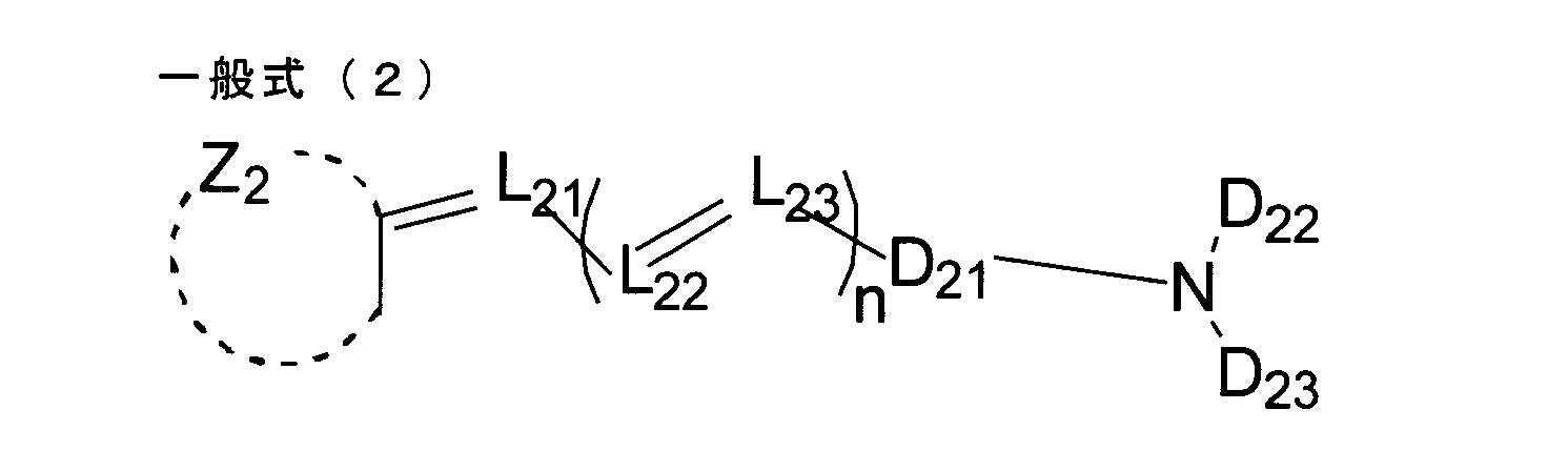
D22、及びD23が表すアリール基としては、それぞれ独立に、Ra、及びRbが表すヘテロ環基と同義であり、その好ましい例も同様である。
D21とD22、D21とD23はそれぞれ縮環構造をとっても良い。
以下にp型有機材料の具体例を示すが、本発明はこれらに限定されるものではない。
一般式(1)で表される化合物は、成膜適性の観点から、分子量が300以上1500以下であることが好ましく、350以上1200以下であることがより好ましく、400以上900以下であることが更に好ましい。分子量が小さすぎる場合では、成膜した光電変換膜の膜厚が揮発により減少してしまい、逆に分子量が大きすぎる場合では蒸着ができず、光電変換素子を作製できない。
一般式(1)で表される化合物は、蒸着安定性の観点から、融点が200℃以上であることが好ましく、220℃以上がより好ましく、240℃以上が更に好ましい。融点が低いと蒸着前に融解してしまい、安定に成膜できないことに加え、化合物の分解物が多くなるため、光電変換性能が劣化する。
一般式(1)で表される化合物の吸収スペクトルのピーク波長は、可視領域の光を幅広く吸収するという観点から450nm以上700nm以下であることが好ましく、480nm以上700nm以下がより好ましく、510nm以上680nm以下であることが更に好ましい。
一般式(1)で表される化合物は、光を効率よく利用する観点から、モル吸光係数は高ければ高いほどよい。吸収スペクトル(クロロホルム溶液)が、波長400nmから700nmまでの可視領域において、モル吸光係数は20000M-1cm-1以上が好ましく、30000M-1cm-1以上がより好ましく、40000M-1cm-1以上が更に好ましい。
[電子ブロッキング層]
電子ブロッキング層3には、電子供与性有機材料を用いることができる。具体的には、低分子材料では、N,N’-ビス(3-メチルフェニル)-(1,1’-ビフェニル)-4,4’-ジアミン(TPD)や4,4’-ビス[N-(ナフチル)-N-フェニル-アミノ]ビフェニル(α-NPD)等の芳香族ジアミン化合物、オキサゾール、オキサジアゾール、トリアゾール、イミダゾール、イミダゾロン、スチルベン誘導体、ピラゾリン誘導体、テトラヒドロイミダゾール、ポリアリールアルカン、ブタジエン、4,4’,4”-トリス(N-(3-メチルフェニル)N-フェニルアミノ)トリフェニルアミン(m-MTDATA)、ポルフィン、テトラフェニルポルフィン銅、フタロシアニン、銅フタロシアニン、チタニウムフタロシアニンオキサイド等のポリフィリン化合物、トリアゾール誘導体、オキサジザゾール誘導体、イミダゾール誘導体、ポリアリールアルカン誘導体、ピラゾリン誘導体、ピラゾロン誘導体、フェニレンジアミン誘導体、アニールアミン誘導体、アミノ置換カルコン誘導体、オキサゾール誘導体、スチリルアントラセン誘導体、フルオレノン誘導体、ヒドラゾン誘導体、シラザン誘導体などを用いることができ、高分子材料では、フェニレンビニレン、フルオレン、カルバゾール、インドール、ピレン、ピロール、ピコリン、チオフェン、アセチレン、ジアセチレン等の重合体や、その誘導体を用いることができる。電子供与性化合物でなくとも、充分な正孔輸送性を有する化合物であれば用いることは可能である。
Lがアルキレン基、アルケニレン基、シクロアルキレン基、シクロアルケニレン基、アリーレン基、2価の複素環基、又はイミノ基を表す場合、これらは更に置換基を有していてもよい。該更なる置換基としては、アルキル基、ハロゲン原子、アリール基、ヘテロ環が挙げられる。

アルキル基としては、好ましくは炭素数1~4のアルキル基であり、例えば、メチル基、エチル基、n-プロピル基、イゾプロピル基、又はt-ブチル基が挙げられ、メチル基であることがより好ましい。
アリール基としては、好ましくは炭素数6~20のアリール基である。該アリール基は、アルキル基を有していてもよく、好ましくは炭素数1~4のアルキル基を有していてもよい炭素数6~15のアリール基である。例えば、フェニル基、ナフチル基、アントラセニル基、9-ジメチルフルオレニル基、メチルフェニル基、ジメチルフェニル基等が挙げられ、フェニル基、ナフチル基、アントラセニル基、9-ジメチルフルオレニル基好ましい。



電極2(画素電極104)の材料としては、例えば、金属、金属酸化物、金属窒化物、金属硼化物、有機導電性化合物、これらの混合物等が挙げられる。具体例としては、酸化錫、酸化亜鉛、酸化インジウム、酸化インジウム錫(ITO)、酸化インジウム亜鉛(IZO)、酸化インジウムタングステン(IWO)、酸化チタン等の導電性金属酸化物、TiN等の金属窒化物、金(Au)、白金(Pt)、銀(Ag)、クロム(Cr)、ニッケル(Ni)、アルミニウム(Al)等の金属、更にこれらの金属と導電性金属酸化物との混合物又は積層物、ポリアニリン、ポリチオフェン、ポリピロール等の有機導電性化合物、これらとITOとの積層物、などが挙げられる。透明導電膜の材料として特に好ましいのは、ITO、IZO、TiN、酸化錫、アンチモンドープ酸化錫(ATO)、弗素ドープ酸化錫(FTO)、酸化亜鉛、アンチモンドープ酸化亜鉛(AZO)、ガリウムドープ酸化亜鉛(GZO)のいずれかの材料である。
電極5(対向電極108)の材料としては、例えば、金属、金属酸化物、金属窒化物、金属硼化物、有機導電性化合物、これらの混合物等が挙げられる。具体例としては、酸化錫、酸化亜鉛、酸化インジウム、酸化インジウム錫(ITO)、酸化インジウム亜鉛(IZO)、酸化インジウムタングステン(IWO)、酸化チタン等の導電性金属酸化物、TiN等の金属窒化物、金(Au)、白金(Pt)、銀(Ag)、クロム(Cr)、ニッケル(Ni)、アルミニウム(Al)等の金属、更にこれらの金属と導電性金属酸化物との混合物又は積層物、ポリアニリン、ポリチオフェン、ポリピロール等の有機導電性化合物、これらとITOとの積層物、などが挙げられる。透明導電膜の材料として特に好ましいのは、ITO、IZO、酸化錫、アンチモンドープ酸化錫(ATO)、弗素ドープ酸化錫(FTO)、酸化亜鉛、アンチモンドープ酸化亜鉛(AZO)、ガリウムドープ酸化亜鉛(GZO)のいずれかの材料である。
封止層6(封止層110)としては次の条件が求められる。
第一に、素子の各製造工程において溶液、プラズマなどに含まれる有機の光電変換材料を劣化させる因子の浸入を阻止して光電変換層を保護することが挙げられる。
第二に、素子の製造後に、水分子などの有機の光電変換材料を劣化させる因子の浸入を阻止して、長期間の保存/使用にわたって、光電変換層4の劣化を防止する。
第三に、封止層6を形成する際は既に形成された光電変換層を劣化させない。
第四に、入射光は封止層6を通じて光電変換層4に到達するので、光電変換層4で検知する波長の光に対して封止層6は透明でなくてはならない。
有機光電変換材料は水分子などの劣化因子の存在で顕著にその性能が劣化してしまう。そのために、水分子を浸透させない緻密な金属酸化物・金属窒化物・金属窒化酸化物などセラミクスやダイヤモンド状炭素(DLC)などで光電変換層全体を被覆して封止することが必要である。従来から、酸化アルミニウム、酸化珪素、窒化珪素、窒化酸化珪素やそれらの積層構成、それらと有機高分子の積層構成などを封止層として、各種真空成膜技術で形成されている。もっとも、これら従来の封止層は、基板表面の構造物、基板表面の微小欠陥、基板表面に付着したパーティクルなどによる段差において、薄膜の成長が困難なので(段差が影になるので)平坦部と比べて膜厚が顕著に薄くなる。このために段差部分が劣化因子の浸透する経路になってしまう。この段差を封止層で完全に被覆するには、平坦部において1μm以上の膜厚になるように成膜して、封止層全体を厚くする必要がある。
原子層堆積法により形成した薄膜は、段差被覆性、緻密性という観点からは比類なく良質な薄膜形成を低温で達成できる。もっとも、薄膜材料の物性が、フォトリソグラフィ工程で使用する薬品で劣化してしまうことがある。例えば、原子層堆積法で成膜した酸化アルミニウム薄膜は非晶質なので、現像液や剥離液のようなアルカリ溶液で表面が侵食されてしまう。この場合は、原子層堆積法で形成した酸化アルミニウム薄膜上に、耐薬品性に優れる薄膜を形成しなくてはならず、すなわち、封止層6を保護する機能層となる封止補助層が必要になる。
下部電極/電子ブロッキング層/光電変換層/上部電極/封止層で構成された光電変換素子である。電子ブロッキング層、光電変換層、上部電極、封止層の順に形成する。下部電極はTiNである。電子ブロッキング層は化合物1で示される有機化合物を5.0×10-4Pa以下の真空度で、真空蒸着法により、2Å/secの蒸着速度で、100nmの膜厚で形成した。光電変換層は化合物2で示される有機化合物とフラーレンC60の混合膜(化合物2:C60=1:2(体積比))を、5.0×10-4Pa以下の真空中で共蒸着により、4Å/secの蒸着速度で400nmの膜厚で形成する。上部電極はITOを高周波マグネトロンスパッタにより、10nmの膜厚で形成する。封止層は、一酸化珪素、酸化アルミニウム、窒化珪素の積層膜を形成した。一酸化珪素は、真空蒸着により100nmの膜厚で形成した。酸化アルミニウムは原子層堆積装置を使用し、200nmの膜厚で形成した。窒化珪素はマグネトロンスパッタにより、100nmの膜厚で形成した。
実施例1の化合物1を化合物3に変更した以外は実施例1と同様の操作を行い実施例2の光電変換素子を作製した。
実施例1の化合物1を化合物4に変更した以外は実施例1と同様の操作を行い実施例3の光電変換素子を作製した。
実施例1の光電変換層を化合物2で示される有機化合物とフラーレンC60の混合膜(化合物2:C60=1:3(体積比))に変更した以外は実施例1と同様の操作を行い実施例4の光電変換素子を作製した。
実施例3の光電変換層を化合物7で示される有機化合物とフラーレンC60の混合膜(化合物7:C60=1:2(体積比))に変更した以外は実施例3と同様の操作を行い実施例5の光電変換素子を作製した。
実施例3の光電変換層を化合物8で示される有機化合物とフラーレンC60の混合膜(化合物8:C60=1:2(体積比))に変更した以外は実施例3と同様の操作を行い実施例6の光電変換素子を作製した。
実施例1の光電変換層を化合物13で示される有機化合物とフラーレンC60の混合膜(化合物13:C60=1:2(体積比))に変更した以外は実施例1と同様の操作を行い実施例7の光電変換素子を作製した。
実施例1の化合物1を化合物5に変更した以外は実施例1と同様の操作を行い比較例1の光電変換素子を作製した。
実施例1の化合物1を化合物6に変更した以外は実施例1と同様の操作を行い比較例2の光電変換素子を作製した。
実施例1の光電変換層を化合物9で示される有機化合物とフラーレンC60の混合膜(化合物9:C60=1:2(体積比))に変更した以外は実施例1と同様の操作を行い比較例3の光電変換素子を作製した。
実施例3の光電変換層を化合物10で示される有機化合物とフラーレンC60の混合膜(化合物10:C60=1:2(体積比))に変更した以外は実施例3と同様の操作を行い比較例4の光電変換素子を作製した。
実施例1の光電変換層を化合物11で示される有機化合物とフラーレンC60の混合膜(化合物11:C60=1:2(体積比))に変更した以外は実施例1と同様の操作を行い比較例5の光電変換素子を作製した。
実施例1の光電変換層を化合物12で示される有機化合物とフラーレンC60の混合膜(化合物12:C60=1:2(体積比))に変更した以外は実施例1と同様の操作を行い比較例6の光電変換素子を作製した。


各層のIpは理研計器社製AC-2表面分析装置を用いて測定した。石英基板上に有機材料を約100nmの膜厚で成膜し、光量5nW~50nWで測定を行った。

表4に、30℃、40℃、60℃、65℃における暗電流値及び60℃、65℃における暗電流値の差(電流値差)、及び耐光試験前後の各素子の最大吸収波長における外部量子効率を示す。
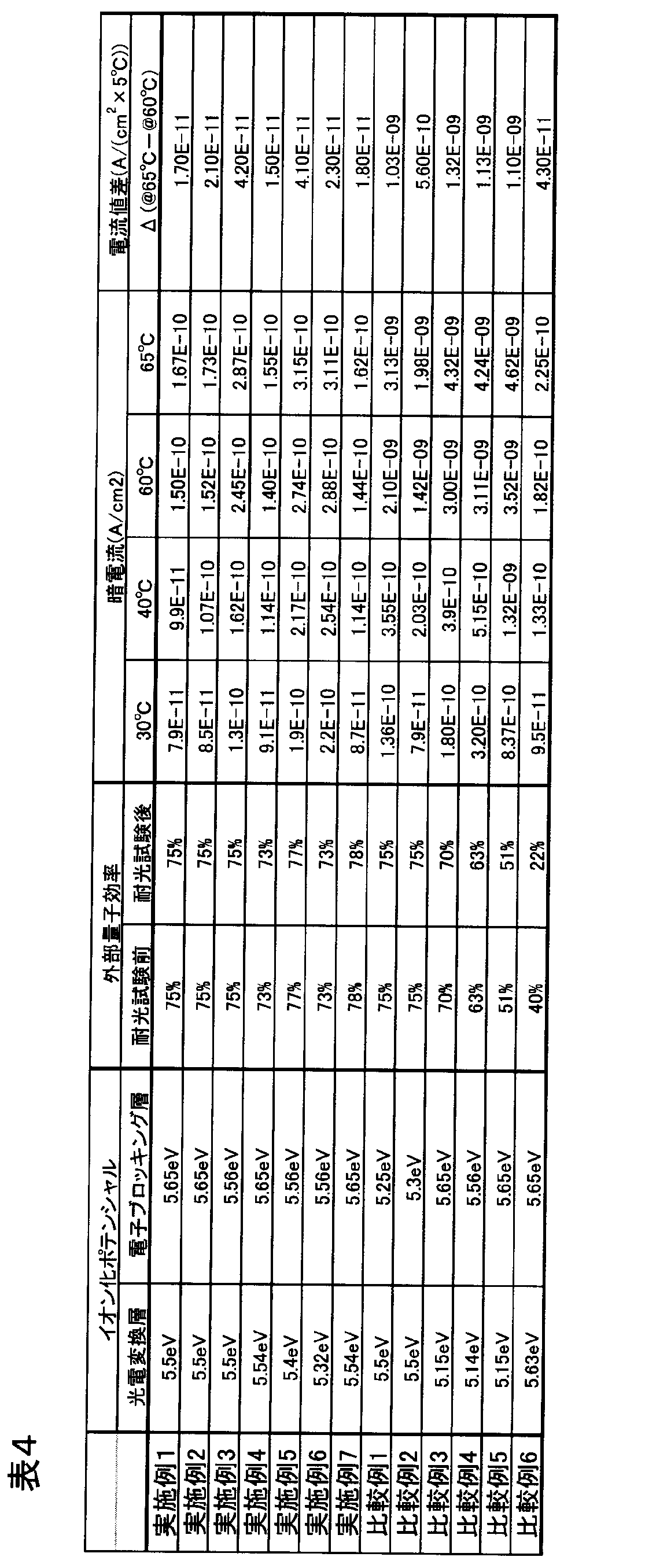
本出願は、2010年3月31日出願の日本特許出願(特願2010-084407)及び、2010年11月5日出願の日本特許出願(特願2010-249209)に基づくものであり、その内容はここに参照として取り込まれる。
1 基板
2 電極
3 電子ブロッキング層
4 光電変換層
5 電極
6 封止層
100 撮像素子
100 撮像素子
Claims (5)
- 一対の電極と、前記一対の電極の間に挟持された光電変換層を含む光電変換素子であって、前記光電変換層がフラーレン又はフラーレン誘導体とp型有機半導体材料が混合されたバルクへテロ層であり、前記光電変換層のイオン化ポテンシャルが5.2eV以上5.6eV以下であり、前記一対の電極の少なくとも一方の電極と、前記光電変換層との間に、少なくとも一層の電子ブロッキング層を備え、光電変換層と隣接する前記電子ブロッキング層のイオン化ポテンシャルが前記光電変換層のイオン化ポテンシャルよりも大きいことを特徴とする光電変換素子。
- 前記p型有機半導体材料が下記一般式(1)で表される化合物であることを特徴とする請求項1に記載の光電変換素子。
一般式(1)

- 前記一対の電極が導電性膜及び透明導電性膜を含み、導電性膜、電子ブロッキング層、光電変換層、及び透明導電性膜が、この順に積層されたことを特徴とする、請求項1又は2に記載の光電変換素子。
- 請求項1~3のいずれか1項に記載の光電変換素子を含むことを特徴とする光センサ。
- 請求項1~3のいずれか1項に記載の光電変換素子を備えたことを特徴とする撮像素子。
Priority Applications (2)
| Application Number | Priority Date | Filing Date | Title |
|---|---|---|---|
| US13/638,648 US8860016B2 (en) | 2010-03-31 | 2011-03-24 | Photoelectric conversion device and imaging device |
| KR1020127025578A KR101583585B1 (ko) | 2010-03-31 | 2011-03-24 | 광전 변환 소자 및 촬상 소자 |
Applications Claiming Priority (4)
| Application Number | Priority Date | Filing Date | Title |
|---|---|---|---|
| JP2010084407 | 2010-03-31 | ||
| JP2010-084407 | 2010-03-31 | ||
| JP2010249209A JP5264865B2 (ja) | 2010-03-31 | 2010-11-05 | 光電変換素子及び撮像素子 |
| JP2010-249209 | 2010-11-05 |
Publications (1)
| Publication Number | Publication Date |
|---|---|
| WO2011125526A1 true WO2011125526A1 (ja) | 2011-10-13 |
Family
ID=44762480
Family Applications (1)
| Application Number | Title | Priority Date | Filing Date |
|---|---|---|---|
| PCT/JP2011/057250 Ceased WO2011125526A1 (ja) | 2010-03-31 | 2011-03-24 | 光電変換素子及び撮像素子 |
Country Status (4)
| Country | Link |
|---|---|
| US (1) | US8860016B2 (ja) |
| JP (1) | JP5264865B2 (ja) |
| KR (1) | KR101583585B1 (ja) |
| WO (1) | WO2011125526A1 (ja) |
Cited By (2)
| Publication number | Priority date | Publication date | Assignee | Title |
|---|---|---|---|---|
| WO2012032990A1 (ja) * | 2010-09-08 | 2012-03-15 | 富士フイルム株式会社 | 光電変換材料、該材料を含む膜、光電変換素子、光電変換素子の製造方法、光電変換素子の使用方法、光センサ、撮像素子 |
| US11758745B2 (en) | 2019-04-18 | 2023-09-12 | Semiconductor Energy Laboratory Co., Ltd. | Solid-state relay and semiconductor device |
Families Citing this family (20)
| Publication number | Priority date | Publication date | Assignee | Title |
|---|---|---|---|---|
| JP5662893B2 (ja) * | 2011-07-25 | 2015-02-04 | 富士フイルム株式会社 | 光電変換素子用蒸着材料及び光電変換素子、センサ、撮像素子 |
| US9293722B2 (en) | 2012-05-01 | 2016-03-22 | Sony Corporation | Solid-state image pickup device, method of manufacturing the same, and electronic apparatus |
| JP6025243B2 (ja) * | 2012-05-10 | 2016-11-16 | 富士フイルム株式会社 | 光電変換素子及びそれを用いた撮像素子 |
| JP6077426B2 (ja) * | 2012-09-28 | 2017-02-08 | 富士フイルム株式会社 | 光電変換素子およびその使用方法、光センサ、撮像素子 |
| JP6059697B2 (ja) * | 2013-09-30 | 2017-01-11 | 富士フイルム株式会社 | 光電変換素子および撮像素子 |
| JP6047109B2 (ja) | 2014-02-14 | 2016-12-21 | 富士フイルム株式会社 | 光電変換素子、光センサおよび撮像素子 |
| WO2016017350A1 (ja) * | 2014-07-31 | 2016-02-04 | 富士フイルム株式会社 | 光電変換素子および撮像素子 |
| KR102491494B1 (ko) | 2015-09-25 | 2023-01-20 | 삼성전자주식회사 | 유기 광전 소자용 화합물 및 이를 포함하는 유기 광전 소자 및 이미지 센서 |
| KR102547655B1 (ko) | 2015-11-18 | 2023-06-23 | 삼성전자주식회사 | 이미지 센서 및 이를 포함하는 전자 장치 |
| KR102529631B1 (ko) | 2015-11-30 | 2023-05-04 | 삼성전자주식회사 | 유기 광전 소자 및 이미지 센서 |
| KR102557864B1 (ko) | 2016-04-06 | 2023-07-19 | 삼성전자주식회사 | 화합물, 및 이를 포함하는 유기 광전 소자, 이미지 센서 및 전자 장치 |
| US10236461B2 (en) | 2016-05-20 | 2019-03-19 | Samsung Electronics Co., Ltd. | Organic photoelectronic device and image sensor |
| KR102605375B1 (ko) | 2016-06-29 | 2023-11-22 | 삼성전자주식회사 | 유기 광전 소자 및 이미지 센서 |
| KR102589215B1 (ko) | 2016-08-29 | 2023-10-12 | 삼성전자주식회사 | 유기 광전 소자, 이미지 센서 및 전자 장치 |
| JP2018123083A (ja) * | 2017-01-31 | 2018-08-09 | 出光興産株式会社 | 新規アントラセン誘導体、有機エレクトロルミネッセンス素子用材料、有機エレクトロルミネッセンス素子用材料溶液、有機エレクトロルミネッセンス素子及び電子機器 |
| TWI782937B (zh) * | 2017-04-10 | 2022-11-11 | 日商松下知識產權經營股份有限公司 | 攝像裝置 |
| US11145822B2 (en) | 2017-10-20 | 2021-10-12 | Samsung Electronics Co., Ltd. | Compound and photoelectric device, image sensor, and electronic device including the same |
| EP3832725A4 (en) * | 2018-07-31 | 2021-08-25 | Sony Semiconductor Solutions Corporation | IMAGING ELEMENT AND IMAGING DEVICE |
| JP2022035072A (ja) * | 2020-08-20 | 2022-03-04 | 三菱ケミカル株式会社 | 正孔輸送層及び光電変換層を有する積層体、光電変換素子及び光検出デバイス |
| KR102939978B1 (ko) | 2020-12-24 | 2026-03-16 | 후지필름 가부시키가이샤 | 광전 변환 소자, 촬상 소자, 광 센서, 화합물 |
Citations (2)
| Publication number | Priority date | Publication date | Assignee | Title |
|---|---|---|---|---|
| JP2007088033A (ja) * | 2005-09-20 | 2007-04-05 | Fujifilm Corp | 有機光電変換素子、および撮像素子 |
| US20090223566A1 (en) * | 2008-03-07 | 2009-09-10 | Fujifilm Corporation | Photoelectric conversion element and imaging device |
Family Cites Families (4)
| Publication number | Priority date | Publication date | Assignee | Title |
|---|---|---|---|---|
| JP2004165516A (ja) | 2002-11-14 | 2004-06-10 | Matsushita Electric Works Ltd | 有機太陽電池 |
| JP4914597B2 (ja) | 2005-10-31 | 2012-04-11 | 富士フイルム株式会社 | 光電変換素子及び撮像素子、並びに、これらに電場を印加する方法 |
| JP2009049278A (ja) | 2007-08-22 | 2009-03-05 | Fujifilm Corp | 光電変換素子、光電変換素子の製造方法、固体撮像素子 |
| JP5216279B2 (ja) | 2007-08-23 | 2013-06-19 | 富士フイルム株式会社 | 有機半導体材料、該材料を含む膜、有機電子デバイス及び赤外色素組成物 |
-
2010
- 2010-11-05 JP JP2010249209A patent/JP5264865B2/ja active Active
-
2011
- 2011-03-24 WO PCT/JP2011/057250 patent/WO2011125526A1/ja not_active Ceased
- 2011-03-24 US US13/638,648 patent/US8860016B2/en active Active
- 2011-03-24 KR KR1020127025578A patent/KR101583585B1/ko active Active
Patent Citations (2)
| Publication number | Priority date | Publication date | Assignee | Title |
|---|---|---|---|---|
| JP2007088033A (ja) * | 2005-09-20 | 2007-04-05 | Fujifilm Corp | 有機光電変換素子、および撮像素子 |
| US20090223566A1 (en) * | 2008-03-07 | 2009-09-10 | Fujifilm Corporation | Photoelectric conversion element and imaging device |
Cited By (3)
| Publication number | Priority date | Publication date | Assignee | Title |
|---|---|---|---|---|
| WO2012032990A1 (ja) * | 2010-09-08 | 2012-03-15 | 富士フイルム株式会社 | 光電変換材料、該材料を含む膜、光電変換素子、光電変換素子の製造方法、光電変換素子の使用方法、光センサ、撮像素子 |
| US9349965B2 (en) | 2010-09-08 | 2016-05-24 | Fujifilm Corporation | Photoelectric conversion material, film containing the material, photoelectric conversion device, method for preparing photoelectric conversion device, method for using photoelectric conversion device, photosensor and imaging device |
| US11758745B2 (en) | 2019-04-18 | 2023-09-12 | Semiconductor Energy Laboratory Co., Ltd. | Solid-state relay and semiconductor device |
Also Published As
| Publication number | Publication date |
|---|---|
| KR20130018730A (ko) | 2013-02-25 |
| US8860016B2 (en) | 2014-10-14 |
| KR101583585B1 (ko) | 2016-01-08 |
| JP2011228623A (ja) | 2011-11-10 |
| JP5264865B2 (ja) | 2013-08-14 |
| US20130020566A1 (en) | 2013-01-24 |
Similar Documents
| Publication | Publication Date | Title |
|---|---|---|
| JP5264865B2 (ja) | 光電変換素子及び撮像素子 | |
| JP6059697B2 (ja) | 光電変換素子および撮像素子 | |
| JP5323025B2 (ja) | 固体撮像素子 | |
| JP5270642B2 (ja) | 光電変換素子及び撮像素子 | |
| JP5557663B2 (ja) | 光電変換素子及びその製造方法、光センサ、並びに撮像素子及びそれらの駆動方法 | |
| JP4825924B2 (ja) | 光電変換素子及びその製造方法、光センサ、並びに撮像素子及びそれらの駆動方法 | |
| JP6046649B2 (ja) | 光電変換素子及びそれを用いた撮像素子 | |
| JP6010514B2 (ja) | 光電変換素子および撮像素子 | |
| JP5288640B2 (ja) | 撮像素子及びその製造方法 | |
| JP5814293B2 (ja) | 光電変換素子および撮像素子、ならびに、光電変換素子の製造方法および撮像素子の製造方法 | |
| JP5806176B2 (ja) | 固体撮像素子および固体撮像素子の製造方法 | |
| JP5824436B2 (ja) | 光電変換素子及びそれを用いた撮像素子 | |
| US20140179055A1 (en) | Method for producing photoelectric conversion element and method for producing imaging device | |
| JP5651507B2 (ja) | 有機光電変換素子の製造方法、有機光電変換素子、撮像素子、撮像装置 | |
| JP2013055248A (ja) | 光電変換素子の製造方法 | |
| KR20110104910A (ko) | 유기 광전 변환 소자의 제조 방법, 유기 광전 변환 소자, 촬상 소자, 및 촬상 장치 |
Legal Events
| Date | Code | Title | Description |
|---|---|---|---|
| 121 | Ep: the epo has been informed by wipo that ep was designated in this application |
Ref document number: 11765427 Country of ref document: EP Kind code of ref document: A1 |
|
| ENP | Entry into the national phase |
Ref document number: 20127025578 Country of ref document: KR Kind code of ref document: A |
|
| NENP | Non-entry into the national phase |
Ref country code: DE |
|
| WWE | Wipo information: entry into national phase |
Ref document number: 13638648 Country of ref document: US |
|
| 122 | Ep: pct application non-entry in european phase |
Ref document number: 11765427 Country of ref document: EP Kind code of ref document: A1 |