WO2011125440A1 - 分光モジュール - Google Patents
分光モジュール Download PDFInfo
- Publication number
- WO2011125440A1 WO2011125440A1 PCT/JP2011/056247 JP2011056247W WO2011125440A1 WO 2011125440 A1 WO2011125440 A1 WO 2011125440A1 JP 2011056247 W JP2011056247 W JP 2011056247W WO 2011125440 A1 WO2011125440 A1 WO 2011125440A1
- Authority
- WO
- WIPO (PCT)
- Prior art keywords
- light
- unit
- spectroscopic
- main body
- layer
- Prior art date
- Legal status (The legal status is an assumption and is not a legal conclusion. Google has not performed a legal analysis and makes no representation as to the accuracy of the status listed.)
- Ceased
Links
Images


Classifications
-
- G—PHYSICS
- G01—MEASURING; TESTING
- G01J—MEASUREMENT OF INTENSITY, VELOCITY, SPECTRAL CONTENT, POLARISATION, PHASE OR PULSE CHARACTERISTICS OF INFRARED, VISIBLE OR ULTRAVIOLET LIGHT; COLORIMETRY; RADIATION PYROMETRY
- G01J3/00—Spectrometry; Spectrophotometry; Monochromators; Measuring colours
- G01J3/28—Investigating the spectrum
-
- G—PHYSICS
- G01—MEASURING; TESTING
- G01J—MEASUREMENT OF INTENSITY, VELOCITY, SPECTRAL CONTENT, POLARISATION, PHASE OR PULSE CHARACTERISTICS OF INFRARED, VISIBLE OR ULTRAVIOLET LIGHT; COLORIMETRY; RADIATION PYROMETRY
- G01J3/00—Spectrometry; Spectrophotometry; Monochromators; Measuring colours
- G01J3/02—Details
- G01J3/0205—Optical elements not provided otherwise, e.g. optical manifolds, diffusers, windows
- G01J3/0208—Optical elements not provided otherwise, e.g. optical manifolds, diffusers, windows using focussing or collimating elements, e.g. lenses or mirrors; performing aberration correction
-
- G—PHYSICS
- G01—MEASURING; TESTING
- G01J—MEASUREMENT OF INTENSITY, VELOCITY, SPECTRAL CONTENT, POLARISATION, PHASE OR PULSE CHARACTERISTICS OF INFRARED, VISIBLE OR ULTRAVIOLET LIGHT; COLORIMETRY; RADIATION PYROMETRY
- G01J3/00—Spectrometry; Spectrophotometry; Monochromators; Measuring colours
- G01J3/02—Details
- G01J3/0205—Optical elements not provided otherwise, e.g. optical manifolds, diffusers, windows
- G01J3/021—Optical elements not provided otherwise, e.g. optical manifolds, diffusers, windows using plane or convex mirrors, parallel phase plates, or particular reflectors
-
- G—PHYSICS
- G01—MEASURING; TESTING
- G01J—MEASUREMENT OF INTENSITY, VELOCITY, SPECTRAL CONTENT, POLARISATION, PHASE OR PULSE CHARACTERISTICS OF INFRARED, VISIBLE OR ULTRAVIOLET LIGHT; COLORIMETRY; RADIATION PYROMETRY
- G01J3/00—Spectrometry; Spectrophotometry; Monochromators; Measuring colours
- G01J3/02—Details
- G01J3/0256—Compact construction
- G01J3/0259—Monolithic
-
- G—PHYSICS
- G01—MEASURING; TESTING
- G01J—MEASUREMENT OF INTENSITY, VELOCITY, SPECTRAL CONTENT, POLARISATION, PHASE OR PULSE CHARACTERISTICS OF INFRARED, VISIBLE OR ULTRAVIOLET LIGHT; COLORIMETRY; RADIATION PYROMETRY
- G01J3/00—Spectrometry; Spectrophotometry; Monochromators; Measuring colours
- G01J3/02—Details
- G01J3/0262—Constructional arrangements for removing stray light
-
- G—PHYSICS
- G01—MEASURING; TESTING
- G01J—MEASUREMENT OF INTENSITY, VELOCITY, SPECTRAL CONTENT, POLARISATION, PHASE OR PULSE CHARACTERISTICS OF INFRARED, VISIBLE OR ULTRAVIOLET LIGHT; COLORIMETRY; RADIATION PYROMETRY
- G01J3/00—Spectrometry; Spectrophotometry; Monochromators; Measuring colours
- G01J3/12—Generating the spectrum; Monochromators
- G01J3/18—Generating the spectrum; Monochromators using diffraction elements, e.g. grating
Definitions
- the present invention relates to a spectroscopic module for spectrally detecting light.
- a conventional spectroscopic module it is provided with a block-shaped support that is a biconvex lens, a spectroscopic unit such as a blazed diffraction grating is provided on one convex surface of the support, and a photodiode or the like is provided on the other convex surface side of the support.
- a device provided with a light detection element is known (see, for example, Patent Document 1).
- light incident from the other convex surface side is split by the spectroscopic unit, and the split light is detected by the photodetecting element.
- the spectral module as described above, although it is possible to reduce the size, it is difficult to increase the detection sensitivity for light in a wide wavelength range or light in a different wavelength range. This is because the blazed diffraction grating is characterized by high efficiency with respect to light in a specific wavelength range.
- the present invention has been made in view of such circumstances, and provides a spectroscopic module capable of accurately detecting light in a wide wavelength range or light in a different wavelength range while preventing an increase in size. For the purpose.
- a spectroscopic module is provided on a main body that transmits light incident from one side and the other side of the main body, and separates light incident on the main body.
- a first spectroscopic unit that reflects on one side of the main body unit, and a first spectroscopic unit that is disposed on one side of the main body unit and detects the first light of the first order that is split by the first spectroscopic unit.
- the light incident on the main body is split by the first spectroscopic section and reflected to one side of the main body.
- the first beam travels to one side of the main body and is detected by the first photodetecting element.
- the second light out of the light split by the first spectroscopic unit travels to one side of the main body and is reflected by the reflecting unit to the other side of the main body.
- the 2nd light reflected by the reflection part is disperse
- the third beam travels to one side of the main body and is detected by the second photodetecting element.
- the second spectroscopic unit and the second photodetecting element are provided, so light in a wide wavelength range and different wavelength ranges are provided.
- the detection sensitivity can be increased with respect to the light.
- a light incident part and a light absorption layer are provided between the first light detection part of the first light detection element and the second light detection part of the second light detection element. Reflecting portions are provided so as to face each other.
- the region between the first light detection element and the second light detection element in the light absorption layer is included in the reflection part when viewed from one side of the main body part. According to this configuration, part of the disturbance light transmitted through the light absorption layer can be reliably reflected by the light absorption layer side.
- the main body includes a first portion, a second portion that is located on the first light detection element and second light detection element side with respect to the first portion, and is joined to the first portion. It is preferable that the reflection part is provided between the first part and the second part. According to this configuration, it is possible to easily and accurately form the reflecting portion at a position facing the light absorbing layer on the first light separating portion and the second light separating portion side with respect to the light absorbing layer. In addition, when providing the reflection part between the first part and the second part, the reflection part is formed as a laminated structure including a reflection layer having good reflection characteristics and a base layer familiar to the main body part. May be required.
- a base layer is formed on the second portion, and a reflective layer is formed on the base layer, thereby providing a reflective portion and sandwiching the reflective portion between the first portion and the second portion. Join.
- a spectroscopic module that can accurately detect light in a wide wavelength range or light in different wavelength ranges while preventing an increase in size.
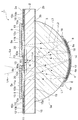
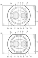
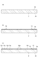
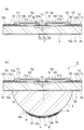
- FIG. 2 is a cross-sectional view taken along the line II-II in FIG. It is a bottom view of the spectroscopy module of FIG. It is sectional drawing for demonstrating the manufacturing method of the spectroscopy module of FIG. It is sectional drawing for demonstrating the manufacturing method of the spectroscopy module of FIG. It is sectional drawing for demonstrating the manufacturing method of the spectroscopy module of FIG. It is sectional drawing for demonstrating the manufacturing method of the spectroscopy module of FIG.
- the spectroscopic module 1 includes a substrate (main body portion, second portion) 2 and a lens portion (main body portion, first side) that transmit light Lm incident from the front side (one side). (Part) 3, the light Lm incident on the substrate 2 and the lens unit 3, and the spectroscopic unit (first spectroscopic unit) 4 that reflects the light Lm to the front side, and the light that is the ⁇ 1st order light split by the spectroscopic unit 4 And a light detection element (first light detection element) 5 for detecting L1 (first order first light) L1.
- the spectroscopic module 1 includes a reflecting unit 7 that reflects light (second light of the second order) L2 that is zero-order light split by the spectroscopic unit 4 to the rear side (the other side), and a reflecting unit.
- a light splitting unit 8 that splits the light L2 reflected by the light source 7 and reflects it to the front side, and a light detection element (second light detection element) 9 that detects the light (third light) L3 split by the light splitting unit 8. And.
- the substrate 2 is formed in a rectangular plate shape using light-transmitting glass such as BK7, Pyrex (registered trademark), quartz, light-transmitting molded glass, or light-transmitting plastic.
- a wiring 10 made of a single layer film such as Al or Au or a laminated film such as Cr—Pt—Au, Ti—Pt—Au, Ti—Ni—Au, or Cr—Au is formed on the front surface 2a of the substrate 2, a wiring 10 made of a single layer film such as Al or Au or a laminated film such as Cr—Pt—Au, Ti—Pt—Au, Ti—Ni—Au, or Cr—Au is formed.
- the wiring 10 includes a plurality of pad portions 10a, a plurality of pad portions 10b, and a plurality of connection portions 10c that connect the corresponding pad portions 10a and the pad portions 10b.
- a light absorption layer 12 is formed on the front surface 2 a of the substrate 2.
- the light absorption layer 12 exposes the pad portions 10 a and 10 b of the wiring 10, and covers the connection portion 10 c of the wiring 10.
- the light absorption layer 12 is provided with openings 12a, 12b, and 12c.
- the opening 12 b is located on one side in the longitudinal direction of the substrate 2, and the opening 12 c is located on the other side in the longitudinal direction of the substrate 2.
- the opening 12a is located between the opening 12b and the opening 12c.
- the opening 12a is a hole through which the light Lm incident on the substrate 2 and the lens unit 3 passes.
- the opening 12b is a hole through which the light L1 split by the spectroscopic unit 4 passes
- the opening 12c is a hole through which the light L3 split by the spectroscopic unit 8 passes.
- Materials for the light absorption layer 12 include black resist, colored resin (silicone, epoxy, acrylic, urethane, polyimide, composite resin, etc.) containing filler (carbon, oxide, etc.), metal such as Cr and Co, or oxidation Examples thereof include metals, laminated films thereof, porous ceramics, metals, and metal oxides.
- An insulating layer 11 is formed between the front surface 2 a of the substrate 2 and the light absorption layer 12.
- the insulating layer 11 exposes the pad portions 10 a and 10 b of the wiring 10 and covers the connection portion 10 c of the wiring 10.
- the insulating portion 11 a that is a part of the insulating layer 11 covers a portion on one side in the opening 12 b in the longitudinal direction of the substrate 2.
- the insulating part 11 b which is a part of the insulating layer 11 covers the other side part in the opening 12 c in the longitudinal direction of the substrate 2.
- the insulating portions 11a and 11b function as an optical filter that cuts light in a predetermined wavelength range.
- External terminals of rectangular plate-like photodetecting elements 5 and 9 are connected to the pad portion 10 a exposed from the insulating layer 11 and the light absorbing layer 12 by face-down bonding via bumps 13.
- the light detection element 5 is located on one side in the longitudinal direction of the substrate 2 so that the light detection portion 5a faces the opening 12b of the light absorption layer 12.
- the light detection element 9 is located on the other side in the longitudinal direction of the substrate 2 so that the light detection portion 9 a faces the opening 12 c of the light absorption layer 12.
- the photodetecting portion 5a of the photodetecting element 5 is constituted by a long photodiode arranged in a one-dimensional manner in a direction substantially perpendicular to the longitudinal direction.
- the photodetecting element 5 is arranged so that the one-dimensional arrangement direction of the photodiodes substantially coincides with the longitudinal direction of the substrate 2 and the photodetecting portion 5a faces the front surface 2a side of the substrate 2.
- the light detecting element 5 is not limited to a photodiode array, and may be a C-MOS image sensor, a CCD image sensor, or the like.
- the light detection element 5 is provided with a light passage hole 5b through which the light Lm incident on the substrate 2 and the lens unit 3 passes.
- the light passage hole 5b is arranged in parallel with the light detection part 5a along the one-dimensional arrangement direction of the photodiodes so as to face the opening part 12a of the light absorption layer 12.
- the light passage hole 5b is a slit extending in a direction substantially perpendicular to the longitudinal direction of the substrate 2 and substantially parallel to the front surface 2a of the substrate 2, and is etched while being positioned with high accuracy with respect to the light detection portion 5a. Etc. are formed.
- the light detection unit 9a of the light detection element 9 is composed of long photodiodes arranged one-dimensionally in a direction substantially perpendicular to the longitudinal direction. .
- the light detection element 9 is arranged so that the one-dimensional arrangement direction of the photodiodes substantially coincides with the longitudinal direction of the substrate 2 and the light detection portion 9a faces the front surface 2a side of the substrate 2.
- the light detection element 9 is not limited to a photodiode array, like the light detection element 5, and may be a C-MOS image sensor, a CCD image sensor, or the like.
- the substrate 2 side of the light detection element 5 (here, between the light detection element 5 and the substrate 2, the insulating layer 11 or the light absorption layer 12) is filled with an underfill material 20 that transmits at least the light L1. Yes.
- an underfill material 20 that transmits at least the light L3 is provided on the substrate 2 side of the light detection element 9 (here, between the light detection element 9 and the substrate 2, the insulating layer 11, or the light absorption layer 12). Filled.
- the underfill material 20 is filled entirely between the light detection elements 5 and 9 and the substrate 2, but the underfill material 20 is filled only around the bumps 13. It may be a configuration.
- the pad portion 10 b exposed from the insulating layer 11 and the light absorption layer 12 functions as an external terminal of the spectroscopic module 1. That is, external wiring or the like is electrically and physically connected to the pad portion 10b exposed from the light absorption layer 12.
- the rear surface 2b of the substrate 2 is provided with a lens portion 3 having a spherical outer surface 3a with the reflecting portion 7 interposed therebetween.
- the lens portion 3 is made of the same material as the substrate 2, a light-transmitting resin, a light-transmitting inorganic / organic hybrid material, or a light-transmitting low melting point glass for replica molding, plastic, etc.
- a side surface 3c is formed by cutting off two planes substantially orthogonal to 3b and substantially parallel to each other.
- the lens unit 3 is fitted into the opening 15a of the resist layer 15 formed on the rear surface 2b of the substrate 2, and is adhered to the rear surface 2b of the substrate 2 by an optical resin material 19 that transmits at least light Lm, L1, and L3. .
- the lens shape is not limited to a spherical lens, but may be an aspheric lens.
- the side surface 3c of the lens unit 3 may coincide with the side (outer edge) of the substrate 2 as shown in FIG. 3A, or as shown in FIG. You may be located inside 2 side (outer edge).
- the opening 15a of the resist layer 15 has a shape corresponding to the bottom surface (front surface) of the lens unit 3, thereby It is possible to prevent the lens unit 3 from moving in the rotation direction when the unit 3 is mounted and causing a shift in the mounting position of the lens unit 3.
- the spectroscopic parts 4 and 8 are provided on the rear side of the lens part 3.
- the spectroscopic unit 4 is located on one side in the longitudinal direction of the substrate 2 so as to face the light detection element 5.
- the spectroscopic unit 8 is located on the other side in the longitudinal direction of the substrate 2 so as to face the light detection element 9.
- the spectroscopic unit 4 includes a diffraction grating pattern 4a formed on the diffraction layer 6 and a reflection layer 17 formed so as to cover the diffraction grating pattern 4a.
- the spectroscopic unit 8 includes a diffraction grating pattern 8a formed on the diffraction layer 6 and a reflection layer 18 formed so as to cover the diffraction grating pattern 8a.
- the diffractive layer 6 is formed in a film shape along the outer surface 3 a of the lens unit 3, and the ridge part 16 is formed on the diffractive layer 6 along the peripheral edge 6 a so as to be thicker than the diffractive layer 6. It is integrally formed.
- the diffraction layer 6 and the flange portion 16 are provided by photocuring a replicating optical resin such as a photocurable epoxy resin, an acrylic resin, a fluorine resin, PMMA, silicone, or an organic-inorganic hybrid resin.
- the diffraction grating patterns 4 a and 8 a are, for example, a blazed grating having a sawtooth cross section, a binary grating having a rectangular cross section, a holographic grating having a sinusoidal cross section, and a plurality of grooves arranged in parallel in the longitudinal direction of the substrate 2. It is configured by being installed.
- the reflective layers 17 and 18 are film-like, and are formed by evaporating, for example, Al or Au.
- the diffraction layer 6 is formed in a circular shape when viewed from the rear side, and the flange portion 16 is formed in an annular shape when viewed from the rear side.
- Each of the reflection layers 17 and 18 is formed in a circular shape when viewed from the rear side, and is included in a region where the corresponding diffraction grating patterns 4a and 8a are formed.
- a protective layer 14 such as a passivation film is formed on the outer (rear) surface of the diffraction layer 6 so as to include and cover the reflective layers 17 and 18 when viewed from the rear side.
- the protective layer 14 has a film shape, and is formed of, for example, a vapor deposition film such as MgF 2 or SiO 2 , or an organic film having waterproofness and moisture resistance.
- the reflection unit 7 is located on the rear side (that is, the spectroscopic unit 4 and 8 side) with respect to the light detection unit 5a of the light detection element 5, the light detection unit 9a of the light detection element 9, and the light absorption layer 12. Further, the reflection part 7 faces the region R between the light detection part 5a and the light detection part 9a in the light absorption layer 12, and when viewed from the front side, the reflection part 7 and the light detection element 5 in the light absorption layer 12 A region R1 between the light detection element 9 (that is, a portion of the light absorption layer 12 exposed to the front side from between the light detection element 5 and the light detection element 9) is included.
- the light Lm incident on the substrate 2 and the lens unit 3 is split by the spectroscopic unit 4 and reflected to the front side.
- the light L ⁇ b> 1 travels forward and is detected by the light detection element 5.
- the light L ⁇ b> 2 travels forward and is reflected rearward by the reflecting unit 7.
- the light L2 reflected by the reflecting unit 7 is split by the spectroscopic unit 8 and reflected to the front side.
- the light L3 travels forward and is detected by the light detection element 9.
- the spectroscopic unit 8 and the photodetecting element 9 are provided, so that detection sensitivity can be increased with respect to light in a wide wavelength range or light in a different wavelength range. And the detectable wavelength range can be widened.
- a light passage hole 5b and a light absorption layer 12 are provided between the light detection part 5a of the light detection element 5 and the light detection part 9a of the light detection element 9, and the light absorption layer 12 (that is, the region R) is provided. ) Is provided so as to oppose. As described above, the spectral module 1 can be prevented from being enlarged by using the region between the light detection unit 5a and the light detection unit 9a.
- the spectroscopic characteristics in the lens unit 3 are part of the stray light. Unnecessary stray light increases. Since most of the light L2 has a light intensity that is not so high compared to the light L1, the light L3 that is the diffracted light of the light L2 has a further reduced light intensity. That is, the lights L2 and L3 are very susceptible to stray light caused by the disturbance light La. In order to alleviate such a situation, it is extremely effective to provide the reflecting portion 7 as described above.
- a region R ⁇ b> 1 provided between the light detection element 5 and the light detection element 9 is included in the reflection portion 7 when viewed from the front side of the substrate 2.
- region R1 can be reliably reflected by the area
- the diffractive layer 6 can be formed extremely thin so as to have a thickness of 1 ⁇ m to 20 ⁇ m. Thereby, the light absorption in the diffraction layer 6 can be suppressed and the light utilization efficiency can be improved. Moreover, by forming the diffractive layer 6 to be extremely thin, it is possible to suppress deformation (stretching and the like) of the diffractive layer 6 due to heat and moisture, and to ensure stable spectral characteristics and high reliability. It becomes.
- the flange portion 16 can be made thicker and more reliable than the diffractive layer 6, and the diffractive layer 6 can be peeled off from the outer surface 3a. It becomes possible to prevent.
- the substrate 2 is prepared. Thereafter, as shown in FIG. 4B, the wiring 10 is formed on the front surface 2 a of the substrate 2. Further, as shown in FIG. 4 (c), on the front surface 2a of the substrate 2, the portions to be the pad portions 10a and 10b of the wiring 10 are exposed to the front side, and the portions to be the connection portions 10c of the wiring 10 are covered. Thus, the insulating layer 11 is formed. When forming the insulating layer 11, the insulating portions 11 a and 11 b are simultaneously formed as part of the insulating layer 11. The insulating part 11a and the insulating part 11b may be formed of different materials and function as two types of optical filters.
- the front surface 2a of the substrate 2 is exposed to the front portions of the pad portions 10a and 10b and covers the portion of the connection portion 10c so as to cover the light absorption layer. 12 is formed.
- the reflecting portion 7 having a laminated structure including the base layer 7a, the intermediate layer 7b, and the reflecting layer 7c is formed on the rear surface 2b of the substrate 2 in this order from the rear surface 2b side.
- the base layer 7a is a Ti layer or a Cr layer
- the intermediate layer 7b is a Pt layer
- the reflective layer 7c is an Au layer.
- a resist layer 15 having an opening 15 a is formed on the rear surface 2 b of the substrate 2.
- the reflective layer 7c is not limited to the Au layer, and may be a layer made of a metal film such as Al or a metal oxide film having high reflectivity. Further, the reflection portion 7 may be formed by a dielectric multilayer mirror. These materials are selected with high reflectivity according to the wavelength handled by the spectroscopic module.
- the photodetecting element 5 is mounted on the pad portion 10 a of the wiring 10.
- the light detection element 9 is mounted on the pad portion 10a of the wiring 10 by face-down bonding via the bumps 13 so that the light detection portion 9a faces the opening 12c.
- the underfill material 20 is filled on the substrate 2 side of the light detection elements 5 and 9.
- the spectroscopic parts 4 and 8 are formed in the lens part 3. Specifically, a light transmissive master grating in which a grating corresponding to each of the diffraction grating patterns 4 a and 8 a is engraved is pressed against the replica optical resin dropped near the apex of the outer surface 3 a of the lens unit 3. Then, the optical resin for replica is cured by irradiating light in this state, and preferably, the diffractive layer 6 and the flange 16 are formed by performing heat curing in order to stabilize. Alternatively, a thermosetting resin may be used as the resin material, and the diffraction layer 6 or the like may be formed only by applying heat and pressure.
- the master grating is released, and Al, Au, or the like is deposited on the outer surface of the diffraction layer 6 by mask vapor deposition or entire vapor deposition, thereby forming the reflective layers 17 and 18 respectively.
- the protective layer 14 is formed by mask vapor deposition, full-surface vapor deposition, or resin coating of MgF 2 , SiO 2 or the like on the outer surfaces of the diffraction grating patterns 4 a and 8 a and the reflection layers 17 and 18.
- an optical resin material 19 is applied in the opening 15a of the resist layer 15 formed on the rear surface 2b of the substrate 2 to form the spectral portions 4 and 8.
- the lens unit 3 is bonded to the rear surface 2b of the substrate 2 so as to fit into the opening 15a.
- the optical resin material 19 is hardened by irradiating light, and the spectroscopy module 1 is obtained.
- the opening 15a of the resist layer 15 has a predetermined positional relationship with a pattern (not shown) on the substrate 2 that serves as a reference portion for positioning the photodetecting elements 5 and 9 on the substrate 2. It is formed by photoetching. At this time, since the spectroscopic units 4 and 8 are positioned with high accuracy with respect to the lens unit 3, the spectroscopic units 4 and 8 are positioned on the substrate 2 only by fitting the lens unit 3 into the opening 15a. . On the other hand, the light detection elements 5 and 9 are positioned on the substrate 2 by a pattern (not shown) on the substrate 2 which is a reference portion. Therefore, in addition to the spectroscopic unit 4 and the photodetecting element 5, alignment of the spectroscopic unit 8 and the photodetecting element 9 is realized only by fitting the lens unit 3 into the opening 15 a.
- the reflecting portion 7 is provided between the substrate 2 and the lens portion 3. According to this configuration, the reflecting portion 7 can be easily and accurately formed at a position facing the region R ⁇ b> 1 in the light absorption layer 12 on the spectroscopic portions 4 and 8 side with respect to the region R in the light absorption layer 12. Can do.
- the base layer 7 a is formed on the rear surface 2 b of the substrate 2, and the reflective layer 7 c is formed on the base layer 7 a, thereby providing the reflective portion 7 and sandwiching the reflective portion 7 between the substrate 2 and the lens portion. 3 is joined. Thereby, since the reflective layer 7c faces the spectroscopic units 4 and 8, the light L2 can be reliably reflected.
- the present invention is not limited to the embodiment described above.
- the reflecting portion 7 may be provided as a metal piece or the like embedded in the substrate 2 or the lens portion 3.
- a light passage hole may be provided in the region R ⁇ b> 1 in the light absorption layer 12 as a light incident part for allowing the light Lm to enter the substrate 2 and the lens part 3.
- the diffraction orders handled by the spectroscopic module are not limited to the light L1 being the ⁇ 1st order light and the light L2 being the 0th order light, but it is sufficient that the orders of the light L1 and the light L2 are different.
- a spectroscopic module that can accurately detect light in a wide wavelength range or light in different wavelength ranges while preventing an increase in size.
- SYMBOLS 1 ... Spectroscopic module, 2 ... Board
- Region area between the first light detection part and the second light detection part in the light absorption layer
- R1 Region (region between the first and second light detecting elements in the light absorption layer)
- Lm Location
- L1... Light first light
- L2. Light Light
- L3 Third light
Landscapes
- Physics & Mathematics (AREA)
- Spectroscopy & Molecular Physics (AREA)
- General Physics & Mathematics (AREA)
- Spectrometry And Color Measurement (AREA)
- Diffracting Gratings Or Hologram Optical Elements (AREA)
- Optical Elements Other Than Lenses (AREA)
- Investigating Or Analysing Materials By Optical Means (AREA)
Abstract
Description
Claims (3)
- 一方の側から入射した光を透過させる本体部と、
前記本体部の他方の側に設けられ、前記本体部に入射した光を分光すると共に前記本体部の一方の側に反射する第1の分光部と、
前記本体部の一方の側に配置され、前記第1の分光部によって分光された第1の次数の第1の光を検出する第1の光検出素子と、
前記第1の分光部によって分光された第2の次数の第2の光を反射する反射部と、
前記本体部の他方の側に設けられ、前記反射部によって反射された前記第2の光を分光すると共に前記本体部の一方の側に反射する第2の分光部と、
前記本体部の一方の側に配置され、前記第2の分光部によって分光された第3の光を検出する第2の光検出素子と、を備え、
前記本体部の一方の側において、前記第1の光検出素子の第1の光検出部と前記第2の光検出素子の第2の光検出部との間には、前記本体部に光を入射させる光入射部、及び光を吸収する光吸収層が設けられており、
前記反射部は、前記第1の光検出部及び前記第2の光検出部並びに前記光吸収層に対して前記第1の分光部及び前記第2の分光部側に位置し、前記光吸収層と対向していることを特徴とする分光モジュール。 - 前記光吸収層における前記第1の光検出素子と前記第2の光検出素子との間の領域は、前記本体部の一方の側から見た場合に前記反射部に含まれていることを特徴とする請求項1記載の分光モジュール。
- 前記本体部は、第1の部分と、前記第1の部分に対して前記第1の光検出素子及び前記第2の光検出素子側に位置し、前記第1の部分と接合された第2の部分と、を有し、
前記反射部は、前記第1の部分と前記第2の部分との間に設けられていることを特徴とする請求項1記載の分光モジュール。
Priority Applications (3)
| Application Number | Priority Date | Filing Date | Title |
|---|---|---|---|
| CN201180016678.3A CN102834702B (zh) | 2010-04-01 | 2011-03-16 | 分光模块 |
| US13/637,408 US9074933B2 (en) | 2010-04-01 | 2011-03-16 | Spectrometer module |
| DE112011101155.5T DE112011101155B4 (de) | 2010-04-01 | 2011-03-16 | Spektrometermodul |
Applications Claiming Priority (2)
| Application Number | Priority Date | Filing Date | Title |
|---|---|---|---|
| JP2010085206A JP5325829B2 (ja) | 2010-04-01 | 2010-04-01 | 分光モジュール |
| JP2010-085206 | 2010-04-01 |
Publications (1)
| Publication Number | Publication Date |
|---|---|
| WO2011125440A1 true WO2011125440A1 (ja) | 2011-10-13 |
Family
ID=44762400
Family Applications (1)
| Application Number | Title | Priority Date | Filing Date |
|---|---|---|---|
| PCT/JP2011/056247 Ceased WO2011125440A1 (ja) | 2010-04-01 | 2011-03-16 | 分光モジュール |
Country Status (5)
| Country | Link |
|---|---|
| US (1) | US9074933B2 (ja) |
| JP (1) | JP5325829B2 (ja) |
| CN (1) | CN102834702B (ja) |
| DE (1) | DE112011101155B4 (ja) |
| WO (1) | WO2011125440A1 (ja) |
Cited By (1)
| Publication number | Priority date | Publication date | Assignee | Title |
|---|---|---|---|---|
| WO2013079619A1 (en) * | 2011-12-01 | 2013-06-06 | Biosurfit, S.A. | Photometric device and method |
Families Citing this family (18)
| Publication number | Priority date | Publication date | Assignee | Title |
|---|---|---|---|---|
| WO2013065035A1 (en) | 2011-11-03 | 2013-05-10 | Verifood Ltd. | Low-cost spectrometry system for end-user food analysis |
| CN105593651B (zh) | 2013-08-02 | 2019-06-07 | 威利食品有限公司 | 光谱测定系统和方法、光谱设备和系统 |
| CN106461461A (zh) | 2014-01-03 | 2017-02-22 | 威利食品有限公司 | 光谱测定系统、方法和应用 |
| JP6325268B2 (ja) * | 2014-02-05 | 2018-05-16 | 浜松ホトニクス株式会社 | 分光器、及び分光器の製造方法 |
| JP6251073B2 (ja) * | 2014-02-05 | 2017-12-20 | 浜松ホトニクス株式会社 | 分光器、及び分光器の製造方法 |
| DE102014211240A1 (de) * | 2014-06-12 | 2015-12-17 | Carl Zeiss Microscopy Gmbh | Spektrometrisches Messinstrument und Verfahren zur Kopplung spektrometrischer Messinstrumente |
| CN107250739A (zh) | 2014-10-23 | 2017-10-13 | 威利食品有限公司 | 手持式光谱仪的附件 |
| WO2016125165A2 (en) | 2015-02-05 | 2016-08-11 | Verifood, Ltd. | Spectrometry system with visible aiming beam |
| WO2016125164A2 (en) | 2015-02-05 | 2016-08-11 | Verifood, Ltd. | Spectrometry system applications |
| WO2016162865A1 (en) | 2015-04-07 | 2016-10-13 | Verifood, Ltd. | Detector for spectrometry system |
| US10066990B2 (en) | 2015-07-09 | 2018-09-04 | Verifood, Ltd. | Spatially variable filter systems and methods |
| US10203246B2 (en) | 2015-11-20 | 2019-02-12 | Verifood, Ltd. | Systems and methods for calibration of a handheld spectrometer |
| US10254215B2 (en) | 2016-04-07 | 2019-04-09 | Verifood, Ltd. | Spectrometry system applications |
| WO2018015951A1 (en) | 2016-07-20 | 2018-01-25 | Verifood, Ltd. | Accessories for handheld spectrometer |
| US10791933B2 (en) | 2016-07-27 | 2020-10-06 | Verifood, Ltd. | Spectrometry systems, methods, and applications |
| EP3372966B1 (en) * | 2017-03-10 | 2021-09-01 | Hitachi High-Tech Analytical Science Limited | A portable analyzer using optical emission spectoscopy |
| EP3864384A4 (en) | 2018-10-08 | 2022-06-29 | Verifood Ltd. | Accessories for optical spectrometers |
| CN114124212A (zh) * | 2020-08-26 | 2022-03-01 | 华为技术有限公司 | 一种分光探测器及光纤通信系统 |
Citations (5)
| Publication number | Priority date | Publication date | Assignee | Title |
|---|---|---|---|---|
| JPH0339572B2 (ja) * | 1982-01-04 | 1991-06-14 | Instruments Sa | |
| JP2000171300A (ja) * | 1998-11-21 | 2000-06-23 | Sai G Fuer Analytische Messgeraete Mbh | 半導体ラインセンサ又は光電子倍増器を備えた二重格子―同時分光計 |
| DE10137428A1 (de) * | 2001-07-27 | 2003-02-20 | Karlsruhe Forschzent | Vorrichtung zur Messung eines Spektrums |
| JP2009092680A (ja) * | 2007-10-03 | 2009-04-30 | Yokogawa Electric Corp | 回折格子及びこれを用いた分光装置 |
| JP2009300424A (ja) * | 2008-05-15 | 2009-12-24 | Hamamatsu Photonics Kk | 分光モジュール及び分光モジュールの製造方法 |
Family Cites Families (12)
| Publication number | Priority date | Publication date | Assignee | Title |
|---|---|---|---|---|
| JP2662816B2 (ja) | 1989-07-07 | 1997-10-15 | 富士変速機株式会社 | 地下式立体駐車装置 |
| DE4038638A1 (de) | 1990-12-04 | 1992-06-11 | Zeiss Carl Fa | Diodenzeilen-spektrometer |
| FR2689349B1 (fr) | 1992-03-31 | 1994-05-06 | Alcatel Nv | Multiplexeur en longueur d'onde pour systeme optique integre. |
| WO2003069291A1 (en) | 2002-02-14 | 2003-08-21 | Containerless Research, Inc. | Photopolarimeters and spectrophotopolarimaters with multiple diffraction gratings |
| US7733492B1 (en) | 2004-06-04 | 2010-06-08 | University Of Hawaii | Sagnac fourier transform spectrometer having improved resolution |
| DE102004028001A1 (de) | 2004-06-09 | 2006-01-05 | Gesellschaft zur Förderung angewandter Optik, Optoelektronik, Quantenelektronik und Spektroskopie e.V. | Echelle-Spektrometer mit verbesserter Detektorausnutzung |
| DE102006017705B4 (de) * | 2006-04-15 | 2010-01-07 | Carl Zeiss Microimaging Gmbh | Spektralanalytische Einheit mit einem Beugungsgitter und Laserscanning-Mikroskop |
| WO2008149940A1 (ja) | 2007-06-08 | 2008-12-11 | Hamamatsu Photonics K.K. | 分光モジュール |
| CN100545697C (zh) | 2007-12-29 | 2009-09-30 | 苏州大学 | 微型超光谱成像系统 |
| JP5205242B2 (ja) | 2008-05-15 | 2013-06-05 | 浜松ホトニクス株式会社 | 分光器の製造方法 |
| JP5205239B2 (ja) | 2008-05-15 | 2013-06-05 | 浜松ホトニクス株式会社 | 分光器 |
| JP2009300418A (ja) | 2008-05-15 | 2009-12-24 | Hamamatsu Photonics Kk | 分光モジュール |
-
2010
- 2010-04-01 JP JP2010085206A patent/JP5325829B2/ja active Active
-
2011
- 2011-03-16 DE DE112011101155.5T patent/DE112011101155B4/de active Active
- 2011-03-16 US US13/637,408 patent/US9074933B2/en active Active
- 2011-03-16 CN CN201180016678.3A patent/CN102834702B/zh active Active
- 2011-03-16 WO PCT/JP2011/056247 patent/WO2011125440A1/ja not_active Ceased
Patent Citations (5)
| Publication number | Priority date | Publication date | Assignee | Title |
|---|---|---|---|---|
| JPH0339572B2 (ja) * | 1982-01-04 | 1991-06-14 | Instruments Sa | |
| JP2000171300A (ja) * | 1998-11-21 | 2000-06-23 | Sai G Fuer Analytische Messgeraete Mbh | 半導体ラインセンサ又は光電子倍増器を備えた二重格子―同時分光計 |
| DE10137428A1 (de) * | 2001-07-27 | 2003-02-20 | Karlsruhe Forschzent | Vorrichtung zur Messung eines Spektrums |
| JP2009092680A (ja) * | 2007-10-03 | 2009-04-30 | Yokogawa Electric Corp | 回折格子及びこれを用いた分光装置 |
| JP2009300424A (ja) * | 2008-05-15 | 2009-12-24 | Hamamatsu Photonics Kk | 分光モジュール及び分光モジュールの製造方法 |
Cited By (2)
| Publication number | Priority date | Publication date | Assignee | Title |
|---|---|---|---|---|
| WO2013079619A1 (en) * | 2011-12-01 | 2013-06-06 | Biosurfit, S.A. | Photometric device and method |
| US9594016B2 (en) | 2011-12-01 | 2017-03-14 | Biosurfit, S.A. | Photometric device and method |
Also Published As
| Publication number | Publication date |
|---|---|
| DE112011101155T5 (de) | 2013-01-10 |
| CN102834702A (zh) | 2012-12-19 |
| CN102834702B (zh) | 2015-04-08 |
| JP2011215075A (ja) | 2011-10-27 |
| JP5325829B2 (ja) | 2013-10-23 |
| DE112011101155B4 (de) | 2021-08-26 |
| US20130141718A1 (en) | 2013-06-06 |
| US9074933B2 (en) | 2015-07-07 |
Similar Documents
| Publication | Publication Date | Title |
|---|---|---|
| JP5325829B2 (ja) | 分光モジュール | |
| CN102822647B (zh) | 分光模块 | |
| JP4891840B2 (ja) | 分光モジュール | |
| JP4887221B2 (ja) | 分光モジュール | |
| JP5592089B2 (ja) | 分光モジュール及びその製造方法 | |
| JP5205241B2 (ja) | 分光モジュール | |
| JP4887251B2 (ja) | 分光モジュール | |
| WO2011027747A1 (ja) | 分光モジュール | |
| JP4887250B2 (ja) | 分光モジュール | |
| JP5799145B2 (ja) | 分光部及びその製造方法 | |
| JP5113947B2 (ja) | 分光モジュール | |
| JP4980184B2 (ja) | 分光モジュール | |
| JP5097294B2 (ja) | 分光モジュール | |
| JP4966428B2 (ja) | 分光モジュール | |
| JP2013007707A (ja) | 分光モジュール |
Legal Events
| Date | Code | Title | Description |
|---|---|---|---|
| WWE | Wipo information: entry into national phase |
Ref document number: 201180016678.3 Country of ref document: CN |
|
| 121 | Ep: the epo has been informed by wipo that ep was designated in this application |
Ref document number: 11765342 Country of ref document: EP Kind code of ref document: A1 |
|
| WWE | Wipo information: entry into national phase |
Ref document number: 1120111011555 Country of ref document: DE Ref document number: 112011101155 Country of ref document: DE |
|
| WWE | Wipo information: entry into national phase |
Ref document number: 13637408 Country of ref document: US |
|
| 122 | Ep: pct application non-entry in european phase |
Ref document number: 11765342 Country of ref document: EP Kind code of ref document: A1 |