WO2011125363A1 - 有機el素子、有機elディスプレイおよび有機el表示装置 - Google Patents
有機el素子、有機elディスプレイおよび有機el表示装置 Download PDFInfo
- Publication number
- WO2011125363A1 WO2011125363A1 PCT/JP2011/051650 JP2011051650W WO2011125363A1 WO 2011125363 A1 WO2011125363 A1 WO 2011125363A1 JP 2011051650 W JP2011051650 W JP 2011051650W WO 2011125363 A1 WO2011125363 A1 WO 2011125363A1
- Authority
- WO
- WIPO (PCT)
- Prior art keywords
- organic
- layer
- light
- phosphor layer
- distribution characteristic
- Prior art date
Links
- 238000005401 electroluminescence Methods 0.000 title abstract description 13
- OAICVXFJPJFONN-UHFFFAOYSA-N Phosphorus Chemical compound [P] OAICVXFJPJFONN-UHFFFAOYSA-N 0.000 claims abstract description 286
- 238000009826 distribution Methods 0.000 claims abstract description 150
- 230000000694 effects Effects 0.000 claims abstract description 25
- 239000000463 material Substances 0.000 claims description 145
- 238000000034 method Methods 0.000 claims description 132
- 239000002245 particle Substances 0.000 claims description 96
- 238000000149 argon plasma sintering Methods 0.000 claims description 42
- 229910010272 inorganic material Inorganic materials 0.000 claims description 30
- 239000011147 inorganic material Substances 0.000 claims description 29
- 239000004973 liquid crystal related substance Substances 0.000 claims description 27
- 239000011159 matrix material Substances 0.000 claims description 10
- 229910052709 silver Inorganic materials 0.000 claims description 9
- 239000004332 silver Substances 0.000 claims description 9
- 238000013459 approach Methods 0.000 claims description 5
- 239000010410 layer Substances 0.000 description 507
- 239000000758 substrate Substances 0.000 description 153
- 239000010408 film Substances 0.000 description 141
- 238000007789 sealing Methods 0.000 description 66
- 239000007924 injection Substances 0.000 description 53
- 238000002347 injection Methods 0.000 description 53
- 229920005989 resin Polymers 0.000 description 49
- 239000011347 resin Substances 0.000 description 49
- 230000008859 change Effects 0.000 description 29
- 238000000576 coating method Methods 0.000 description 26
- -1 polyethylene terephthalate Polymers 0.000 description 26
- 239000011248 coating agent Substances 0.000 description 22
- 230000005525 hole transport Effects 0.000 description 19
- 230000001965 increasing effect Effects 0.000 description 18
- 229910052751 metal Inorganic materials 0.000 description 18
- 239000002184 metal Substances 0.000 description 18
- 230000008569 process Effects 0.000 description 18
- 238000007740 vapor deposition Methods 0.000 description 18
- 239000011324 bead Substances 0.000 description 17
- 150000001875 compounds Chemical class 0.000 description 16
- 238000010438 heat treatment Methods 0.000 description 15
- 230000003287 optical effect Effects 0.000 description 13
- VYPSYNLAJGMNEJ-UHFFFAOYSA-N silicon dioxide Inorganic materials O=[Si]=O VYPSYNLAJGMNEJ-UHFFFAOYSA-N 0.000 description 13
- 239000011368 organic material Substances 0.000 description 12
- 239000004065 semiconductor Substances 0.000 description 12
- 229910052581 Si3N4 Inorganic materials 0.000 description 11
- 229910004283 SiO 4 Inorganic materials 0.000 description 11
- 230000000052 comparative effect Effects 0.000 description 11
- 230000007423 decrease Effects 0.000 description 11
- 229910052757 nitrogen Inorganic materials 0.000 description 11
- 229910021420 polycrystalline silicon Inorganic materials 0.000 description 11
- HQVNEWCFYHHQES-UHFFFAOYSA-N silicon nitride Chemical compound N12[Si]34N5[Si]62N3[Si]51N64 HQVNEWCFYHHQES-UHFFFAOYSA-N 0.000 description 11
- 239000000126 substance Substances 0.000 description 11
- 239000011521 glass Substances 0.000 description 10
- 230000002265 prevention Effects 0.000 description 10
- 239000000243 solution Substances 0.000 description 10
- 238000004544 sputter deposition Methods 0.000 description 10
- 229910004298 SiO 2 Inorganic materials 0.000 description 9
- 239000007788 liquid Substances 0.000 description 9
- 238000005192 partition Methods 0.000 description 9
- 238000000206 photolithography Methods 0.000 description 9
- 239000002861 polymer material Substances 0.000 description 9
- BQCADISMDOOEFD-UHFFFAOYSA-N Silver Chemical compound [Ag] BQCADISMDOOEFD-UHFFFAOYSA-N 0.000 description 8
- 229910021417 amorphous silicon Inorganic materials 0.000 description 8
- 239000000470 constituent Substances 0.000 description 8
- 239000002019 doping agent Substances 0.000 description 8
- 239000000975 dye Substances 0.000 description 8
- LIVNPJMFVYWSIS-UHFFFAOYSA-N silicon monoxide Chemical compound [Si-]#[O+] LIVNPJMFVYWSIS-UHFFFAOYSA-N 0.000 description 8
- XLYOFNOQVPJJNP-UHFFFAOYSA-N water Substances O XLYOFNOQVPJJNP-UHFFFAOYSA-N 0.000 description 8
- 230000015572 biosynthetic process Effects 0.000 description 7
- 238000000295 emission spectrum Methods 0.000 description 7
- 239000000203 mixture Substances 0.000 description 7
- 229920003023 plastic Polymers 0.000 description 7
- 239000004033 plastic Substances 0.000 description 7
- 239000004925 Acrylic resin Substances 0.000 description 6
- 229920000178 Acrylic resin Polymers 0.000 description 6
- IAZDPXIOMUYVGZ-UHFFFAOYSA-N Dimethylsulphoxide Chemical compound CS(C)=O IAZDPXIOMUYVGZ-UHFFFAOYSA-N 0.000 description 6
- 108010043121 Green Fluorescent Proteins Proteins 0.000 description 6
- XLOMVQKBTHCTTD-UHFFFAOYSA-N Zinc monoxide Chemical compound [Zn]=O XLOMVQKBTHCTTD-UHFFFAOYSA-N 0.000 description 6
- 229910052782 aluminium Inorganic materials 0.000 description 6
- XAGFODPZIPBFFR-UHFFFAOYSA-N aluminium Chemical compound [Al] XAGFODPZIPBFFR-UHFFFAOYSA-N 0.000 description 6
- ZYGHJZDHTFUPRJ-UHFFFAOYSA-N coumarin Chemical compound C1=CC=C2OC(=O)C=CC2=C1 ZYGHJZDHTFUPRJ-UHFFFAOYSA-N 0.000 description 6
- 238000010894 electron beam technology Methods 0.000 description 6
- 239000010931 gold Substances 0.000 description 6
- 239000011810 insulating material Substances 0.000 description 6
- 238000004519 manufacturing process Methods 0.000 description 6
- 230000004048 modification Effects 0.000 description 6
- 238000012986 modification Methods 0.000 description 6
- BASFCYQUMIYNBI-UHFFFAOYSA-N platinum Chemical compound [Pt] BASFCYQUMIYNBI-UHFFFAOYSA-N 0.000 description 6
- 229920005591 polysilicon Polymers 0.000 description 6
- 238000007639 printing Methods 0.000 description 6
- 229920000877 Melamine resin Polymers 0.000 description 5
- 239000003086 colorant Substances 0.000 description 5
- 230000007547 defect Effects 0.000 description 5
- 238000000151 deposition Methods 0.000 description 5
- 238000001035 drying Methods 0.000 description 5
- 230000005284 excitation Effects 0.000 description 5
- 239000010419 fine particle Substances 0.000 description 5
- 229910052738 indium Inorganic materials 0.000 description 5
- APFVFJFRJDLVQX-UHFFFAOYSA-N indium atom Chemical compound [In] APFVFJFRJDLVQX-UHFFFAOYSA-N 0.000 description 5
- 238000004518 low pressure chemical vapour deposition Methods 0.000 description 5
- 238000007650 screen-printing Methods 0.000 description 5
- 238000004528 spin coating Methods 0.000 description 5
- 229920001187 thermosetting polymer Polymers 0.000 description 5
- CSCPPACGZOOCGX-UHFFFAOYSA-N Acetone Chemical compound CC(C)=O CSCPPACGZOOCGX-UHFFFAOYSA-N 0.000 description 4
- LFQSCWFLJHTTHZ-UHFFFAOYSA-N Ethanol Chemical compound CCO LFQSCWFLJHTTHZ-UHFFFAOYSA-N 0.000 description 4
- JUJWROOIHBZHMG-UHFFFAOYSA-N Pyridine Chemical compound C1=CC=NC=C1 JUJWROOIHBZHMG-UHFFFAOYSA-N 0.000 description 4
- 239000007983 Tris buffer Substances 0.000 description 4
- 239000000654 additive Substances 0.000 description 4
- 238000006243 chemical reaction Methods 0.000 description 4
- 238000005229 chemical vapour deposition Methods 0.000 description 4
- 239000010949 copper Substances 0.000 description 4
- 230000008021 deposition Effects 0.000 description 4
- 238000010586 diagram Methods 0.000 description 4
- 239000007789 gas Substances 0.000 description 4
- PCHJSUWPFVWCPO-UHFFFAOYSA-N gold Chemical compound [Au] PCHJSUWPFVWCPO-UHFFFAOYSA-N 0.000 description 4
- 229910052737 gold Inorganic materials 0.000 description 4
- MRELNEQAGSRDBK-UHFFFAOYSA-N lanthanum(3+);oxygen(2-) Chemical compound [O-2].[O-2].[O-2].[La+3].[La+3] MRELNEQAGSRDBK-UHFFFAOYSA-N 0.000 description 4
- 239000011777 magnesium Substances 0.000 description 4
- 229920000553 poly(phenylenevinylene) Polymers 0.000 description 4
- 238000012545 processing Methods 0.000 description 4
- 238000002834 transmittance Methods 0.000 description 4
- ZOKIJILZFXPFTO-UHFFFAOYSA-N 4-methyl-n-[4-[1-[4-(4-methyl-n-(4-methylphenyl)anilino)phenyl]cyclohexyl]phenyl]-n-(4-methylphenyl)aniline Chemical compound C1=CC(C)=CC=C1N(C=1C=CC(=CC=1)C1(CCCCC1)C=1C=CC(=CC=1)N(C=1C=CC(C)=CC=1)C=1C=CC(C)=CC=1)C1=CC=C(C)C=C1 ZOKIJILZFXPFTO-UHFFFAOYSA-N 0.000 description 3
- UJOBWOGCFQCDNV-UHFFFAOYSA-N Carbazole Natural products C1=CC=C2C3=CC=CC=C3NC2=C1 UJOBWOGCFQCDNV-UHFFFAOYSA-N 0.000 description 3
- KFZMGEQAYNKOFK-UHFFFAOYSA-N Isopropanol Chemical compound CC(C)O KFZMGEQAYNKOFK-UHFFFAOYSA-N 0.000 description 3
- PXHVJJICTQNCMI-UHFFFAOYSA-N Nickel Chemical compound [Ni] PXHVJJICTQNCMI-UHFFFAOYSA-N 0.000 description 3
- 239000004642 Polyimide Substances 0.000 description 3
- 239000004793 Polystyrene Substances 0.000 description 3
- 239000004372 Polyvinyl alcohol Substances 0.000 description 3
- PPBRXRYQALVLMV-UHFFFAOYSA-N Styrene Natural products C=CC1=CC=CC=C1 PPBRXRYQALVLMV-UHFFFAOYSA-N 0.000 description 3
- ATJFFYVFTNAWJD-UHFFFAOYSA-N Tin Chemical compound [Sn] ATJFFYVFTNAWJD-UHFFFAOYSA-N 0.000 description 3
- GWEVSGVZZGPLCZ-UHFFFAOYSA-N Titan oxide Chemical compound O=[Ti]=O GWEVSGVZZGPLCZ-UHFFFAOYSA-N 0.000 description 3
- 238000010521 absorption reaction Methods 0.000 description 3
- 150000001448 anilines Chemical class 0.000 description 3
- XKHYPFFZHSGMBE-UHFFFAOYSA-N buta-1,3-diene-1,1,2,3,4,4-hexacarbonitrile Chemical compound N#CC(C#N)=C(C#N)C(C#N)=C(C#N)C#N XKHYPFFZHSGMBE-UHFFFAOYSA-N 0.000 description 3
- 239000003990 capacitor Substances 0.000 description 3
- 230000015556 catabolic process Effects 0.000 description 3
- 239000000460 chlorine Substances 0.000 description 3
- 238000004140 cleaning Methods 0.000 description 3
- 238000007796 conventional method Methods 0.000 description 3
- 229960000956 coumarin Drugs 0.000 description 3
- 235000001671 coumarin Nutrition 0.000 description 3
- 125000004093 cyano group Chemical group *C#N 0.000 description 3
- 230000006866 deterioration Effects 0.000 description 3
- 230000006872 improvement Effects 0.000 description 3
- 239000011229 interlayer Substances 0.000 description 3
- 238000007733 ion plating Methods 0.000 description 3
- 150000002500 ions Chemical class 0.000 description 3
- 238000003475 lamination Methods 0.000 description 3
- JDSHMPZPIAZGSV-UHFFFAOYSA-N melamine Chemical compound NC1=NC(N)=NC(N)=N1 JDSHMPZPIAZGSV-UHFFFAOYSA-N 0.000 description 3
- 239000011259 mixed solution Substances 0.000 description 3
- 238000002156 mixing Methods 0.000 description 3
- 239000012044 organic layer Substances 0.000 description 3
- 230000003647 oxidation Effects 0.000 description 3
- 238000007254 oxidation reaction Methods 0.000 description 3
- 229920001721 polyimide Polymers 0.000 description 3
- 229920000642 polymer Polymers 0.000 description 3
- 229920002223 polystyrene Polymers 0.000 description 3
- 229920002451 polyvinyl alcohol Polymers 0.000 description 3
- 229910052814 silicon oxide Inorganic materials 0.000 description 3
- NLDYACGHTUPAQU-UHFFFAOYSA-N tetracyanoethylene Chemical compound N#CC(C#N)=C(C#N)C#N NLDYACGHTUPAQU-UHFFFAOYSA-N 0.000 description 3
- 229910052718 tin Inorganic materials 0.000 description 3
- 238000004506 ultrasonic cleaning Methods 0.000 description 3
- 238000001771 vacuum deposition Methods 0.000 description 3
- 239000011787 zinc oxide Substances 0.000 description 3
- QGKMIGUHVLGJBR-UHFFFAOYSA-M (4z)-1-(3-methylbutyl)-4-[[1-(3-methylbutyl)quinolin-1-ium-4-yl]methylidene]quinoline;iodide Chemical compound [I-].C12=CC=CC=C2N(CCC(C)C)C=CC1=CC1=CC=[N+](CCC(C)C)C2=CC=CC=C12 QGKMIGUHVLGJBR-UHFFFAOYSA-M 0.000 description 2
- ZXBSSAFKXWFUMF-UHFFFAOYSA-N 1,2,3-trinitrofluoren-9-one Chemical compound C12=CC=CC=C2C(=O)C2=C1C=C([N+](=O)[O-])C([N+]([O-])=O)=C2[N+]([O-])=O ZXBSSAFKXWFUMF-UHFFFAOYSA-N 0.000 description 2
- UHXOHPVVEHBKKT-UHFFFAOYSA-N 1-(2,2-diphenylethenyl)-4-[4-(2,2-diphenylethenyl)phenyl]benzene Chemical group C=1C=C(C=2C=CC(C=C(C=3C=CC=CC=3)C=3C=CC=CC=3)=CC=2)C=CC=1C=C(C=1C=CC=CC=1)C1=CC=CC=C1 UHXOHPVVEHBKKT-UHFFFAOYSA-N 0.000 description 2
- JWWQNDLIYXEFQL-UHFFFAOYSA-N 2,3-dinitrofluoren-1-one Chemical compound C1=CC=C2C3=CC([N+](=O)[O-])=C([N+]([O-])=O)C(=O)C3=CC2=C1 JWWQNDLIYXEFQL-UHFFFAOYSA-N 0.000 description 2
- OGGKVJMNFFSDEV-UHFFFAOYSA-N 3-methyl-n-[4-[4-(n-(3-methylphenyl)anilino)phenyl]phenyl]-n-phenylaniline Chemical compound CC1=CC=CC(N(C=2C=CC=CC=2)C=2C=CC(=CC=2)C=2C=CC(=CC=2)N(C=2C=CC=CC=2)C=2C=C(C)C=CC=2)=C1 OGGKVJMNFFSDEV-UHFFFAOYSA-N 0.000 description 2
- MBPCKEZNJVJYTC-UHFFFAOYSA-N 4-[4-(n-phenylanilino)phenyl]aniline Chemical compound C1=CC(N)=CC=C1C1=CC=C(N(C=2C=CC=CC=2)C=2C=CC=CC=2)C=C1 MBPCKEZNJVJYTC-UHFFFAOYSA-N 0.000 description 2
- QPQKUYVSJWQSDY-UHFFFAOYSA-N 4-phenyldiazenylaniline Chemical compound C1=CC(N)=CC=C1N=NC1=CC=CC=C1 QPQKUYVSJWQSDY-UHFFFAOYSA-N 0.000 description 2
- 229910002012 Aerosil® Inorganic materials 0.000 description 2
- XKRFYHLGVUSROY-UHFFFAOYSA-N Argon Chemical compound [Ar] XKRFYHLGVUSROY-UHFFFAOYSA-N 0.000 description 2
- NLZUEZXRPGMBCV-UHFFFAOYSA-N Butylhydroxytoluene Chemical compound CC1=CC(C(C)(C)C)=C(O)C(C(C)(C)C)=C1 NLZUEZXRPGMBCV-UHFFFAOYSA-N 0.000 description 2
- RYGMFSIKBFXOCR-UHFFFAOYSA-N Copper Chemical compound [Cu] RYGMFSIKBFXOCR-UHFFFAOYSA-N 0.000 description 2
- FYYHWMGAXLPEAU-UHFFFAOYSA-N Magnesium Chemical compound [Mg] FYYHWMGAXLPEAU-UHFFFAOYSA-N 0.000 description 2
- 229920001609 Poly(3,4-ethylenedioxythiophene) Polymers 0.000 description 2
- XUIMIQQOPSSXEZ-UHFFFAOYSA-N Silicon Chemical compound [Si] XUIMIQQOPSSXEZ-UHFFFAOYSA-N 0.000 description 2
- YTPLMLYBLZKORZ-UHFFFAOYSA-N Thiophene Chemical compound C=1C=CSC=1 YTPLMLYBLZKORZ-UHFFFAOYSA-N 0.000 description 2
- MCMNRKCIXSYSNV-UHFFFAOYSA-N Zirconium dioxide Chemical compound O=[Zr]=O MCMNRKCIXSYSNV-UHFFFAOYSA-N 0.000 description 2
- NIXOWILDQLNWCW-UHFFFAOYSA-N acrylic acid group Chemical group C(C=C)(=O)O NIXOWILDQLNWCW-UHFFFAOYSA-N 0.000 description 2
- 230000000996 additive effect Effects 0.000 description 2
- 229910052783 alkali metal Inorganic materials 0.000 description 2
- 150000001340 alkali metals Chemical class 0.000 description 2
- PNEYBMLMFCGWSK-UHFFFAOYSA-N aluminium oxide Inorganic materials [O-2].[O-2].[O-2].[Al+3].[Al+3] PNEYBMLMFCGWSK-UHFFFAOYSA-N 0.000 description 2
- MWPLVEDNUUSJAV-UHFFFAOYSA-N anthracene Chemical compound C1=CC=CC2=CC3=CC=CC=C3C=C21 MWPLVEDNUUSJAV-UHFFFAOYSA-N 0.000 description 2
- 125000003118 aryl group Chemical group 0.000 description 2
- QVQLCTNNEUAWMS-UHFFFAOYSA-N barium oxide Chemical compound [Ba]=O QVQLCTNNEUAWMS-UHFFFAOYSA-N 0.000 description 2
- XJHABGPPCLHLLV-UHFFFAOYSA-N benzo[de]isoquinoline-1,3-dione Chemical compound C1=CC(C(=O)NC2=O)=C3C2=CC=CC3=C1 XJHABGPPCLHLLV-UHFFFAOYSA-N 0.000 description 2
- 230000000903 blocking effect Effects 0.000 description 2
- 150000001716 carbazoles Chemical class 0.000 description 2
- 229910052802 copper Inorganic materials 0.000 description 2
- 230000003247 decreasing effect Effects 0.000 description 2
- 238000006731 degradation reaction Methods 0.000 description 2
- TXCDCPKCNAJMEE-UHFFFAOYSA-N dibenzofuran Chemical compound C1=CC=C2C3=CC=CC=C3OC2=C1 TXCDCPKCNAJMEE-UHFFFAOYSA-N 0.000 description 2
- QXYJCZRRLLQGCR-UHFFFAOYSA-N dioxomolybdenum Chemical compound O=[Mo]=O QXYJCZRRLLQGCR-UHFFFAOYSA-N 0.000 description 2
- 238000007598 dipping method Methods 0.000 description 2
- GNTDGMZSJNCJKK-UHFFFAOYSA-N divanadium pentaoxide Chemical compound O=[V](=O)O[V](=O)=O GNTDGMZSJNCJKK-UHFFFAOYSA-N 0.000 description 2
- 238000007606 doctor blade method Methods 0.000 description 2
- 239000007772 electrode material Substances 0.000 description 2
- NIHNNTQXNPWCJQ-UHFFFAOYSA-N fluorene Chemical compound C1=CC=C2CC3=CC=CC=C3C2=C1 NIHNNTQXNPWCJQ-UHFFFAOYSA-N 0.000 description 2
- 150000002220 fluorenes Chemical class 0.000 description 2
- 150000008376 fluorenones Chemical class 0.000 description 2
- 239000007850 fluorescent dye Substances 0.000 description 2
- 238000007756 gravure coating Methods 0.000 description 2
- 238000004770 highest occupied molecular orbital Methods 0.000 description 2
- 239000012535 impurity Substances 0.000 description 2
- 239000011261 inert gas Substances 0.000 description 2
- 229910052741 iridium Inorganic materials 0.000 description 2
- GKOZUEZYRPOHIO-UHFFFAOYSA-N iridium atom Chemical compound [Ir] GKOZUEZYRPOHIO-UHFFFAOYSA-N 0.000 description 2
- AOZVYCYMTUWJHJ-UHFFFAOYSA-K iridium(3+) pyridine-2-carboxylate Chemical compound [Ir+3].[O-]C(=O)C1=CC=CC=N1.[O-]C(=O)C1=CC=CC=N1.[O-]C(=O)C1=CC=CC=N1 AOZVYCYMTUWJHJ-UHFFFAOYSA-K 0.000 description 2
- 238000010030 laminating Methods 0.000 description 2
- PQXKHYXIUOZZFA-UHFFFAOYSA-M lithium fluoride Chemical compound [Li+].[F-] PQXKHYXIUOZZFA-UHFFFAOYSA-M 0.000 description 2
- 238000004768 lowest unoccupied molecular orbital Methods 0.000 description 2
- 229910052749 magnesium Inorganic materials 0.000 description 2
- 150000002739 metals Chemical class 0.000 description 2
- 238000001451 molecular beam epitaxy Methods 0.000 description 2
- 239000004570 mortar (masonry) Substances 0.000 description 2
- 125000000449 nitro group Chemical group [O-][N+](*)=O 0.000 description 2
- 150000004866 oxadiazoles Chemical class 0.000 description 2
- BPUBBGLMJRNUCC-UHFFFAOYSA-N oxygen(2-);tantalum(5+) Chemical compound [O-2].[O-2].[O-2].[O-2].[O-2].[Ta+5].[Ta+5] BPUBBGLMJRNUCC-UHFFFAOYSA-N 0.000 description 2
- 238000000059 patterning Methods 0.000 description 2
- SLIUAWYAILUBJU-UHFFFAOYSA-N pentacene Chemical compound C1=CC=CC2=CC3=CC4=CC5=CC=CC=C5C=C4C=C3C=C21 SLIUAWYAILUBJU-UHFFFAOYSA-N 0.000 description 2
- 239000012466 permeate Substances 0.000 description 2
- YNPNZTXNASCQKK-UHFFFAOYSA-N phenanthrene Chemical compound C1=CC=C2C3=CC=CC=C3C=CC2=C1 YNPNZTXNASCQKK-UHFFFAOYSA-N 0.000 description 2
- 229910052698 phosphorus Inorganic materials 0.000 description 2
- XHXFXVLFKHQFAL-UHFFFAOYSA-N phosphoryl trichloride Chemical compound ClP(Cl)(Cl)=O XHXFXVLFKHQFAL-UHFFFAOYSA-N 0.000 description 2
- 230000000704 physical effect Effects 0.000 description 2
- 238000005268 plasma chemical vapour deposition Methods 0.000 description 2
- 229910052697 platinum Inorganic materials 0.000 description 2
- 229920003227 poly(N-vinyl carbazole) Polymers 0.000 description 2
- 229920003229 poly(methyl methacrylate) Polymers 0.000 description 2
- 229920000767 polyaniline Polymers 0.000 description 2
- 239000004417 polycarbonate Substances 0.000 description 2
- 229920000515 polycarbonate Polymers 0.000 description 2
- 239000004926 polymethyl methacrylate Substances 0.000 description 2
- 239000004800 polyvinyl chloride Substances 0.000 description 2
- 229920000915 polyvinyl chloride Polymers 0.000 description 2
- 230000000644 propagated effect Effects 0.000 description 2
- BBEAQIROQSPTKN-UHFFFAOYSA-N pyrene Chemical compound C1=CC=C2C=CC3=CC=CC4=CC=C1C2=C43 BBEAQIROQSPTKN-UHFFFAOYSA-N 0.000 description 2
- UMJSCPRVCHMLSP-UHFFFAOYSA-N pyridine Natural products COC1=CC=CN=C1 UMJSCPRVCHMLSP-UHFFFAOYSA-N 0.000 description 2
- 230000009467 reduction Effects 0.000 description 2
- PYWVYCXTNDRMGF-UHFFFAOYSA-N rhodamine B Chemical compound [Cl-].C=12C=CC(=[N+](CC)CC)C=C2OC2=CC(N(CC)CC)=CC=C2C=1C1=CC=CC=C1C(O)=O PYWVYCXTNDRMGF-UHFFFAOYSA-N 0.000 description 2
- 239000001022 rhodamine dye Substances 0.000 description 2
- 229910052710 silicon Inorganic materials 0.000 description 2
- 239000010703 silicon Substances 0.000 description 2
- 239000002356 single layer Substances 0.000 description 2
- 239000002904 solvent Substances 0.000 description 2
- 238000005507 spraying Methods 0.000 description 2
- 229940042055 systemic antimycotics triazole derivative Drugs 0.000 description 2
- 229910001936 tantalum oxide Inorganic materials 0.000 description 2
- IFLREYGFSNHWGE-UHFFFAOYSA-N tetracene Chemical compound C1=CC=CC2=CC3=CC4=CC=CC=C4C=C3C=C21 IFLREYGFSNHWGE-UHFFFAOYSA-N 0.000 description 2
- FHCPAXDKURNIOZ-UHFFFAOYSA-N tetrathiafulvalene Chemical compound S1C=CSC1=C1SC=CS1 FHCPAXDKURNIOZ-UHFFFAOYSA-N 0.000 description 2
- 238000012546 transfer Methods 0.000 description 2
- JXUKBNICSRJFAP-UHFFFAOYSA-N triethoxy-[3-(oxiran-2-ylmethoxy)propyl]silane Chemical compound CCO[Si](OCC)(OCC)CCCOCC1CO1 JXUKBNICSRJFAP-UHFFFAOYSA-N 0.000 description 2
- DETFWTCLAIIJRZ-UHFFFAOYSA-N triphenyl-(4-triphenylsilylphenyl)silane Chemical compound C1=CC=CC=C1[Si](C=1C=CC(=CC=1)[Si](C=1C=CC=CC=1)(C=1C=CC=CC=1)C=1C=CC=CC=1)(C=1C=CC=CC=1)C1=CC=CC=C1 DETFWTCLAIIJRZ-UHFFFAOYSA-N 0.000 description 2
- ODHXBMXNKOYIBV-UHFFFAOYSA-N triphenylamine Chemical class C1=CC=CC=C1N(C=1C=CC=CC=1)C1=CC=CC=C1 ODHXBMXNKOYIBV-UHFFFAOYSA-N 0.000 description 2
- UWRZIZXBOLBCON-VOTSOKGWSA-N (e)-2-phenylethenamine Chemical class N\C=C\C1=CC=CC=C1 UWRZIZXBOLBCON-VOTSOKGWSA-N 0.000 description 1
- ZSYMVHGRKPBJCQ-UHFFFAOYSA-N 1,1'-biphenyl;9h-carbazole Chemical group C1=CC=CC=C1C1=CC=CC=C1.C1=CC=C2C3=CC=CC=C3NC2=C1 ZSYMVHGRKPBJCQ-UHFFFAOYSA-N 0.000 description 1
- 150000004057 1,4-benzoquinones Chemical class 0.000 description 1
- QKLPIYTUUFFRLV-YTEMWHBBSA-N 1,4-bis[(e)-2-(2-methylphenyl)ethenyl]benzene Chemical compound CC1=CC=CC=C1\C=C\C(C=C1)=CC=C1\C=C\C1=CC=CC=C1C QKLPIYTUUFFRLV-YTEMWHBBSA-N 0.000 description 1
- CBCKQZAAMUWICA-UHFFFAOYSA-N 1,4-phenylenediamine Chemical compound NC1=CC=C(N)C=C1 CBCKQZAAMUWICA-UHFFFAOYSA-N 0.000 description 1
- IJVBYWCDGKXHKK-UHFFFAOYSA-N 1-n,1-n,2-n,2-n-tetraphenylbenzene-1,2-diamine Chemical compound C1=CC=CC=C1N(C=1C(=CC=CC=1)N(C=1C=CC=CC=1)C=1C=CC=CC=1)C1=CC=CC=C1 IJVBYWCDGKXHKK-UHFFFAOYSA-N 0.000 description 1
- 125000001637 1-naphthyl group Chemical group [H]C1=C([H])C([H])=C2C(*)=C([H])C([H])=C([H])C2=C1[H] 0.000 description 1
- WJFKNYWRSNBZNX-UHFFFAOYSA-N 10H-phenothiazine Chemical compound C1=CC=C2NC3=CC=CC=C3SC2=C1 WJFKNYWRSNBZNX-UHFFFAOYSA-N 0.000 description 1
- LWHDQPLUIFIFFT-UHFFFAOYSA-N 2,3,5,6-tetrabromocyclohexa-2,5-diene-1,4-dione Chemical group BrC1=C(Br)C(=O)C(Br)=C(Br)C1=O LWHDQPLUIFIFFT-UHFFFAOYSA-N 0.000 description 1
- BTRALHDXJZJHJW-UHFFFAOYSA-N 2,3-diphenylphosphinine Chemical compound C1(=CC=CC=C1)C=1C(=PC=CC=1)C1=CC=CC=C1 BTRALHDXJZJHJW-UHFFFAOYSA-N 0.000 description 1
- STTGYIUESPWXOW-UHFFFAOYSA-N 2,9-dimethyl-4,7-diphenyl-1,10-phenanthroline Chemical compound C=12C=CC3=C(C=4C=CC=CC=4)C=C(C)N=C3C2=NC(C)=CC=1C1=CC=CC=C1 STTGYIUESPWXOW-UHFFFAOYSA-N 0.000 description 1
- IXHWGNYCZPISET-UHFFFAOYSA-N 2-[4-(dicyanomethylidene)-2,3,5,6-tetrafluorocyclohexa-2,5-dien-1-ylidene]propanedinitrile Chemical compound FC1=C(F)C(=C(C#N)C#N)C(F)=C(F)C1=C(C#N)C#N IXHWGNYCZPISET-UHFFFAOYSA-N 0.000 description 1
- PCGDWIWUQDHQLK-UHFFFAOYSA-N 2-morpholin-4-yl-5-nitrobenzaldehyde Chemical compound O=CC1=CC([N+](=O)[O-])=CC=C1N1CCOCC1 PCGDWIWUQDHQLK-UHFFFAOYSA-N 0.000 description 1
- HONWGFNQCPRRFM-UHFFFAOYSA-N 2-n-(3-methylphenyl)-1-n,1-n,2-n-triphenylbenzene-1,2-diamine Chemical compound CC1=CC=CC(N(C=2C=CC=CC=2)C=2C(=CC=CC=2)N(C=2C=CC=CC=2)C=2C=CC=CC=2)=C1 HONWGFNQCPRRFM-UHFFFAOYSA-N 0.000 description 1
- MTUBTKOZCCGPSU-UHFFFAOYSA-N 2-n-naphthalen-1-yl-1-n,1-n,2-n-triphenylbenzene-1,2-diamine Chemical compound C1=CC=CC=C1N(C=1C(=CC=CC=1)N(C=1C=CC=CC=1)C=1C2=CC=CC=C2C=CC=1)C1=CC=CC=C1 MTUBTKOZCCGPSU-UHFFFAOYSA-N 0.000 description 1
- GOLORTLGFDVFDW-UHFFFAOYSA-N 3-(1h-benzimidazol-2-yl)-7-(diethylamino)chromen-2-one Chemical compound C1=CC=C2NC(C3=CC4=CC=C(C=C4OC3=O)N(CC)CC)=NC2=C1 GOLORTLGFDVFDW-UHFFFAOYSA-N 0.000 description 1
- DDTHMESPCBONDT-UHFFFAOYSA-N 4-(4-oxocyclohexa-2,5-dien-1-ylidene)cyclohexa-2,5-dien-1-one Chemical class C1=CC(=O)C=CC1=C1C=CC(=O)C=C1 DDTHMESPCBONDT-UHFFFAOYSA-N 0.000 description 1
- YLYPIBBGWLKELC-UHFFFAOYSA-N 4-(dicyanomethylene)-2-methyl-6-(4-(dimethylamino)styryl)-4H-pyran Chemical compound C1=CC(N(C)C)=CC=C1C=CC1=CC(=C(C#N)C#N)C=C(C)O1 YLYPIBBGWLKELC-UHFFFAOYSA-N 0.000 description 1
- NURUHMMUJFXYDY-UHFFFAOYSA-M 4-[4-(1-ethylpyridin-1-ium-2-yl)buta-1,3-dienyl]-n,n-dimethylaniline;perchlorate Chemical compound [O-]Cl(=O)(=O)=O.CC[N+]1=CC=CC=C1C=CC=CC1=CC=C(N(C)C)C=C1 NURUHMMUJFXYDY-UHFFFAOYSA-M 0.000 description 1
- RINNIXRPLZSNJJ-UHFFFAOYSA-N 5-[3-tert-butyl-4-phenyl-5-(4-phenylphenyl)phenyl]-1h-1,2,4-triazole Chemical compound C=1C=CC=CC=1C=1C(C(C)(C)C)=CC(C2=NNC=N2)=CC=1C(C=C1)=CC=C1C1=CC=CC=C1 RINNIXRPLZSNJJ-UHFFFAOYSA-N 0.000 description 1
- UYEBVQUTQHTYOU-UHFFFAOYSA-N 5-methyl-2-[4-[2-(5-methyl-1,3-benzoxazol-2-yl)ethenyl]phenyl]-1,3-benzoxazole Chemical compound CC1=CC=C2OC(C3=CC=C(C=C3)C=CC=3OC4=CC=C(C=C4N=3)C)=NC2=C1 UYEBVQUTQHTYOU-UHFFFAOYSA-N 0.000 description 1
- ZCYVEMRRCGMTRW-UHFFFAOYSA-N 7553-56-2 Chemical compound [I] ZCYVEMRRCGMTRW-UHFFFAOYSA-N 0.000 description 1
- 229910001148 Al-Li alloy Inorganic materials 0.000 description 1
- 229910017008 AsF 6 Inorganic materials 0.000 description 1
- IJGRMHOSHXDMSA-UHFFFAOYSA-N Atomic nitrogen Chemical compound N#N IJGRMHOSHXDMSA-UHFFFAOYSA-N 0.000 description 1
- 229910016036 BaF 2 Inorganic materials 0.000 description 1
- 229910015802 BaSr Inorganic materials 0.000 description 1
- BTBUEUYNUDRHOZ-UHFFFAOYSA-N Borate Chemical compound [O-]B([O-])[O-] BTBUEUYNUDRHOZ-UHFFFAOYSA-N 0.000 description 1
- WKBOTKDWSSQWDR-UHFFFAOYSA-N Bromine atom Chemical compound [Br] WKBOTKDWSSQWDR-UHFFFAOYSA-N 0.000 description 1
- DVLTYJIOONATFM-UHFFFAOYSA-N C1=CC=CC=C1C1(C=2C=C(C=CC=2)C2(C3=CC=CC=C3C3=CC=CC=C32)C=2C=CC=CC=2)C2=CC=CC=C2C2=CC=CC=C21 Chemical compound C1=CC=CC=C1C1(C=2C=C(C=CC=2)C2(C3=CC=CC=C3C3=CC=CC=C32)C=2C=CC=CC=2)C2=CC=CC=C2C2=CC=CC=C21 DVLTYJIOONATFM-UHFFFAOYSA-N 0.000 description 1
- FSWRERQILDSDIM-UHFFFAOYSA-N C1=CC=CC=C1C1(C=2C=CC(=CC=2)C2(C3=CC=CC=C3C3=CC=CC=C32)C=2C=CC=CC=2)C2=CC=CC=C2C2=CC=CC=C21 Chemical compound C1=CC=CC=C1C1(C=2C=CC(=CC=2)C2(C3=CC=CC=C3C3=CC=CC=C32)C=2C=CC=CC=2)C2=CC=CC=C2C2=CC=CC=C21 FSWRERQILDSDIM-UHFFFAOYSA-N 0.000 description 1
- ZAMOUSCENKQFHK-UHFFFAOYSA-N Chlorine atom Chemical compound [Cl] ZAMOUSCENKQFHK-UHFFFAOYSA-N 0.000 description 1
- 229920001875 Ebonite Polymers 0.000 description 1
- XEEYBQQBJWHFJM-UHFFFAOYSA-N Iron Chemical compound [Fe] XEEYBQQBJWHFJM-UHFFFAOYSA-N 0.000 description 1
- 229910001030 Iron–nickel alloy Inorganic materials 0.000 description 1
- 239000004640 Melamine resin Substances 0.000 description 1
- 229910000861 Mg alloy Inorganic materials 0.000 description 1
- 229910020068 MgAl Inorganic materials 0.000 description 1
- 229930192627 Naphthoquinone Chemical class 0.000 description 1
- 229910000583 Nd alloy Inorganic materials 0.000 description 1
- 239000004677 Nylon Substances 0.000 description 1
- BPQQTUXANYXVAA-UHFFFAOYSA-N Orthosilicate Chemical compound [O-][Si]([O-])([O-])[O-] BPQQTUXANYXVAA-UHFFFAOYSA-N 0.000 description 1
- GEIAQOFPUVMAGM-UHFFFAOYSA-N Oxozirconium Chemical compound [Zr]=O GEIAQOFPUVMAGM-UHFFFAOYSA-N 0.000 description 1
- 229920000286 Poly(2-decyloxy-1,4-phenylene) Polymers 0.000 description 1
- 229920000291 Poly(9,9-dioctylfluorene) Polymers 0.000 description 1
- 239000004698 Polyethylene Substances 0.000 description 1
- 229920000265 Polyparaphenylene Polymers 0.000 description 1
- 229920001328 Polyvinylidene chloride Polymers 0.000 description 1
- NRCMAYZCPIVABH-UHFFFAOYSA-N Quinacridone Chemical class N1C2=CC=CC=C2C(=O)C2=C1C=C1C(=O)C3=CC=CC=C3NC1=C2 NRCMAYZCPIVABH-UHFFFAOYSA-N 0.000 description 1
- 229910000676 Si alloy Inorganic materials 0.000 description 1
- BLRPTPMANUNPDV-UHFFFAOYSA-N Silane Chemical compound [SiH4] BLRPTPMANUNPDV-UHFFFAOYSA-N 0.000 description 1
- 239000006087 Silane Coupling Agent Substances 0.000 description 1
- 229910006404 SnO 2 Inorganic materials 0.000 description 1
- XBDYBAVJXHJMNQ-UHFFFAOYSA-N Tetrahydroanthracene Natural products C1=CC=C2C=C(CCCC3)C3=CC2=C1 XBDYBAVJXHJMNQ-UHFFFAOYSA-N 0.000 description 1
- RTAQQCXQSZGOHL-UHFFFAOYSA-N Titanium Chemical compound [Ti] RTAQQCXQSZGOHL-UHFFFAOYSA-N 0.000 description 1
- HCHKCACWOHOZIP-UHFFFAOYSA-N Zinc Chemical compound [Zn] HCHKCACWOHOZIP-UHFFFAOYSA-N 0.000 description 1
- QCWXUUIWCKQGHC-UHFFFAOYSA-N Zirconium Chemical compound [Zr] QCWXUUIWCKQGHC-UHFFFAOYSA-N 0.000 description 1
- JFBZPFYRPYOZCQ-UHFFFAOYSA-N [Li].[Al] Chemical compound [Li].[Al] JFBZPFYRPYOZCQ-UHFFFAOYSA-N 0.000 description 1
- SONXPDDOCAOTOE-UHFFFAOYSA-N [O-2].[Hf+2] Chemical compound [O-2].[Hf+2] SONXPDDOCAOTOE-UHFFFAOYSA-N 0.000 description 1
- 229910052784 alkaline earth metal Inorganic materials 0.000 description 1
- 150000001342 alkaline earth metals Chemical class 0.000 description 1
- CSDREXVUYHZDNP-UHFFFAOYSA-N alumanylidynesilicon Chemical compound [Al].[Si] CSDREXVUYHZDNP-UHFFFAOYSA-N 0.000 description 1
- UBSJOWMHLJZVDJ-UHFFFAOYSA-N aluminum neodymium Chemical compound [Al].[Nd] UBSJOWMHLJZVDJ-UHFFFAOYSA-N 0.000 description 1
- PYKYMHQGRFAEBM-UHFFFAOYSA-N anthraquinone Natural products CCC(=O)c1c(O)c2C(=O)C3C(C=CC=C3O)C(=O)c2cc1CC(=O)OC PYKYMHQGRFAEBM-UHFFFAOYSA-N 0.000 description 1
- 150000004056 anthraquinones Chemical class 0.000 description 1
- 229910052787 antimony Inorganic materials 0.000 description 1
- WATWJIUSRGPENY-UHFFFAOYSA-N antimony atom Chemical compound [Sb] WATWJIUSRGPENY-UHFFFAOYSA-N 0.000 description 1
- 229910052786 argon Inorganic materials 0.000 description 1
- 229910052785 arsenic Inorganic materials 0.000 description 1
- RQNWIZPPADIBDY-UHFFFAOYSA-N arsenic atom Chemical compound [As] RQNWIZPPADIBDY-UHFFFAOYSA-N 0.000 description 1
- QVGXLLKOCUKJST-UHFFFAOYSA-N atomic oxygen Chemical compound [O] QVGXLLKOCUKJST-UHFFFAOYSA-N 0.000 description 1
- OYLGJCQECKOTOL-UHFFFAOYSA-L barium fluoride Chemical compound [F-].[F-].[Ba+2] OYLGJCQECKOTOL-UHFFFAOYSA-L 0.000 description 1
- 229910001632 barium fluoride Inorganic materials 0.000 description 1
- HFACYLZERDEVSX-UHFFFAOYSA-N benzidine Chemical class C1=CC(N)=CC=C1C1=CC=C(N)C=C1 HFACYLZERDEVSX-UHFFFAOYSA-N 0.000 description 1
- GDTBXPJZTBHREO-UHFFFAOYSA-N bromine Substances BrBr GDTBXPJZTBHREO-UHFFFAOYSA-N 0.000 description 1
- 229910052794 bromium Inorganic materials 0.000 description 1
- UHYPYGJEEGLRJD-UHFFFAOYSA-N cadmium(2+);selenium(2-) Chemical compound [Se-2].[Cd+2] UHYPYGJEEGLRJD-UHFFFAOYSA-N 0.000 description 1
- 239000000919 ceramic Substances 0.000 description 1
- VYXSBFYARXAAKO-WTKGSRSZSA-N chembl402140 Chemical compound Cl.C1=2C=C(C)C(NCC)=CC=2OC2=C\C(=N/CC)C(C)=CC2=C1C1=CC=CC=C1C(=O)OCC VYXSBFYARXAAKO-WTKGSRSZSA-N 0.000 description 1
- 239000003795 chemical substances by application Substances 0.000 description 1
- 229910052801 chlorine Inorganic materials 0.000 description 1
- 229940114081 cinnamate Drugs 0.000 description 1
- 238000010549 co-Evaporation Methods 0.000 description 1
- 238000004040 coloring Methods 0.000 description 1
- 229920001577 copolymer Polymers 0.000 description 1
- VSSSHNJONFTXHS-UHFFFAOYSA-N coumarin 153 Chemical compound C12=C3CCCN2CCCC1=CC1=C3OC(=O)C=C1C(F)(F)F VSSSHNJONFTXHS-UHFFFAOYSA-N 0.000 description 1
- VBVAVBCYMYWNOU-UHFFFAOYSA-N coumarin 6 Chemical compound C1=CC=C2SC(C3=CC4=CC=C(C=C4OC3=O)N(CC)CC)=NC2=C1 VBVAVBCYMYWNOU-UHFFFAOYSA-N 0.000 description 1
- 239000013078 crystal Substances 0.000 description 1
- 238000002425 crystallisation Methods 0.000 description 1
- 230000008025 crystallization Effects 0.000 description 1
- 230000002542 deteriorative effect Effects 0.000 description 1
- 238000009792 diffusion process Methods 0.000 description 1
- XUCJHNOBJLKZNU-UHFFFAOYSA-M dilithium;hydroxide Chemical compound [Li+].[Li+].[OH-] XUCJHNOBJLKZNU-UHFFFAOYSA-M 0.000 description 1
- 229910001873 dinitrogen Inorganic materials 0.000 description 1
- 239000000428 dust Substances 0.000 description 1
- 238000005516 engineering process Methods 0.000 description 1
- 230000002708 enhancing effect Effects 0.000 description 1
- 125000005678 ethenylene group Chemical group [H]C([*:1])=C([H])[*:2] 0.000 description 1
- 230000001747 exhibiting effect Effects 0.000 description 1
- 239000000284 extract Substances 0.000 description 1
- 238000000605 extraction Methods 0.000 description 1
- 230000002349 favourable effect Effects 0.000 description 1
- GVEPBJHOBDJJJI-UHFFFAOYSA-N fluoranthrene Natural products C1=CC(C2=CC=CC=C22)=C3C2=CC=CC3=C1 GVEPBJHOBDJJJI-UHFFFAOYSA-N 0.000 description 1
- 150000002222 fluorine compounds Chemical class 0.000 description 1
- 229910052733 gallium Inorganic materials 0.000 description 1
- 229910052735 hafnium Inorganic materials 0.000 description 1
- VBJZVLUMGGDVMO-UHFFFAOYSA-N hafnium atom Chemical compound [Hf] VBJZVLUMGGDVMO-UHFFFAOYSA-N 0.000 description 1
- 229920001903 high density polyethylene Polymers 0.000 description 1
- 239000004700 high-density polyethylene Substances 0.000 description 1
- 239000003230 hygroscopic agent Substances 0.000 description 1
- AMGQUBHHOARCQH-UHFFFAOYSA-N indium;oxotin Chemical compound [In].[Sn]=O AMGQUBHHOARCQH-UHFFFAOYSA-N 0.000 description 1
- 150000002484 inorganic compounds Chemical class 0.000 description 1
- 238000009413 insulation Methods 0.000 description 1
- 239000012212 insulator Substances 0.000 description 1
- 229910052740 iodine Inorganic materials 0.000 description 1
- 239000011630 iodine Substances 0.000 description 1
- 238000005468 ion implantation Methods 0.000 description 1
- 238000010884 ion-beam technique Methods 0.000 description 1
- MILUBEOXRNEUHS-UHFFFAOYSA-N iridium(3+) Chemical compound [Ir+3] MILUBEOXRNEUHS-UHFFFAOYSA-N 0.000 description 1
- 239000001989 lithium alloy Substances 0.000 description 1
- SJCKRGFTWFGHGZ-UHFFFAOYSA-N magnesium silver Chemical compound [Mg].[Ag] SJCKRGFTWFGHGZ-UHFFFAOYSA-N 0.000 description 1
- 239000003550 marker Substances 0.000 description 1
- 229920001179 medium density polyethylene Polymers 0.000 description 1
- 239000004701 medium-density polyethylene Substances 0.000 description 1
- 239000012528 membrane Substances 0.000 description 1
- 238000001465 metallisation Methods 0.000 description 1
- 239000000113 methacrylic resin Substances 0.000 description 1
- LPQMOFIXRVVOSF-UHFFFAOYSA-M methyl sulfate;n-methyl-n-[(1,3,3-trimethylindol-1-ium-2-yl)methylideneamino]aniline Chemical compound COS([O-])(=O)=O.C[N+]=1C2=CC=CC=C2C(C)(C)C=1/C=N/N(C)C1=CC=CC=C1 LPQMOFIXRVVOSF-UHFFFAOYSA-M 0.000 description 1
- 229910021424 microcrystalline silicon Inorganic materials 0.000 description 1
- DCZNSJVFOQPSRV-UHFFFAOYSA-N n,n-diphenyl-4-[4-(n-phenylanilino)phenyl]aniline Chemical compound C1=CC=CC=C1N(C=1C=CC(=CC=1)C=1C=CC(=CC=1)N(C=1C=CC=CC=1)C=1C=CC=CC=1)C1=CC=CC=C1 DCZNSJVFOQPSRV-UHFFFAOYSA-N 0.000 description 1
- IBHBKWKFFTZAHE-UHFFFAOYSA-N n-[4-[4-(n-naphthalen-1-ylanilino)phenyl]phenyl]-n-phenylnaphthalen-1-amine Chemical compound C1=CC=CC=C1N(C=1C2=CC=CC=C2C=CC=1)C1=CC=C(C=2C=CC(=CC=2)N(C=2C=CC=CC=2)C=2C3=CC=CC=C3C=CC=2)C=C1 IBHBKWKFFTZAHE-UHFFFAOYSA-N 0.000 description 1
- 150000002791 naphthoquinones Chemical class 0.000 description 1
- 229910052759 nickel Inorganic materials 0.000 description 1
- 229920001778 nylon Polymers 0.000 description 1
- 150000002894 organic compounds Chemical class 0.000 description 1
- 125000002524 organometallic group Chemical group 0.000 description 1
- WCPAKWJPBJAGKN-UHFFFAOYSA-N oxadiazole Chemical compound C1=CON=N1 WCPAKWJPBJAGKN-UHFFFAOYSA-N 0.000 description 1
- 239000001301 oxygen Substances 0.000 description 1
- 229910052760 oxygen Inorganic materials 0.000 description 1
- NFHFRUOZVGFOOS-UHFFFAOYSA-N palladium;triphenylphosphane Chemical compound [Pd].C1=CC=CC=C1P(C=1C=CC=CC=1)C1=CC=CC=C1.C1=CC=CC=C1P(C=1C=CC=CC=1)C1=CC=CC=C1.C1=CC=CC=C1P(C=1C=CC=CC=1)C1=CC=CC=C1.C1=CC=CC=C1P(C=1C=CC=CC=1)C1=CC=CC=C1 NFHFRUOZVGFOOS-UHFFFAOYSA-N 0.000 description 1
- 230000035699 permeability Effects 0.000 description 1
- 125000002080 perylenyl group Chemical group C1(=CC=C2C=CC=C3C4=CC=CC5=CC=CC(C1=C23)=C45)* 0.000 description 1
- CSHWQDPOILHKBI-UHFFFAOYSA-N peryrene Natural products C1=CC(C2=CC=CC=3C2=C2C=CC=3)=C3C2=CC=CC3=C1 CSHWQDPOILHKBI-UHFFFAOYSA-N 0.000 description 1
- 229950000688 phenothiazine Drugs 0.000 description 1
- 150000004986 phenylenediamines Chemical class 0.000 description 1
- RLOWWWKZYUNIDI-UHFFFAOYSA-N phosphinic chloride Chemical compound ClP=O RLOWWWKZYUNIDI-UHFFFAOYSA-N 0.000 description 1
- 239000011574 phosphorus Substances 0.000 description 1
- 229920001467 poly(styrenesulfonates) Polymers 0.000 description 1
- 229920000327 poly(triphenylamine) polymer Polymers 0.000 description 1
- 229920001088 polycarbazole Polymers 0.000 description 1
- 125000003367 polycyclic group Chemical group 0.000 description 1
- 229920000573 polyethylene Polymers 0.000 description 1
- 229920000139 polyethylene terephthalate Polymers 0.000 description 1
- 239000005020 polyethylene terephthalate Substances 0.000 description 1
- 239000002952 polymeric resin Substances 0.000 description 1
- 229920001296 polysiloxane Polymers 0.000 description 1
- 229960002796 polystyrene sulfonate Drugs 0.000 description 1
- 239000011970 polystyrene sulfonate Substances 0.000 description 1
- 229920001343 polytetrafluoroethylene Polymers 0.000 description 1
- 239000004810 polytetrafluoroethylene Substances 0.000 description 1
- 229920000123 polythiophene Polymers 0.000 description 1
- 239000011118 polyvinyl acetate Substances 0.000 description 1
- 229920002689 polyvinyl acetate Polymers 0.000 description 1
- 239000005033 polyvinylidene chloride Substances 0.000 description 1
- 239000010453 quartz Substances 0.000 description 1
- 229910052761 rare earth metal Inorganic materials 0.000 description 1
- 238000002310 reflectometry Methods 0.000 description 1
- MUSLHCJRTRQOSP-UHFFFAOYSA-N rhodamine 101 Chemical compound [O-]C(=O)C1=CC=CC=C1C(C1=CC=2CCCN3CCCC(C=23)=C1O1)=C2C1=C(CCC1)C3=[N+]1CCCC3=C2 MUSLHCJRTRQOSP-UHFFFAOYSA-N 0.000 description 1
- MYIOYATURDILJN-UHFFFAOYSA-N rhodamine 110 Chemical compound [Cl-].C=12C=CC(N)=CC2=[O+]C2=CC(N)=CC=C2C=1C1=CC=CC=C1C(O)=O MYIOYATURDILJN-UHFFFAOYSA-N 0.000 description 1
- 229940043267 rhodamine b Drugs 0.000 description 1
- 229910000077 silane Inorganic materials 0.000 description 1
- HBMJWWWQQXIZIP-UHFFFAOYSA-N silicon carbide Chemical compound [Si+]#[C-] HBMJWWWQQXIZIP-UHFFFAOYSA-N 0.000 description 1
- 239000000377 silicon dioxide Substances 0.000 description 1
- 239000007790 solid phase Substances 0.000 description 1
- 125000006850 spacer group Chemical group 0.000 description 1
- 238000001228 spectrum Methods 0.000 description 1
- 238000003860 storage Methods 0.000 description 1
- 125000005504 styryl group Chemical group 0.000 description 1
- 125000001424 substituent group Chemical group 0.000 description 1
- COIVODZMVVUETJ-UHFFFAOYSA-N sulforhodamine 101 Chemical compound OS(=O)(=O)C1=CC(S([O-])(=O)=O)=CC=C1C1=C(C=C2C3=C4CCCN3CCC2)C4=[O+]C2=C1C=C1CCCN3CCCC2=C13 COIVODZMVVUETJ-UHFFFAOYSA-N 0.000 description 1
- 229920003002 synthetic resin Polymers 0.000 description 1
- 229910052715 tantalum Inorganic materials 0.000 description 1
- GUVRBAGPIYLISA-UHFFFAOYSA-N tantalum atom Chemical compound [Ta] GUVRBAGPIYLISA-UHFFFAOYSA-N 0.000 description 1
- JBQYATWDVHIOAR-UHFFFAOYSA-N tellanylidenegermanium Chemical compound [Te]=[Ge] JBQYATWDVHIOAR-UHFFFAOYSA-N 0.000 description 1
- UGNWTBMOAKPKBL-UHFFFAOYSA-N tetrachloro-1,4-benzoquinone Chemical compound ClC1=C(Cl)C(=O)C(Cl)=C(Cl)C1=O UGNWTBMOAKPKBL-UHFFFAOYSA-N 0.000 description 1
- BFKJFAAPBSQJPD-UHFFFAOYSA-N tetrafluoroethene Chemical group FC(F)=C(F)F BFKJFAAPBSQJPD-UHFFFAOYSA-N 0.000 description 1
- 239000010409 thin film Substances 0.000 description 1
- 229930192474 thiophene Natural products 0.000 description 1
- 229910052719 titanium Inorganic materials 0.000 description 1
- 239000010936 titanium Substances 0.000 description 1
- OGIDPMRJRNCKJF-UHFFFAOYSA-N titanium oxide Inorganic materials [Ti]=O OGIDPMRJRNCKJF-UHFFFAOYSA-N 0.000 description 1
- WBYWAXJHAXSJNI-VOTSOKGWSA-M trans-cinnamate Chemical compound [O-]C(=O)\C=C\C1=CC=CC=C1 WBYWAXJHAXSJNI-VOTSOKGWSA-M 0.000 description 1
- TVIVIEFSHFOWTE-UHFFFAOYSA-K tri(quinolin-8-yloxy)alumane Chemical compound [Al+3].C1=CN=C2C([O-])=CC=CC2=C1.C1=CN=C2C([O-])=CC=CC2=C1.C1=CN=C2C([O-])=CC=CC2=C1 TVIVIEFSHFOWTE-UHFFFAOYSA-K 0.000 description 1
- 150000003852 triazoles Chemical class 0.000 description 1
- DBDJXGIDPXHUGS-UHFFFAOYSA-N triphenyl-(6-triphenylsilyl-9h-carbazol-3-yl)silane Chemical compound C1=CC=CC=C1[Si](C=1C=C2C3=CC(=CC=C3NC2=CC=1)[Si](C=1C=CC=CC=1)(C=1C=CC=CC=1)C=1C=CC=CC=1)(C=1C=CC=CC=1)C1=CC=CC=C1 DBDJXGIDPXHUGS-UHFFFAOYSA-N 0.000 description 1
- 125000006617 triphenylamine group Chemical class 0.000 description 1
- WFKWXMTUELFFGS-UHFFFAOYSA-N tungsten Chemical compound [W] WFKWXMTUELFFGS-UHFFFAOYSA-N 0.000 description 1
- 229910052721 tungsten Inorganic materials 0.000 description 1
- 239000010937 tungsten Substances 0.000 description 1
- 229910052720 vanadium Inorganic materials 0.000 description 1
- 125000000391 vinyl group Chemical group [H]C([*])=C([H])[H] 0.000 description 1
- 229920002554 vinyl polymer Polymers 0.000 description 1
- 239000004034 viscosity adjusting agent Substances 0.000 description 1
- 238000005406 washing Methods 0.000 description 1
- 229910052725 zinc Inorganic materials 0.000 description 1
- 239000011701 zinc Substances 0.000 description 1
- OYQCBJZGELKKPM-UHFFFAOYSA-N zinc indium(3+) oxygen(2-) Chemical compound [O-2].[Zn+2].[O-2].[In+3] OYQCBJZGELKKPM-UHFFFAOYSA-N 0.000 description 1
- 229910052726 zirconium Inorganic materials 0.000 description 1
Images


Classifications
-
- H—ELECTRICITY
- H10—SEMICONDUCTOR DEVICES; ELECTRIC SOLID-STATE DEVICES NOT OTHERWISE PROVIDED FOR
- H10K—ORGANIC ELECTRIC SOLID-STATE DEVICES
- H10K50/00—Organic light-emitting devices
-
- H—ELECTRICITY
- H05—ELECTRIC TECHNIQUES NOT OTHERWISE PROVIDED FOR
- H05B—ELECTRIC HEATING; ELECTRIC LIGHT SOURCES NOT OTHERWISE PROVIDED FOR; CIRCUIT ARRANGEMENTS FOR ELECTRIC LIGHT SOURCES, IN GENERAL
- H05B33/00—Electroluminescent light sources
- H05B33/02—Details
-
- H—ELECTRICITY
- H05—ELECTRIC TECHNIQUES NOT OTHERWISE PROVIDED FOR
- H05B—ELECTRIC HEATING; ELECTRIC LIGHT SOURCES NOT OTHERWISE PROVIDED FOR; CIRCUIT ARRANGEMENTS FOR ELECTRIC LIGHT SOURCES, IN GENERAL
- H05B33/00—Electroluminescent light sources
- H05B33/12—Light sources with substantially two-dimensional radiating surfaces
- H05B33/22—Light sources with substantially two-dimensional radiating surfaces characterised by the chemical or physical composition or the arrangement of auxiliary dielectric or reflective layers
- H05B33/24—Light sources with substantially two-dimensional radiating surfaces characterised by the chemical or physical composition or the arrangement of auxiliary dielectric or reflective layers of metallic reflective layers
-
- H—ELECTRICITY
- H05—ELECTRIC TECHNIQUES NOT OTHERWISE PROVIDED FOR
- H05B—ELECTRIC HEATING; ELECTRIC LIGHT SOURCES NOT OTHERWISE PROVIDED FOR; CIRCUIT ARRANGEMENTS FOR ELECTRIC LIGHT SOURCES, IN GENERAL
- H05B33/00—Electroluminescent light sources
- H05B33/12—Light sources with substantially two-dimensional radiating surfaces
- H05B33/26—Light sources with substantially two-dimensional radiating surfaces characterised by the composition or arrangement of the conductive material used as an electrode
- H05B33/28—Light sources with substantially two-dimensional radiating surfaces characterised by the composition or arrangement of the conductive material used as an electrode of translucent electrodes
-
- H—ELECTRICITY
- H10—SEMICONDUCTOR DEVICES; ELECTRIC SOLID-STATE DEVICES NOT OTHERWISE PROVIDED FOR
- H10K—ORGANIC ELECTRIC SOLID-STATE DEVICES
- H10K50/00—Organic light-emitting devices
- H10K50/80—Constructional details
- H10K50/85—Arrangements for extracting light from the devices
- H10K50/852—Arrangements for extracting light from the devices comprising a resonant cavity structure, e.g. Bragg reflector pair
-
- H—ELECTRICITY
- H10—SEMICONDUCTOR DEVICES; ELECTRIC SOLID-STATE DEVICES NOT OTHERWISE PROVIDED FOR
- H10K—ORGANIC ELECTRIC SOLID-STATE DEVICES
- H10K59/00—Integrated devices, or assemblies of multiple devices, comprising at least one organic light-emitting element covered by group H10K50/00
- H10K59/30—Devices specially adapted for multicolour light emission
- H10K59/38—Devices specially adapted for multicolour light emission comprising colour filters or colour changing media [CCM]
-
- H—ELECTRICITY
- H10—SEMICONDUCTOR DEVICES; ELECTRIC SOLID-STATE DEVICES NOT OTHERWISE PROVIDED FOR
- H10K—ORGANIC ELECTRIC SOLID-STATE DEVICES
- H10K59/00—Integrated devices, or assemblies of multiple devices, comprising at least one organic light-emitting element covered by group H10K50/00
- H10K59/80—Constructional details
- H10K59/875—Arrangements for extracting light from the devices
- H10K59/876—Arrangements for extracting light from the devices comprising a resonant cavity structure, e.g. Bragg reflector pair
Definitions
- the present invention relates to an organic EL element, an organic EL display, and an organic EL display device.
- a technique for displaying a moving image by simple matrix driving or a technique for displaying a moving image by active matrix driving of an organic EL element using a thin film transistor (TFT) is known.
- Patent Document 1 discloses a full color by combining an organic EL element having a light emitting layer that emits blue light or blue green light and a fluorescent material part that absorbs light emitted from the light emitting layer and emits visible light. The method of displaying is described.
- Patent Documents 2, 3, 4, and 5 describe organic EL elements having an optical microresonator (microcavity) structure.
- a color conversion unit that absorbs light emitted from the organic EL element and emits visible light fluorescence is used for all of the red pixel (R), green pixel (G), and blue pixel (B).
- R red pixel
- G green pixel
- B blue pixel
- Patent Document 2 discloses that light in the blue region is emitted from the organic EL element, the light in the blue region emitted from the green pixel is converted into light in the green region, and the light in the blue region emitted from the red pixel is converted into light.
- Patent Document 5 describes a configuration in which a light emitting layer and a color exchange layer are arranged between a pair of light reflecting layers.
- the above-described conventional method of separately coating the organic light emitting layer requires a mask having a size equal to or larger than the size of the substrate. Therefore, with the recent increase in size of the substrate, fabrication and processing of a mask corresponding to the large substrate is required. Need to do.
- the size of the substrate is increasing, such as G6, G8, and G10.
- a very thin metal generally film thickness: 50 to 100 nm
- this method requires high mask processing accuracy and alignment accuracy.
- the mask processing accuracy and alignment accuracy are low, color mixing due to mixing of the light emitting layers may occur.
- the width of the insulating layer provided between the pixels is increased, the area of the non-light emitting portion is reduced when the area of the pixel is determined in advance. That is, it leads to a decrease in the aperture ratio of the pixel, leading to a decrease in luminance, an increase in power consumption, and a decrease in life.
- the deposition source is disposed below the substrate, and the organic layer is deposited by depositing the organic material from the bottom to the top.
- the substrate becomes larger (the mask becomes larger)
- the mask bends at the center.
- a similar problem occurs due to thermal expansion of the mask during vapor deposition.
- the mask bends, it also causes the color mixture described above.
- the mask is severely bent, a portion in which the organic layer is not formed or the upper and lower electrodes leak is connected.
- the mask becomes unusable due to deterioration after being used a specific number of times. Therefore, the problem of increasing the size of the mask leads to an increase in cost in manufacturing the display. In particular, in an organic EL display, preventing cost increase is a very important issue.
- the peak wavelength in the emission spectrum of light from the light emitting layer cannot be made sufficiently short, and the half width is also increased. Is as wide as about 80 nm, and light having sufficient color purity cannot be obtained.
- an organic phosphorescent material having luminous efficiency superior to that of the organic phosphor material is used for the light emitting layer, the color purity is further lowered. For this reason, in an organic EL element, it is important to improve the light emission intensity and color purity.
- FIG. 10 shows an emission spectrum from an organic EL element having a microcavity structure and an emission spectrum from an organic EL element having a non-microcavity structure.
- the organic EL element has a microcavity structure, the emission intensity and color purity from the organic EL element are improved compared to the non-microcavity structure, so that the luminous efficiency is increased. Can do.
- Patent Documents 2, 3, 4, and 5 using the microcavity structure have the following problems.
- the blue region light emitted from the organic EL element is fluorescently converted by a phosphor layer or the like to emit light.
- the light in the blue region emitted from the organic EL element is directly used.
- the light from the organic EL element having a microcavity structure has directivity. Since the light from the red pixel and the green pixel is converted into isotropic light by the phosphor layer, luminance and color purity do not change depending on the viewing angle. On the other hand, since light from a blue pixel that directly uses light from an organic EL element becomes directional light, luminance and color purity change depending on the viewing angle. That is, there arises a problem that the luminance and color purity of light from the red and green pixels and the luminance and color purity of light from the blue pixel are shifted depending on the viewing angle.
- Patent Document 5 is a method for obtaining a microcavity effect in a layer including a light emitting layer and a color conversion layer.
- light from pixels of all colors is directional. Since it becomes a certain light, the problem that a viewing angle characteristic worsens newly arises.
- the present invention has been made in view of the above-described problems of the prior art, and an object thereof is an organic EL display and an organic EL display device including an organic EL element having a structure that exhibits a microcavity effect.
- An object of the present invention is to provide an organic EL device having good viewing angle characteristics and having a small deviation in luminance and color purity of pixels of each color depending on the viewing angle at low cost.
- an organic EL device includes a reflective electrode, a semitransparent electrode, an organic EL layer that is sandwiched between the reflective electrode and the semitransparent electrode, and emits blue light.
- a red phosphor layer for converting light from the organic EL layer into light in the red region a green phosphor layer for converting light from the organic EL layer into light in the green region, and light from the organic EL layer.
- a blue pixel composed of a light distribution characteristic adjusting layer for adjusting a light distribution characteristic, wherein the reflective electrode and the semi-transparent electrode have a structure exhibiting a microcavity effect.
- the structure that exhibits the microcavity effect emits light having directivity and high luminance in the front direction (hereinafter also referred to as “front luminance”), and thus high luminous efficiency is obtained.
- front luminance light having directivity and high luminance in the front direction
- the red phosphor layer and the green phosphor layer can absorb light having directivity from the organic EL layer and emit more isotropic light.
- the blue pixel adjusts the light distribution characteristics so that it becomes isotropic light in order to adjust the light distribution characteristics (for example, luminance, color purity, etc.) of the light from the organic EL layer by the light distribution characteristic adjustment layer. It is also possible to do.
- the organic EL element according to the present invention when used for a display and a display device, a high-quality organic EL display and an organic EL display device can be provided. Moreover, this invention can be utilized suitably also for a large sized display and a display apparatus.
- the organic EL display according to the present invention includes any one of the organic EL elements described above.
- the organic EL display device includes any one of the above-described organic EL displays.
- the organic EL element according to the present invention includes a reflective electrode, a semitransparent electrode, an organic EL layer that is sandwiched between the reflective electrode and the semitransparent electrode, and emits blue light, and the organic EL layer.
- the red phosphor layer that converts light from the red region into light, the green phosphor layer that converts light from the organic EL layer into light in the green region, and the light distribution characteristics of the light from the organic EL layer A blue pixel composed of a light distribution characteristic adjusting layer to be adjusted, and since the reflective electrode and the translucent electrode are structured to exhibit a microcavity effect, have a good viewing angle characteristic,
- an organic EL element in which a deviation in luminance and color purity of each color pixel depending on the viewing angle can be provided at low cost.
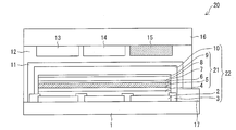
- FIG. 1 is a cross-sectional view schematically showing a schematic configuration of a main part of an organic EL display according to an embodiment of the present invention.
- FIG. 1 shows a portion of an organic EL element included in the organic EL display 20.
- the organic EL display 20 includes, as organic EL elements, a substrate 1, an organic EL unit 22, an inorganic sealing film 11, a resin sealing film 12, a red phosphor layer 13, and a green phosphor layer 14.
- An optical property adjusting layer 15, a sealing substrate 16, and a partition wall layer 17 are provided.
- the reflective electrode 2, the edge cover 3, the partition wall layer 17, the organic EL layer 21, and the translucent electrode 10 in the organic EL portion 22 are laminated in this order.
- an active element such as a TFT for driving the pixel, the organic EL display 20 or the like may be formed on the substrate 1.
- the partition wall layer 17 is an insulating layer formed outside the organic EL portion 22.
- the partition layer 17 can hold a coating liquid to be applied.
- the organic EL part 22 is composed of the reflective electrode 2, the semitransparent electrode 10, the organic EL layer 21, and the edge cover 3.
- the reflective electrode 2 and the translucent electrode 10 are a pair of electrodes that function as a pair, and sandwich the organic EL layer 21.
- the reflective electrode 2 is an anode and is an electrode that injects holes into the organic EL layer 21.
- the translucent electrode 10 is a cathode and an electrode that injects electrons into the organic EL layer 21.
- the organic EL layer 21 is a layer that emits blue light and is sandwiched between the reflective electrode 2 and the translucent electrode 10, and includes a light emitting layer 6 containing an organic light emitting material and a layer for injecting or transporting charges ( Hereinafter, a hole injection layer 4, a hole transport layer 5, a hole prevention layer 7, an electron transport layer 8, and an electron injection layer 9 functioning as a “charge injection transport layer”) are provided.
- the light emitted from the organic EL layer 21 passes through the translucent electrode 10 and is extracted outside.
- the edge cover 3 is an insulating cover formed between the reflective electrode 2 and the translucent electrode 10.
- the edge cover 3 can prevent leakage between the reflective electrode 2 and the translucent electrode 10 at the edge portion that becomes the end of the reflective electrode 2.
- the organic EL unit 22 uses the principle of a microcavity that utilizes multiple interference between the reflective electrode 2 and the translucent electrode 10, and has a structure that exhibits a so-called microcavity effect (optical microresonator structure). have. For example, it is more desirable to form the microcavity effect by setting the thickness between the reflective electrode 2 and the semitransparent electrode 10 so as to match the wavelength of light to be enhanced.
- the organic EL layer 21 is sandwiched between the pair of reflective electrodes 2 and the translucent electrode 10.
- the reflective electrode 2 is made of a mirror-surface totally reflective material
- the semi-transparent electrode 10 is made of a semi-transmissive material of a dielectric mirror
- the thickness of the organic EL layer 21 is formed so as to match the wavelength of light to be enhanced.
- the light component having a shifted wavelength is amplified to a desired wavelength by repeating multiple reflections between the reflective electrode 2 and the translucent electrode 10 and resonating. Output.
- the organic EL element having an optical microresonator structure can enhance light emission at a desired wavelength (see FIG. 10).
- the organic EL unit 22 in the present embodiment can enhance the intensity of light in the blue region.
- the distance between the reflective electrode 2 and the translucent electrode 10 can be adjusted by adjusting the film thickness of the organic EL layer 21.
- the inorganic sealing film 11 is a sealing film made of an inorganic compound
- the resin sealing film 12 is a sealing film made of a resin.
- the red phosphor layer 13 is a phosphor layer composed of a red phosphor that absorbs blue region light from the organic EL unit 22 and converts it into red region light, and functions as a red pixel.
- the green phosphor layer 14 is a phosphor layer composed of a green phosphor that absorbs blue region light from the organic EL unit 22 and converts it into green region light, and functions as a green pixel. Thereby, in the red pixel and the green pixel, the red phosphor layer 13 and the green phosphor layer 14 absorb light having directivity from the organic EL unit 22 having the optical microresonator structure, and isotropic. Light can be emitted.
- the light distribution characteristic adjustment layer 15 is a layer that adjusts the light distribution characteristic of the light from the organic EL unit 22, and functions as a blue pixel.
- the “light distribution characteristics” refer to characteristics relating to light brightness, color purity, and the like depending on viewing angles.
- the sealing substrate 16 is a substrate for sealing the above-described constituent members.
- Substrate 1 As the substrate 1, for example, an inorganic material substrate made of glass, quartz or the like, a plastic substrate made of polyethylene terephthalate, polycarbazole, polyimide or the like, an insulating substrate such as a ceramic substrate made of alumina or the like, aluminum (Al), iron (Fe ) And the like. Further, the surface of these substrates is coated with an insulator made of silicon oxide (SiO 2 ), an organic insulating material or the like, or the surface of a metal substrate made of Al or the like is insulated by a method such as anodic oxidation. It may be a coated substrate or the like.
- a plastic substrate or a metal substrate because a curved portion, a bent portion, and the like can be formed without stress.
- a substrate in which a plastic substrate is coated with an inorganic material or a substrate in which a metal substrate is coated with an inorganic insulating material is more preferable.
- leakage may occur due to the protrusion of the metal substrate, but such a problem can be prevented by the above-described configuration.
- the film thickness of the organic EL layer is often very thin, about 100 to 200 nm, and it is known that leakage (short-circuiting) occurs in the current in the pixel portion due to the protrusions of the substrate.
- a TFT may be formed on the substrate 1 as an active element.
- the substrate 1 it is preferable to use as the substrate 1 a substrate that does not melt at a temperature of 500 ° C. or less and does not cause distortion.
- a metal substrate it is preferable to use a metal substrate that is an iron-nickel alloy having a linear expansion coefficient of 1 ⁇ 10 ⁇ 5 / ° C. or less.
- substrate 1 is comparable as glass, TFT can be formed on the board
- a plastic substrate since the plastic substrate has a relatively low heat-resistant temperature, first, a TFT is formed on another glass substrate, and then this TFT is transferred onto the substrate 1, whereby the TFT Can be transferred and formed.
- FIG. 2 is a diagram showing a partial configuration of a circuit used by the organic EL display device according to the embodiment of the present invention.
- the circuit 30 includes a gate line 31, a signal line 32, a power supply line 33, a switching TFT 34, a driving TFT (active element) 35, a storage capacitor 36, an organic EL unit 22, and a ground line 38.
- the circuit 30 includes a plurality of gate lines 31 and a plurality of signal lines 32, and two TFTs, a switching TFT 34 and a driving TFT 35, are arranged for each pixel.
- the switching TFT 34 is disposed at the intersection between the gate line 31 and the signal line 32.
- the driving TFT 35 is electrically connected to the reflective electrode 2 in the organic EL unit 22. Note that the organic EL display 20 can be driven by a voltage-driven digital gradation method or the like.
- the circuit 30 may be electrically connected to an external drive circuit (scanning line electrode circuit (source driver), data signal electrode circuit (gate driver), power supply circuit) in order to drive each organic EL unit 22. Good.
- an external drive circuit scanning line electrode circuit (source driver), data signal electrode circuit (gate driver), power supply circuit
- the wavelength corresponding to the maximum value of the emission intensity of the light emitted from the organic EL unit 22 is preferably 400 nm or more and 480 nm or less.
- the maximum value of the light emission intensity of the light emitted from the organic EL portion 22 is reduced. If the wavelength corresponding to is 400 nm or more, the luminous efficiency and lifetime can be improved. In addition, the amount of absorption of the phosphor decreases with respect to light of 480 nm or more.
- the green phosphor generally has an abrupt decrease in absorption with respect to light having a long wavelength of 480 nm or longer. Therefore, if the wavelength is 480 nm or less, the phosphor, in particular, the green phosphor can be efficiently excited by the light from the organic EL unit 22 to emit light.
- the manufacturing cost and the material cost are significantly higher than those of the conventional separate coloring method in which the organic EL element is patterned into red, green, and blue pixels. It is possible to reduce it.
- this embodiment since the organic EL unit 22 having an optical microresonator structure is used, good light emission efficiency can be obtained and the lifetime can be extended, so that the cost and power consumption can be reduced. be able to. Furthermore, this embodiment can be suitably used as a large display and a display device.
- Organic EL layer 21 in this embodiment has a multilayer structure of the light emitting layer 6 and the charge injecting and transporting layer.
- the organic EL layer 21 is not limited to the configuration of the present embodiment, and may have the following configurations (1) to (9), for example.
- Each of the light emitting layer 6, the hole injection layer 4, the hole transport layer 5, the hole prevention layer 7, the electron prevention layer, the electron transport layer 8 and the electron injection layer 9 may have a single layer structure or a multilayer. It may be a structure.
- the film thickness of each layer in the organic EL layer 21 may be about 1 nm to 1000 nm, but is preferably 10 nm to 200 nm. If the film thickness is 10 nm or more, good physical properties (charge injection characteristics, transport characteristics, confinement characteristics, etc.) can be obtained for each layer of the organic EL layer 21. In addition, pixel defects due to foreign matters such as dust can be prevented. Moreover, if the film thickness is 200 nm or less, it is possible to prevent the drive voltage from increasing due to the resistance component of the organic EL layer 21 and to reduce power consumption.
- the light emitting layer 6 preferably contains a light emitting material (organic light emitting material) made of an organic compound.
- the light emitting layer 6 may be composed of, for example, only an organic light emitting material, or may be composed of a combination of a light emitting dopant and a host material.
- a hole transport material, an electron transport material, an additive (a donor, an acceptor, etc.) etc. may be contained arbitrarily.
- distributed in a polymeric material (binding resin) or an inorganic material may be sufficient. Especially, it is preferable to use what disperse
- the organic light emitting material a known light emitting material used for an organic EL layer or the like can be suitably used.
- a low molecular light emitting material, a polymer light emitting material, or the like can be used.
- a fluorescent material, a phosphorescent material, or the like can be used as the light-emitting material.
- Examples of the low-molecular light emitting material include fluorescent organic materials such as aromatic dimethylidene compounds, oxadiazole compounds, triazole derivatives, styrylbenzene compounds, and fluorenone derivatives.
- Examples of the aromatic dimethylidene compound include 4,4'-bis (2,2'-diphenylvinyl) -biphenyl (DPVBi).
- Examples of the oxadiazole compound include 5-methyl-2- [2- [4- (5-methyl-2-benzoxazolyl) phenyl] vinyl] benzoxazole.
- Examples of the triazole derivative include 3- (4-biphenylyl) -4-phenyl-5-t-butylphenyl-1,2,4-triazole (TAZ).
- Examples of the styrylbenzene compound include 1,4-bis (2-methylstyryl) benzene.
- polymer light emitting material examples include polyphenylene vinylene derivatives and polyspiro derivatives.
- polyphenylene vinylene derivative examples include poly (2-decyloxy-1,4-phenylene) (DO-PPP).
- polyspiro derivative examples include poly (9,9-dioctylfluorene) (PDAF).
- a known dopant material used for an organic EL layer or the like can be suitably used.
- dopant materials include fluorescent materials, phosphorescent organic metal complexes, and the like.
- fluorescent material include styryl derivatives.
- phosphorescent organometallic complexes include bis [(4,6-difluorophenyl) -pyridinato-N, C2 ′] picolinate iridium (III) (FIrpic), bis (4 ′, 6′-difluorophenylpolydinato) tetrakis ( 1-pyrazoyl) borate, iridium (III) (FIr6) and the like.
- a host material when using a dopant a known host material used for an organic EL layer or the like can be suitably used.
- host materials include the above-described low-molecular light-emitting materials, the above-described polymer light-emitting materials, carbazole derivatives, aniline derivatives, and fluorene derivatives.
- carbazole derivative include 4,4′-bis (carbazole) biphenyl, 9,9-di (4-dicarbazole-benzyl) fluorene (CPF), 3,6-bis (triphenylsilyl) carbazole (mCP), ( PCF).
- aniline derivatives include 4- (diphenylphosphoyl) -N, N-diphenylaniline (HM-A1).
- Fluorene derivatives include 1,3-bis (9-phenyl-9H-fluoren-9-yl) benzene (mDPFB), 1,4-bis (9-phenyl-9H-fluoren-9-yl) benzene (pDPFB) Etc.
- the charge injection transport layer is divided into a charge injection layer (hole injection layer 4 and electron injection layer 9) and a charge transport layer (hole transport layer 5 and electron transport layer 8).
- a charge injection layer hole injection layer 4 and electron injection layer 9
- a charge transport layer hole transport layer 5 and electron transport layer 8
- the charge injecting and transporting layer may be composed of only the materials exemplified below, but may optionally contain additives (donor, acceptor, etc.), etc., and these materials are polymeric materials (
- the resin may be dispersed in a binding resin) or an inorganic material.
- the material used for the charge injecting and transporting layer known materials used for the charge injecting and transporting layer such as an organic EL layer and an organic photoconductor can be used.
- the material includes a material for injecting or transporting holes (hereinafter also referred to as “hole injection / transport material”) and a material for injecting or transporting electrons (hereinafter also referred to as “electron injection / transport material”). Divided. Although these specific compounds are illustrated below, this invention is not limited to these materials.
- Examples of the hole injecting and transporting material include an oxide, an inorganic p-type semiconductor material, a porphyrin compound, an aromatic tertiary amine compound, a low molecular material, and a polymer material.
- Examples of the oxide include vanadium oxide (V 2 O 5 ) and molybdenum oxide (MoO 2 ).
- Aromatic tertiary amine compounds include N, N′-bis (3-methylphenyl) -N, N′-bis (phenyl) -benzidine (TPD), N, N′-di (naphthalen-1-yl) ) -N, N′-diphenyl-benzidine (NPD) and the like.
- low molecular weight material examples include hydrazone compounds, quinacridone compounds, styrylamine compounds, and the like.
- Polymer materials include polyaniline (PANI), polyaniline-camphor sulfonic acid (PANI-CSA), 3,4-polyethylenedioxythiophene / polystyrene sulfonate (PEDOT / PSS), poly (triphenylamine) derivative (Poly) -TPD), polyvinylcarbazole (PVCz), poly (p-phenylene vinylene) (PPV), poly (p-naphthalene vinylene) (PNV) and the like.
- the hole injection layer 4 it is preferable to use a material having a lower energy level of the highest occupied molecular orbital (HOMO) than the hole injection / transport material used for the hole transport layer 5.
- the hole transport layer 5 it is preferable to use a material having a higher hole mobility than the hole injection transport material used for the hole injection layer 4.
- the above-described hole injecting and transporting material doped with an acceptor.
- an acceptor the well-known acceptor material used for organic EL can be used. Although these specific compounds are illustrated below, this invention is not limited to these materials.
- the acceptor material examples include an inorganic material, a compound having a cyano group, a compound having a nitro group, and an organic material.
- Inorganic materials include gold (Au), platinum (Pt), tungsten (W), iridium (Ir), phosphoryl chloride (POCl 3 ), arsenic hexafluoride (AsF 6 ), chlorine (Cl), bromine (Br) , Iodine (I), vanadium oxide (V 2 O 5 ), molybdenum oxide (MoO 2 ), and the like.
- Examples of the compound having a cyano group include TCNQ (7,7,8,8, -tetracyanoquinodimethane), TCNQF 4 (tetrafluorotetracyanoquinodimethane), TCNE (tetracyanoethylene), HCNB (hexacyanobutadiene). And DDQ (dicyclodicyanobenzoquinone).
- Examples of the compound having a nitro group include TNF (trinitrofluorenone) and DNF (dinitrofluorenone).
- Examples of the organic material include fluoranyl, chloranil, bromanyl and the like. Among these, compounds having a cyano group such as TCNQ, TCNQF 4 , TCNE, HCNB, DDQ and the like are preferable because the carrier concentration can be increased more effectively.
- Examples of the electron injecting and transporting material include inorganic materials that are n-type semiconductors, oxadiazole derivatives, triazole derivatives, thiopyrazine dioxide derivatives, benzoquinone derivatives, naphthoquinone derivatives, anthraquinone derivatives, diphenoquinone derivatives, fluorenone derivatives, benzodifuran derivatives, etc. Low molecular materials; polymer materials such as poly (oxadiazole) (Poly-OXZ) and polystyrene derivatives (PSS) can be mentioned.
- examples of the electron injection material include fluorides such as lithium fluoride (LiF) and barium fluoride (BaF 2 ), and oxides such as lithium oxide (Li 2 O).
- the electron injection layer 9 it is preferable to use a material having a higher energy level of the lowest unoccupied molecular orbital (LUMO) than the electron injection transport material used for the electron transport layer 8.
- the electron transport layer 8 is preferably a material having a higher electron mobility than the electron injection transport material used for the electron injection layer 9.
- the electron injection / transport material In order to further improve the electron injection / transport property, it is preferable to dope the electron injection / transport material with a donor.
- a donor the well-known donor material used for organic EL can be used. Although these specific compounds are illustrated below, this invention is not limited to these materials.
- donor materials include inorganic materials, compounds having an aromatic tertiary amine as a skeleton, condensed polycyclic compounds, and organic materials.
- inorganic materials include alkali metals, alkaline earth metals, rare earth elements, Al, silver (Ag), copper (Cu), indium (In), and the like.
- Compounds having an aromatic tertiary amine skeleton include anilines, phenylenediamines, benzidines (N, N, N ′, N′-tetraphenylbenzidine, N, N′-bis- (3-methylphenyl) -N, N'-bis- (phenyl) -benzidine, N, N'-di (naphthalen-1-yl) -N, N'-diphenyl-benzidine, etc.), triphenylamines (triphenylamine, 4, 4′4 ′′ -tris (N, N-diphenyl-amino) -triphenylamine, 4,4′4 ′′ -tris (N-3-methylphenyl-N-phenyl-amino) -triphenylamine, 4 , 4′4 ′′ -tris (N- (1-naphthyl) -N-phenyl-amino) -triphenylamine, etc.), triphen
- Examples of the condensed polycyclic compound include phenanthrene, pyrene, perylene, anthracene, tetracene, and pentacene.
- the condensed polycyclic compound may have a substituent.
- Examples of the organic material include TTF (tetrathiafulvalene), dibenzofuran, phenothiazine, carbazole and the like.
- the donor material is preferably a compound having an aromatic tertiary amine as a skeleton, a condensed polycyclic compound, or an alkali metal among the materials described above. Thereby, the carrier concentration can be increased more effectively.
- the organic EL layer 21 is formed by using a coating solution (organic EL layer forming coating solution) in which the above materials are dissolved or dispersed in a solvent, using a spin coating method, a dipping method, a doctor blade method, a discharge coating method, or a spray coating method. It can be formed by a known wet process such as a coating method such as an ink jet method, a relief printing method, an intaglio printing method, a screen printing method, or a micro gravure coating method.
- a coating method such as an ink jet method, a relief printing method, an intaglio printing method, a screen printing method, or a micro gravure coating method.
- the organic EL layer 21 is formed from the above-described materials by a known dry process such as resistance heating vapor deposition, electron beam (EB) vapor deposition, molecular beam epitaxy (MBE), sputtering, or organic vapor deposition (OVPD). It can be formed by a laser transfer method or the like.
- the organic EL layer forming coating liquid may contain additives for adjusting the physical properties of the coating liquid, such as a leveling agent and a viscosity modifier. .
- a known electrode material can be used as the reflective electrode 2.
- the material used for the reflective electrode 2 include metals such as gold (Au), platinum (Pt), and nickel (Ni) having a work function of 4.5 eV or more. Thereby, the injection
- a material of the reflective electrode 2 it is preferable to use a material with high reflectivity that reflects light. Examples of such a material include reflective metals such as aluminum, silver, gold, aluminum-lithium alloy, aluminum-neodymium alloy, and aluminum-silicon alloy.
- the reflective electrode 2 include a combination of a transparent electrode and an electrode containing the above-described reflective metal (reflective electrode).
- an oxide (ITO) composed of indium (In) and tin (Sn), an oxide (SnO 2 ) of tin (Sn), an oxide composed of indium (In) and zinc (Zn). (IZO) etc. are mentioned.
- the translucent electrode 10 is preferably a translucent electrode. Thereby, the light from the organic EL layer 21 can be extracted efficiently.
- a semi-transparent electrode 10 may be composed of, for example, only a metal or a combination of a metal and a transparent electrode material.
- the metal that can be used for the translucent electrode include silver, magnesium, aluminum, a silver-magnesium alloy, and gold. Among these, silver is preferably used from the viewpoints of reflectance and transmittance.
- the film thickness of the reflective electrode 2 is preferably 50 nm or more.
- the wiring resistance increases, so that the drive voltage may increase. With the above-described configuration, such a risk can be prevented.
- the film thickness of the translucent electrode 10 is preferably 5 nm to 30 nm, and more preferably 10 nm to 30 nm. If the film thickness is 5 nm or more, light can be sufficiently reflected, so that the effect of interference can be sufficiently obtained. Further, if the film thickness is 10 nm or more, the effect of interference can be further enhanced. In addition, when the film thickness exceeds 30 nm, the light transmittance is drastically decreased, and thus the luminance and light emission efficiency may be decreased. However, if the film thickness is 30 nm or less, such a fear is excluded. can do.
- the reflective electrode 2 and the translucent electrode 10 can be formed using the above-described materials by a known method such as an EB vapor deposition method, a sputtering method, an ion plating method, or a resistance heating vapor deposition method.
- the reflective electrode 2 and the translucent electrode 10 can be patterned by a photolithographic fee method, a laser peeling method, or the like, if necessary. Further, a patterned electrode can be directly formed by combining with a shadow mask.
- the reflective electrode 2 and the translucent electrode 10 may be patterned so as to have a stripe shape. In this case, the direction of the stripes of the reflective electrode 2 and the stripes of the semitransparent electrode 10 is preferably orthogonal. With such a configuration, a good image with good viewing angle characteristics can be obtained.
- the organic EL unit 22 can emit light condensed in the front direction, that is, emit light having directivity. Therefore, it is possible to reduce the amount of light diffusing to the surroundings, and to increase the light emission efficiency in the front. As a result, the light emission energy generated in the light emitting layer 6 of the organic EL unit 22 can be efficiently propagated to the red pixel, the green pixel, and the blue pixel, and the front luminance can be increased.
- the emission spectrum of light from the organic EL unit 22 can be adjusted.
- the emission spectrum can be adjusted by adjusting the light to a desired emission peak wavelength and half width. Therefore, the red phosphor and the green phosphor can be adjusted to a spectrum that can be excited more effectively, and the color purity of light from the blue pixel can be improved. Therefore, effects such as an improvement in the color purity of light from the organic EL unit 22, an improvement in luminous efficiency, and an improvement in front luminance can be obtained.
- the organic EL unit 22 is not limited to the above-described configuration, and may have, for example, an optical microresonator structure using a dielectric multilayer film.
- An insulating material can be used for the edge cover 3.
- a known material can be used as the insulating material.
- an insulating material for example, an inorganic material, a resin material, or the like can be used.
- the inorganic material include silicon monoxide (SiO), silicon nitride oxide (SiON), silicon nitride (SiN), silicon oxycarbide (SiOC), silicon carbide (SiC), nitrogen-added hafnium silicate (HfSiON), zirconium monoxide ( ZrO), hafnium monoxide (HfO), lanthanum oxide (LaO), and the like.
- the resin material include acrylic and polyimide.
- the film thickness of the edge cover 3 is preferably 100 nm to 2000 nm. If the film thickness is 100 nm or more, it has sufficient insulation, so that leakage between the reflective electrode 2 and the translucent electrode 10 can be effectively prevented, power consumption can be suppressed, and non- Light emission can be prevented. If the film thickness is 2000 nm or less, the film forming process can be suppressed in a short time, so that productivity can be improved and disconnection of the translucent electrode 10 by the edge cover 3 can be prevented.
- the edge cover 3 can be formed using the above-described insulating material by a known method such as an EB vapor deposition method, a sputtering method, an ion plating method, or a resistance heating vapor deposition method. Further, for example, patterning can be performed by a known dry method or wet photolithography method.
- the red phosphor layer 13 and the green phosphor layer 14 may be composed of only a red phosphor or a green phosphor, and may further contain an additive or the like. Further, the red phosphor or the green phosphor may be dispersed in a polymer material (binding resin) or an inorganic material.
- the red phosphor and the green phosphor are in the form of particles, and the average particle diameter (d 50 ) is preferably 0.5 ⁇ m to 50 ⁇ m, and more preferably 1 ⁇ m to 50 ⁇ m. If the average particle diameter of the red phosphor and the green phosphor is 0.5 ⁇ m or more, a decrease in light emission efficiency can be suppressed, and if it is 1 ⁇ m or more, the light emission efficiency can be further increased. If the average particle diameter is 50 ⁇ m or less, it becomes easy to form a flat film as the phosphor layer, and a space is formed between the red phosphor layer 13 and the green phosphor layer 14 and the organic EL portion 22. Can be prevented.
- the red phosphor and the green phosphor when an inorganic material is used as the red phosphor and the green phosphor, between the organic EL portion 22 (refractive index: about 1.7) and the phosphor layer containing the inorganic material (refractive index: about 2.3). If a space (refractive index: 1.0) is created, the light from the organic EL unit 22 does not efficiently reach the red phosphor layer 13 and the green phosphor layer 14, so that the luminous efficiency of these phosphor layers is increased. The problem of deteriorating arises. However, the above-described configuration can prevent such a problem.
- the film thickness of the phosphor layer is preferably about 100 nm to 100 ⁇ m, more preferably 1 ⁇ m to 100 ⁇ m. If the film thickness is less than 100 nm, it is difficult to sufficiently absorb the blue light emitted from the organic EL unit 22, and the light emission efficiency is reduced, or the required color is mixed with blue transmitted light, and the color purity is deteriorated. Problems arise. Moreover, if the film thickness is 1 ⁇ m or more, the absorption of blue light emission from the organic EL portion 22 is increased, the blue transmitted light can be reduced, and good color purity can be obtained.
- the film thickness is 100 ⁇ m or less, the consumption of the material used for the phosphor layer can be suppressed within a range where the blue light emission from the organic EL portion 22 can be sufficiently absorbed. Therefore, with the above-described configuration, light emission efficiency can be increased and material cost can be suppressed.
- the phosphor materials described below can be used as the red phosphor and the green phosphor.
- the red phosphor and the green phosphor are preferably made of an inorganic material. Thereby, the red phosphor layer 13 and the green phosphor layer 14 can have high stability against degradation due to excitation light, degradation due to light emission, and the like.
- phosphor material As the phosphor material used as the red phosphor and the green phosphor, a known phosphor material can be used, and examples thereof include an organic phosphor material and an inorganic phosphor material.
- the organic phosphor material used as the green phosphor may be a fluorescent dye that converts blue excitation light into green light emission, and examples thereof include coumarin dyes and naphthalimide dyes.
- coumarin dyes include 2,3,5,6-1H, 4H-tetrahydro-8-trifluoromethylquinolidine (9,9a, 1-gh) coumarin (coumarin 153), 3- (2'-benzothiazolyl) -7-diethylaminocoumarin (coumarin 6), 3- (2'-benzimidazolyl) -7-N, N-diethylaminocoumarin (coumarin 7) and the like.
- naphthalimide dyes include basic yellow 51, solvent yellow 11, and solvent yellow 116.
- the organic phosphor material used as the red phosphor may be a fluorescent dye that converts blue excitation light into red light emission, and examples thereof include a cyanine dye, a pyridine dye, and a rhodamine dye.
- cyanine dyes include 4-dicyanomethylene-2-methyl-6- (p-dimethylaminostyryl) -4H-pyran.
- pyridine dye examples include 1-ethyl-2- [4- (p-dimethylaminophenyl) -1,3-butadienyl] -pyridinium-perchlorate.
- rhodamine dyes examples include rhodamine B, rhodamine 6G, rhodamine 3B, rhodamine 101, rhodamine 110, basic violet 11, and sulforhodamine 101.
- the inorganic phosphor material used as the green phosphor may be any phosphor that converts blue excitation light into green light emission.
- the inorganic phosphor material used as the red phosphor may be any phosphor that converts blue excitation light into red light emission.
- Y 2 O 2 S Eu 3+
- YAlO 3 Eu 3+
- Ca 2 Y 2 (SiO 4 ) 6 Eu 3+
- YVO 4 Eu 3+
- CaS Eu 3+
- Gd 2 O 3 Eu 3+
- Gd 2 O 2 S Eu 3+ Y (P, V) O 4 : Eu 3+ , Mg 4 GeO 5.5 F: Mn 4+ , Mg 4 GeO 6 : Mn 4+
- K 5 Eu 2.5 (WO 4 ) 6.25 Na 5 Eu 2 .5 (WO 4 ) 6.25
- K 5 Eu 2.5 (MoO 4 ) 6.25 Na 5 Eu 2.5 (MoO 4 ) 6.25
- Na 5 Eu 2.5 (MoO 4 ) 6.25 and the like.
- the inorganic phosphor may be subjected to surface modification treatment as necessary.
- the surface modification treatment include chemical treatment with a silane coupling agent or the like, physical treatment with addition of fine particles of submicron order, and a combination thereof.
- the red phosphor layer 13 and the green phosphor layer 14 may have a configuration in which the above-described phosphor material is dispersed in a polymer material.
- the polymer material examples include a polymer resin.
- a photosensitive resin is preferably used as the resin.
- the phosphor layer can be patterned by a photolithography method, and the red phosphor layer 13 and the green phosphor layer 14 can be easily manufactured.
- the polymer material may be one type of resin or a mixture of a plurality of types of resins.
- a photosensitive resin having a reactive vinyl group (photocurable resist material) or the like can be used as the photosensitive resin.
- examples thereof include acrylic resin, methacrylic resin, polyvinyl cinnamate resin, and hard rubber resin.
- the phosphor layer is formed, for example, by using a coating liquid (phosphor layer forming coating liquid) in which the above-described phosphor material and polymer material are dissolved and dispersed in a solvent, using a spin coating method, a dipping method, or a doctor blade method. It can be formed by a known wet process such as a coating method such as a discharge coating method or a spray coating method, an ink jet method, a relief printing method, an intaglio printing method, a screen printing method, or a printing method such as a micro gravure coating method.
- a coating method such as a discharge coating method or a spray coating method, an ink jet method, a relief printing method, an intaglio printing method, a screen printing method, or a printing method such as a micro gravure coating method.
- the phosphor layer is made of the above-described phosphor material, such as a resistance heating vapor deposition method, an electron beam (EB) vapor deposition method, a molecular beam epitaxy (MBE) method, a sputtering method, and an organic vapor deposition (OVPD) method. It can be formed by a known dry process or a laser transfer method.
- a resistance heating vapor deposition method such as an electron beam (EB) vapor deposition method, a molecular beam epitaxy (MBE) method, a sputtering method, and an organic vapor deposition (OVPD) method.
- EB electron beam
- MBE molecular beam epitaxy
- OVPD organic vapor deposition
- the red pixel and the green pixel can absorb light having directivity from the organic EL unit 22 and can extract red and green light emitted in the same direction to the outside. Therefore, it is possible to reduce or eliminate changes in luminance and color purity depending on the viewing angle.
- the light distribution characteristic adjusting layer 15 only needs to be configured to adjust the light distribution characteristic of the light from the organic EL layer 21.
- the light distribution characteristic adjustment layer 15 determines the luminance of the light from the organic EL layer 21 by the luminance of the light emitted from the red phosphor layer 13 and the luminance of the light emitted from the green phosphor layer 14. It is comprised so that it may adjust so that it may approach.
- the light distribution characteristic adjusting layer 15 changes the color purity of the light from the organic EL layer 21 to the color purity of the light emitted from the red phosphor layer 13 and the color purity of the light emitted from the green phosphor layer 14. It is comprised so that it may adjust so that it may approach.
- the light distribution characteristic adjusting layer 15 has the luminance of the light from the organic EL layer 21 and By adjusting the color purity, the light is adjusted to isotropic light.
- the blue pixel can emit isotropic light.
- the difference in luminance and color purity between the red, green, and blue pixels is small depending on the viewing angle.
- the luminance and color purity when the screen of the organic EL display 20 is viewed from the front and obliquely. Can be reduced.
- the light from the pixels of each color is isotropic, good viewing angle characteristics can be obtained. Therefore, a high quality organic EL display 20 can be provided.
- the light distribution characteristic adjusting layer 15 has the following formulas (1) and (2): 0.8L 60R / L 0R ⁇ L 60B / L 0B ⁇ 1.2L 60R / L 0R (1) 0.8L 60G / L 0G ⁇ L 60B / L 0B ⁇ 1.2L 60G / L 0G (2) It is preferable to adjust the light distribution characteristics (for example, light luminance) of the light from the organic EL layer 21 so as to satisfy the above.
- L 0R represents the luminance in the front direction of the light emitted from the red phosphor layer 13, and L 60R is a direction inclined by 60 degrees with respect to the front direction.
- L 0G indicates the luminance in the front direction of the light emitted from the green phosphor layer 14, and L 60G indicates the luminance in a direction inclined by 60 degrees with respect to the front direction.
- L 0B indicates the luminance in the front direction of the light emitted from the light distribution characteristic adjusting layer 15, and L 60B indicates the luminance in a direction inclined by 60 degrees with respect to the front direction.
- the light distribution characteristic adjustment layer 15 adjusts the luminance so as to satisfy the above formula (1), so that the front luminance of the light from the light distribution characteristic adjustment layer 15 and the light from the red phosphor layer 13 is inclined 60 degrees.
- the ratio with the brightness in degrees is adjusted so as to satisfy the relational expression shown in the above formula (1). Therefore, when the front luminance of the blue pixel and the red pixel is adjusted so that a desired emission color is obtained in the front direction, the blue pixel and the red pixel when viewed from the front direction and when viewed from the oblique direction The deviation of the luminance ratio can be reduced. Therefore, it is possible to reduce the deviation of the emission color between when viewed from the front direction and when viewed from the oblique direction to a level where it cannot be visually recognized.
- the front luminance of the light from the light distribution characteristic adjusting layer 15 and the light from the green phosphor layer 14 The ratio to the luminance at an angle of 60 degrees is adjusted so as to satisfy the relational expression shown in the above expression (2). Therefore, when the front luminance of the blue pixel and the green pixel is adjusted so that a desired emission color is obtained in the front direction, the blue pixel and the green pixel when viewed from the front direction and when viewed from the oblique direction The deviation of the luminance ratio can be reduced. Therefore, it is possible to reduce the deviation of the emission color between when viewed from the front direction and when viewed from the oblique direction to a level where it cannot be visually recognized.
- the light distribution characteristic adjustment layer 15 can bring the light distribution characteristic of light having directivity from the organic EL layer 21 closer to the light distribution characteristic of light emitted from the red phosphor layer 13 and the green phosphor layer 14. it can. Therefore, it is possible to suppress the deviation between the luminance of light from the red pixel and the green pixel and the luminance of light from the blue pixel when the screen of the organic EL display 20 is viewed obliquely to such an extent that it cannot be visually recognized.
- the light distribution characteristic adjusting layer 15 includes the following formulas (3) to (6):
- (x 0R , y 0R ) represents the color purity in the front direction of the light emitted from the red phosphor layer 13, and (x 60R , y 60R ) is The color purity in a direction inclined by 60 degrees with respect to the front direction. Further, (x 0G , y 0G ) indicates the color purity of the light emitted from the green phosphor layer 14 in the front direction, and (x 60G , y 60G ) is inclined by 60 degrees with respect to the front direction. Refers to the color purity in the direction.
- (x 0B , y 0B ) indicates the color purity in the front direction of the light emitted from the light distribution characteristic adjusting layer 15, and (x 60B , y 60B ) is inclined by 60 degrees with respect to the front direction. Refers to the color purity in the selected direction.
- the light from the light distribution characteristic adjusting layer 15 used without converting the light from the organic EL layer 21 changes not only the luminance but also the color purity depending on the viewing angle. That is, even when light from the light distribution characteristic adjustment layer 15 is adjusted so that the deviation between the front luminance and the luminance in the oblique direction is reduced, the color purity in the front direction and the color purity in the oblique direction may be different.
- a blue pixel and a green pixel are set so as to obtain a desired emission color in the front direction.
- the front luminance is adjusted, the deviation between the color purity when viewed from the front direction and the color purity when viewed from the oblique direction can be reduced. Therefore, the deviation between the emission color when viewed from the front direction and the emission color when viewed from the oblique direction, which may occur even when the deviation between the front luminance and the luminance in the oblique direction is reduced, cannot be visually recognized. It becomes possible to reduce to.
- the light distribution characteristic adjusting layer 15 for example, a layer having a characteristic of scattering light, a layer having a characteristic of diffusing light, or the like can be used.
- the “characteristic that scatters light” refers to a combination of a characteristic that diffracts light, a characteristic that refracts light, and a characteristic that reflects light.
- Examples of the light distribution characteristic adjusting layer 15 having the characteristic of scattering light include a form containing light scattering particles for scattering light.
- the light scattering particle is a particle having a property of scattering incident light by diffracting, refracting or reflecting it.
- the light scattering particles have an average particle diameter d 50 (B) of the following formulas (7) and (8): 0.8d 50 (B) ⁇ d 50 (R) ⁇ 1.2d 50 (B) ⁇ (7) 0.8d 50 (B) ⁇ d 50 (G) ⁇ 1.2d 50 (B) ⁇ (8) It is preferable to satisfy.
- d 50 (R) refers to the average particle diameter of the red phosphor
- d 50 (G) refers to the average particle diameter of the green phosphor.
- the light emitted from the light distribution characteristic adjusting layer 15 that is used without converting the light from the organic EL layer 21 is isotropically emitted from the phosphor layer (changes in luminance and color purity depending on the viewing angle). Unlike small, brightness and color purity change with viewing angle. Therefore, the luminance and color purity of the light of the red pixel and the green pixel and the light of the blue pixel differ depending on the viewing angle.
- the light distribution characteristic adjusting layer 15 scatters light from the organic EL layer 21 when the average particle diameters of the red phosphor, the green phosphor and the light scattering particles satisfy the above formulas (7) and (8).
- the light distribution characteristics can be adjusted to be close to the light distribution characteristics of light from the red and green pixels.
- the light distribution characteristic adjustment layer 15 can make the light distribution characteristic of light having directivity from the organic EL layer 21 closer to the light distribution characteristic of light emitted from the red phosphor layer 13 and the green phosphor layer 14. It becomes. Therefore, with the above-described configuration, the deviation between the luminance and color purity of the light emitted from the blue pixel and the luminance and color purity of the light emitted from the red pixel and the green pixel becomes very small. Therefore, the deviation between the luminance and color purity of red and green light and the luminance and color purity of blue light when the screen of the organic EL display 20 is viewed obliquely can be suppressed to an extent where it cannot be visually recognized.
- the light scattering particles are preferably particles (fine particles) having an average particle diameter (d 50 ) of 0.5 ⁇ m or more and 50 ⁇ m or less, and more preferably 1 ⁇ m or more and 50 ⁇ m or less.
- d 50 average particle diameter
- the average particle diameter of the light scattering particles is 1 ⁇ m or less, the particle diameter of the light scattering particles is small, and therefore the effect of adjusting the light distribution characteristics of the light in the blue region incident on the light distribution characteristics adjustment layer 15 to the desired characteristics. Is not enough. Therefore, the light intensity in the front direction of the emitted light becomes stronger than the light intensity in the oblique direction. If the average particle diameter is 0.5 ⁇ m or less, the tendency becomes more remarkable.
- the function of adjusting the light distribution characteristic by the light distribution characteristic adjustment layer 15 can be sufficiently extracted, and the light distribution characteristic is obtained. Can be adjusted satisfactorily. Therefore, deviation from the light distribution characteristics of the light from the red phosphor layer 13 and the green phosphor layer 14 can be suppressed.
- the average particle diameter of the light scattering particles is 50 ⁇ m or more, the unevenness of the surface of the light distribution characteristic adjusting layer 15 becomes large, and the effect of scattering due to the unevenness of the surface is larger than the scattering inside the light distribution characteristic adjusting layer 15. Therefore, the effect of adjusting the light distribution characteristic to a desired characteristic cannot be obtained.
- the average particle diameter of the light scattering particles is 50 ⁇ m or less, the unevenness of the surface of the light distribution characteristic adjusting layer 15 can be reduced, so that the light distribution characteristic of the light emitted from the light distribution characteristic adjusting layer 15 and the red phosphor The deviation from the light distribution characteristics of the light from the layer 13 and the green phosphor layer 14 can be reduced. Therefore, with the configuration described above, the luminance and color purity of the light emitted from the blue pixel can be made closer to the luminance and color purity of the light emitted from the red pixel and the green pixel. Angular characteristics can be obtained.
- the light distribution characteristic adjusting layer 15 may be composed of light scattering particles alone or may be composed of light scattering particles and a resin material. In the case of using a light scattering particle and a resin material, it is preferable that the light scattering particle is dispersed in the resin material or the like. Moreover, it is preferable that the refractive index of light-scattering particle
- the refractive index of the light scattering particles may be larger or smaller than the refractive index of the resin material or the like. The difference in refractive index is preferably as large as possible, and the refractive index ratio is preferably 1.1 to 1.5, and more preferably 1.2 to 1.3. Thereby, light having directivity can be efficiently converted into isotropic light.
- the property of light scattering by the light distribution characteristic adjusting layer 15 greatly depends on the particle diameter (d) of the light scattering particles and the wavelength ( ⁇ ) of the incident light.
- Mie scattering is preferable because the amount of light scattered forward can be increased more than the amount of light scattered backward. That is, it is preferable that the particle diameter of the light scattering particle and the wavelength of incident light are substantially equal.
- the light distribution characteristic adjustment layer 15 can be produced with a simple configuration because the light distribution characteristic of only blue light has to be adjusted. For example, when adjusting the light distribution characteristics for light of two or more colors, the light distribution characteristics need to be adjusted for each wavelength of light of each color, and the light distribution characteristic adjustment layer is patterned for each color. It is necessary to make it. In this case, there arises a problem that the configuration and the process are complicated. However, the present invention can prevent such problems from occurring.
- Light scattering particles Next, the light scattering particles will be described in detail.
- the light scattering particles may be made of an organic material or may be made of an inorganic material, but is preferably made of an inorganic material. Thereby, it becomes possible to diffuse or scatter light having directivity from the organic EL unit 22 more isotropically and effectively. Moreover, it becomes possible to provide the light distribution characteristic adjustment layer 15 stable to light and heat by using an inorganic material.
- the light scattering particles have high transparency.
- the refractive index ratio with a resin material is contained in the numerical range mentioned above.
- the main component is an oxide of at least one metal selected from the group consisting of silicon, titanium, zirconium, aluminum, indium, zinc, tin, and antimony. Examples thereof include particles (fine particles).
- particles (inorganic fine particles) made of an inorganic material for example, silica beads (refractive index: 1.44), alumina beads (refractive index: 1.63), titanium oxide.
- examples thereof include beads (refractive index: anatase type: 2.50, rutile type: 2.70), zirconia oxide beads (refractive index: 2.05), and zinc oxide beads (refractive index: 2.00).
- particles (organic fine particles) made of an organic material are used as the light scattering particles, for example, polymethyl methacrylate beads (refractive index: 1.49), acrylic beads (refractive index: 1.50), acrylic- Styrene copolymer beads (refractive index: 1.54), melamine beads (refractive index: 1.57), high refractive index melamine beads (refractive index: 1.65), polycarbonate beads (refractive index: 1.57), Styrene beads (refractive index: 1.60), crosslinked polystyrene beads (refractive index: 1.61), polyvinyl chloride beads (refractive index: 1.60), benzoguanamine-melamine formaldehyde beads (refractive index: 1.68), Examples thereof include silicone beads (refractive index: 1.50).
- the resin material that can be used for the light distribution characteristic adjusting layer 15 is preferably a translucent resin.
- the resin material include melamine resin (refractive index: 1.57), nylon (refractive index: 1.53), polystyrene (refractive index: 1.60), melamine beads (refractive index: 1.57).
- Polycarbonate (refractive index: 1.57), polyvinyl chloride (refractive index: 1.60), polyvinylidene chloride (refractive index: 1.61), polyvinyl acetate (refractive index: 1.46), polyethylene (refractive Ratio: 1.53), polymethyl methacrylate (refractive index: 1.49), poly MBS (refractive index: 1.54), medium density polyethylene (refractive index: 1.53), high density polyethylene (refractive index: 1.54), tetrafluoroethylene (refractive index: 1.35), polytrifluoroethylene chloride (refractive index: 1.42), polytetrafluoroethylene (refractive index: 1.35), and the like.
- the light distribution characteristic adjustment layer 15 is not limited to the above-described configuration, and may be any layer that adjusts the luminance and color purity of light from the organic EL layer 21 as described above.
- optical members such as a micro lens and a prism, can be used, for example.
- the light distribution characteristic adjustment layer 15 may be provided, for example, on the surface of the sealing substrate 16 from which light is emitted.
- the organic EL display 20 is such that a human being cannot visually recognize a shift in light distribution characteristics (change in luminance and chromaticity depending on viewing angle) of light from red pixels, green pixels, and blue pixels. Can be reduced. Thereby, it is possible to eliminate various problems caused by the difference in the light distribution characteristics of red, green and blue light.
- Various problems include, for example, when red and green light is isotropic and blue light is directional light in the front direction, it is adjusted to look white when viewed from the front direction. Even when the image is viewed from an oblique direction, the luminance of blue is relatively lower than that of red and green, so that the image appears to be shifted in the yellow direction.
- the present embodiment is configured by pixels that emit red, green, and blue, so that it is possible to obtain a full-color image by adjusting the luminance of light of each color.
- pixels that emit cyan, yellow, and the like it is preferable to add pixels that emit cyan, yellow, and the like as necessary.
- the color purity of light from pixels emitting cyan and yellow is preferably located outside the triangle connected by points indicating the color purity of pixels emitting red, green and blue on the chromaticity diagram. .
- Inorganic sealing film 11 and resin sealing film 12 As the inorganic sealing film 11 and the resin sealing film 12, known materials and sealing methods can be used.
- the material used for the inorganic sealing film 11 is preferably a light transmissive material.
- the inorganic sealing film 11 include those in which an inert gas such as nitrogen gas or argon gas is sealed with glass, metal, or the like. Moreover, it is preferable to mix hygroscopic agents, such as barium oxide, in the enclosed inert gas. Thereby, deterioration of organic EL by a water
- the resin used for the resin sealing film 12 a known material can be used as long as it is a light-transmitting resin.
- a method of forming the resin sealing film 12 a method of applying a resin on the inorganic sealing film 11 formed on the semitransparent electrode 10 using a spin coat method, ODF, or a laminate method, or semitransparent A method of bonding the electrode 10 and a resin film can be used.
- the organic EL display 20 may be configured not to include the inorganic sealing film 11.
- the resin sealing film 12 can be directly formed on the translucent electrode 10 by the method described above.
- the inorganic sealing film 11 and the resin sealing film 12 can prevent the entry of oxygen or moisture into the organic EL part 22 from the outside, and the life of the organic EL part 22 is improved. In addition, damage to the organic EL portion 22 and the like when the sealing substrate 16 is bonded to the substrate 1 can be reduced.
- the sealing substrate 16 As the sealing substrate 16, a known material and a sealing method can be used.
- the sealing substrate 16 is preferably transparent or translucent.
- a substrate made of glass, plastic, or the like can be used. Thereby, the light from the red pixel, the green pixel, and the blue pixel can pass through the sealing substrate 16.
- the sealing substrate 16 is the substrate 1 on which the organic EL portion 22 and the like are formed after the red phosphor layer 13, the green phosphor layer 14, and the light distribution characteristic adjusting layer 15 are formed on the surface facing the substrate 1. And may be pasted together. In that case, it is preferable to flatten by forming a flattening film or the like to be described later on the red phosphor layer 13, the green phosphor layer 14, and the light distribution characteristic adjusting layer 15 on the sealing substrate 16. . Thereby, it is possible to prevent a space from being formed between the organic EL unit 22 and the red phosphor layer 13, the green phosphor layer 14, and the light distribution characteristic adjusting layer 15, and the adhesion between the substrate 1 and the sealing substrate 16. Can be improved.
- the organic EL display 20 may further include a low reflection film and a color filter. Each configuration will be described below.
- the low reflection film can be provided between the color filters, between the phosphor layers, between the phosphor layer, and the light distribution characteristic adjusting layer 15. Since each light emission of RGB is emphasized by the low reflection film, visibility can be improved.
- a known material can be used, and examples thereof include an inorganic material and an organic material.
- the inorganic material include silicon oxide (SiO 2 ), silicon nitride (SiN or Si 2 N 4 ), tantalum oxide (TaO or Ta 2 O 5 ), and the like.
- the organic material include an acrylic resin and a resist material.
- Examples of the method for forming the low-reflection film include a chemical vapor deposition (CVD) method, a dry process such as a vacuum deposition method, and a wet process such as a spin coating method. Moreover, it can also pattern by the photolithographic method etc. as needed.
- CVD chemical vapor deposition
- dry process such as a vacuum deposition method
- wet process such as a spin coating method.
- it can also pattern by the photolithographic method etc. as needed.
- the color filter is preferably provided on the light emission surface of the red phosphor layer 13, the green phosphor layer 14, and the light distribution characteristic adjustment layer 15.
- the color filter can be provided, for example, between the sealing substrate 16 and the red phosphor layer 13, the green phosphor layer 14, and the light distribution characteristic adjustment layer 15.
- a known color filter can be used as the color filter.
- the color filter by providing the color filter, the color purity of the red pixel, the green pixel, and the blue pixel can be increased, and the color reproduction range of the organic EL display 20 and the organic EL display device including the same can be expanded. it can.
- a green color filter is preferably formed on the green phosphor layer 14.
- the red color filter and the green color filter absorb the blue component and ultraviolet component of the external light, so that it is possible to reduce or prevent light emission by the external light of each phosphor layer, and to reduce or prevent the decrease in contrast. Can do.
- FIG. 3 is a cross-sectional view schematically showing a configuration of a main part of an organic EL display according to another embodiment of the present invention.
- FIG. 3 shows a portion of the organic EL element included in the organic EL display 40.
- constituent elements having the same functions as those of the constituent elements according to the first embodiment are given the same numbers, and explanation thereof is omitted. In the present embodiment, differences from the first embodiment will be mainly described.
- the organic EL display 40 is an active matrix drive type, and includes a substrate 1, a gate electrode 41, a drain electrode 42, a source electrode 43, a gate insulating film 44, a wiring 45, a through hole 46, and a planarizing film. 47, the organic EL part 22, the inorganic sealing film 11, the resin sealing film 12, the red phosphor layer 13, the green phosphor layer 14, the light distribution characteristic adjusting layer 15, the black matrix 48, A sealing substrate 16 is used.
- the organic EL display 40 includes a TFT as an active element, and drives the organic EL unit 22 in an active matrix. Therefore, excellent display quality can be obtained. In addition, since the light emission time can be made longer than in the case of passive driving, it is possible to reduce the driving voltage for obtaining a desired luminance and to reduce power consumption.
- a gate electrode 41 constituting a plurality of gate lines and a source electrode constituting a plurality of signal lines are formed, and a TFT is arranged at an intersection of the gate electrode 41 and the source electrode 43. Is done.
- a planarizing film 47 is formed on the TFT. That is, the TFT is provided on the side opposite to the organic EL layer 21 with respect to the reflective electrode 2.
- the organic EL display 40 is driven by a voltage-driven digital gradation method, and two TFTs for switching and driving are arranged for each pixel.
- the driving TFT and the reflective electrode 2 of the organic EL portion 22 are electrically connected through a contact hole formed in the planarizing film 47.
- a capacitor for setting the gate potential of the driving TFT to a constant potential is arranged so as to be connected to the gate electrode 41 of the driving TFT.
- the present invention is not limited to the voltage-driven digital gradation method, and may be driven by a current-driven analog gradation method.
- the configuration of the TFT may include two or more TFTs with a compensation circuit built in the pixel. If the organic EL unit 22 is driven by the TFT having such a configuration, variations in TFT characteristics (mobility, threshold voltage) can be prevented.
- a black matrix 48 is formed between the red phosphor layer 13, the green phosphor layer 14, and the light distribution characteristic adjusting layer 15.
- the TFT is preferably formed on the substrate 1 in advance before forming the organic EL portion 22.
- Examples of the TFT include those that function for switching and driving.
- a known TFT can be used.
- a metal-insulator-metal (MIM) diode can be used instead of the TFT.
- TFT that can be used for the organic EL display 40
- known materials, structures, and formation methods can be used.
- the material of the active layer of TFT for example, amorphous silicon (amorphous silicon), polycrystalline silicon (polysilicon), microcrystalline silicon, inorganic semiconductor materials such as cadmium selenide, zinc oxide, indium oxide-gallium oxide- Examples thereof include oxide semiconductor materials such as zinc oxide, organic semiconductor materials such as polythiophene derivatives, thiophene oligomers, poly (p-ferylene vinylene) derivatives, naphthacene, and pentacene.
- the TFT structure include a staggered type, an inverted staggered type, a top gate type, and a coplanar type.
- a method for forming an active layer constituting a TFT (1) a method of ion doping impurities into amorphous silicon formed by a plasma induced chemical vapor deposition (PECVD) method or the like, and (2) a silane (SiH 4 ) gas is used.
- PECVD plasma induced chemical vapor deposition
- SiH 4 silane
- LPCVD low pressure chemical vapor deposition
- the gate insulating film 44 of the TFT used in this embodiment can be formed using a known material.
- PECVD method SiO 2 was formed by the LPCVD method or the like, SiO 2 or the like obtained by the polysilicon film by thermal oxidation and the like.
- the source electrode 43, the gate electrode 41, and the drain electrode 42 of the TFT used in the present embodiment can be formed using known materials, for example, tantalum (Ta), aluminum (Al), copper (Cu ) And the like.
- the TFT of the organic EL display 40 can be formed with the above-described configuration, but is not limited to these materials, structures, and formation methods.
- the planarizing film 47 is formed on the TFT formed on the substrate 1.
- the present invention is not limited to such a configuration.
- an interlayer insulating film may be formed on the TFT, and the planarizing film 47 may be provided on the interlayer insulating film.
- the organic EL display 40 since the TFT is formed on the substrate 1, irregularities are formed on the surface thereof.
- the organic EL portion 22 is directly formed on the surface, due to the unevenness, for example, the defect of the reflective electrode 2, the defect of the organic EL layer 21, the disconnection of the semitransparent electrode 10, the reflection electrode 2 and the semitransparent electrode 10 There is a risk that defects in the organic EL part 22 such as short circuiting and lowering of breakdown voltage may occur.
- the planarization film 47 can be formed using a known material, and examples thereof include inorganic materials such as silicon oxide, silicon nitride, and tantalum oxide, and organic materials such as polyimide, acrylic resin, and resist material.
- examples of the method for forming the planarizing film 47 include a dry process such as a CVD method and a vacuum deposition method, and a wet process such as a spin coating method. Further, the planarization film 47 may have a single layer structure or a multilayer structure.
- FIG. 4 is a cross-sectional view schematically showing a configuration of a main part of an organic EL display according to another embodiment of the present invention.
- FIG. 4 shows a portion of the organic EL element included in the organic EL display 60.
- constituent elements having the same functions as those of the constituent elements according to the first embodiment are given the same numbers, and explanation thereof is omitted. In the present embodiment, differences from the first embodiment will be mainly described.
- the organic EL display 60 includes a substrate 1, an organic EL unit 22, an inorganic sealing film 11, a resin sealing film 12, a polarizing film (polarizing plate) 61, a substrate 62, a transparent electrode 63, and an alignment film. 64, a liquid crystal layer 65, a planarizing film 66, a red phosphor layer 13, a green phosphor layer 14, a light distribution characteristic adjusting layer 15, and a sealing substrate 16.
- the resin sealing film 12 between the resin sealing film 12, the red phosphor layer 13, the green phosphor layer 14, and the light distribution characteristic adjusting layer 15, the polarizing film 61, the substrate 62, the transparent electrode 63.
- an alignment film 64, a liquid crystal layer 65, and a planarizing film 66 are provided.
- the substrate 62, the polarizing film 61, the transparent electrode 63, the alignment film 64, and the liquid crystal layer 65 function as so-called switching elements.
- the substrate 62 is a substrate for forming the transparent electrode 63.
- the polarizing film 61 is a layer for controlling the transmittance of the liquid crystal layer 65.
- the transparent electrode 63 is an electrode for driving the liquid crystal layer 65.
- the alignment film 64 is a film for aligning the liquid crystal of the liquid crystal layer 65.
- the liquid crystal layer 65 is driven when a voltage is applied to switch the red pixel, the green pixel, and the blue pixel. Thereby, an excellent display quality can be obtained.
- a known material can be used for the substrate 62, the transparent electrode 63, the alignment film 64, and the liquid crystal layer 65.
- the planarizing film 66 is formed between the polarizing film 61 and the red phosphor layer 13, the green phosphor layer 14, and the light distribution characteristic adjusting layer 15.
- the same film as the planarizing film 47 in the second embodiment can be used.
- the planarization film 66 can prevent a space from being formed between the polarizing film 61 and the red phosphor layer 13, the green phosphor layer 14, and the light distribution characteristic adjustment layer 15.
- the light distribution characteristic adjusting layer emits the luminance of light from the organic EL layer from the luminance of light emitted from the red phosphor layer and the green phosphor layer. And adjusting the color purity of the light from the organic EL layer to the color purity of the light emitted from the red phosphor layer and the light emitted from the green phosphor layer. It is preferable to adjust the color purity so as to approach the color purity.
- a blue pixel will bring the brightness
- the difference in luminance and color purity between the pixels of each color depending on the viewing angle is small, so that it is possible to reduce the change in the balance of the luminance and color purity of each color when viewed from the front and obliquely.
- the light from the pixels of each color is isotropic, good viewing angle characteristics can be obtained.
- the luminance in the front direction is L0R
- the luminance in the direction inclined by 60 degrees with respect to the front direction is L. 60R
- the luminance in the front direction of the light emitted from the green phosphor layer is L 0G
- the luminance in the direction inclined by 60 degrees with respect to the front direction is L 60G
- the light distribution characteristic adjustment layer is as follows: Formulas (1) and (2) 0.8L 60R / L 0R ⁇ L 60B / L 0B ⁇ 1.2L 60R / L 0R (1) 0.8L 60G / L 0G ⁇ L 60B / L 0B ⁇ 1.2L 60G / L 0G (2) It is preferable to adjust the
- the deviation between the luminance of the light emitted from the blue pixel and the luminance of the light emitted from the red phosphor layer and the green phosphor layer is very small.
- the deviation between the luminance of red and green light and the luminance of blue light can be suppressed to the extent that it cannot be visually recognized.
- the color purity in the front direction out of the light emitted from the red phosphor layer is set to (x 0R , y 0R ) and tilted by 60 degrees with respect to the front direction.
- the color purity in the measured direction is (x 60R , y 60R )
- the color purity in the front direction of the light emitted from the green phosphor layer is (x 0G , y 0G ), and 60 % with respect to the front direction.
- the color purity in the inclined direction is (x 60G , y 60G )
- the color purity in the front direction of the light emitted from the light distribution characteristic adjusting layer is (x 0B , y 0B )
- the front direction When the color purity in a direction inclined by 60 degrees is (x 60B , y 60B ), the light distribution characteristic adjusting layer has the following formulas (3) to (6):
- the deviation between the color purity of the light emitted from the blue pixel and the color purity of the light emitted from the red phosphor layer and the green phosphor layer is very small.
- the difference between the color purity of the red and green light and the color purity of the blue light can be suppressed to the extent that it cannot be visually recognized.
- the wavelength corresponding to the maximum value of the light emission intensity of the light emitted from the organic EL layer is 400 nm or more and 480 nm or less.
- the wavelength corresponding to the maximum value of the light emission intensity of the light emitted from the organic EL layer is 400 nm or more, the light emission efficiency and the life can be improved. Moreover, since the said wavelength is 480 nm or less, a fluorescent substance layer, especially a green fluorescent substance layer can be efficiently excited by the light from an organic electroluminescent layer, and can be light-emitted.
- the light distribution characteristic adjusting layer includes light scattering particles for scattering light, and an average particle diameter of the red phosphor included in the red phosphor layer is d 50.
- R when the average particle diameter of the green phosphor included in the green phosphor layer is d 50 (G) and the average particle diameter of the light scattering particles is d 50 (B) , the following formula (7) and (8) 0.8d 50 (B) ⁇ d 50 (R) ⁇ 1.2d 50 (B) ⁇ (7) 0.8d 50 (B) ⁇ d 50 (G) ⁇ 1.2d 50 (B) ⁇ (8) It is preferable to satisfy.
- emitted from a red fluorescent substance layer and a green fluorescent substance layer becomes very small. .
- the deviation between the luminance and color purity of red and green light and the luminance and color purity of blue light when viewed from an oblique direction can be suppressed to an extent where it cannot be visually recognized.
- the light scattering particles are preferably made of an inorganic material.
- the light scattering particles preferably have an average particle diameter of 1 ⁇ m or more and 50 ⁇ m or less.
- the average particle diameter of the light scattering particles is 1 ⁇ m or less, the particle diameter of the light scattering particles is small, so that the effect of adjusting the light distribution characteristics cannot be sufficiently obtained. Optical characteristics can be adjusted satisfactorily. Further, if the average particle diameter of the light scattering particles is 50 ⁇ m or more, the unevenness of the surface of the light distribution characteristic adjustment layer becomes large, and the scattering on the surface becomes more dominant than the scattering inside the light distribution characteristic adjustment layer, The effect of adjusting the light distribution characteristic to a desired characteristic cannot be obtained. However, with the above configuration, the unevenness on the surface of the light distribution characteristic adjusting layer can be reduced, and thus the light distribution characteristic can be adjusted favorably.
- the luminance and color purity of the light emitted from the blue pixel can be made closer to the luminance and color purity of the light emitted from the red phosphor layer and the green phosphor layer. It is possible to obtain good viewing angle characteristics.
- the organic EL device it is preferable that at least one of the red phosphor included in the red phosphor layer and the green phosphor included in the green phosphor layer is made of an inorganic material.
- red fluorescent substance layer or green fluorescent substance layer containing what was comprised with the inorganic material among red fluorescent substance and green fluorescent substance be a layer (film
- the average particle diameter of at least one of the red phosphor included in the red phosphor layer and the green phosphor included in the green phosphor layer is 0.5 ⁇ m or more and 50 ⁇ m or less. It is preferable.
- the average particle diameter of the phosphor is 0.5 ⁇ m or more, high luminous efficiency can be obtained.
- the average particle diameter is 50 ⁇ m or less, it becomes easy to form a flat film as the red phosphor layer or the green phosphor layer, and a space is formed between the surrounding layers, resulting in a decrease in luminous efficiency. Can be prevented.
- the translucent electrode contains silver. If it is said structure, the reflectance and transmittance
- the film thickness of the translucent electrode is 10 nm or more and 30 nm or less.
- the film thickness is 10 nm or more, the light can be sufficiently reflected by the translucent electrode, so that a high interference effect can be obtained. Further, since the film thickness is 30 nm or less, light can be transmitted efficiently, and sufficient luminance and light emission efficiency can be obtained.
- the organic EL layer contains a phosphorescent material that emits phosphorescence in a blue region.
- a color filter is provided on the light emission surface of the red phosphor layer, the green phosphor layer, and the light distribution characteristic adjusting layer.
- the color purity of the light emitted from the red phosphor layer, the green phosphor layer, and the light distribution characteristic adjusting layer can be increased. Therefore, when used in an organic EL display, the color reproduction range can be expanded.
- a polarizing plate is provided on the side opposite to the organic EL layer with respect to the semitransparent electrode.
- the red phosphor layer and the green fluorescent layer are disposed between the organic EL layer and the red phosphor layer, the green phosphor layer, and the light distribution characteristic adjusting layer. It is preferable to provide a liquid crystal layer for switching the body layer and the light distribution characteristic adjusting layer.
- the liquid crystal layer functions as a so-called switching element, it is possible to provide an organic EL display with excellent display quality when used in an organic EL display.
- the organic EL display according to the present invention preferably includes an active element that drives the organic EL element in an active matrix.
- the above configuration can provide an organic EL display with excellent display quality.
- the light emission time can be made longer than in the case of passive driving, it is possible to reduce the driving voltage for obtaining a desired luminance and to reduce power consumption.
- the active element is provided on the side opposite to the organic EL layer with respect to the reflective electrode.
- the aperture ratio can be increased without considering the wiring in the active element. Therefore, it is possible to provide an organic EL display with low power consumption.
- Example 1 An organic EL display device including an organic EL display having the same configuration as the organic EL display 20 in the first embodiment described above was produced. Hereinafter, the same member number is attached to a member having the same function as a constituent member of the organic EL display 20.
- the substrate 1 organic EL element substrate on which the organic EL part 22 was formed was produced.
- a glass substrate having a thickness of 0.7 mm was used as the substrate 1.
- a silver film is formed on the substrate 1 to a thickness of 100 nm by sputtering, and an indium-tin oxide (ITO) film is formed on the substrate 1 to a thickness of 20 nm by sputtering.
- ITO indium-tin oxide
- the reflective electrode 2 was patterned into 90 stripes with a width of 2 mm by a known photolithography method.
- the partition layer 17 has a structure in which the short side of the reflective electrode 2 is covered with SiO 2 by 10 ⁇ m from the end. After washing with water, pure water ultrasonic cleaning was performed for 10 minutes, acetone ultrasonic cleaning for 10 minutes, and isopropyl alcohol vapor cleaning for 5 minutes, followed by drying at 100 ° C. for 1 hour.
- the substrate 1 was fixed to a substrate holder in an inline type resistance heating vapor deposition apparatus, and after reducing the pressure to 1 ⁇ 10 ⁇ 4 Pa or less, each organic layer in the organic EL layer 21 was formed.
- a hole injection layer 4 having a film thickness of 120 nm was formed by resistance heating vapor deposition using 1,1-bis-di-4-tolylamino-phenyl-cyclohexane (TAPC) as a hole injection material.
- TAPC 1,1-bis-di-4-tolylamino-phenyl-cyclohexane
- N, N′-di-1-naphthyl-N, N′-diphenyl-1,1′-biphenyl-1,1′-biphenyl-4,4′-diamine is used as a hole transport material.
- a hole transport layer 5 having a thickness of 40 nm was formed by resistance heating vapor deposition.
- This blue organic light-emitting layer comprises 1,4-bis-triphenylsilyl-benzene (UGH-2) (host material) and bis [(4,6-difluorophenyl) -pyridinato-N, C2 ′] picolinate iridium (III ) (FIrpic) (blue phosphorescent light-emitting dopant) and the vapor deposition rates were 1.5 ⁇ / sec and 0.2 ⁇ / sec, respectively.
- UH-2 1,4-bis-triphenylsilyl-benzene
- FIrpic picolinate iridium
- a hole blocking layer 7 (thickness: 10 nm) was formed on the light emitting layer 6 using 2,9-dimethyl-4,7-diphenyl-1,10-phenanthroline (BCP).
- BCP 2,9-dimethyl-4,7-diphenyl-1,10-phenanthroline
- an electron transport layer 8 (thickness: 30 nm) was formed on the hole blocking layer 7 using tris (8-hydroxyquinoline) aluminum (Alq 3 ).
- an electron injection layer 9 (thickness: 0.5 nm) was formed on the electron transport layer 8 using lithium fluoride (LiF).
- a translucent electrode 10 was formed.
- the substrate 1 was fixed to a metal deposition chamber.
- a shadow mask for forming a translucent electrode (a mask in which an opening is formed so that the translucent electrode 10 can be formed in a stripe shape having a width of 2 mm in a direction perpendicular to the long side direction of the reflective electrode 2)
- the substrate 1 are aligned, and magnesium and silver are co-deposited on the surface of the electron injection layer 9 by a vacuum deposition method at a deposition rate of 0.1 ⁇ / sec and 0.9 ⁇ / sec, respectively. In a desired pattern.
- the peak wavelength of the light emitted from the organic EL part 22 due to the microcavity effect among the light emitted from the organic EL layer 21 is 460 nm, the half width.
- the half width. was set to an optical distance (total organic film thickness: 230 nm) such that the thickness was 50 nm.
- the produced organic EL part 22 has a microcavity effect (interference effect) between the reflective electrode 2 and the translucent electrode 10 and can emit light with high front luminance. Therefore, the light emission energy from the organic EL part 22 can be efficiently propagated by the red phosphor layer 13, the green phosphor layer 14, and the light distribution characteristic adjustment layer 15.
- an inorganic sealing film 11 made of 3 ⁇ m of SiO 2 was formed by plasma CVD.
- the inorganic sealing film 11 was patterned using a shadow mask from the top, bottom, left, and right ends of the display portion to a region (sealing area) having a width of 2 mm.
- the display unit refers to a part where an image is displayed.
- a sealing substrate 16 (phosphor substrate) on which the red phosphor layer 13, the green phosphor layer 14, and the light distribution characteristic adjusting layer 15 were formed was produced.
- red phosphor layer 13 15 g of ethanol and 0.22 g of ⁇ -glycidoxypropyltriethoxysilane were added to 0.16 g of aerosil having an average particle diameter of 5 nm, and the mixture was stirred at room temperature for 1 hour in an open system. Next, this mixture and 20 g of red phosphor K 5 Eu 2.5 (WO 4 ) 6.25 having an average particle size (d 50 (R) ) of 1.0 ⁇ m were transferred to a mortar, and thoroughly mixed. Heating was performed in an oven at 70 ° C. for 2 hours and further in an oven at 120 ° C. for 2 hours to obtain surface-modified K 5 Eu 2.5 (WO 4 ) 6.25 .
- the green phosphor layer 14 15 g of ethanol and 0.22 g of ⁇ -glycidoxypropyltriethoxysilane were added to 0.16 g of aerosil having an average particle size of 5 nm, and the mixture was stirred at room temperature for 1 hour in an open system.
- the mixture and 20 g of green phosphor Ba 2 SiO 4 : Eu 2+ with an average particle size (d 50 (G) ) of 1.0 ⁇ m were transferred to a mortar, thoroughly mixed, and then further heated in an oven at 70 ° C. for 2 hours. Heating was performed in an oven at 120 ° C. for 2 hours to obtain surface-modified Ba 2 SiO 4 : Eu 2+ .
- the formation of the light distribution characteristic adjusting layer 15 will be described.
- Dissolved in 20 g of silica particles (refractive index: 1.65) having an average particle diameter (d 50 (B) ) of 1.5 ⁇ m used as light scattering particles in a mixed solution (300 g) of water / dimethyl sulfoxide 1/1.
- 30 g of polyvinyl alcohol was added and stirred with a disperser to prepare a coating liquid (light distribution characteristic adjusting layer forming coating liquid).
- This coating solution was applied to a desired position in a width of 3 mm on the sealing substrate 16 by a screen printing method. Thereafter, it was dried by heating in a vacuum oven (200 ° C., 10 mmHg conditions) for 4 hours to form a light distribution characteristic adjusting layer 15.
- the phosphor substrate was fabricated through the above steps.
- thermosetting resin was applied to the phosphor substrate, and both the substrates were brought into close contact with each other through the thermosetting resin.
- the alignment was performed using an alignment marker formed outside the display unit.
- the thermosetting resin was cured by heating at 90 ° C. for 2 hours.
- the bonding step was performed in a dry air environment (water content: ⁇ 80 ° C.) for the purpose of preventing deterioration of the organic EL due to water.
- an organic EL display device was completed by connecting terminals formed in the periphery to an external power source.
- a desired power source was applied by an external power source, and the light distribution characteristics of light from the red pixel, the green pixel, and the blue pixel, and the change in color purity with respect to the viewing angle were measured. Based on the measured values, relative luminance (L 60R / L 0R , L 60G / L 0G) in a direction inclined by 60 degrees with respect to the front direction when the luminance in the front direction of light is set to 1 for each pixel. L 60B / L 0B ) was calculated.
- values obtained by subtracting the color purity in the front direction from the color purity in the direction inclined by 60 degrees with respect to the front direction ((x 60R -x 0R ), (y 60R -y 0R ), (x 60G -X 0G ), (y 60G -y 0G ), (x 60B -x 0B ), (y 60B -y 0B )) were calculated and used as the amount of change in color purity.
- FIG. 5 is a diagram showing the light distribution characteristics of light obtained by the organic EL display device in one embodiment of the present invention.
- FIG. 6 is a graph showing the change in color purity with respect to the viewing angle in the organic EL display device according to one embodiment of the present invention.
- the organic EL display device has good viewing angle characteristics and a very small deviation in luminance and color purity of each color pixel depending on the viewing angle.
- a red phosphor layer 13 is formed using a red phosphor having an average particle diameter (d 50 (R) ) of 20 ⁇ m
- a green phosphor layer 14 is formed using a green phosphor having an average particle diameter (d 50 (G) ) of 25 ⁇ m.
- the light distribution characteristic adjusting layer 15 was formed using silica particles having an average particle diameter (d 50 (B) ) of 20 ⁇ m as light scattering particles. Except for these points, an organic EL display device was fabricated using the same configuration and method as in Example 1.
- Example 3 A red phosphor layer 13 is formed using a red phosphor having an average particle diameter (d 50 (R) ) of 50 ⁇ m, and a green phosphor layer 14 is formed using a green phosphor having an average particle diameter (d 50 (G) ) of 42 ⁇ m.
- the light distribution characteristic adjusting layer 15 was formed using silica particles having an average particle diameter (d 50 (B) ) of 50 ⁇ m as light scattering particles. Except for these points, an organic EL display device was fabricated using the same configuration and method as in Example 1.
- Example 4 A hole injection layer 4 having a thickness of 140 nm was formed by resistance heating vapor deposition using 1,1-bis-di-4-tolylamino-phenyl-cyclohexane (TAPC) as a hole injection material. Further, between the reflective electrode 2 and the translucent electrode 10 of the organic EL unit 22, the peak wavelength of light emitted from the organic EL unit 22 due to the microcavity effect among the light emitted from the organic EL layer 21 is 480 nm, The optical distance (total organic film thickness: 230 nm) was set such that the half width was 50 nm. Except for these points, an organic EL display device was fabricated using the same configuration and method as in Example 1.
- TAPC 1,1-bis-di-4-tolylamino-phenyl-cyclohexane
- Example 5 A hole injection layer 4 having a thickness of 100 nm was formed by resistance heating vapor deposition using 1,1-bis-di-4-tolylamino-phenyl-cyclohexane (TAPC) as a hole injection material. Further, a blue organic light emitting layer (thickness: 30 nm) was formed as the light emitting layer 6.
- TAPC 1,1-bis-di-4-tolylamino-phenyl-cyclohexane
- This blue organic light-emitting layer comprises 2- (diphenylphosphorin) spirofluorene (SPPO1) (host material) and [tris (N, N′-diphenylbenzimidazoline-2-ylidene) iridium] (Ir (dpbic) 3 ) ( Blue phosphorescent light emitting dopants) were used for co-evaporation at a deposition rate of 1.5 ⁇ / sec and 0.2 ⁇ / sec.
- the peak wavelength of the light emitted from the organic EL part 22 due to the microcavity effect among the light emitted from the organic EL layer 21 is 400 nm
- the optical distance (total organic film thickness: 200 nm) was set such that the half width was 50 nm.
- FIG. 7 is a cross-sectional view schematically showing a schematic configuration of an organic EL display in one comparative example of the present invention.
- the organic EL display 100 includes a substrate 101, a reflective electrode 102, an edge cover 103, a hole injection layer 104, a hole transport layer 105, a light emitting layer 106, a hole prevention layer 107, and an electron transport layer 108.
- the organic EL display 100 has the same configuration as the organic EL display in Example 1 except that the light distribution characteristic adjustment layer 15 is not provided. That is, the substrate 101, the reflective electrode 102, the edge cover 103, the hole injection layer 104, the hole transport layer 105, the light emitting layer 106, the hole prevention layer 107, the electron transport layer 108, the electron injection layer 109, the translucent electrode 110,
- the inorganic sealing film 111, the resin sealing film 112, the red phosphor layer 113, the green phosphor layer 114, the sealing substrate 116, and the partition wall layer 117 are the substrate 1, the reflective electrode 2, the edge cover 3, and the hole injection layer, respectively.
- FIGS. 8 and 9 are diagram showing light distribution characteristics of light obtained by the organic EL display device in one comparative example of the present invention.
- FIG. 9 is a graph showing the change in color purity with respect to the viewing angle in the organic EL display device in one comparative example of the present invention.
- the light from the red pixel and the green pixel was isotropic, but the light from the blue pixel was directional light. Therefore, it was suggested that the color when viewed from the oblique direction is shifted to yellow as compared with the color when viewed from the front direction.
- the light from the blue pixel has a lower relative luminance and a larger amount of color purity change than the light from the other pixels.
- the red phosphor layer 13 is formed using a red phosphor having an average particle diameter (d 50 (R) ) of 1.0 ⁇ m, and green using a green phosphor having an average particle diameter (d 50 (G) ) of 1.0 ⁇ m.
- the phosphor layer 14 was formed, and the light distribution characteristic adjusting layer 15 was formed using silica particles having an average particle diameter (d 50 (B) ) of 0.5 ⁇ m as light scattering particles. Except for these points, an organic EL display device was fabricated using the same configuration and method as in Example 1.
- the light distribution characteristics of light from the red pixel, the green pixel, and the blue pixel, and the change in color purity with respect to the viewing angle were measured. The amount of change was calculated. The results are shown in Table 1. As shown in Table 1, the light from the blue pixel had a lower relative luminance and a greater amount of color purity change than the light from the other pixels.
- the red phosphor layer 13 is formed using a red phosphor having an average particle diameter (d 50 (R) ) of 1.0 ⁇ m, and green using a green phosphor having an average particle diameter (d 50 (G) ) of 1.0 ⁇ m.
- the phosphor layer 14 was formed, and the light distribution characteristic adjusting layer 15 was formed using silica particles having an average particle diameter (d 50 (B) ) of 100 ⁇ m. Except for these points, an organic EL display device was fabricated using the same configuration and method as in Example 1.
- the light distribution characteristics of light from the red pixel, the green pixel, and the blue pixel, and the change in color purity with respect to the viewing angle were measured. The amount of change was calculated. The results are shown in Table 1. As shown in Table 1, the light from the blue pixel had a lower relative luminance and a greater amount of color purity change than the light from the other pixels.
- Example 6 An organic EL display device including an organic EL display having the same configuration as the organic EL display 40 in the second embodiment described above was produced. Hereinafter, the same member number is attached to a member having the same function as the constituent member of the organic EL display 40.
- a substrate 1 (active element substrate) on which an active element was formed was produced.
- a 100 ⁇ 100 mm square glass substrate was used as the substrate 1.
- An amorphous silicon semiconductor film was formed on the substrate 1 using PECVD.
- a polycrystalline silicon semiconductor film was formed by performing a crystallization treatment.
- the polycrystalline silicon semiconductor film was patterned into a plurality of islands using a photolithography method.
- a gate insulating film 44 and a gate electrode 41 were formed in this order on the patterned polycrystalline silicon semiconductor layer, and patterning was performed using a photolithography method.
- the patterned polycrystalline silicon semiconductor film was doped with an impurity element such as phosphorus to form a source electrode 43 and a drain electrode 42, and a TFT element was produced.
- planarizing film 47 was formed.
- the planarizing film 47 was formed by laminating an acrylic resin layer on a silicon nitride film formed by PECVD using a spin coater. First, after forming a silicon nitride film, the silicon nitride film and the gate insulating film 44 are collectively etched to form a contact hole that leads to the source electrode 43 and / or the drain electrode 42, and then the wiring 45 is formed. Formed. Thereafter, an acrylic resin layer that realizes the function as the planarizing film 47 is formed, and a contact hole that communicates with the drain electrode 42 is formed at the same position as the contact hole of the drain electrode 42 drilled in the gate insulating film 44 and the silicon nitride film.
- the active matrix substrate was completed by forming.
- a capacitor for making the gate potential of the TFT constant is formed by interposing an insulating film such as an interlayer insulating film between the drain electrode 42 of the switching TFT and the source electrode 43 of the driving TFT.
- a contact hole is provided through the planarization film 47 to electrically connect the driving TFT and the reflective electrode 2 corresponding to each pixel of the organic EL portion 22. Yes.
- the reflective electrode 2 (anode) was formed by sputtering. .
- the reflective electrode 2 was formed by laminating Al (aluminum) with a thickness of 150 nm and IZO (indium oxide-zinc oxide) with a thickness of 20 nm.
- the reflective electrode 2 was patterned into a shape corresponding to each pixel using a known photolithography method.
- the area of the reflective electrode 2 was set to 300 ⁇ m ⁇ 100 ⁇ m.
- an 80 ⁇ 80 mm display portion was formed on a 100 ⁇ 100 mm square substrate 1, and sealing areas with a width of 2 mm were provided on the top, bottom, left and right of the display portion.
- a terminal extraction portion having a width of 2 mm was provided outside the sealing area.
- a 2 mm wide terminal lead-out portion was provided on the side to be bent.
- SiO 2 is deposited to 200 nm on the reflective electrode 2 by a sputtering method, and patterned to cover the edge portion of the reflective electrode 2 by a known photolithography method.
- a structure in which four sides from the end of the reflective electrode 2 by 10 ⁇ m are covered with SiO 2 is used as the edge cover 3.
- the active element substrate was manufactured by the above process. This active element substrate was cleaned before the next step. As the cleaning of the active element substrate, ultrasonic cleaning using acetone and IPA was performed for 10 minutes, and then UV-ozone cleaning was performed for 30 minutes.
- Organic EL element substrate (Organic EL element substrate) Using the active element substrate, the organic EL layer 21, the translucent electrode 10, and the inorganic sealing film 11 were formed using the same materials and methods as in Example 1 to produce an organic EL element substrate.
- a sealing substrate 16 (phosphor substrate) on which the red phosphor layer 13, the green phosphor layer 14, and the light distribution characteristic adjusting layer 15 were formed was produced.
- the red phosphor layer 13 uses a red phosphor K 5 Eu 2.5 (WO 4 ) 6.25 having a mean particle diameter (d 50 (R) ) of 1.0 ⁇ m as a red phosphor, and a red phosphor. It formed by apply
- the green phosphor layer 14 uses, as a green phosphor, a green phosphor Ba 2 SiO 4 : Eu 2+ having an average particle diameter (d 50 (R) ) of 1.0 ⁇ m, and a green phosphor forming coating solution at a width of 110 ⁇ m. It was formed by coating.
- the light distribution characteristic adjusting layer 15 was formed by applying the same light distribution characteristic adjusting layer forming coating liquid as in Example 1 in a width of 110 ⁇ m.
- the phosphor substrate was fabricated through the above steps.
- the terminal formed on the short side of the substrate is connected to the power supply circuit via the source driver, and the terminal formed on the long side is connected to the external power supply via the gate driver, thereby An active drive type organic EL display device having a display portion of ⁇ 80 mm was completed.
- Example 7 An organic EL display device including an organic EL display having the same configuration as the organic EL display 60 in the third embodiment described above was produced. Hereinafter, the same member number is attached to a member having the same function as a constituent member of the organic EL display 60.
- Example 1 An organic EL element substrate was produced using the same materials and methods as in Example 1, and a liquid crystal substrate and a phosphor substrate were produced by the following steps.
- a glass substrate was used as the substrate 62, and a switching element made of TFT was formed on the glass substrate by a known method.
- an ITO transparent electrode having a film thickness of 100 nm was formed so as to be electrically connected to the TFT through a contact hole.
- the ITO transparent electrode was patterned using a known photolithography method so that the transparent electrodes 63 having the same pitch as the pixels in the organic EL portion 22 of the organic EL element substrate were formed.
- the alignment film 64 was formed using a printing method.
- a red phosphor layer 13, a green phosphor layer 14, and a light distribution characteristic adjustment layer 15 were formed on the sealing substrate 16 by the same method as in Example 1.
- a planarizing film 66 was formed on the red phosphor layer 13, the green phosphor layer 14, and the light distribution characteristic adjusting layer 15 by using an acrylic resin by a spin coating method.
- a polarizing film 61, a transparent electrode 63, and an alignment film 64 were formed on the planarizing film 66 by a known method.
- liquid crystal / phosphor substrate (Liquid crystal / phosphor substrate)
- the liquid crystal substrate and the phosphor substrate were bonded via a 10 ⁇ m spacer, and a liquid crystal layer 65 was formed by injecting a TN mode liquid crystal material therebetween.
- the polarizing film 61 was formed by the well-known method in the surface on the opposite side to the surface in which the transparent electrode 63 is formed in the board
- an organic EL display device was completed by connecting terminals formed in the periphery to an external power source.
- a desired power source is applied to the organic EL unit 22 by an external power source, and a desired voltage for driving the liquid crystal is applied to the transparent electrode 63 of the liquid crystal unit. A good image could be obtained.
- the present invention can provide an organic EL element having a good viewing angle characteristic and a small deviation in luminance and color purity of each color pixel depending on the viewing angle at a low cost. Therefore, an organic EL display, an organic EL display device, etc. Can be suitably used.
Abstract
反射電極(2)と、半透明電極(10)と、これらに挟持され、青色の光を発光する有機EL層(21)と、有機EL層(21)からの光を赤色に変換する赤色蛍光体層(13)と、有機EL層(21)からの光を緑色に変換する緑色蛍光体層(14)と、有機EL層(21)からの光の配光特性を調整する配光特性調整層(15)により構成されている青色画素とを備えており、反射電極(2)および半透明電極(10)が、マイクロキャビティ効果を発現する構造である。
Description
本発明は、有機EL素子、有機ELディスプレイおよび有機EL表示装置に関するものである。
近年、高度情報化に伴い、フラットパネルディスプレイのニーズが高まっている。フラットパネルディスプレイとしては、非自発光型の液晶ディスプレイ(LCD)、自発光型のプラズマディスプレイ(PDP)、無機エレクトロルミネセンス(無機EL)ディスプレイ、有機エレクトロルミネセンス(以下「有機EL」又は「有機LED」ともいう。)ディスプレイ等が知られているが、これらのフラットパネルディスプレイの中でも、有機ELディスプレイの進歩は特に著しい。
有機ELディスプレイにおいては、単純マトリクス駆動により動画表示を行なう技術、または、薄膜トランジスタ(TFT)を用いて、有機EL素子のアクティブマトリクス駆動により動画表示を行なう技術などが知られている。
また、従来、赤色、緑色、青色を発光する画素を1つの単位として並置することによって、白色をはじめとする様々な色を作り出すことによりフルカラー化を行なう方法が知られている。赤色、緑色、青色の画素を形成するために、従来の有機ELの場合、シャドーマスクを用いたマスク蒸着法により有機発光層を塗り分ける方法が一般的に用いられている。
また、特許文献1には、青色発光あるいは青緑色発光する発光層を有する有機EL素子と、前記発光層からの発光を吸収し可視光の蛍光を発光する蛍光材料部とを組み合わせることにより、フルカラー表示する方法が記載されている。
また、特許文献2、3、4、5には、光学的微小共振器(マイクロキャビティ)構造を有する有機EL素子が記載されている。特許文献3、4には、赤色画素(R)、緑色画素(G)、青色画素(B)全てに、有機EL素子からの発光を吸収して可視光の蛍光を発光する色変換部を用いる方法が記載されている。また、特許文献2には、有機EL素子から青色領域の光を放出し、緑色画素では放出された青色領域の光を緑色領域の光に変換し、赤色画素では放出された青色領域の光を赤色領域の光に変換する方法が記載されている。特許文献5には、発光層および色交換層を一対の光反射層の中間に配置する構成が記載されている。
上述した従来の有機発光層を塗り分ける方法では、基板のサイズと同等以上のサイズのマスクを必要とするため、近年の基板の大型化に伴って、大型基板に対応したマスクの作製および加工を行なう必要がある。特に、テレビ(TV)に代表される大型ディスプレイの分野では、G6、G8、さらにG10というように基板が大型化している。しかし、マスクの作製および加工には、非常に薄い金属(一般的な膜厚:50~100nm)が必要とされるため、マスクの大型化は非常に困難である。
また、この方法では、マスクの加工精度およびアライメント精度を高くする必要がある。マスクの加工精度およびアライメント精度が低い場合には、発光層が混じることによる混色が生じ得る。また、混色を防止するため、画素間に設ける絶縁層の幅を広く取ると、画素の面積が予め決まっている場合には、非発光部の面積が小さくなる。すなわち、画素の開口率の低下に繋がり、輝度の低下、消費電力の上昇、寿命の低下に繋がる。
また、従来の方法では、蒸着ソースを基板より下側に配置し、有機材料を下から上方向に蒸着することで有機層を成膜するため、基板の大型化(マスクの大型化)に伴い、中央部においてマスクが撓むという問題が生じる。また、蒸着中のマスクの熱膨張によっても同様の問題が生じる。ここで、マスクが撓んでしまうと、上述した混色の原因ともなる。また、マスクの撓みがひどい場合には、有機層が形成されない部分が生じたり、上下の電極がリークしたりするという欠陥に繋がる。
また、従来の方法では、マスクは、特定の回数使用した後に、劣化により使用不可能となるため、マスクの大型化の問題は、ディスプレイの製造におけるコストアップに繋がる。特に有機ELディスプレイにおいては、コストアップを防ぐことが非常に重要な課題となっている。
また、特許文献1に記載された技術では、発光層からの発光が等方的であるため、この発光が蛍光材料部に届くまでの光のロスが大きく、発光効率が低下する。発光効率が低いと、消費電力が上昇するため、ディスプレイ、表示装置などの分野では、発光効率を上げることが重要である。
また、有機ELは、その発光層に有機蛍光体材料を用いた場合には、発光層からの光の発光スペクトルにおけるピークの波長を十分に短波長側とすることができず、また、半値幅が80nm程度と広くなるため、十分な色純度を有する光を得ることができない。また、発光層に、有機蛍光体材料よりも発光効率が優れている有機燐光材料を用いた場合には、さらに色純度が低下する。このため、有機EL素子においては、その発光強度および色純度を向上させることが重要である。
そこで、発光層からの光の発光強度および色純度を向上させるために、有機EL素子をマイクロキャビティ構造とすることが有効である。ここで、図10に、マイクロキャビティ構造を有する有機EL素子からの発光スペクトルと、非マイクロキャビティ構造を有する有機EL素子からの発光スペクトルとを示す。図10に示すように、有機EL素子がマイクロキャビティ構造である場合には、非マイクロキャビティ構造である場合よりも、有機EL素子からの発光強度および色純度が向上するため、発光効率を上げることができる。
しかし、マイクロキャビティ構造を利用する特許文献2、3、4、5に記載された技術では、以下のような問題がある。
特許文献3、4では、RGBの全てに色変換部を用いているため、青色画素に用いる色変換部における蛍光体を励起するためには、有機EL素子の発光層は、青色領域の光より短波長の光を発光するものでなければならない。したがって、この場合には、発光層からの光の発光効率が低下したり、寿命が低下したりするなどの問題が生じる。
また、特許文献2に記載された技術では、緑色画素および赤色画素については、有機EL素子から放出された青色領域の光を蛍光体層などにより蛍光変換して発光するのに対し、青色画素では、有機EL素子から放出された青色領域の光を直接用いることとなる。ここで、マイクロキャビティ構造を有する有機EL素子からの光は、指向性を有する。赤色画素および緑色画素からの光は、蛍光体層によって等方的な光に変換されるため、視野角により輝度および色純度が変化しない。一方、有機EL素子からの光を直接利用する青色画素からの光は、指向性を有する光となるため、視野角により輝度および色純度が変化する。すなわち、視野角によって、赤色画素および緑色画素からの光の輝度および色純度と、青色画素からの光の輝度および色純度とがずれてしまうという問題が生じる。
このように、各色の画素の配光特性が異なっている場合には、視野角によって発光の視認性および発光強度のバランスが崩れてしまう。例えば視野角によって青色の輝度が赤色および緑色の輝度に対して顕著に低かったり、正面から見る場合と斜めから見る場合とで色純度が異なったりするなどの問題が起こる。そのため、正面から見た場合に白色に見える画像が、斜めから見た場合に黄色に見えてしまうなどの問題が生じる。このような問題は、ディスプレイおよび表示装置においては致命的な問題となる。
また、特許文献5に記載された方法は、発光層と色変換層とを含めた層においてマイクロキャビティ効果を得る方法であるが、この方法では、全ての色の画素からの光が指向性のある光となるため、視野角特性が悪くなるという問題が新たに生じる。
本発明は、上述した従来技術が有する問題に鑑みてなされたものであり、その目的は、マィクロキャビテイ効果を発現する構造を有する有機EL素子を備えた有機ELディスプレイおよび有機EL表示装置において、良好な視野角特性を有し、かつ視野角による各色の画素の輝度および色純度のずれが小さい有機EL素子を低コストにて提供することにある。
上記の課題を解決するために、本発明に係る有機EL素子は、反射電極と、半透明電極と、前記反射電極および前記半透明電極に挟持され、青色の光を発光する有機EL層と、前記有機EL層からの光を赤色領域の光に変換する赤色蛍光体層と、前記有機EL層からの光を緑色領域の光に変換する緑色蛍光体層と、前記有機EL層からの光の配光特性を調整する配光特性調整層により構成されている青色画素とを備えており、前記反射電極および前記半透明電極が、マイクロキャビティ効果を発現する構造であることを特徴とする。
上記の構成であれば、マイクロキャビティ効果を発現する構造によって、指向性を有し、正面方向における輝度(以下、「正面輝度」ともいう。)が高い光を発光するため、高い発光効率が得られるとともに、寿命を長くすることができるので、低コスト化および低消費電力化に資することができる。
また、赤色蛍光体層および緑色蛍光体層は、有機EL層からの指向性を有する光を吸収し、より等方的な光を出射することができる。また、青色画素は、配光特性調整層によって、有機EL層からの光の配光特性(例えば輝度、色純度等)を調整するため、等方的な光となるように配光特性を調整することも可能となる。
そのため、視野角によって各色の画素の配光特性のずれを小さくすることが可能になり、正面から見たときと斜めから見たときとの各色の配光特性のバランスの変化を低減させることが可能になる。また、各色の画素からの光が等方的であれば、良好な視野角特性を得ることができる。したがって、本発明に係る有機EL素子をディスプレイおよび表示装置に用いた場合には、高品質な有機ELディスプレイおよび有機EL表示装置を提供することができる。また、本発明は、大型ディスプレイおよび表示装置にも好適に利用することができる。
また、上記の課題を解決するために、本発明に係る有機ELディスプレイは、上述したいずれかの有機EL素子を備えることを特徴とする。
上記の構成であれば、良好な視野角特性を有し、かつ視野角による各色の画素の輝度および色純度が揃っている有機ELディスプレイを提供することができる。
また、上記の課題を解決するために、本発明に係る有機EL表示装置は、上述したいずれかの有機ELディスプレイを備えていることを特徴とする。
上記の構成であれば、良好な視野角特性を有し、かつ視野角による各色の画素の輝度および色純度のずれが小さい有機EL表示装置を低コストにて提供することができる。
本発明に係る有機EL素子は、以上のように、反射電極と、半透明電極と、前記反射電極および前記半透明電極に挟持され、青色の光を発光する有機EL層と、前記有機EL層からの光を赤色領域の光に変換する赤色蛍光体層と、前記有機EL層からの光を緑色領域の光に変換する緑色蛍光体層と、前記有機EL層からの光の配光特性を調整する配光特性調整層により構成されている青色画素とを備えており、前記反射電極および前記半透明電極が、マイクロキャビティ効果を発現する構造であるので、良好な視野角特性を有し、かつ視野角による各色の画素の輝度および色純度のずれが小さい有機EL素子を低コストにて提供できる。
本発明の他の目的、特徴、及び優れた点は、以下に示す記載によって十分分かるであろう。また、本発明の利点は、添付図面を参照した次の説明で明白になるであろう。
以下に本発明の実施形態および実施例を挙げて本発明を詳細に説明するが、本発明はこれらの実施形態および実施例に限定されるものではない。
〔第1実施形態〕
まず、本発明の一実施形態に係る有機EL表示装置が備える有機ELディスプレイ20の要部の概略構成について、図1を参照して説明する。図1は、本発明の一実施形態に係る有機ELディスプレイの要部の概略構成を模式的に示す断面図である。なお、図1は、有機ELディスプレイ20が備える有機EL素子の部分を示している。
まず、本発明の一実施形態に係る有機EL表示装置が備える有機ELディスプレイ20の要部の概略構成について、図1を参照して説明する。図1は、本発明の一実施形態に係る有機ELディスプレイの要部の概略構成を模式的に示す断面図である。なお、図1は、有機ELディスプレイ20が備える有機EL素子の部分を示している。
有機ELディスプレイ20は、有機EL素子として、基板1と、有機EL部22と、無機封止膜11と、樹脂封止膜12と、赤色蛍光体層13と、緑色蛍光体層14と、配光特性調整層15と、封止基板16と、隔壁層17とを備えている。
基板1上には、有機EL部22における反射電極2、エッジカバー3、隔壁層17、有機EL層21、および半透明電極10がこの順で積層されている。なお、基板1には、例えば画素、有機ELディスプレイ20などを駆動するためのTFT等のアクティブ素子が形成されてもよい。
隔壁層17は、有機EL部22の外側に形成される絶縁性の層である。隔壁層17によって、有機EL層21をウエットプロセスにより作製する際、塗布される塗液等を保持することができる。
有機EL部22は、反射電極2と、半透明電極10と、有機EL層21と、エッジカバー3とにより構成されている。
反射電極2および半透明電極10は、対となって機能する一対の電極であり、有機EL層21を挟持している。また、反射電極2は陽極であり、有機EL層21に正孔の注入を行なう電極である。半透明電極10は、陰極であり、有機EL層21に電子の注入を行なう電極である。
有機EL層21は、反射電極2と半透明電極10とに挟持された、青色の光を発光する層であり、有機発光材料を含む発光層6と、電荷を注入または輸送するための層(以下、「電荷注入輸送層」ともいう。)として機能する、正孔注入層4、正孔輸送層5、正孔防止層7、電子輸送層8、および電子注入層9とを備えている。有機EL層21において発光した光は、半透明電極10を透過して外部に取り出される。
エッジカバー3は、反射電極2と半透明電極10との間に形成される絶縁性のカバーである。エッジカバー3によって、反射電極2の端となるエッジ部において、反射電極2と半透明電極10との間でリークすることを防止できる。
反射電極2と半透明電極10との間は、有機EL層21から発光する光のうち青色領域の光の強度を増強するような微小共振器を構成する光学距離に設定されている。すなわち、有機EL部22は、反射電極2と半透明電極10との間の多重干渉を利用するマイクロキャビティの原理を用いており、いわゆるマイクロキャビティ効果を発現する構造(光学的微小共振器構造)を有している。マイクロキャビティ効果を発現する構造としては、例えば、反射電極2と半透明電極10との間の厚さを増強したい光の波長に合致するように、設定することにより形成することがより望ましい。有機EL画素において、一対の反射電極2と半透明電極10とで、有機EL層21は挟持されている。そのうち反射電極2を鏡面の全反射素材とし、半透明電極10を誘電体ミラーの半透過素材とし、さらに有機EL層21の厚みを、増強したい光の波長に合致する厚みに形成する。これにより、有機EL層21で発光した光のうち、波長のずれた光成分は反射電極2と半透明電極10との間で多重反射を繰り返し、共振することで、所望の波長に増強されて出力する。
ここで、光学的微小共振器構造を有する有機EL素子は、所望の波長の発光を増強することができる(図10参照)。本実施形態における有機EL部22は、青色領域の光の強度を増強することができる。なお、反射電極2と半透明電極10との間の距離は、有機EL層21の膜厚を調整することによって調整することができる。
無機封止膜11は、無機化合物により構成されている封止膜であり、樹脂封止膜12は、樹脂により構成されている封止膜である。
赤色蛍光体層13は、有機EL部22からの青色領域の光を吸収し、赤色領域の光に変換する赤色蛍光体により構成されている蛍光体層であり、赤色画素として機能する。緑色蛍光体層14は、有機EL部22からの青色領域の光を吸収し、緑色領域の光に変換する緑色蛍光体により構成されている蛍光体層であり、緑色画素として機能する。これにより、赤色画素および緑色画素においては、赤色蛍光体層13および緑色蛍光体層14によって、光学的微小共振器構造を有する有機EL部22からの指向性を有する光を吸収し、より等方的な光を出射することができる。
配光特性調整層15は、有機EL部22からの光の配光特性を調整する層であり、青色画素として機能する。ここで、「配光特性」とは、視野角による光の輝度、色純度等に関する特性をさす。
封止基板16は、上述した構成部材を封止する基板である。
以下に、各構成部材についてさらに詳細に説明するが、本発明はこれらに限定されるものではない。
<基板1>
基板1としては、例えば、ガラス、石英等からなる無機材料基板、ポリエチレンテレフタレート、ポリカルバゾール、ポリイミド等からなるプラスティック基板、アルミナ等からなるセラミックス基板等の絶縁性基板、アルミニウム(Al)、鉄(Fe)等からなる金属基板等が挙げられる。また、これらの基板上の表面に酸化シリコン(SiO2)、有機絶縁材料等からなる絶縁物をコーティングした基板、Al等からなる金属基板の表面に対して陽極酸化等の方法で絶縁化処理を施した基板等であってもよい。
基板1としては、例えば、ガラス、石英等からなる無機材料基板、ポリエチレンテレフタレート、ポリカルバゾール、ポリイミド等からなるプラスティック基板、アルミナ等からなるセラミックス基板等の絶縁性基板、アルミニウム(Al)、鉄(Fe)等からなる金属基板等が挙げられる。また、これらの基板上の表面に酸化シリコン(SiO2)、有機絶縁材料等からなる絶縁物をコーティングした基板、Al等からなる金属基板の表面に対して陽極酸化等の方法で絶縁化処理を施した基板等であってもよい。
上述した基板のなかでも、湾曲部、折り曲げ部などをストレスなく形成することが可能である点から、プラスティック基板または金属基板を用いることが好ましい。また、プラスティック基板に無機材料をコートした基板、または金属基板に無機絶縁材料をコートした基板がより好ましい。プラスティック基板を用いた場合には、水分が透過して有機EL層21が劣化する問題を生じることがあるが、上述した構成により、このような問題を防ぐことができる。なお、有機EL層21は、少量の水分に対しても劣化が起こり得ることが知られている。また、金属基板を用いた場合には、金属基板の突起によるリーク(ショート)を起こすことがあるが、上述した構成により、このような問題を防ぐことができる。なお、有機EL層の膜厚は、100~200nm程度と非常に薄いことが多く、基板の突起によって、画素部における電流にリーク(ショート)が顕著に起こることが知られている。
また、基板1上には、アクティブ素子としてTFTが形成されてもよい。この場合には、基板1には、500℃以下の温度において融解せず、かつ歪みが生じない基板を用いることが好ましい。また、基板1に金属基板を用いる場合には、線膨張係数が1×10⁻⁵/℃以下の鉄-ニッケル系合金である金属基板を用いることが好ましい。これにより、基板1の線膨張係数がガラスと同程度であるため、従来の生産装置を用いて安価に、基板1上にTFTを形成することができる。また、基板1にプラスティック基板を用いる場合には、プラスティック基板は耐熱温度が比較的低いため、まず別のガラス基板上にTFTを形成した後、基板1上にこのTFTを転写することによって、TFTを転写形成することができる。
また、有機ELディスプレイ20の各画素内には、TFT等のスイッチング回路が配置されていることが好ましい。ここで、スイッチング回路を含む回路30の構成について、図2を用いて説明する。図2は、本発明の一実施形態に係る有機EL表示装置が用いる回路の一部の構成を示す図である。
回路30は、ゲート線31、信号線32、電源線33、スイッチングTFT34、駆動用TFT(アクティブ素子)35、保持容量36、有機EL部22、および接地線38により構成されている。
回路30は、複数のゲート線31と複数の信号線32とを備えており、画素毎にスイッチングTFT34と駆動用TFT35との2つのTFTが配置される。スイッチングTFT34は、ゲート線31と信号線32との交差部に配置される。駆動用TFT35は、有機EL部22における反射電極2に電気的に接続される。なお、有機ELディスプレイ20は、電圧駆動デジタル階調方式などにより駆動されることができる。
回路30は、それぞれの有機EL部22を駆動するために、外部駆動回路(走査線電極回路(ソースドライバ)、データ信号電極回路(ゲートドライバ)、電源回路)に電気的に接続されていてもよい。
<有機EL部22>
有機EL部22が発光する光の発光強度の極大値に対応する波長は、400nm以上480nm以下であることが好ましい。ここで、有機ELに用いる有機材料の発光効率および寿命は、短波長の光を発光させるものであればあるほど低下する傾向があるが、有機EL部22が発光する光の発光強度の極大値に対応する波長が400nm以上であれば、当該発光効率および寿命を向上させることができる。また、蛍光体は、480nm以上の光に対しては吸収量が低下する。特に緑色蛍光体は、一般的に480nm以上の長波長の光に対して、吸収量が急激に低下する。したがって、当該波長が480nm以下であれば、有機EL部22からの光によって蛍光体、特に緑色蛍光体を効率よく励起させ、発光させることができる。
有機EL部22が発光する光の発光強度の極大値に対応する波長は、400nm以上480nm以下であることが好ましい。ここで、有機ELに用いる有機材料の発光効率および寿命は、短波長の光を発光させるものであればあるほど低下する傾向があるが、有機EL部22が発光する光の発光強度の極大値に対応する波長が400nm以上であれば、当該発光効率および寿命を向上させることができる。また、蛍光体は、480nm以上の光に対しては吸収量が低下する。特に緑色蛍光体は、一般的に480nm以上の長波長の光に対して、吸収量が急激に低下する。したがって、当該波長が480nm以下であれば、有機EL部22からの光によって蛍光体、特に緑色蛍光体を効率よく励起させ、発光させることができる。
ここで、有機EL部22は、青色領域の光を発光するため、有機EL素子を赤色、緑色、青色の各画素にパターン化する従来の塗り分け方式に比べて、製造コスト、材料コストを格段に低減させることが可能となる。
本実施形態では、光学的微小共振器構造を有する有機EL部22を用いているため、良好な発光効率が得られるとともに、寿命を長くすることができるので、低コスト化および低消費電力化することができる。さらに、本実施形態は、大型ディスプレイおよび表示装置としても好適に利用することができる。
(有機EL層21)
本実施形態における有機EL層21は、発光層6と電荷注入輸送層との多層構造であるが、これに限らず、例えば発光層6のみの単層構造であってもよい。有機EL層21としては、本実施形態の構成に限らず、例えば以下の(1)~(9)の各構成とすることができる。
(1)発光層6
(2)正孔輸送層5/発光層6
(3)発光層6/電子輸送層8
(4)正孔輸送層/発光層6/電子輸送層8
(5)正孔注入層4/正孔輸送層5/発光層6/電子輸送層8
(6)正孔注入層4/正孔輸送層5/発光層6/電子輸送層8/電子注入層9
(7)正孔注入層4/正孔輸送層5/発光層6/正孔防止層7/電子輸送層8
(8)正孔注入層4/正孔輸送層5/発光層6/正孔防止層7/電子輸送層8/電子注入層9
(9)正孔注入層4/正孔輸送層5/電子防止層/発光層6/正孔防止層7/電子輸送層8/電子注入層9。
発光層6、正孔注入層4、正孔輸送層5、正孔防止層7、電子防止層、電子輸送層8および電子注入層9の各層は、単層構造であってもよいし、多層構造であってもよい。
有機EL層21における各層の膜厚は、1nm~1000nm程度であってもよいが、10nm~200nmであることが好ましい。膜厚が10nm以上であれば、有機EL層21の各層として良好な物性(電荷の注入特性、輸送特性、閉じ込め特性など)を得ることができる。また、ゴミ等の異物による画素欠陥を防ぐことができる。また、膜厚が200nm以下であれば、有機EL層21の抵抗成分により駆動電圧が上昇することを防ぐことができ、消費電力を抑えることが可能になる。
(発光層6)
発光層6は、有機化合物からなる発光材料(有機発光材料)を含んでいることが好ましい。発光層6は、例えば有機発光材料のみにより構成されていてもよいし、発光性のドーパントとホスト材料との組み合わせにより構成されていてもよい。また、正孔輸送材料、電子輸送材料、添加剤(ドナー、アクセプター等)等が任意に含まれていてもよい。また、これらの材料が高分子材料(結着用樹脂)又は無機材料中に分散されている構成であってもよい。なかでも、発光効率および寿命の観点から、ホスト材料中に発光性のドーパントが分散されたものを用いることが好ましい。
発光層6は、有機化合物からなる発光材料(有機発光材料)を含んでいることが好ましい。発光層6は、例えば有機発光材料のみにより構成されていてもよいし、発光性のドーパントとホスト材料との組み合わせにより構成されていてもよい。また、正孔輸送材料、電子輸送材料、添加剤(ドナー、アクセプター等)等が任意に含まれていてもよい。また、これらの材料が高分子材料(結着用樹脂)又は無機材料中に分散されている構成であってもよい。なかでも、発光効率および寿命の観点から、ホスト材料中に発光性のドーパントが分散されたものを用いることが好ましい。
有機発光材料としては、有機EL層などに用いられる公知の発光材料を好適に用いることができる。発光材料として、低分子発光材料、高分子発光材料等を用いることができる。また、発光材料として、蛍光材料、燐光材料等を用いることができる。なかでも、低消費電力化の観点から、発光効率の高い燐光材料を用いることが好ましい。
ここで、具体的な化合物を以下に例示するが、本発明はこれらの材料に限定されるものではない。
低分子発光材料としては、例えば、芳香族ジメチリデン化合物、オキサジアゾール化合物、トリアゾール誘導体、スチリルベンゼン化合物、フルオレノン誘導体等の蛍光性有機材料等が挙げられる。芳香族ジメチリデン化合物としては、4,4’-ビス(2,2’-ジフェニルビニル)-ビフェニル(DPVBi)等が挙げられる。オキサジアゾール化合物としては、5-メチル-2-[2-[4-(5-メチル-2-ベンゾオキサゾリル)フェニル]ビニル]ベンゾオキサゾール等が挙げられる。トリアゾール誘導体としては、3-(4-ビフェニルイル)-4-フェニル-5-t-ブチルフェニル-1,2,4-トリアゾール(TAZ)等が挙げられる。スチリルベンゼン化合物としては、1,4-ビス(2-メチルスチリル)ベンゼン等が挙げられる。
高分子発光材料としては、例えば、ポリフェニレンビニレン誘導体、ポリスピロ誘導体等が挙げられる。ポリフェニレンビニレン誘導体としては、ポリ(2-デシルオキシ-1,4-フェニレン)(DO-PPP)等が挙げられる。ポリスピロ誘導体としては、ポリ(9,9-ジオクチルフルオレン)(PDAF)等が挙げられる。
発光性のドーパントとしては、有機EL層などに用いられる公知のドーパント材料を好適に用いることができる。このようなドーパント材料としては、例えば、蛍光発光材料、燐光発光有機金属錯体等が挙げられる。蛍光発光材料としては、スチリル誘導体等が挙げられる。燐光発光有機金属錯体としては、ビス[(4,6-ジフルオロフェニル)-ピリジナト-N,C2‘]ピコリネート イリジウム(III)(FIrpic)、ビス(4’,6‘-ジフルオロフェニルポリジナト)テトラキス(1-ピラゾイル)ボレート イリジウム(III)(FIr6)等が挙げられる。
また、ドーパントを用いる際のホスト材料としては、有機EL層などに用いられる公知のホスト材料を好適に用いることができる。このようなホスト材料としては、上述した低分子発光材料、上述した高分子発光材料、カルバゾール誘導体、アニリン誘導体、フルオレン誘導体等が挙げられる。カルバゾール誘導体としては、4,4‘-ビス(カルバゾール)ビフェニル、9,9-ジ(4-ジカルバゾール-ベンジル)フルオレン(CPF)、3,6-ビス(トリフェニルシリル)カルバゾール(mCP)、(PCF)等が挙げられる。アニリン誘導体としては、4-(ジフェニルフォスフォイル)-N,N-ジフェニルアニリン(HM-A1)等が挙げられる。フルオレン誘導体としては、1,3-ビス(9-フェニル-9H-フルオレン-9-イル)ベンゼン(mDPFB)、1,4-ビス(9-フェニル-9H-フルオレン-9-イル)ベンゼン(pDPFB)等が挙げられる。
(電荷注入輸送層)
電荷注入輸送層は、電荷注入層(正孔注入層4、電子注入層9)と電荷輸送層(正孔輸送層5、電子輸送層8)とに分けられる。電荷注入輸送層が設けられることにより、電荷(正孔、電子)の電極からの注入と発光層6への輸送(注入)とをより効率よく行なうことができる。
電荷注入輸送層は、電荷注入層(正孔注入層4、電子注入層9)と電荷輸送層(正孔輸送層5、電子輸送層8)とに分けられる。電荷注入輸送層が設けられることにより、電荷(正孔、電子)の電極からの注入と発光層6への輸送(注入)とをより効率よく行なうことができる。
電荷注入輸送層としては、以下に例示する材料のみから構成されていてもよいが、任意に添加剤(ドナー、アクセプター等)等を含んでいてもよく、また、これらの材料が高分子材料(結着用樹脂)、無機材料等の中に分散された構成であってもよい。
電荷注入輸送層に用いる材料としては、有機EL層、有機光導電体などの電荷注入輸送層に用いられる公知の材料を用いることができる。当該材料は、正孔を注入または輸送する材料(以下、「正孔注入輸送材料」ともいう。)と、電子を注入または輸送する材料(以下、「電子注入輸送材料」ともいう。)とに分けられる。これらの具体的な化合物を以下に例示するが、本発明はこれらの材料に限定されるものではない。
正孔注入輸送材料としては、例えば、酸化物、無機p型半導体材料、ポルフィリン化合物、芳香族第三級アミン化合物、低分子材料、高分子材料等が挙げられる。酸化物としては、酸化バナジウム(V2O5)、酸化モリブデン(MoO2)等が挙げられる。芳香族第三級アミン化合物としては、N,N’-ビス(3-メチルフェニル)-N,N’-ビス(フェニル)-ベンジジン(TPD)、N,N’-ジ(ナフタレン-1-イル)-N,N’-ジフェニル-ベンジジン(NPD)等が挙げられる。低分子材料としては、ヒドラゾン化合物、キナクリドン化合物、スチリルアミン化合物等が挙げられる。高分子材料としては、ポリアニリン(PANI)、ポリアニリン-樟脳スルホン酸(PANI-CSA)、3,4-ポリエチレンジオキシチオフェン/ポリスチレンサルフォネイト(PEDOT/PSS)、ポリ(トリフェニルアミン)誘導体(Poly-TPD)、ポリビニルカルバゾール(PVCz)、ポリ(p-フェニレンビニレン)(PPV)、ポリ(p-ナフタレンビニレン)(PNV)等が挙げられる。
また、正孔注入層4としては、正孔輸送層5に使用する正孔注入輸送材料よりも最高被占分子軌道(HOMO)のエネルギー準位が低い材料を用いることが好ましい。また、正孔輸送層5としては、正孔注入層4に使用する正孔注入輸送材料よりも正孔の移動度が高い材料を用いることが好ましい。これにより、陽極からの正孔の注入および輸送をより効率よく行なうことができる。
また、上述した正孔注入輸送材料にアクセプターをドープしたものを用いることが好ましい。これにより、正孔の注入・輸送性をより向上させることができる。アクセプターとしては、有機ELに用いられる公知のアクセプター材料を用いることができる。これらの具体的な化合物を以下に例示するが、本発明はこれらの材料に限定されるものではない。
アクセプター材料としては、例えば、無機材料、シアノ基を有する化合物、ニトロ基を有する化合物、有機材料等が挙げられる。無機材料としては、金(Au)、白金(Pt)、タングステン(W)、イリジウム(Ir)、塩化ホスホリル(POCl3)、六フッ化ヒ素(AsF6)、塩素(Cl)、臭素(Br)、ヨウ素(I)、酸化バナジウム(V2O5)、酸化モリブデン(MoO2)等が挙げられる。シアノ基を有する化合物としては、TCNQ(7,7,8,8,-テトラシアノキノジメタン)、TCNQF4(テトラフルオロテトラシアノキノジメタン)、TCNE(テトラシアノエチレン)、HCNB(ヘキサシアノブタジエン)、DDQ(ジシクロジシアノベンゾキノン)等が挙げられる。ニトロ基を有する化合物としては、TNF(トリニトロフルオレノン)、DNF(ジニトロフルオレノン)等が挙げられる。有機材料としては、フルオラニル、クロラニル、ブロマニル等が挙げられる。このうち、TCNQ、TCNQF4、TCNE、HCNB、DDQ等のシアノ基を有する化合物であれば、キャリア濃度をより効果的に増加させることが可能であるため好ましい。
電子注入輸送材料としては、例えば、n型半導体である無機材料、オキサジアゾール誘導体、トリアゾール誘導体、チオピラジンジオキシド誘導体、ベンゾキノン誘導体、ナフトキノン誘導体、アントラキノン誘導体、ジフェノキノン誘導体、フルオレノン誘導体、ベンゾジフラン誘導体等の低分子材料;ポリ(オキサジアゾール)(Poly-OXZ)、ポリスチレン誘導体(PSS)等の高分子材料が挙げられる。特に、電子注入材料としては、特にフッ化リチウム(LiF)、フッ化バリウム(BaF2)等のフッ化物、酸化リチウム(Li2O)等の酸化物等が挙げられる。
電子注入層9としては、電子輸送層8に使用する電子注入輸送材料より最低空分子軌道(LUMO)のエネルギー準位が高い材料を用いることが好ましい。また、電子輸送層8としては、電子注入層9に使用する電子注入輸送材料より電子の移動度が高い材料を用いることが好ましい。これにより、電子の陰極からの注入・輸送をより効率よく行なうことができる。
また、より電子の注入・輸送性を向上させるため、電子注入輸送材料にドナーをドープすることが好ましい。ドナーとしては、有機ELに用いられる公知のドナー材料を用いることができる。これらの具体的な化合物を以下に例示するが、本発明はこれらの材料に限定されるものではない。
ドナー材料としては、例えば、無機材料、芳香族3級アミンを骨格にもつ化合物、縮合多環化合物、有機材料等が挙げられる。無機材料としては、アルカリ金属、アルカリ土類金属、希土類元素、Al、銀(Ag)、銅(Cu)、インジウム(In)等が挙げられる。芳香族3級アミンを骨格にもつ化合物としては、アニリン類、フェニレンジアミン類、ベンジジン類(N,N,N’,N’-テトラフェニルベンジジン、N,N’-ビス-(3-メチルフェニル)-N,N’-ビス-(フェニル)-ベンジジン、N,N’-ジ(ナフタレン-1-イル)-N,N’-ジフェニル-ベンジジン等)、トリフェニルアミン類(トリフェニルアミン、4,4’4''-トリス(N,N-ジフェニル-アミノ)-トリフェニルアミン、4,4’4''-トリス(N-3-メチルフェニル-N-フェニル-アミノ)-トリフェニルアミン、4,4’4''-トリス(N-(1-ナフチル)-N-フェニル-アミノ)-トリフェニルアミン等)、トリフェニルジアミン類(N,N’-ジ-(4-メチル-フェニル)-N,N’-ジフェニル-1,4-フェニレンジアミン)等が挙げられる。縮合多環化合物としては、フェナントレン、ピレン、ペリレン、アントラセン、テトラセン、ペンタセン等が挙げられる。縮合多環化合物は置換基を有していてもよい。有機材料としては、TTF(テトラチアフルバレン)類、ジベンゾフラン、フェノチアジン、カルバゾール等が挙げられる。
ドナー材料としては、上述した材料のうち、芳香族3級アミンを骨格にもつ化合物、縮合多環化合物、またはアルカリ金属が好ましい。これにより、キャリア濃度をより効果的に増加させることが可能である。
(有機EL層21の形成方法)
有機EL層21は、上記の材料を溶剤に溶解または分散させた塗液(有機EL層形成用塗液)を用いて、スピンコーティング法、ディッピング法、ドクターブレード法、吐出コート法、スプレーコート法等の塗布法、インクジェット法、凸版印刷法、凹版印刷法、スクリーン印刷法、マイクログラビアコート法等の印刷法等による公知のウエットプロセスによって形成することができる。また有機EL層21は、上記の材料を抵抗加熱蒸着法、電子線(EB)蒸着法、分子線エピタキシー(MBE)法、スパッタリング法、有機気相蒸着(OVPD)法等の公知のドライプロセス、レーザー転写法等によって形成することができる。なお、ウエットプロセスにより有機EL層21を形成する場合には、有機EL層形成用塗液は、レベリング剤、粘度調整剤等の塗液の物性を調整するための添加剤を含んでいてもよい。
有機EL層21は、上記の材料を溶剤に溶解または分散させた塗液(有機EL層形成用塗液)を用いて、スピンコーティング法、ディッピング法、ドクターブレード法、吐出コート法、スプレーコート法等の塗布法、インクジェット法、凸版印刷法、凹版印刷法、スクリーン印刷法、マイクログラビアコート法等の印刷法等による公知のウエットプロセスによって形成することができる。また有機EL層21は、上記の材料を抵抗加熱蒸着法、電子線(EB)蒸着法、分子線エピタキシー(MBE)法、スパッタリング法、有機気相蒸着(OVPD)法等の公知のドライプロセス、レーザー転写法等によって形成することができる。なお、ウエットプロセスにより有機EL層21を形成する場合には、有機EL層形成用塗液は、レベリング剤、粘度調整剤等の塗液の物性を調整するための添加剤を含んでいてもよい。
(反射電極2および半透明電極10)
反射電極2としては、公知の電極材料を用いることができる。反射電極2に用いる材料としては、仕事関数が4.5eV以上の金(Au)、白金(Pt)、ニッケル(Ni)等の金属が挙げられる。これにより、有機EL層21への正孔の注入をより効率よく行なうことができる。また、反射電極2の材料としては、光を反射する反射率の高い材料を用いることが好ましい。このような材料としては、例えば、アルミニウム、銀、金、アルミニウム-リチウム合金、アルミニウム-ネオジウム合金、アルミニウム-シリコン合金等の反射性金属等が挙げられる。また反射電極2として、透明電極と、上述した反射性金属を含む電極(反射電極)とを組み合わせたもの等が挙げられる。
反射電極2としては、公知の電極材料を用いることができる。反射電極2に用いる材料としては、仕事関数が4.5eV以上の金(Au)、白金(Pt)、ニッケル(Ni)等の金属が挙げられる。これにより、有機EL層21への正孔の注入をより効率よく行なうことができる。また、反射電極2の材料としては、光を反射する反射率の高い材料を用いることが好ましい。このような材料としては、例えば、アルミニウム、銀、金、アルミニウム-リチウム合金、アルミニウム-ネオジウム合金、アルミニウム-シリコン合金等の反射性金属等が挙げられる。また反射電極2として、透明電極と、上述した反射性金属を含む電極(反射電極)とを組み合わせたもの等が挙げられる。
透明電極の材料としては、インジウム(In)と錫(Sn)とからなる酸化物(ITO)、錫(Sn)の酸化物(SnO2)、インジウム(In)と亜鉛(Zn)とからなる酸化物(IZO)等が挙げられる。
半透明電極10は、半透明の電極であることが好ましい。これにより、有機EL層21からの光を効率よく取り出すことができる。このような半透明電極10としては、例えば金属のみにより構成されもよいし、金属と透明電極材料との組み合わせにより構成されてもよい。半透明電極に用いることができる金属としては、例えば銀、マグネシウム、アルミニウム、銀-マグネシウム合金、金等が挙げられる。なかでも、反射率および透過率の観点から、銀を用いることが好ましい。
反射電極2の膜厚は、50nm以上であることが好ましい。膜厚が50nm未満の場合には、配線抵抗が高くなることから、駆動電圧の上昇が生じるおそれがあるが、上述した構成であれば、このようなおそれを防ぐことができる。
半透明電極10の膜厚は、5nm~30nmであることが好ましく、10nm~30nmであることがより好ましい。膜厚が5nm以上であれば、光の反射を十分行なえるため、干渉の効果を十分得ることができる。また、膜厚が10nm以上であれば、干渉の効果をより高めることが可能になる。また、膜厚が30nmを超える場合には、光の透過率が急激に低下することから輝度および発光効率が低下するおそれがあるが、膜厚が30nm以下であれば、このようなおそれを排除することができる。
反射電極2および半透明電極10は、上述した材料を用いてEB蒸着法、スパッタリング法、イオンプレーティング法、抵抗加熱蒸着法等の公知の方法により形成することができる。
また、反射電極2および半透明電極10は、必要に応じて、フォトリソグラフフィー法、レーザー剥離法などによりパターン化することもできる。また、シャドーマスクと組み合わせることにより、パターン化した電極を直接形成することもできる。例えば、反射電極2および半透明電極10は、それぞれストライプ状になるようにパターン化してもよい。この場合、反射電極2のストライプと半透明電極10のストライプとの方向は直交していることが好ましい。このような構成であれば、視野角特性のよい良好な画像を得ることができる。
以上の構成により、有機EL部22は、正面方向に集光された光を発光することができ、すなわち指向性を有する光を発光することができる。したがって、周囲に拡散する光の量を低減することが可能となり、正面における発光効率を高めることができる。これによって、有機EL部22の発光層6中において生じる発光エネルギーを、赤色画素、緑色画素、および青色画素により効率よく伝搬することができるとともに、正面輝度を高めることが可能となる。
また、反射電極2と半透明電極10との干渉効果を利用することにより、有機EL部22からの光の発光スペクトルを調整することが可能となる。例えば、当該光を所望の発光ピーク波長および半値幅に調整することにより、発光スペクトルの調整が可能となる。したがって、赤色蛍光体および緑色蛍光体をより効果的に励起することが可能なスペクトルに調整することができ、また青色画素からの光の色純度を向上させることが可能となる。したがって、有機EL部22からの光の色純度の向上、発光効率の向上、正面輝度の向上などの効果を得ることができる。
なお、有機EL部22は、上述した構成に限らず、例えば誘電体多層膜による光微小共振器構造を有するものであってもよい。
(エッジカバー3)
エッジカバー3には、絶縁材料を用いることができる。絶縁材料としては、公知の材料を使用することができる。このような絶縁材料としては、例えば、無機材料、樹脂材料等を用いることができる。無機材料としては、一酸化ケイ素(SiO)、窒化酸化ケイ素(SiON)、窒化ケイ素(SiN)、オキシ炭化ケイ素(SiOC)、炭化ケイ素(SiC)、窒素添加ハフニウムシリケート(HfSiON)、一酸化ジルコニウム(ZrO)、一酸化ハフニウム(HfO)、酸化ランタン(LaO)等が挙げられる。また、樹脂材料としては、アクリル、ポリイミド等が挙げられる。
エッジカバー3には、絶縁材料を用いることができる。絶縁材料としては、公知の材料を使用することができる。このような絶縁材料としては、例えば、無機材料、樹脂材料等を用いることができる。無機材料としては、一酸化ケイ素(SiO)、窒化酸化ケイ素(SiON)、窒化ケイ素(SiN)、オキシ炭化ケイ素(SiOC)、炭化ケイ素(SiC)、窒素添加ハフニウムシリケート(HfSiON)、一酸化ジルコニウム(ZrO)、一酸化ハフニウム(HfO)、酸化ランタン(LaO)等が挙げられる。また、樹脂材料としては、アクリル、ポリイミド等が挙げられる。
また、エッジカバー3の膜厚としては、100nm~2000nmが好ましい。膜厚が100nm以上であれば、十分に絶縁性を有するため、反射電極2と半透明電極10との間でのリークを効果的に防ぐことができ、消費電力を抑えることができるとともに、非発光を防ぐことができる。また、膜厚が2000nm以下であれば、成膜プロセスを短時間に抑えることができるため、生産性を向上させることができるとともに、エッジカバー3による半透明電極10の断線を防ぐことができる。
エッジカバー3は、上述した絶縁材料を用いて、例えばEB蒸着法、スパッタリング法、イオンプレーティング法、抵抗加熱蒸着法等の公知の方法により形成することができる。また、例えば公知のドライ法またはウエット法のフォトリソグラフィー法によりパターン化することができる。
<蛍光体層>
次に、赤色蛍光体層13および緑色蛍光体層14などの蛍光体層について説明する。
次に、赤色蛍光体層13および緑色蛍光体層14などの蛍光体層について説明する。
赤色蛍光体層13および緑色蛍光体層14は、赤色蛍光体または緑色蛍光体のみにより構成されていてもよいし、任意に添加剤等をさらに含んでいてもよい。また、赤色蛍光体または緑色蛍光体が、高分子材料(結着用樹脂)または無機材料中に分散されている構成であってもよい。
赤色蛍光体および緑色蛍光体は、粒子状であって、その平均粒子径(d50)が、0.5μm~50μmであることが好ましく、1μm~50μmであることがより好ましい。赤色蛍光体および緑色蛍光体の平均粒子径が0.5μm以上であれば、発光効率の低下を抑えることができ、1μm以上であれば、発光効率をさらに上昇させることができる。また、平均粒子径が50μm以下であれば、蛍光体層として平坦な膜を形成することが容易になり、赤色蛍光体層13および緑色蛍光体層14と、有機EL部22との間に空間ができてしまうことを防止できる。特に赤色蛍光体および緑色蛍光体として無機材料を用いる場合には、有機EL部22(屈折率:約1.7)と無機材料を含む蛍光体層(屈折率:約2.3)の間に空間(屈折率:1.0)ができてしまうと、有機EL部22からの光が効率よく赤色蛍光体層13および緑色蛍光体層14に届かないため、これらの蛍光体層の発光効率が低下するという問題が生じる。しかし、上述した構成であれば、このような問題を防止することができる。
蛍光体層の膜厚は、100nm~100μm程度であることが好ましく、1μm~100μmであることがより好ましい。膜厚が100nm未満であると、有機EL部22からの青色発光を十分吸収することが困難となり、発光効率の低下、あるいは必要とされる色に青色の透過光が混じることによる色純度の悪化といった問題が生じる。また、膜厚が1μm以上であれば、有機EL部22からの青色発光の吸収が高まり、青色の透過光を低減させることができ、良好な色純度を得ることができる。また、膜厚が100μm以下であれば、有機EL部22からの青色発光を十分吸収できる範囲において、蛍光体層に用いる材料の消費を抑えることができる。したがって、上述した構成であれば、発光効率を高めることができるとともに、材料コストを抑えることができる。
赤色蛍光体および緑色蛍光体として、以下に説明する蛍光体材料を用いることができる。なお、赤色蛍光体および緑色蛍光体は、無機材料により構成されていることが好ましい。これにより、赤色蛍光体層13および緑色蛍光体層14は、励起光による劣化、発光による劣化等に対して高い安定性を有することができる。
(蛍光体材料)
赤色蛍光体および緑色蛍光体として用いる蛍光体材料としては、公知の蛍光体材料を用いることができ、例えば有機系蛍光体材料、無機系蛍光体材料などが挙げられる。
赤色蛍光体および緑色蛍光体として用いる蛍光体材料としては、公知の蛍光体材料を用いることができ、例えば有機系蛍光体材料、無機系蛍光体材料などが挙げられる。
緑色蛍光体として用いる有機系蛍光体材料としては、青色の励起光を緑色発光に変換する蛍光色素等であればよく、例えば、クマリン系色素、ナフタルイミド系色素等が挙げられる。クマリン系色素としては、2,3,5,6-1H、4H-テトラヒドロ-8-トリフロメチルキノリジン(9,9a、1-gh)クマリン(クマリン153)、3-(2′-ベンゾチアゾリル)―7-ジエチルアミノクマリン(クマリン6)、3-(2′-ベンゾイミダゾリル)―7-N,N-ジエチルアミノクマリン(クマリン7)等が挙げられる。ナフタルイミド系色素としては、ベーシックイエロー51、ソルベントイエロー11、ソルベントイエロー116等が挙げられる。
赤色蛍光体として用いる有機系蛍光体材料としては、青色の励起光を赤色発光に変換する蛍光色素等であればよく、例えば、シアニン系色素、ピリジン系色素、ローダミン系色素等が挙げられる。シアニン系色素としては、4-ジシアノメチレン-2-メチル-6-(p-ジメチルアミノスチルリル)-4H-ピラン等が挙げられる。ピリジン系色素としては、1-エチル-2-[4-(p-ジメチルアミノフェニル)-1,3-ブタジエニル]-ピリジニウム-パークロレート等が挙げられる。ローダミン系色素としては、ローダミンB、ローダミン6G、ローダミン3B、ローダミン101、ローダミン110、ベーシックバイオレット11、スルホローダミン101等が挙げられる。
緑色蛍光体として用いる無機系蛍光体材料としては、青色の励起光を緑色の発光に変換する蛍光体であればよく、例えば(BaMg)Al16O27:Eu2+、Mn2+、Sr4Al14O25:Eu2+、(SrBa)Al12Si2O8:Eu2+、(BaMg)2SiO4:Eu2+、Y2SiO5:Ce3+、Tb3+、Sr2P2O7-Sr2B2O5:Eu2+、(BaCaMg)5(PO4)3Cl:Eu2+、Sr2Si3O8-2SrCl2:Eu2+、Zr2SiO4、MgAl11O19:Ce3+、Tb3+、Ba2SiO4:Eu2+、Sr2SiO4:Eu2+、(BaSr)SiO4:Eu2+等が挙げられる。
赤色蛍光体として用いる無機系蛍光体材料としては、青色の励起光を赤色の発光に変換する蛍光体であればよく、例えばY2O2S:Eu3+、YAlO3:Eu3+、Ca2Y2(SiO4)6:Eu3+、LiY9(SiO4)6O2:Eu3+、YVO4:Eu3+、CaS:Eu3+、Gd2O3:Eu3+、Gd2O2S:Eu3+、Y(P,V)O4:Eu3+、Mg4GeO5.5F:Mn4+、Mg4GeO6:Mn4+、K5Eu2.5(WO4)6.25、Na5Eu2.5(WO4)6.25、K5Eu2.5(MoO4)6.25、Na5Eu2.5(MoO4)6.25等が挙げられる。
また、上記無機系蛍光体は、必要に応じて表面改質処理を施してもよい。表面改質処理の方法としては、シランカップリング剤等による化学的処理、サブミクロンオーダーの微粒子等の添加による物理的処理、これらの併用等が挙げられる。
(高分子材料)
赤色蛍光体層13および緑色蛍光体層14は、上述した蛍光体材料が高分子材料中に分散されている構成であってもよい。
赤色蛍光体層13および緑色蛍光体層14は、上述した蛍光体材料が高分子材料中に分散されている構成であってもよい。
高分子材料としては、例えば高分子の樹脂等が挙げられる。樹脂としては、例えば感光性の樹脂を用いることが好ましい。これによって、フォトリソグラフィー法により蛍光体層のパターン化が可能となり、赤色蛍光体層13および緑色蛍光体層14を容易に作製することができる。また、高分子材料は、1種類の樹脂であってもよいし、複数種類の樹脂の混合物であってもよい。
感光性の樹脂としては、反応性ビニル基を有する感光性樹脂(光硬化型レジスト材料)などを用いることができる。例えば、アクリル酸系樹脂、メタクリル酸系樹脂、ポリ桂皮酸ビニル系樹脂、硬ゴム系樹脂等が挙げられる。
(蛍光体層の形成方法)
次に、蛍光体層の形成方法について説明する。
次に、蛍光体層の形成方法について説明する。
蛍光体層は、例えば、上述した蛍光体材料と高分子材料とを溶剤に溶解して分散させた塗液(蛍光体層形成塗液)を用いて、スピンコーティング法、ディッピング法、ドクターブレード法、吐出コート法、スプレーコート法等の塗布法、インクジェット法、凸版印刷法、凹版印刷法、スクリーン印刷法、マイクログラビアコート法等の印刷法等による公知のウエットプロセスにより形成することができる。また、蛍光体層は、上述した蛍光体材料を用いて、抵抗加熱蒸着法、電子線(EB)蒸着法、分子線エピタキシー(MBE)法、スパッタリング法、有機気相蒸着(OVPD)法等の公知のドライプロセス、又は、レーザー転写法等により形成することができる。
上述した構成により、赤色画素および緑色画素においては、有機EL部22からの指向性を有する発光を吸収し、等方向に発光する赤色および緑色の発光を外部に取り出すことができる。したがって、視野角による輝度および色純度の変化を低減させ、またはなくすことが可能となる。
<配光特性調整層15>
配光特性調整層15は、有機EL層21からの光の配光特性を調整するよう構成されていればよい。
配光特性調整層15は、有機EL層21からの光の配光特性を調整するよう構成されていればよい。
本実施形態においては、配光特性調整層15は、有機EL層21からの光の輝度を、赤色蛍光体層13から出射される光の輝度および緑色蛍光体層14から出射される光の輝度に近づけるように調整するよう構成されている。また、配光特性調整層15は、有機EL層21からの光の色純度を、赤色蛍光体層13から出射される光の色純度および緑色蛍光体層14から出射される光の色純度に近づけるように調整するよう構成されている。
ここで、上述したように、赤色蛍光体層13および緑色蛍光体層14から出射される光は等方的であるため、配光特性調整層15は、有機EL層21からの光の輝度および色純度を調整することによって、当該光を等方的な光に調整することとなる。以上の構成により、青色画素は等方的な光を出射することができる。
そのため、視野角によって赤色、緑色、青色の各色の画素の輝度および色純度のずれが小さいので、例えば有機ELディスプレイ20の画面を正面から見たときと斜めから見たときとの輝度および色純度の変化を低減させることができる。また、各色の画素からの光が等方的であるため、良好な視野角特性を得ることができる。したがって、高品質な有機ELディスプレイ20を提供することができる。
また、配光特性調整層15は、以下の式(1)および(2)
0.8L60R/L0R<L60B/L0B<1.2L60R/L0R・・・(1)
0.8L60G/L0G<L60B/L0B<1.2L60G/L0G・・・(2)
を満たすように、有機EL層21からの光の配光特性(例えば、光の輝度)を調整するものであることが好ましい。
0.8L60R/L0R<L60B/L0B<1.2L60R/L0R・・・(1)
0.8L60G/L0G<L60B/L0B<1.2L60G/L0G・・・(2)
を満たすように、有機EL層21からの光の配光特性(例えば、光の輝度)を調整するものであることが好ましい。
上記式(1)および(2)において、L0Rは、赤色蛍光体層13から出射される光のうち正面方向における輝度をさし、L60Rは、当該正面方向に対して60度傾いた方向における輝度をさす。また、L0Gは、緑色蛍光体層14から出射される光のうち、正面方向における輝度をさし、L60Gは、当該正面方向に対して60度傾いた方向における輝度をさす。また、L0Bは、配光特性調整層15から出射される光のうち、正面方向における輝度をさし、L60Bは、当該正面方向に対して60度傾いた方向における輝度をさす。
配光特性調整層15が、上記式(1)を満たすように輝度を調整することによって、配光特性調整層15からの光と赤色蛍光体層13からの光との、正面輝度と斜め60度における輝度との比が、上記式(1)に示す関係式を満たすように調整される。そのため、正面方向において所望の発光色となるように、青色画素と赤色画素との正面輝度を調整した場合に、正面方向から見たときと斜め方向から見たときとの青色画素と赤色画素との輝度の比のずれを低減させることができる。したがって、正面方向から見たときと斜め方向から見たときとの発光色のずれを視認できない程度にまで低減させることが可能になる。
また、配光特性調整層15が、上記式(2)を満たすように輝度を調整することによって、配光特性調整層15からの光と緑色蛍光体層14からの光との、正面輝度と斜め60度における輝度との比が、上記式(2)に示す関係式を満たすように調整される。そのため、正面方向において所望の発光色となるように、青色画素と緑色画素との正面輝度を調整した場合に、正面方向から見たときと斜め方向から見たときとの青色画素と緑色画素との輝度の比のずれを低減させることができる。したがって、正面方向から見たときと斜め方向から見たときとの発光色のずれを視認できない程度にまで低減させることが可能になる。
これにより、配光特性調整層15は、有機EL層21からの指向性を有する光の配光特性を、赤色蛍光体層13および緑色蛍光体層14からの発光の配光特性により近づけることができる。したがって、有機ELディスプレイ20の画面を斜めから見た際の赤色画素および緑色画素からの光の輝度と青色画素からの光の輝度とのずれを、視認できない程度に抑えることができる。
また、配光特性調整層15は、以下の式(3)~(6)
|x60R-x0R|≧|x60B-x0B|・・・(3)
|y60R-y0R|≧|y60B-y0B|・・・(4)
|x60G-x0G|≧|x60B-x0B|・・・(5)
|y60G-y0G|≧|y60B-y0B|・・・(6)
を満たすように、有機EL層21からの光の配光特性(例えば、光の色純度)を調整するものであることが好ましい。
|x60R-x0R|≧|x60B-x0B|・・・(3)
|y60R-y0R|≧|y60B-y0B|・・・(4)
|x60G-x0G|≧|x60B-x0B|・・・(5)
|y60G-y0G|≧|y60B-y0B|・・・(6)
を満たすように、有機EL層21からの光の配光特性(例えば、光の色純度)を調整するものであることが好ましい。
上記式(3)~(6)において、(x0R、y0R)は、赤色蛍光体層13から出射される光のうち、正面方向における色純度をさし、(x60R、y60R)は、当該正面方向に対して60度傾いた方向における色純度をさす。また、(x0G、y0G)は、緑色蛍光体層14から出射される光の正面方向における色純度をさし、(x60G、y60G)は、当該正面方向に対して60度傾いた方向における色純度をさす。また、(x0B、y0B)は、配光特性調整層15から出射される光の正面方向における色純度をさし、(x60B、y60B)は、当該正面方向に対して60度傾いた方向における色純度をさす。
ここで、有機EL層21からの光を変換せずに用いる配光特性調整層15からの光は、視野角によって、輝度だけでなく色純度も変化する。つまり、配光特性調整層15からの光は、正面輝度と斜め方向における輝度とのずれが少なくなるよう調整した場合でも、正面方向における色純度と斜め方向における色純度とがずれることがある。
しかし、配光特性調整層15が、上記式(3)および(4)を満たすように色純度を調整することによって、配光特性調整層15からの光と赤色蛍光体層13からの光との、正面方向の色純度と斜め60度方向の色純度との関係は、上記式(3)および(4)を満たすものとなる。そのため、正面方向において所望の発光色となるように、青色画素と赤色画素との正面輝度を調整した場合に、正面方向から見たときの色純度と斜め方向から見たときの色純度とのずれを低減させることができる。したがって、正面輝度と斜め方向における輝度とのずれが少なくなるよう調整した場合でも生じ得る、正面方向から見たときの発光色と斜め方向から見たときの発光色とのずれを、視認できない程度にまで低減させることが可能になる。
また同様に、配光特性調整層15が、上記式(5)および(6)を満たすように色純度を調整することによって、正面方向において所望の発光色となるように、青色画素と緑色画素との正面輝度を調整した場合に、正面方向から見たときの色純度と斜め方向から見たときの色純度とのずれを低減させることができる。したがって、正面輝度と斜め方向における輝度とのずれが少なくなるよう調整した場合でも生じ得る、正面方向から見たときの発光色と斜め方向から見たときの発光色とのずれを、視認できない程度にまで低減させることが可能になる。
したがって、上述した構成であれば、有機ELディスプレイ20の画面を斜めから見た際の赤色画素および緑色画素からの光の色純度と青色画素からの光の色純度とのずれを、視認できない程度に抑えることができる。
配光特性調整層15としては、例えば光を散乱させる特性を備えたもの、光を拡散させる特性を備えたものなどを用いることができる。ここで、「光を散乱させる特性」とは、光を回折させる特性、屈折させる特性および反射させる特性が複合したものをさす。
光を散乱させる特性を備えた配光特性調整層15としては、例えば光を散乱させるための光散乱粒子を含んでいる形態が挙げられる。光散乱粒子とは、入射する光を回折、屈折または反射させることによって散乱させる性質を有する粒子である。
光散乱粒子は、その平均粒子径d50(B)が、下記式(7)および(8)
0.8d50(B)<d50(R)<1.2d50(B)・・・(7)
0.8d50(B)<d50(G)<1.2d50(B)・・・(8)
を満たすことが好ましい。なお、上記式(7)および(8)において、d50(R)は赤色蛍光体の平均粒子径をさし、d50(G)は緑色蛍光体の平均粒子径をさす。
0.8d50(B)<d50(R)<1.2d50(B)・・・(7)
0.8d50(B)<d50(G)<1.2d50(B)・・・(8)
を満たすことが好ましい。なお、上記式(7)および(8)において、d50(R)は赤色蛍光体の平均粒子径をさし、d50(G)は緑色蛍光体の平均粒子径をさす。
上述したように、有機EL層21からの光を変換せずに用いる配光特性調整層15から出射される光は、蛍光体層からの等方発光(視野角による輝度および色純度の変化が小さい)とは異なり、視野角によって輝度および色純度が変化する。したがって、赤色画素および緑色画素の光と、青色画素の光とでは、視野角によって輝度および色純度が異なってしまう。しかし、赤色蛍光体、緑色蛍光体および光散乱粒子の平均粒子径が、上記式(7)および(8)を満たすことによって、配光特性調整層15は、有機EL層21からの光を散乱、拡散等させ、その配光特性を、赤色画素および緑色画素からの光の配光特性に近づけるように調整することができる。
つまり、配光特性調整層15によって、有機EL層21からの指向性を有する光の配光特性を、赤色蛍光体層13および緑色蛍光体層14からの発光の配光特性により近づけることが可能となる。したがって、上述した構成により、青色画素から出射される光の輝度および色純度と、赤色画素および緑色画素から出射される光の輝度および色純度とのそれぞれのずれが非常に小さくなる。そのため、有機ELディスプレイ20の画面を斜めから見た際の赤色および緑色の光の輝度および色純度と、青色の光の輝度および色純度とのずれを、視認できない程度に抑えることができる。
光散乱粒子は、平均粒子径(d50)が0.5μm以上50μm以下の粒子(微粒子)であることが好ましく、1μm以上50μm以下であることがより好ましい。光散乱粒子の平均粒子径が1μm以下であると、光散乱粒子の粒子径が小さいため、配光特性調整層15に入射する青色領域の光の配光特性を所望の特性に調整するという効果が十分に得られない。よって、出射される光の正面方向の光強度が斜め方向の光強度に対して強くなる。平均粒子径が0.5μm以下であれば、その傾向がより顕著になる。一方、光散乱粒子の平均粒子径が0.5μm以上、より好ましくは1μm以上であれば、配光特性調整層15による配光特性を調整する機能を十分に引き出すことが可能となり、配光特性を良好に調整することができる。したがって、赤色蛍光体層13および緑色蛍光体層14からの光の配光特性とのずれを抑えることができる。
また、光散乱粒子の平均粒子径が50μm以上であると、配光特性調整層15の表面の凹凸が大きくなり、配光特性調整層15の内部での散乱より、表面の凹凸による散乱の効果の方が支配的になるため、配光特性を所望の特性に調整するという効果が得られない。しかし、光散乱粒子の平均粒子径が50μm以下であれば、配光特性調整層15の表面の凹凸を小さくできるので、配光特性調整層15から出射される光の配光特性と赤色蛍光体層13および緑色蛍光体層14からの光の配光特性とのずれを小さくすることができる。したがって、上述した構成であれば、青色画素から出射される光の輝度および色純度を、赤色画素および緑色画素から出射される光の輝度および色純度に、より近づけることができるため、良好な視野角特性を得ることが可能となる。
配光特性調整層15は、光散乱粒子単独により構成されてもよいし、光散乱粒子と樹脂材料等とにより構成されてもよい。光散乱粒子と樹脂材料等とにより構成されたものを用いる場合には、光散乱粒子が樹脂材料等の中に分散されていることが好ましい。また、光散乱粒子の屈折率と樹脂材料等の屈折率とは異なることが好ましい。光散乱粒子の屈折率は、樹脂材料等の屈折率よりも大きくてもよいし、小さくてもよい。また、これらの屈折率の差は大きいほど好ましく、これらの屈折率比は、1.1~1.5であることが好ましく、1.2~1.3であることがより好ましい。これにより、指向性を有する光を効率的に等方的な光に変換させることができる。
配光特性調整層15による光の散乱の性質は、光散乱粒子の粒子径(d)と、入射する光の波長(λ)とに大きく依存する。配光特性調整層15における光の散乱のパターンとしては、主に以下の3種類が挙げられる。
幾何学的散乱:d≫λ
ミー散乱:d≒λ
レイリー散乱:d<λ
上記3種類の散乱のパターンのうち、ミー散乱であれば、後方散乱する光の量よりも前方散乱する光の量を多くすることが可能なため、好ましい。すなわち、光散乱粒子の粒子径と入射する光の波長とが略等しいことが好ましい。
幾何学的散乱:d≫λ
ミー散乱:d≒λ
レイリー散乱:d<λ
上記3種類の散乱のパターンのうち、ミー散乱であれば、後方散乱する光の量よりも前方散乱する光の量を多くすることが可能なため、好ましい。すなわち、光散乱粒子の粒子径と入射する光の波長とが略等しいことが好ましい。
また、本発明では、青色光のみの配光特性を調整すればよい為、簡単な構成によって配光特性調整層15を作製する事が可能である。例えば、2色以上の光に対して配光特性を調整する場合には、配光特性の調整は、各色の光の波長毎に調整する必要があり、配光特性調整層を色毎にパターン化する必要がある。この場合には、構成およびプロセスが複雑になるという問題が生じる。しかし、本発明ではこのような問題が生じることを防止できる。
(光散乱粒子)
次に、光散乱粒子について詳細に説明する。
次に、光散乱粒子について詳細に説明する。
光散乱粒子は、有機材料により構成されていてもよいし、無機材料により構成されていてもよいが、無機材料により構成されていることが好ましい。これにより、有機EL部22からの指向性を有する光を、より等方的に効果的に拡散または散乱させることが可能となる。また、無機材料を使用することにより、光および熱に安定な配光特性調整層15を提供することが可能となる。
また、光散乱粒子としては、透明度が高いものであることが好ましい。また、樹脂材料と混合して用いる場合には、樹脂材料との屈折率比が上述した数値範囲に含まれるものであることが好ましい。
光散乱粒子として、無機材料を用いる場合には、例えば、ケイ素、チタン、ジルコニウム、アルミニウム、インジウム、亜鉛、錫、およびアンチモンからなる群より選ばれる少なくとも1種の金属の酸化物を主成分とした粒子(微粒子)等が挙げられる。
また、光散乱粒子として、無機材料により構成された粒子(無機微粒子)を用いる場合には、例えば、シリカビーズ(屈折率:1.44)、アルミナビーズ(屈折率:1.63)、酸化チタンビーズ(屈折率 アナタース型:2.50、ルチル型:2.70)、酸化ジルコニアビーズ(屈折率:2.05)、酸化亜鉛ビーズ(屈折率:2.00)等が挙げられる。
光散乱粒子として、有機材料により構成された粒子(有機微粒子)を用いる場合には、例えば、ポリメチルメタクリレートビーズ(屈折率:1.49)、アクリルビーズ(屈折率:1.50)、アクリル-スチレン共重合体ビーズ(屈折率:1.54)、メラミンビーズ(屈折率:1.57)、高屈折率メラミンビーズ(屈折率:1.65)、ポリカーボネートビーズ(屈折率:1.57)、スチレンビーズ(屈折率:1.60)、架橋ポリスチレンビーズ(屈折率:1.61)、ポリ塩化ビニルビーズ(屈折率:1.60)、ベンゾグアナミン-メラミンホルムアルデヒドビーズ(屈折率:1.68)、シリコーンビーズ(屈折率:1.50)等が挙げられる。
(樹脂材料)
配光特性調整層15に用いることができる樹脂材料としては、透光性の樹脂であることが好ましい。また、樹脂材料としては、例えば、メラミン樹脂(屈折率:1.57)、ナイロン(屈折率:1.53)、ポリスチレン(屈折率:1.60)、メラミンビーズ(屈折率:1.57)、ポリカーボネート(屈折率:1.57)、ポリ塩化ビニル(屈折率:1.60)、ポリ塩化ビニリデン(屈折率:1.61)、ポリ酢酸ビニル(屈折率:1.46)、ポリエチレン(屈折率:1.53)、ポリメタクリル酸メチル(屈折率:1.49)、ポリMBS(屈折率:1.54)、中密度ポリエチレン(屈折率:1.53)、高密度ポリエチレン(屈折率:1.54)、テトラフルオロエチレン(屈折率:1.35)、ポリ三フッ化塩化エチレン(屈折率:1.42)、ポリテトラフルオロエチレン(屈折率:1.35)等が挙げられる。
配光特性調整層15に用いることができる樹脂材料としては、透光性の樹脂であることが好ましい。また、樹脂材料としては、例えば、メラミン樹脂(屈折率:1.57)、ナイロン(屈折率:1.53)、ポリスチレン(屈折率:1.60)、メラミンビーズ(屈折率:1.57)、ポリカーボネート(屈折率:1.57)、ポリ塩化ビニル(屈折率:1.60)、ポリ塩化ビニリデン(屈折率:1.61)、ポリ酢酸ビニル(屈折率:1.46)、ポリエチレン(屈折率:1.53)、ポリメタクリル酸メチル(屈折率:1.49)、ポリMBS(屈折率:1.54)、中密度ポリエチレン(屈折率:1.53)、高密度ポリエチレン(屈折率:1.54)、テトラフルオロエチレン(屈折率:1.35)、ポリ三フッ化塩化エチレン(屈折率:1.42)、ポリテトラフルオロエチレン(屈折率:1.35)等が挙げられる。
なお、配光特性調整層15としては、上述した構成に限らず、有機EL層21からの光の輝度および色純度を上述したように調整するものであればよい。例えば透過する光を拡散させる、凹凸形状等を備えた光拡散面により構成されていてもよい。このような配光特性調整層15としては、例えばマイクロレンズ、プリズム等の光学部材を用いることができる。また、配光特性調整層15は、例えば封止基板16における光が出射する面上に設けられてもよい。
以上の構成により、本実施形態における有機ELディスプレイ20は、赤色画素、緑色画素および青色画素からの光の配光特性(視野角による輝度、色度の変化)のずれを、人間が視認できない程度まで低減させることができる。これにより、赤色、緑色および青色の光の配光特性の違いにより生じる、種々の問題を解消することが可能である。種々の問題とは、例えば、赤色および緑色の光が等方的であり、青色の光が正面方向に指向性を有する光である場合には、正面方向から見た際に白色に見えるよう調整されている画像であっても、斜め方向から見ると、赤色および緑色に比べて青色の輝度が相対的に低下しているため黄色方向にずれた色に見えてしまうなどの問題である。
なお、本実施形態は、以上のように、赤色、緑色および青色を発光する画素により構成されているため、各色の光の輝度を調整することによって、フルカラー映像を得ることが可能である。なお、必要に応じて、シアン、イエロー等を発光する画素を加えることが好ましい。ここで、シアンおよびイエローを発光する画素からの光の色純度は、色度図上において赤色、緑色、青色に発光する画素の色純度を示す点によって結ばれる三角形の外側に位置することが好ましい。これにより、赤色、緑色および青色の3原色を発光する画素を使用する有機ELディスプレイに比べて、色再現範囲をさらに広げることができる。
<無機封止膜11、樹脂封止膜12>
無機封止膜11および樹脂封止膜12としては、公知の材料および封止方法を用いることができる。
無機封止膜11および樹脂封止膜12としては、公知の材料および封止方法を用いることができる。
無機封止膜11に用いる材料としては、光透過性の材料であることが好ましい。無機封止膜11としては、例えば、窒素ガス、アルゴンガス等の不活性ガスをガラス、金属等で封止したもの等が挙げられる。また、封入した不活性ガス中に酸化バリウム等の吸湿剤等を混入させることが好ましい。これにより、水分による有機ELの劣化を効果的に低減させることができる。また、無機封止膜11として、SiO、SiON、SiN等からなる膜を用いてもよい。この場合には、例えばプラズマCVD法、イオンプレーティング法、イオンビーム法、スパッタ法等により、半透明電極10上に無機封止膜11を形成することができる。
樹脂封止膜12に用いる樹脂としては、光透過性の樹脂であれば、公知の材料を用いることができる。樹脂封止膜12を形成する方法としては、半透明電極10上に形成された無機封止膜11上に、スピンコート法、ODF、ラミレート法を用いて樹脂を塗布する方法、又は、半透明電極10と樹脂の膜とを貼り合わせる方法などを用いることができる。
なお、有機ELディスプレイ20は、無機封止膜11を備えない構成であってもよい。この場合には、上述した方法により、半透明電極10上に直接樹脂封止膜12を形成させることができる。
無機封止膜11および樹脂封止膜12により、外部からの有機EL部22内への酸素または水分の混入を防止することができ、有機EL部22の寿命が向上する。また、封止基板16を基板1と貼り合わせる際の有機EL部22等へのダメージを低減させることができる。
<封止基板16>
封止基板16としては、公知の材料および封止方法を用いることができる。封止基板16は、透明または半透明であることが好ましく、例えばガラス、プラスティック等により構成された基板を用いることができる。これにより、赤色画素、緑色画素および青色画素からの光は、封止基板16を透過することができる。
封止基板16としては、公知の材料および封止方法を用いることができる。封止基板16は、透明または半透明であることが好ましく、例えばガラス、プラスティック等により構成された基板を用いることができる。これにより、赤色画素、緑色画素および青色画素からの光は、封止基板16を透過することができる。
封止基板16は、基板1に対向する面上に赤色蛍光体層13、緑色蛍光体層14および配光特性調整層15が形成された後に、有機EL部22等が形成されている基板1と貼り合わせられてもよい。その際には、封止基板16上の赤色蛍光体層13、緑色蛍光体層14および配光特性調整層15の上に、後述する平坦化膜等を形成させることによって平坦化することが好ましい。これにより、有機EL部22と赤色蛍光体層13、緑色蛍光体層14および配光特性調整層15との間に空間ができることを防止でき、かつ基板1と封止基板16との間の密着性を向上させることができる。
なお、本実施形態に係る有機ELディスプレイ20は、さらに低反射膜およびカラーフィルターを備えていてもよい。以下にそれぞれの構成について説明する。
<低反射膜>
低反射膜は、例えば有機ELディスプレイ20においてカラーフィルター間、蛍光体層間、蛍光体層と配光特性調整層15との間などに設けることができる。低反射膜によって、RGBのそれぞれの発光が強調されるので、視認性を向上させることができる。
低反射膜は、例えば有機ELディスプレイ20においてカラーフィルター間、蛍光体層間、蛍光体層と配光特性調整層15との間などに設けることができる。低反射膜によって、RGBのそれぞれの発光が強調されるので、視認性を向上させることができる。
本実施形態に係る有機ELディスプレイ20に用いることが可能な低反射膜の材料としては、公知の材料を用いることができ、例えば、無機材料、有機材料等が挙げられる。無機材料としては、酸化シリコン(SiO2)、窒化シリコン(SiN、又は、Si2N4)、酸化タンタル(TaO、又は、Ta2O5)等が挙げられる。また、有機材料としては、アクリル樹脂、レジスト材料等が挙げられる。
低反射膜の形成方法としては、化学気相成長(CVD)法、真空蒸着法等のドライプロセス、スピンコート法等のウエットプロセスが挙げられる。また、必要に応じてフォトリソグラフィー法等によりパターニングすることもできる。
<カラーフィルター>
カラーフィルターは、赤色蛍光体層13、緑色蛍光体層14および配光特性調整層15における光の出射面上に設けられていることが好ましい。カラーフィルターは、例えば封止基板16と赤色蛍光体層13、緑色蛍光体層14および配光特性調整層15との間に設けることができる。カラーフィルターとしては、公知のカラーフィルターを用いることが可能である。ここで、カラーフィルターを設けることによって、赤色画素、緑色画素および青色画素の色純度を高めることが可能となり、有機ELディスプレイ20およびこれを備えた有機EL表示装置の色再現範囲を拡大することができる。また、赤色蛍光体層13上には、赤色カラーフィルターを形成することが好ましい。緑色蛍光体層14上には、緑色カラーフィルターを形成することが好ましい。赤色カラーフィルターおよび緑色カラーフィルターは、外光の青色成分および紫外成分を吸収するため、各蛍光体層の外光による発光を低減または防止することが可能となり、コントラストの低下を低減または防止することができる。
カラーフィルターは、赤色蛍光体層13、緑色蛍光体層14および配光特性調整層15における光の出射面上に設けられていることが好ましい。カラーフィルターは、例えば封止基板16と赤色蛍光体層13、緑色蛍光体層14および配光特性調整層15との間に設けることができる。カラーフィルターとしては、公知のカラーフィルターを用いることが可能である。ここで、カラーフィルターを設けることによって、赤色画素、緑色画素および青色画素の色純度を高めることが可能となり、有機ELディスプレイ20およびこれを備えた有機EL表示装置の色再現範囲を拡大することができる。また、赤色蛍光体層13上には、赤色カラーフィルターを形成することが好ましい。緑色蛍光体層14上には、緑色カラーフィルターを形成することが好ましい。赤色カラーフィルターおよび緑色カラーフィルターは、外光の青色成分および紫外成分を吸収するため、各蛍光体層の外光による発光を低減または防止することが可能となり、コントラストの低下を低減または防止することができる。
〔第2実施形態〕
次に、本発明の他の実施形態に係る有機EL表示装置が備える有機ELディスプレイ40の構成について、図3を参照して説明する。図3は、本発明の他の実施形態に係る有機ELディスプレイの要部の構成を模式的に示す断面図である。なお、図3は、有機ELディスプレイ40が備える有機EL素子の部分を示している。
次に、本発明の他の実施形態に係る有機EL表示装置が備える有機ELディスプレイ40の構成について、図3を参照して説明する。図3は、本発明の他の実施形態に係る有機ELディスプレイの要部の構成を模式的に示す断面図である。なお、図3は、有機ELディスプレイ40が備える有機EL素子の部分を示している。
なお、説明の便宜上、第1実施形態にかかる構成要素と同様の機能を有する構成要素には同一の番号を付し、その説明を省略する。本実施形態では、主に、第1実施形態との相違点について説明するものとする。
有機ELディスプレイ40は、アクティブマトリックス駆動型であり、基板1と、ゲート電極41と、ドレイン電極42と、ソース電極43と、ゲート絶縁膜44と、配線45と、スルーホール46と、平坦化膜47と、有機EL部22と、無機封止膜11と、樹脂封止膜12と、赤色蛍光体層13と、緑色蛍光体層14と、配光特性調整層15と、ブラックマトリックス48と、封止基板16とにより構成されている。
有機ELディスプレイ40は、アクティブ素子としてTFTを備えており、有機EL部22をアクティブマトリックス駆動するものである。したがって、優れた表示品位を得ることができる。また、パッシブ駆動する場合に比べ、発光時間を長くすることができることから、所望の輝度を得るための駆動電圧を低減することが可能となり、消費電力を低く抑えることが可能となる。
有機ELディスプレイ40の基板1上には、複数のゲート線を構成するゲート電極41、複数の信号線を構成するソース電極が形成され、ゲート電極41とソース電極43との交差部にTFTが配置される。TFT上には、平坦化膜47が形成されている。すなわち、TFTは、反射電極2に対して有機EL層21とは反対側に設けられている。
本実施形態に係る有機ELディスプレイ40は、電圧駆動デジタル階調方式により駆動され、画素毎にスイッチング用および駆動用の2つのTFTが配置される。駆動用のTFTと有機EL部22の反射電極2とは、平坦化膜47に形成されるコンタクトホールを介して電気的に接続されている。また、一画素中には、駆動用のTFTのゲート電位を定電位にするためのコンデンサーが、駆動用のTFTのゲート電極41に接続されるように配置されている。なお、本発明は、電圧駆動デジタル階調方式に限らず、電流駆動アナログ階調方式によって駆動されてもよい。
なお、TFTの構成は、画素内に補償回路を内蔵した2個以上のTFTを備えたものであってもよい。このような構成のTFTによって有機EL部22を駆動すれば、TFTの特性(移動度、閾値電圧)のバラツキを防止することができる。
また、本実施形態においては、赤色蛍光体層13、緑色蛍光体層14および配光特性調整層15の間には、ブラックマトリックス48が形成されている。
以下に、TFTおよび平坦化膜47の構成について詳細に説明する。
<TFT>
TFTは、有機EL部22を形成する前に、予め基板1上に形成されることが好ましい。TFTとしては、スイッチング用及び駆動用として機能するものが挙げられる。TFTには、公知のTFTを用いることができる。なお、本発明では、TFTの代わりに金属-絶縁体-金属(MIM)ダイオードを用いることもできる。
TFTは、有機EL部22を形成する前に、予め基板1上に形成されることが好ましい。TFTとしては、スイッチング用及び駆動用として機能するものが挙げられる。TFTには、公知のTFTを用いることができる。なお、本発明では、TFTの代わりに金属-絶縁体-金属(MIM)ダイオードを用いることもできる。
有機ELディスプレイ40に用いることが可能なTFTとしては、公知の材料、構造および形成方法を用いることができる。TFTの活性層の材料としては、例えば、非晶質シリコン(アモルファスシリコン)、多結晶シリコン(ポリシリコン)、微結晶シリコン、セレン化カドミウム等の無機半導体材料、酸化亜鉛、酸化インジウム-酸化ガリウム-酸化亜鉛等の酸化物半導体材料、ポリチオフェン誘導体、チオフエンオリゴマー、ポリ(p-フェリレンビニレン)誘導体、ナフタセン、ペンタセン等の有機半導体材料が挙げられる。また、TFTの構造としては、例えば、スタガ型、逆スタガ型、トップゲート型、コプレーナ型が挙げられる。
TFTを構成する活性層の形成方法としては、(1)プラズマ誘起化学気相成長(PECVD)法等により成膜したアモルファスシリコンに不純物をイオンドーピングする方法、(2)シラン(SiH4)ガスを用いた減圧化学気相成長(LPCVD)法等によりアモルファスシリコンを形成し、固相成長法等によりアモルファスシリコンを結晶化してポリシリコンを得た後、イオン打ち込み法によりイオンドーピングする方法、(3)Si2H6ガスを用いたLPCVD法、SiH4ガスを用いたPECVD法等によりアモルファスシリコンを形成し、エキシマレーザー等のレーザーによりアニールし、アモルファスシリコンを結晶化してポリシリコンを得た後、イオンドーピングを行なう方法(低温プロセス)、(4)LPCVD法、PECVD法等によりポリシリコン層を形成し、1000℃以上で熱酸化することによりゲート絶縁膜を形成し、その上に、n+ポリシリコンのゲート電極を形成し、その後、イオンドーピングを行なう方法(高温プロセス)、(5)有機半導体材料をインクジェット法等により形成する方法、(6)有機半導体材料の単結晶膜を得る方法等が挙げられる。
本実施形態において用いられるTFTのゲート絶縁膜44は、公知の材料を用いて形成することができる。例えば、PECVD法、LPCVD法等により形成されたSiO2、ポリシリコン膜を熱酸化して得られるSiO2等が挙げられる。
また、本実施形態において用いられるTFTのソース電極43、ゲート電極41およびドレイン電極42は、公知の材料を用いて形成することができ、例えば、タンタル(Ta)、アルミニウム(Al)、銅(Cu)等が挙げられる。有機ELディスプレイ40のTFTは、上述した構成により形成することができるが、これらの材料、構造及び形成方法に限定されるものではない。
<平坦化膜47>
平坦化膜47は、基板1上に形成されたTFTの上に形成される。なお、本発明はこのような構成に限らず、例えばTFT上に層間絶縁膜を形成し、その層間絶縁膜の上に平坦化膜47を設けてもよい。
平坦化膜47は、基板1上に形成されたTFTの上に形成される。なお、本発明はこのような構成に限らず、例えばTFT上に層間絶縁膜を形成し、その層間絶縁膜の上に平坦化膜47を設けてもよい。
ここで、有機ELディスプレイ40では、基板1上にTFTを形成するため、その表面に凹凸が形成される。この表面に有機EL部22を直接形成させた場合には、当該凹凸によって、例えば反射電極2の欠損、有機EL層21の欠損、半透明電極10の断線、反射電極2と半透明電極10との短絡、耐圧の低下等の有機EL部22の欠陥が発生するおそれがある。
しかし、本実施形態であれば、平坦化膜47によって、これらの欠陥を防止することができる。
平坦化膜47は、公知の材料を用いて形成することができ、例えば、酸化シリコン、窒化シリコン、酸化タンタル等の無機材料、ポリイミド、アクリル樹脂、レジスト材料等の有機材料等が挙げられる。平坦化膜47の形成方法としては、CVD法、真空蒸着法等のドライプロセス、スピンコート法等のウエットプロセスが挙げられる。また、平坦化膜47は、単層構造でも多層構造でもよい。
〔第3実施形態〕
次に、本発明の他の実施形態に係る有機ELディスプレイ60の構成について、図4を参照して説明する。図4は、本発明の他の実施形態に係る有機ELディスプレイの要部の構成を模式的に示す断面図である。なお、図4は、有機ELディスプレイ60が備える有機EL素子の部分を示している。
次に、本発明の他の実施形態に係る有機ELディスプレイ60の構成について、図4を参照して説明する。図4は、本発明の他の実施形態に係る有機ELディスプレイの要部の構成を模式的に示す断面図である。なお、図4は、有機ELディスプレイ60が備える有機EL素子の部分を示している。
なお、説明の便宜上、第1実施形態にかかる構成要素と同様の機能を有する構成要素には同一の番号を付し、その説明を省略する。本実施形態では、主に、第1実施形態との相違点について説明するものとする。
有機ELディスプレイ60は、基板1と、有機EL部22と、無機封止膜11と、樹脂封止膜12と、偏光フィルム(偏光板)61と、基板62と、透明電極63と、配向膜64と、液晶層65と、平坦化膜66と、赤色蛍光体層13と、緑色蛍光体層14と、配光特性調整層15と、封止基板16とにより構成されている。
すなわち、本実施形態では、樹脂封止膜12と赤色蛍光体層13、緑色蛍光体層14および配光特性調整層15との間に、偏光フィルム61と、基板62と、透明電極63と、配向膜64と、液晶層65と、平坦化膜66とを備えている点が、第1実施形態と異なっている。
基板62、偏光フィルム61、透明電極63、配向膜64、および液晶層65は、いわゆるスイッチング素子として機能するものである。基板62は、透明電極63を形成させるための基板である。偏光フィルム61は、液晶層65の透過率を制御するための層である。透明電極63は、液晶層65を駆動させるための電極である。配向膜64は、液晶層65の液晶を配向させるための膜である。液晶層65は、電圧をかけられることにより駆動されて、赤色画素、緑色画素および青色画素に対してスイッチングを行なうものである。これにより、優れた表示品位を得ることができる。基板62、透明電極63、配向膜64、および液晶層65には、公知の材料を用いることができる。
平坦化膜66は、偏光フィルム61と赤色蛍光体層13、緑色蛍光体層14および配光特性調整層15との間に形成される。平坦化膜66としては、第2実施形態における平坦化膜47と同様のものを用いることができる。平坦化膜66により、偏光フィルム61と赤色蛍光体層13、緑色蛍光体層14および配光特性調整層15との間に空間ができることを防止できる。
〔付記事項〕
本発明は上述した各実施形態に限定されるものではなく、請求項に示した範囲で種々の変更が可能であり、異なる実施形態にそれぞれ開示された技術的手段を適宜組み合わせて得られる実施形態についても本発明の技術的範囲に含まれる。
本発明は上述した各実施形態に限定されるものではなく、請求項に示した範囲で種々の変更が可能であり、異なる実施形態にそれぞれ開示された技術的手段を適宜組み合わせて得られる実施形態についても本発明の技術的範囲に含まれる。
例えば、本発明に係る有機EL素子では、前記配光特性調整層は、前記有機EL層からの光の輝度を、前記赤色蛍光体層から出射される光の輝度および前記緑色蛍光体層から出射される光の輝度に近づけるように調整するとともに、前記有機EL層からの光の色純度を、前記赤色蛍光体層から出射される光の色純度および前記緑色蛍光体層から出射される光の色純度に近づけるように調整するものであることが好ましい。
上記の構成であれば、青色画素は、配光特性調整層によって、有機EL層からの光の輝度を、赤色蛍光体層および緑色蛍光体層からの光の輝度に近づけ、かつ、有機EL層からの光の色純度を、赤色蛍光体層および緑色蛍光体層からの光の色純度に近づけるように調整するため、等方的な光を出射することができる。
そのため、視野角によって各色の画素の輝度および色純度のずれが小さいので、正面から見たときと斜めから見たときとの各色の輝度および色純度のバランスの変化を低減させることができる。また、各色の画素からの光が等方的であるため、良好な視野角特性を得ることができる。
また、本発明に係る有機EL素子では、前記赤色蛍光体層から出射される光のうち、正面方向における輝度をL0Rとするとともに、当該正面方向に対して60度傾いた方向における輝度をL60Rとし、前記緑色蛍光体層から出射される光のうち、正面方向における輝度をL0Gとするとともに、当該正面方向に対して60度傾いた方向における輝度をL60Gとし、前記配光特性調整層から出射される光のうち、正面方向における輝度をL0Bとするとともに、当該正面方向に対して60度傾いた方向における輝度をL60Bとしたとき、前記配光特性調整層は、以下の式(1)および(2)
0.8L60R/L0R<L60B/L0B<1.2L60R/L0R・・・(1)
0.8L60G/L0G<L60B/L0B<1.2L60G/L0G・・・(2)
を満たすように、前記有機EL層からの光の配光特性を調整するものであることが好ましい。
0.8L60R/L0R<L60B/L0B<1.2L60R/L0R・・・(1)
0.8L60G/L0G<L60B/L0B<1.2L60G/L0G・・・(2)
を満たすように、前記有機EL層からの光の配光特性を調整するものであることが好ましい。
上記の構成であれば、青色画素から出射される光の輝度と、赤色蛍光体層および緑色蛍光体層から出射される光の輝度とのずれが非常に小さくなるため、斜めから見た際の赤色および緑色の光の輝度と青色の光の輝度とのずれを、視認できない程度に抑えることができる。
また、本発明に係る有機EL素子では、前記赤色蛍光体層から出射される光のうち、正面方向における色純度を(x0R、y0R)とするとともに、当該正面方向に対して60度傾いた方向における色純度を(x60R、y60R)とし、前記緑色蛍光体層から出射される光の正面方向における色純度を(x0G、y0G)とするとともに、当該正面方向に対して60度傾いた方向における色純度を(x60G、y60G)とし、前記配光特性調整層から出射される光の正面方向における色純度を(x0B、y0B)とするとともに、当該正面方向に対して60度傾いた方向における色純度を(x60B、y60B)としたとき、前記配光特性調整層は、以下の式(3)~(6)
|x60R-x0R|≧|x60B-x0B|・・・(3)
|y60R-y0R|≧|y60B-y0B|・・・(4)
|x60G-x0G|≧|x60B-x0B|・・・(5)
|y60G-y0G|≧|y60B-y0B|・・・(6)
を満たすように、前記有機EL層からの光の配光特性を調整するものであることが好ましい。
|x60R-x0R|≧|x60B-x0B|・・・(3)
|y60R-y0R|≧|y60B-y0B|・・・(4)
|x60G-x0G|≧|x60B-x0B|・・・(5)
|y60G-y0G|≧|y60B-y0B|・・・(6)
を満たすように、前記有機EL層からの光の配光特性を調整するものであることが好ましい。
上記の構成であれば、青色画素から出射される光の色純度と、赤色蛍光体層および緑色蛍光体層から出射される光の色純度とのずれが非常に小さくなるため、斜めから見た際の赤色および緑色の光の色純度と青色の光の色純度とのずれを、視認できない程度に抑えることができる。
また、本発明に係る有機EL素子では、前記有機EL層が発光する光の発光強度の極大値に対応する波長が400nm以上480nm以下であることが好ましい。
上記の構成であれば、有機EL層が発光する光の発光強度の極大値に対応する波長が400nm以上であるため、発光効率および寿命を向上させることができる。また、当該波長が480nm以下であるため、有機EL層からの光によって蛍光体層、特に緑色蛍光体層を効率よく励起させ、発光させることができる。
また、本発明に係る有機EL素子では、前記配光特性調整層は、光を散乱させるための光散乱粒子を含んでおり、前記赤色蛍光体層が含む赤色蛍光体の平均粒子径をd50(R)とし、前記緑色蛍光体層が含む緑色蛍光体の平均粒子径をd50(G)とし、前記光散乱粒子の平均粒子径をd50(B)とすると、下記式(7)および(8)
0.8d50(B)<d50(R)<1.2d50(B)・・・(7)
0.8d50(B)<d50(G)<1.2d50(B)・・・(8)
を満たすことが好ましい。
0.8d50(B)<d50(R)<1.2d50(B)・・・(7)
0.8d50(B)<d50(G)<1.2d50(B)・・・(8)
を満たすことが好ましい。
上記の構成であれば、青色画素から出射される光の輝度および色純度と、赤色蛍光体層および緑色蛍光体層から出射される光の輝度および色純度とのそれぞれのずれが非常に小さくなる。そのため、斜めから見た際の赤色および緑色の光の輝度および色純度と、青色の光の輝度および色純度とのずれを、視認できない程度に抑えることができる。
また、本発明に係る有機EL素子では、前記光散乱粒子は、無機材料により構成されていることが好ましい。
上記の構成であれば、有機EL層からの指向性を有する光を、より等方的に効果的に拡散または散乱させることが可能となる。また、無機材料を使用することにより、光および熱に安定な配光特性調整層とすることが可能となる。
また、本発明に係る有機EL素子では、前記光散乱粒子は、平均粒子径が1μm以上50μm以下であることが好ましい。
ここで、光散乱粒子の平均粒子径が1μm以下であると、光散乱粒子の粒子径が小さいため、配光特性を調整するという効果が十分に得られないが、上記構成であれば、配光特性を良好に調整することができる。また、光散乱粒子の平均粒子径が50μm以上であると、配光特性調整層の表面の凹凸が大きくなり、配光特性調整層の内部での散乱より、表面での散乱が支配的となり、配光特性を所望の特性に調整するという効果が得られない。しかし、上記構成であれば、配光特性調整層の表面の凹凸を小さくできるので、配光特性を良好に調整することができる。
したがって、上記の構成であれば、青色画素から出射される光の輝度および色純度を、赤色蛍光体層および緑色蛍光体層から出射される光の輝度および色純度に、より近づけることができるため、良好な視野角特性を得ることが可能となる。
また、本発明に係る有機EL素子では、前記赤色蛍光体層が含む赤色蛍光体と前記緑色蛍光体層が含む緑色蛍光体との少なくとも一方は、無機材料により構成されていることが好ましい。
上記の構成であれば、赤色蛍光体および緑色蛍光体のうち無機材料により構成されているものを含む赤色蛍光体層または緑色蛍光体層を、光および熱に安定な層(膜)とすることが可能となる。
また、本発明に係る有機EL素子では、前記赤色蛍光体層が含む赤色蛍光体と前記緑色蛍光体層が含む緑色蛍光体との少なくとも一方の平均粒子径が、0.5μm以上50μm以下であることが好ましい。
上記の構成であれば、蛍光体の平均粒子径が0.5μm以上であるため高い発光効率を得ることができる。また、平均粒子径が50μm以下であるため、赤色蛍光体層または緑色蛍光体層として平坦な膜を形成することが容易になり、周囲の層との間に空間が生じて発光効率が低下することを防ぐことができる。
また、本発明に係る有機EL素子では、前記半透明電極は、銀を含むことが好ましい。上記の構成であれば、半透明電極の反射率および透過率を好適なものとすることができる。
また、本発明に係る有機EL素子では、前記半透明電極の膜厚が、10nm以上30nm以下であることが好ましい。
上記の構成であれば、膜厚が10nm以上であるため、半透明電極による光の反射を十分に行なえるため、高い干渉の効果を得ることができる。また、膜厚が30nm以下であるため、光を効率よく透過でき、十分な輝度および発光効率を得ることができる。
また、本発明に係る有機EL素子では、前記有機EL層が、青色領域の燐光を発光する燐光材料を含んでいることが好ましい。
上記の構成であれば、発光効率が高いため、消費電力を抑えることが可能になる。
また、本発明に係る有機EL素子では、前記赤色蛍光体層、前記緑色蛍光体層および配光特性調整層における光の出射面上にカラーフィルターを備えていることが好ましい。
上記の構成であれば、赤色蛍光体層、緑色蛍光体層、および配光特性調整層から出射される光の色純度を高めることができる。したがって、有機ELディスプレイに用いた場合に、色再現範囲を広げることが可能となる。
また、本発明に係る有機EL素子では、前記半透明電極に対して前記有機EL層とは反対側に偏光板が設けられていることが好ましい。
上記の構成であれば、外光による半透明電極からの反射光、外光により励起された赤色蛍光体層および緑色蛍光体層からの発光の影響を劇的に低減させることができる。したがって、有機ELディスプレイに用いた場合に、コントラストを向上させることが可能となる。
また、本発明に係る有機EL素子では、前記有機EL層と、前記赤色蛍光体層、前記緑色蛍光体層、および前記配光特性調整層との間に、前記赤色蛍光体層、前記緑色蛍光体層および前記配光特性調整層に対してスイッチングを行なうための液晶層を備えていることが好ましい。
上記の構成であれば、液晶層がいわゆるスイッチング素子として機能するため、有機ELディスプレイに用いた場合に、表示品位の優れた有機ELディスプレイを提供することが可能となる。
また、本発明に係る有機ELディスプレイでは、前記有機EL素子をアクティブマトリックス駆動するアクティブ素子を備えていることが好ましい。
上記の構成であれば、表示品位の優れた有機ELディスプレイを提供することができる。また、パッシブ駆動する場合に比べ、発光時間を長くすることができることから、所望の輝度を得るための駆動電圧を低減することが可能となり、消費電力を低く抑えることが可能となる。
また、本発明に係る有機ELディスプレイでは、前記アクティブ素子は、前記反射電極に対して前記有機EL層とは反対側に設けられていることが好ましい。
上記の構成であれば、アクティブ素子における配線等を考慮することなく、開口率を高くすることができる。したがって、消費電力が低く抑えられた有機ELディスプレイを提供することが可能となる。
以下に実施例を示し、本発明の実施の形態についてさらに詳しく説明する。もちろん、本発明は以下の実施例に限定されるものではなく、細部については様々な態様が可能であることはいうまでもない。
以下の各実施例により本発明を詳細に説明するが、本発明はこれらの例によってなんら限定されるものではない。
〔実施例1〕
上述した第1実施形態における有機ELディスプレイ20と同じ構成の有機ELディスプレイを備えた有機EL表示装置を作製した。以下、有機ELディスプレイ20の構成部材と同じ機能を有する部材には同じ部材番号を付すこととする。
上述した第1実施形態における有機ELディスプレイ20と同じ構成の有機ELディスプレイを備えた有機EL表示装置を作製した。以下、有機ELディスプレイ20の構成部材と同じ機能を有する部材には同じ部材番号を付すこととする。
まず、有機EL部22が形成された基板1(有機EL素子基板)を作製した。
(有機EL素子基板)
基板1として、0.7mmの厚さのガラス基板を用いた。基板1上に、銀をスパッタ法により膜厚100nmとなるように成膜し、その上にインジウム-スズ酸化物(ITO)を、スパッタ法により膜厚20nmとなるよう成膜し、反射電極2(陽極)を形成させた。その後、公知のフォトリソグラフィー法により、反射電極2について、2mm幅の90本のストライプ状となるようにパターニングした。
基板1として、0.7mmの厚さのガラス基板を用いた。基板1上に、銀をスパッタ法により膜厚100nmとなるように成膜し、その上にインジウム-スズ酸化物(ITO)を、スパッタ法により膜厚20nmとなるよう成膜し、反射電極2(陽極)を形成させた。その後、公知のフォトリソグラフィー法により、反射電極2について、2mm幅の90本のストライプ状となるようにパターニングした。
次に、反射電極2上にSiO2をスパッタ法により200nm積層し、公知のフォトリソグラフィー法により、反射電極2のエッジ部を覆うように、パターン化し、隔壁層17を形成させた。ここでは、隔壁層17は、反射電極2の短辺について、端から10μm分SiO2によって覆う構造とした。これを水洗後、純水超音波洗浄を10分、アセトン超音波洗浄を10分、イソプロピルアルコール蒸気洗浄を5分行ない、100℃にて1時間乾燥させた。
次に、この基板1をインライン型抵抗加熱蒸着装置内の基板ホルダーに固定し、1×10⁻⁴Pa以下の真空まで減圧した後、有機EL層21における各有機層の成膜を行なった。
まず、正孔注入材料として、1,1-ビス-ジ-4-トリルアミノ-フェニル-シクロヘキサン(TAPC)を用いて、抵抗加熱蒸着法により膜厚120nmの正孔注入層4を形成した。
次に正孔輸送材料として、N,N’-di-l-ナフチル-N,N’-ジフェニル-1,1’-ビフェニル-1,1’-ビフェニル-4,4’-ジアミン(NPD)を用い抵抗加熱蒸着法により膜厚40nmの正孔輸送層5を形成した。
次いで、正孔輸送層5上に、発光層6として青色有機発光層(厚さ:30nm)を形成した。この青色有機発光層は、1,4-ビス-トリフェニルシリル-ベンゼン(UGH-2)(ホスト材料)とビス[(4,6-ジフルオロフェニル)-ピリジナト-N,C2’]ピコリネート イリジウム(III)(FIrpic)(青色燐光発光ドーパント)とを用いて、それぞれの蒸着速度を1.5Å/sec、0.2Å/secとし、共蒸着することで作製した。
次いで、発光層6の上に、2,9-ジメチル-4,7-ジフェニル-1,10-フェナントロリン(BCP)を用いて正孔防止層7(厚さ:10nm)を形成した。次いで、正孔防止層7の上に、トリス(8-ヒドロキシキノリン)アルミニウム(Alq3)を用いて電子輸送層8(厚さ:30nm)を形成した。次いで、電子輸送層8の上に、フッ化リチウム(LiF)を用いて電子注入層9(厚さ:0.5nm)を形成した。
この後、半透明電極10を形成した。まず、基板1を金属蒸着用チャンバーに固定した。次に、半透明電極形成用のシャドーマスク(反射電極2の長辺方向と直行する向きに、2mm幅のストライプ状に半透明電極10を形成できるように、開口部が形成されているマスク)と基板1とをアライメントし、電子注入層9の表面に真空蒸着法によりマグネシウムと銀とをそれぞれ0.1Å/sec、0.9Å/secの蒸着速度により共蒸着させ、マグネシウム銀を厚さ1nmにて所望のパターンにより形成した。その上に、干渉効果を高める目的、および半透明電極10における配線抵抗による電圧降下を防止する目的から、銀を1Å/secの蒸着速度によって厚さ19nmにて所望のパターンに形成した。これにより、半透明電極10が形成された。
有機EL部22の反射電極2と半透明電極10との間は、有機EL層21から発光する光のうち、マイクロキャビティ効果により有機EL部22から発光する光のピークの波長が460nm、半値幅が50nmとなるような光学距離(有機総膜厚:230nm)に設定した。
作製された有機EL部22は、反射電極2と半透明電極10との間においてマイクロキャビティ効果(干渉効果)が得られ、正面輝度の高い光を出射できるものである。したがって、有機EL部22からの発光エネルギーを、赤色蛍光体層13、緑色蛍光体層14および配光特性調整層15により効率よく伝搬させることが可能となる。
次にプラズマCVD法により、3μmのSiO2からなる無機封止膜11を形成した。無機封止膜11は、シャドーマスクを用いて、表示部の上下左右の端から幅2mmの領域(封止エリア)までパターニング形成した。なお、表示部とは、画像が表示される部分をさす。
以上の工程により、有機EL素子基板が作製された。
次に、赤色蛍光体層13、緑色蛍光体層14および配光特性調整層15が形成された封止基板16(蛍光体基板)を作製した。
(蛍光体基板)
封止基板16として0.7mmのガラス基板を用い、封止基板16上に、3mm幅の赤色蛍光体層13、緑色蛍光体層14、および配光特性調整層15を形成した。
封止基板16として0.7mmのガラス基板を用い、封止基板16上に、3mm幅の赤色蛍光体層13、緑色蛍光体層14、および配光特性調整層15を形成した。
まず、赤色蛍光体層13の形成について説明する。平均粒子径5nmのエアロジル0.16gにエタノール15gおよびγ-グリシドキシプロピルトリエトキシシラン0.22gを加えて、開放系において室温下1時間攪拌した。次に、この混合物と、平均粒子径(d50(R))が1.0μmの赤色蛍光体K5Eu2.5(WO4)6.25 20gとを乳鉢に移し、よくすり混ぜた後、70℃のオーブンで2時間、さらに120℃のオーブンで2時間加熱し、表面改質したK5Eu2.5(WO4)6.25を得た。次に表面改質を施したK5Eu2.5(WO4)6.25 10gに、水/ジメチルスルホキシド=1/1の混合溶液(300g)に溶解したポリビニルアルコール30gを加え、分散機により攪拌した塗液(赤色蛍光体形成用塗液)を作製した。この塗液を、スクリーン印刷法により、封止基板16上に3mm幅において所望の位置に塗布した。その後真空オーブン(200℃、10mmHgの条件)において4時間加熱乾燥し、赤色蛍光体層13を形成した。
次に、緑色蛍光体層14の形成について説明する。平均粒子径5nmのエアロジル0.16gにエタノール15gおよびγ-グリシドキシプロピルトリエトキシシラン0.22gを加えて開放系において室温下1時間攪拌した。この混合物と、平均粒子径(d50(G))が1.0μmの緑色蛍光体Ba2SiO4:Eu2+ 20gとを乳鉢に移し、よくすり混ぜた後、70℃のオーブンで2時間、さらに120℃のオーブンで2時間加熱し、表面改質したBa2SiO4:Eu2+を得た。次に表面改質を施したBa2SiO4:Eu2+ 10gに、水/ジメチルスルホキシド=1/1の混合溶液(300g)に溶解したポリビニルアルコール30gを加え、分散機により攪拌した塗液(緑色蛍光体形成用塗液)を作製した。この塗液を、スクリーン印刷法により、封止基板16上に3mm幅において所望の位置に塗布した。その後真空オーブン(200℃、10mmHgの条件)において4時間加熱乾燥し、緑色蛍光体層14を形成した。
次に、配光特性調整層15の形成について説明する。光散乱粒子として用いた平均粒子径(d50(B))1.5μmのシリカ粒子(屈折率:1.65)20gに、水/ジメチルスルホキシド=1/1の混合溶液(300g)に溶解したポリビニルアルコール30gを加え、分散機により攪拌して塗液(配光特性調整層形成用塗液)を作製した。この塗液を、スクリーン印刷法により、封止基板16上に3mm幅において所望の位置に塗布した。その後真空オーブン(200℃、10mmHgの条件)において4時間加熱乾燥し、配光特性調整層15を形成した。
以上の工程により、蛍光体基板が作製された。
(貼り合わせ工程)
次に以上のように作製した有機EL素子基板と蛍光体基板とを貼り合わせる、貼り合わせ工程を行なった。貼り合わせる前に、蛍光体基板には熱硬化樹脂を塗布し、この熱硬化樹脂を介して両基板を密着させた。なお、表示部の外に形成されている位置合わせマーカーにより位置合わせを行なった。その後、90℃にて2時間加熱することで熱硬化樹脂を硬化させた。なお、貼り合わせ工程は、有機ELの水分による劣化を防止する目的から、ドライエアー環境(水分量:-80℃)において行なった。
次に以上のように作製した有機EL素子基板と蛍光体基板とを貼り合わせる、貼り合わせ工程を行なった。貼り合わせる前に、蛍光体基板には熱硬化樹脂を塗布し、この熱硬化樹脂を介して両基板を密着させた。なお、表示部の外に形成されている位置合わせマーカーにより位置合わせを行なった。その後、90℃にて2時間加熱することで熱硬化樹脂を硬化させた。なお、貼り合わせ工程は、有機ELの水分による劣化を防止する目的から、ドライエアー環境(水分量:-80℃)において行なった。
最後に、周辺に形成されている端子を外部電源に接続することにより、有機EL表示装置を完成させた。
作製した有機EL表示装置を用いて、外部電源により所望の電源を印加し、赤色画素、緑色画素および青色画素からの光の配光特性、および視野角に対する色純度の変化を測定した。測定値をもとに、各画素について、光の正面方向における輝度を1としたときの、正面方向に対して60度傾いた方向における相対輝度(L60R/L0R、L60G/L0G、L60B/L0B)を算出した。また、各画素について、正面方向に対して60度傾いた方向における色純度から、正面方向における色純度を減じた値((x60R-x0R)、(y60R-y0R)、(x60G-x0G)、(y60G-y0G)、(x60B-x0B)、(y60B-y0B))を算出し、色純度変化量とした。
これらの結果を図5、図6および表1に示す。図5は、本発明の一実施例における有機EL表示装置によって得られる光の配光特性を示す図である。また、図6は、本発明の一実施例における有機EL表示装置における視野角に対する色純度の変化を示すグラフである。
これらの結果に示されるように、本実施例においては、赤色画素、緑色画素および青色画素からの光が全て等方的であることが分かった。また、各色の画素によって相対輝度にほとんど差がなく、また、各画素において視野角によって色純度がほとんど変化しないことが示された。したがって、視野角特性が良好であり、視野角による各色の画素の輝度および色純度のずれが非常に小さい有機EL表示装置であることが示された。
〔実施例2〕
平均粒子径(d50(R))20μmの赤色蛍光体を用いて赤色蛍光体層13を形成し、平均粒子径(d50(G))25μmの緑色蛍光体を用いて緑色蛍光体層14を形成し、光散乱粒子として平均粒子径(d50(B))20μmのシリカ粒子を用いて配光特性調整層15を形成した。これらの点以外は、実施例1と同様の構成および方法を用いて、有機EL表示装置を作製した。
平均粒子径(d50(R))20μmの赤色蛍光体を用いて赤色蛍光体層13を形成し、平均粒子径(d50(G))25μmの緑色蛍光体を用いて緑色蛍光体層14を形成し、光散乱粒子として平均粒子径(d50(B))20μmのシリカ粒子を用いて配光特性調整層15を形成した。これらの点以外は、実施例1と同様の構成および方法を用いて、有機EL表示装置を作製した。
作製した有機EL表示装置を用いて、赤色画素、緑色画素および青色画素からの光の配光特性、および視野角に対する色純度の変化を測定し、実施例1と同様に、相対輝度および色純度変化量を算出した。その結果を表1に示す。
表1に示すように、各色の画素によって相対輝度にほとんど差がなく、また、各画素において視野角によって色純度がほとんど変化しないことが示された。したがって、視野角特性が良好であり、視野角による各色の画素の輝度および色純度のずれが非常に小さい有機EL表示装置であることが示された。
〔実施例3〕
平均粒子径(d50(R))50μmの赤色蛍光体を用いて赤色蛍光体層13を形成し、平均粒子径(d50(G))42μmの緑色蛍光体を用いて緑色蛍光体層14を形成し、光散乱粒子として平均粒子径(d50(B))50μmのシリカ粒子を用いて配光特性調整層15を形成した。これらの点以外は、実施例1と同様の構成および方法を用いて、有機EL表示装置を作製した。
平均粒子径(d50(R))50μmの赤色蛍光体を用いて赤色蛍光体層13を形成し、平均粒子径(d50(G))42μmの緑色蛍光体を用いて緑色蛍光体層14を形成し、光散乱粒子として平均粒子径(d50(B))50μmのシリカ粒子を用いて配光特性調整層15を形成した。これらの点以外は、実施例1と同様の構成および方法を用いて、有機EL表示装置を作製した。
作製した有機EL表示装置を用いて、赤色画素、緑色画素および青色画素からの光の配光特性、および視野角に対する色純度の変化を測定し、実施例1と同様に、相対輝度および色純度変化量を算出した。その結果を表1に示す。
表1に示すように、各色の画素によって相対輝度にほとんど差がなく、また、各画素において視野角によって色純度がほとんど変化しないことが示された。したがって、視野角特性が良好であり、視野角による各色の画素の輝度および色純度のずれが非常に小さい有機EL表示装置であることが示された。
〔実施例4〕
正孔注入材料として、1,1-ビス-ジ-4-トリルアミノ-フェニル-シクロヘキサン(TAPC)を用いて、抵抗加熱蒸着法により膜厚140nmの正孔注入層4を形成した。また、有機EL部22の反射電極2と半透明電極10との間は、有機EL層21から発光する光のうち、マイクロキャビティ効果により有機EL部22から発光する光のピークの波長が480nm、半値幅が50nmとなるような光学距離(有機総膜厚:230nm)に設定した。これらの点以外は、実施例1と同様の構成および方法を用いて、有機EL表示装置を作製した。
正孔注入材料として、1,1-ビス-ジ-4-トリルアミノ-フェニル-シクロヘキサン(TAPC)を用いて、抵抗加熱蒸着法により膜厚140nmの正孔注入層4を形成した。また、有機EL部22の反射電極2と半透明電極10との間は、有機EL層21から発光する光のうち、マイクロキャビティ効果により有機EL部22から発光する光のピークの波長が480nm、半値幅が50nmとなるような光学距離(有機総膜厚:230nm)に設定した。これらの点以外は、実施例1と同様の構成および方法を用いて、有機EL表示装置を作製した。
作製した有機EL表示装置を用いて、赤色画素、緑色画素および青色画素からの光の配光特性、および視野角に対する色純度の変化を測定し、実施例1と同様に、相対輝度および色純度変化量を算出した。その結果を表1に示す。
表1に示すように、各色の画素によって相対輝度にほとんど差がなく、また、各画素において視野角によって色純度がほとんど変化しないことが示された。したがって、視野角特性が良好であり、視野角による各色の画素の輝度および色純度のずれが非常に小さい有機EL表示装置であることが示された。
〔実施例5〕
正孔注入材料として、1,1-ビス-ジ-4-トリルアミノ-フェニル-シクロヘキサン(TAPC)を用いて、抵抗加熱蒸着法により膜厚100nmの正孔注入層4を形成した。また、発光層6として青色有機発光層(厚さ:30nm)を形成した。この青色有機発光層は、2-(ジフェニルホスフォリン)スピロフルオレン(SPPO1)(ホスト材料)と[トリス(N,N‘-ジフェニルベンズイミダゾリン-2-イリデン)イリジウム](Ir(dpbic)3)(青色燐光発光ドーパント)とを用いて、それぞれの蒸着速度を1.5Å/sec、0.2Å/secとし、共蒸着することで作製した。また、有機EL部22の反射電極2と半透明電極10との間は、有機EL層21から発光する光のうち、マイクロキャビティ効果により有機EL部22から発光する光のピークの波長が400nm、半値幅が50nmとなるような光学距離(有機総膜厚:200nm)に設定した。
正孔注入材料として、1,1-ビス-ジ-4-トリルアミノ-フェニル-シクロヘキサン(TAPC)を用いて、抵抗加熱蒸着法により膜厚100nmの正孔注入層4を形成した。また、発光層6として青色有機発光層(厚さ:30nm)を形成した。この青色有機発光層は、2-(ジフェニルホスフォリン)スピロフルオレン(SPPO1)(ホスト材料)と[トリス(N,N‘-ジフェニルベンズイミダゾリン-2-イリデン)イリジウム](Ir(dpbic)3)(青色燐光発光ドーパント)とを用いて、それぞれの蒸着速度を1.5Å/sec、0.2Å/secとし、共蒸着することで作製した。また、有機EL部22の反射電極2と半透明電極10との間は、有機EL層21から発光する光のうち、マイクロキャビティ効果により有機EL部22から発光する光のピークの波長が400nm、半値幅が50nmとなるような光学距離(有機総膜厚:200nm)に設定した。
これらの点以外は、実施例1と同様の構成および方法を用いて、有機EL表示装置を作製した。
作製した有機EL表示装置を用いて、赤色画素、緑色画素および青色画素からの光の配光特性、および視野角に対する色純度の変化を測定し、実施例1と同様に、相対輝度および色純度変化量を算出した。その結果を表1に示す。
表1に示すように、各色の画素によって相対輝度にほとんど差がなく、また、各画素において視野角によって色純度がほとんど変化しないことが示された。したがって、視野角特性が良好であり、視野角による各色の画素の輝度および色純度のずれが非常に小さい有機EL表示装置であることが示された。
〔比較例1〕
本比較例においては、有機ELディスプレイ100を備えた有機EL表示装置を作製した。有機ELディスプレイ100の構成について、図7を参照して説明する。図7は、本発明の一比較例における有機ELディスプレイの概略構成を模式的に示す断面図である。
本比較例においては、有機ELディスプレイ100を備えた有機EL表示装置を作製した。有機ELディスプレイ100の構成について、図7を参照して説明する。図7は、本発明の一比較例における有機ELディスプレイの概略構成を模式的に示す断面図である。
有機ELディスプレイ100は、基板101と、反射電極102と、エッジカバー103と、正孔注入層104と、正孔輸送層105と、発光層106と、正孔防止層107と、電子輸送層108と、電子注入層109と、半透明電極110と、無機封止膜111と、樹脂封止膜112と、赤色蛍光体層113と、緑色蛍光体層114と、封止基板116と、隔壁層117とにより構成されている。
なお、有機ELディスプレイ100は、配光特性調整層15を備えていない点以外は、実施例1における有機ELディスプレイと同様の構成である。すなわち、基板101、反射電極102、エッジカバー103、正孔注入層104、正孔輸送層105、発光層106、正孔防止層107、電子輸送層108、電子注入層109、半透明電極110、無機封止膜111、樹脂封止膜112、赤色蛍光体層113、緑色蛍光体層114、封止基板116、隔壁層117は、それぞれ基板1、反射電極2、エッジカバー3、正孔注入層4、正孔輸送層5、発光層6、正孔防止層7、電子輸送層8、電子注入層9、半透明電極10、無機封止膜11、樹脂封止膜12、赤色蛍光体層13、緑色蛍光体層14、封止基板16、隔壁層17と同様の構成である。また、作製方法についても実施例1と同様の方法を用いた。
作製した有機EL表示装置を用いて、赤色画素、緑色画素および青色画素からの光の配光特性、および視野角に対する色純度の変化を測定し、実施例1と同様に、相対輝度および色純度変化量を算出した。これらの結果を図8、図9および表1に示す。図8は、本発明の一比較例における有機EL表示装置によって得られる光の配光特性を示す図である。また、図9は、本発明の一比較例における有機EL表示装置における視野角に対する色純度の変化を示すグラフである。
これらの結果に示されるように、本比較例においては、赤色画素および緑色画素からの光は等方的であったが、青色画素からの光は指向性を有する光であった。したがって、正面方向から見たときの色に比べて、斜め方向から見たときの色は、黄色に色ずれしてしまうことが示唆された。また、青色画素からの光は、他の画素からの光に比べて相対輝度が小さく、また、色純度変化量が大きかった。
〔比較例2〕
平均粒子径(d50(R))1.0μmの赤色蛍光体を用いて赤色蛍光体層13を形成し、平均粒子径(d50(G))1.0μmの緑色蛍光体を用いて緑色蛍光体層14を形成し、光散乱粒子として平均粒子径(d50(B))0.5μmのシリカ粒子を用いて配光特性調整層15を形成した。これらの点以外は実施例1と同様の構成および方法を用いて、有機EL表示装置を作製した。
平均粒子径(d50(R))1.0μmの赤色蛍光体を用いて赤色蛍光体層13を形成し、平均粒子径(d50(G))1.0μmの緑色蛍光体を用いて緑色蛍光体層14を形成し、光散乱粒子として平均粒子径(d50(B))0.5μmのシリカ粒子を用いて配光特性調整層15を形成した。これらの点以外は実施例1と同様の構成および方法を用いて、有機EL表示装置を作製した。
作製した有機EL表示装置を用いて、赤色画素、緑色画素および青色画素からの光の配光特性、および視野角に対する色純度の変化を測定し、実施例1と同様に、相対輝度および色純度変化量を算出した。その結果を表1に示す。表1に示すように、青色画素からの光は、他の画素からの光に比べて相対輝度が小さく、また、色純度変化量が大きかった。
〔比較例3〕
平均粒子径(d50(R))1.0μmの赤色蛍光体を用いて赤色蛍光体層13を形成し、平均粒子径(d50(G))1.0μmの緑色蛍光体を用いて緑色蛍光体層14を形成し、平均粒子径(d50(B))100μmのシリカ粒子を用いて配光特性調整層15を形成した。これらの点以外は実施例1と同様の構成および方法を用いて、有機EL表示装置を作製した。
平均粒子径(d50(R))1.0μmの赤色蛍光体を用いて赤色蛍光体層13を形成し、平均粒子径(d50(G))1.0μmの緑色蛍光体を用いて緑色蛍光体層14を形成し、平均粒子径(d50(B))100μmのシリカ粒子を用いて配光特性調整層15を形成した。これらの点以外は実施例1と同様の構成および方法を用いて、有機EL表示装置を作製した。
作製した有機EL表示装置を用いて、赤色画素、緑色画素および青色画素からの光の配光特性、および視野角に対する色純度の変化を測定し、実施例1と同様に、相対輝度および色純度変化量を算出した。その結果を表1に示す。表1に示すように、青色画素からの光は、他の画素からの光に比べて相対輝度が小さく、また、色純度変化量が大きかった。

〔実施例6〕
上述した第2実施形態における有機ELディスプレイ40と同じ構成の有機ELディスプレイを備えた有機EL表示装置を作製した。以下、有機ELディスプレイ40の構成部材と同じ機能を有する部材には同じ部材番号を付すこととする。
上述した第2実施形態における有機ELディスプレイ40と同じ構成の有機ELディスプレイを備えた有機EL表示装置を作製した。以下、有機ELディスプレイ40の構成部材と同じ機能を有する部材には同じ部材番号を付すこととする。
まず、アクティブ素子が形成された基板1(アクティブ素子基板)を作製した。
(アクティブ素子基板)
基板1として、100×100mm角のガラス基板を用いた。基板1上に、PECVD法を用いて、アモルファスシリコン半導体膜を形成した。続いて、結晶化処理を施すことにより多結晶シリコン半導体膜を形成した。次に、フォトリソグラフィー法を用いて多結晶シリコン半導体膜を複数の島状にパターニングした。続いて、パターニングした多結晶シリコン半導体層の上にゲート絶縁膜44およびゲート電極41をこの順番で形成し、フォトリソグラフィー法を用いてパターニングを行なった。その後、パターニングした多結晶シリコン半導体膜にリン等の不純物元素をドーピングすることによりソース電極43およびドレイン電極42を形成し、TFT素子を作製した。
基板1として、100×100mm角のガラス基板を用いた。基板1上に、PECVD法を用いて、アモルファスシリコン半導体膜を形成した。続いて、結晶化処理を施すことにより多結晶シリコン半導体膜を形成した。次に、フォトリソグラフィー法を用いて多結晶シリコン半導体膜を複数の島状にパターニングした。続いて、パターニングした多結晶シリコン半導体層の上にゲート絶縁膜44およびゲート電極41をこの順番で形成し、フォトリソグラフィー法を用いてパターニングを行なった。その後、パターニングした多結晶シリコン半導体膜にリン等の不純物元素をドーピングすることによりソース電極43およびドレイン電極42を形成し、TFT素子を作製した。
その後、平坦化膜47を形成した。平坦化膜47としては、PECVD法で形成した窒化シリコン膜上に、スピンコーターでアクリル系樹脂層を積層して形成した。まず、窒化シリコン膜を形成した後、窒化シリコン膜とゲート絶縁膜44とを一括してエッチングすることによりソース電極43および/またはドレイン電極42に通ずるコンタクトホールを形成し、続いて、配線45を形成した。その後、平坦化膜47としての機能を実現するアクリル系樹脂層を形成し、ゲート絶縁膜44および窒化シリコン膜に穿孔したドレイン電極42のコンタクトホールと同じ位置に、ドレイン電極42に通ずるコンタクトホールを形成することにより、アクティブマトリクス基板を完成させた。
なお、TFTのゲート電位を定電位にするためのコンデンサーが、スイッチング用TFTのドレイン電極42と駆動用TFTのソース電極43との間に層間絶縁膜等の絶縁膜を介することで形成された。
このアクティブマトリクス基板上には、平坦化膜47を貫通して、駆動用TFTと、有機EL部22の各画素に対応する反射電極2とを電気的に接続するためのコンタクトホールが設けられている。
次に、平坦化膜47を貫通して設けられたコンタクトホールを介して、各画素を駆動する為のTFTに電気的に接続するために、スパッタ法により、反射電極2(陽極)を形成した。反射電極2は、Al(アルミニウム)を膜厚150nm、IZO(酸化インジウム-酸化亜鉛)を膜厚20nmにて積層して形成した。次に公知のフォトリソグラフィー法を用いて、反射電極2を各画素に対応した形状にパターン化した。ここでは、反射電極2の面積としては、300μm×100μmとした。
なお、本実施例では、100×100mm角の基板1に、80×80mmの表示部を形成し、表示部の上下左右に2mm幅の封止エリアが設けた。また、短辺側には、封止エリアの外にそれぞれ2mm幅の端子取出し部を設けた。長辺側は、折り曲げを行なう方側に、2mm幅の端子取出し部を設けた。
次に反射電極2の上にSiO2をスパッタ法により200nm積層し、公知のフォトリソグラフィー法により、反射電極2のエッジ部を覆うように、パターン化する。ここでは、反射電極2の端から10μm分だけ4辺をSiO2で覆う構造とし、これをエッジカバー3とした。
以上の工程により、アクティブ素子基板が作製された。次の工程前に、このアクティブ素子基板を洗浄した。アクティブ素子基板の洗浄としては、アセトンおよびIPAを用いて超音波洗浄を10分間行ない、次に、UV-オゾン洗浄を30分間行なった。
次に、このアクティブ素子基板を用いて、有機EL素子基板を作製した。
(有機EL素子基板)
アクティブ素子基板を用いて、実施例1と同じ材料および方法を用いて有機EL層21、半透明電極10および無機封止膜11を形成させ、有機EL素子基板を作製した。
アクティブ素子基板を用いて、実施例1と同じ材料および方法を用いて有機EL層21、半透明電極10および無機封止膜11を形成させ、有機EL素子基板を作製した。
次に、赤色蛍光体層13、緑色蛍光体層14および配光特性調整層15が形成された封止基板16(蛍光体基板)を作製した。
(蛍光体基板)
実施例1と同様の材料および方法を用いて蛍光体基板を作製した。
実施例1と同様の材料および方法を用いて蛍光体基板を作製した。
なお、赤色蛍光体層13は、赤色蛍光体として平均粒子径(d50(R))が1.0μmの赤色蛍光体K5Eu2.5(WO4)6.25を用い、赤色蛍光体形成用塗液を110μm幅において塗布することにより形成した。
緑色蛍光体層14は、緑色蛍光体として平均粒子径(d50(R))が1.0μmの緑色蛍光体Ba2SiO4:Eu2+を用い、緑色蛍光体形成用塗液を110μm幅において塗布することにより形成した。
配光特性調整層15は、実施例1と同じ配光特性調整層形成用塗液を110μm幅において塗布することにより形成した。
以上の工程により、蛍光体基板が作製された。
(貼り合わせ工程)
次に、実施例1における貼り合わせ工程と同様の工程によって、有機EL素子基板と蛍光体基板とを貼り合わせた。
次に、実施例1における貼り合わせ工程と同様の工程によって、有機EL素子基板と蛍光体基板とを貼り合わせた。
最後に、基板の短辺側に形成されている端子をソースドライバを介して電源回路に接続し、長辺側に形成されている端子をゲートドライバを介して外部電源に接続することにより、80×80mmの表示部を有するアクティブ駆動型の有機EL表示装置を完成させた。
作製した有機EL表示装置を用いて、外部電源により所望の電源を印加した結果、視野角特性が良好な画像を得ることができた。
〔実施例7〕
上述した第3実施形態における有機ELディスプレイ60と同じ構成の有機ELディスプレイを備えた有機EL表示装置を作製した。以下、有機ELディスプレイ60の構成部材と同じ機能を有する部材には同じ部材番号を付すこととする。
上述した第3実施形態における有機ELディスプレイ60と同じ構成の有機ELディスプレイを備えた有機EL表示装置を作製した。以下、有機ELディスプレイ60の構成部材と同じ機能を有する部材には同じ部材番号を付すこととする。
実施例1と同様の材料および方法を用いて有機EL素子基板を作製するとともに、以下の工程により、液晶基板と蛍光体基板とを作製した。
(液晶基板)
基板62としてガラス基板を用い、このガラス基板上に、公知の方法によりTFTからなるスイッチング素子を形成させた。次に、このTFTとコンタクトホールを介して電気的に接続するように、膜厚100nmのITO透明電極を形成した。次に、有機EL素子基板の有機EL部22における画素と同一のピッチの透明電極63となるように、公知のフォトリソ法を用いてITO透明電極をパターニングした。次に、印刷法を用いて配向膜64を形成した。
基板62としてガラス基板を用い、このガラス基板上に、公知の方法によりTFTからなるスイッチング素子を形成させた。次に、このTFTとコンタクトホールを介して電気的に接続するように、膜厚100nmのITO透明電極を形成した。次に、有機EL素子基板の有機EL部22における画素と同一のピッチの透明電極63となるように、公知のフォトリソ法を用いてITO透明電極をパターニングした。次に、印刷法を用いて配向膜64を形成した。
(蛍光体基板)
実施例1と同様の方法により、封止基板16上に赤色蛍光体層13、緑色蛍光体層14、および配光特性調整層15を形成した。次に、赤色蛍光体層13、緑色蛍光体層14、および配光特性調整層15の上に、スピンコート法により、アクリル系樹脂を用いて平坦化膜66を形成した。
実施例1と同様の方法により、封止基板16上に赤色蛍光体層13、緑色蛍光体層14、および配光特性調整層15を形成した。次に、赤色蛍光体層13、緑色蛍光体層14、および配光特性調整層15の上に、スピンコート法により、アクリル系樹脂を用いて平坦化膜66を形成した。
次に、平坦化膜66上に、公知の方法により、偏光フィルム61、透明電極63、および配向膜64を形成した。
次に、これらの液晶基板および蛍光体基板を用いて液晶・蛍光体基板を作製した。
(液晶・蛍光体基板)
液晶基板と蛍光体基板とを、10μmのスペーサーを介して接着し、これらの間に、TNモードの液晶材料を注入して液晶層65を形成させた。また、基板62における透明電極63が形成されている面とは反対側の面に、公知の方法により偏光フィルム61を形成した。以上の工程により、液晶・蛍光体基板を完成させた。
液晶基板と蛍光体基板とを、10μmのスペーサーを介して接着し、これらの間に、TNモードの液晶材料を注入して液晶層65を形成させた。また、基板62における透明電極63が形成されている面とは反対側の面に、公知の方法により偏光フィルム61を形成した。以上の工程により、液晶・蛍光体基板を完成させた。
(貼り合わせ工程)
次に、有機EL素子基板と液晶・蛍光体基板とを貼り合わせる、貼り合わせ工程を行なった。貼り合わせる前に、液晶・蛍光体基板には熱硬化樹脂を塗布し、この熱硬化樹脂を介して両基板を密着させた。なお、実施例1と同様に位置合わせ、硬化を行なった。
次に、有機EL素子基板と液晶・蛍光体基板とを貼り合わせる、貼り合わせ工程を行なった。貼り合わせる前に、液晶・蛍光体基板には熱硬化樹脂を塗布し、この熱硬化樹脂を介して両基板を密着させた。なお、実施例1と同様に位置合わせ、硬化を行なった。
最後に、周辺に形成されている端子を外部電源に接続することにより、有機EL表示装置を完成させた。
作製した有機EL表示装置を用いて、外部電源により有機EL部22に所望の電源を印加し、液晶部の透明電極63に液晶を駆動させるための所望の電圧を印加した結果、視野角特性が良好な画像を得ることができた。
発明の詳細な説明の項においてなされた具体的な実施形態または実施例は、あくまでも、本発明の技術内容を明らかにするものであって、そのような具体例にのみ限定して狭義に解釈されるべきものではなく、本発明の精神と次に記載する請求の範囲内で、いろいろと変更して実施することができるものである。
本発明は、良好な視野角特性を有し、かつ視野角による各色の画素の輝度および色純度のずれが小さい有機EL素子を低コストにて提供できるので、有機ELディスプレイ、有機EL表示装置などに好適に利用することができる。
2 反射電極
10 半透明電極
13 赤色蛍光体層
14 緑色蛍光体層
15 配光特性調整層
20 有機ELディスプレイ
21 有機EL層
35 駆動用TFT(アクティブ素子)
40 有機ELディスプレイ
60 有機ELディスプレイ
61 偏光フィルム(偏光板)
65 液晶層
10 半透明電極
13 赤色蛍光体層
14 緑色蛍光体層
15 配光特性調整層
20 有機ELディスプレイ
21 有機EL層
35 駆動用TFT(アクティブ素子)
40 有機ELディスプレイ
60 有機ELディスプレイ
61 偏光フィルム(偏光板)
65 液晶層
Claims (20)
- 反射電極と、半透明電極と、
前記反射電極および前記半透明電極に挟持され、青色の光を発光する有機EL層と、
前記有機EL層からの光を赤色領域の光に変換する赤色蛍光体層と、
前記有機EL層からの光を緑色領域の光に変換する緑色蛍光体層と、
前記有機EL層からの光の配光特性を調整する配光特性調整層により構成されている青色画素とを備えており、
前記反射電極および前記半透明電極が、マイクロキャビティ効果を発現する構造であることを特徴とする有機EL素子。 - 前記配光特性調整層は、前記有機EL層からの光の輝度を、前記赤色蛍光体層から出射される光の輝度および前記緑色蛍光体層から出射される光の輝度に近づけるように調整するとともに、前記有機EL層からの光の色純度を、前記赤色蛍光体層から出射される光の色純度および前記緑色蛍光体層から出射される光の色純度に近づけるように調整するものであることを特徴とする請求項1に記載の有機EL素子。
- 前記赤色蛍光体層から出射される光のうち、正面方向における輝度をL0Rとするとともに、当該正面方向に対して60度傾いた方向における輝度をL60Rとし、前記緑色蛍光体層から出射される光のうち、正面方向における輝度をL0Gとするとともに、当該正面方向に対して60度傾いた方向における輝度をL60Gとし、前記配光特性調整層から出射される光のうち、正面方向における輝度をL0Bとするとともに、当該正面方向に対して60度傾いた方向における輝度をL60Bとしたとき、
前記配光特性調整層は、以下の式(1)および(2)
0.8L60R/L0R<L60B/L0B<1.2L60R/L0R・・・(1)
0.8L60G/L0G<L60B/L0B<1.2L60G/L0G・・・(2)
を満たすように、前記有機EL層からの光の配光特性を調整するものであることを特徴とする請求項1または2に記載の有機EL素子。 - 前記赤色蛍光体層から出射される光のうち、正面方向における色純度を(x0R、y0R)とするとともに、当該正面方向に対して60度傾いた方向における色純度を(x60R、y60R)とし、前記緑色蛍光体層から出射される光の正面方向における色純度を(x0G、y0G)とするとともに、当該正面方向に対して60度傾いた方向における色純度を(x60G、y60G)とし、前記配光特性調整層から出射される光の正面方向における色純度を(x0B、y0B)とするとともに、当該正面方向に対して60度傾いた方向における色純度を(x60B、y60B)としたとき、
前記配光特性調整層は、以下の式(3)~(6)
|x60R-x0R|≧|x60B-x0B|・・・(3)
|y60R-y0R|≧|y60B-y0B|・・・(4)
|x60G-x0G|≧|x60B-x0B|・・・(5)
|y60G-y0G|≧|y60B-y0B|・・・(6)
を満たすように、前記有機EL層からの光の配光特性を調整するものであることを特徴とする請求項1~3のいずれか1項に記載の有機EL素子。 - 前記有機EL層が発光する光の発光強度の極大値に対応する波長が400nm以上480nm以下であることを特徴とする請求項1~4のいずれか1項に記載の有機EL素子。
- 前記配光特性調整層は、光を散乱させるための光散乱粒子を含んでおり、
前記赤色蛍光体層が含む赤色蛍光体の平均粒子径をd50(R)とし、前記緑色蛍光体層が含む緑色蛍光体の平均粒子径をd50(G)とし、前記光散乱粒子の平均粒子径をd50(B)とすると、下記式(7)および(8)
0.8d50(B)<d50(R)<1.2d50(B)・・・(7)
0.8d50(B)<d50(G)<1.2d50(B)・・・(8)
を満たすことを特徴とする請求項1~5のいずれか1項に記載の有機EL素子。 - 前記光散乱粒子は、無機材料により構成されていることを特徴とする請求項6に記載の有機EL素子。
- 前記光散乱粒子は、平均粒子径が1μm以上50μm以下であることを特徴とする請求項6または7のいずれか1項に記載の有機EL素子。
- 前記赤色蛍光体層が含む赤色蛍光体と前記緑色蛍光体層が含む緑色蛍光体との少なくとも一方は、無機材料により構成されていることを特徴とする請求項1~8のいずれか1項に記載の有機EL素子。
- 前記赤色蛍光体層が含む赤色蛍光体と前記緑色蛍光体層が含む緑色蛍光体との少なくとも一方の平均粒子径が、0.5μm以上50μm以下であることを特徴とする請求項1~9のいずれか1項に記載の有機EL素子。
- 前記半透明電極は、銀を含むことを特徴とする請求項1~10のいずれか1項に記載の有機EL素子。
- 前記半透明電極の膜厚が、10nm以上30nm以下であることを特徴とする請求項1~11のいずれか1項に記載の有機EL素子。
- 前記有機EL層が、青色領域の燐光を発光する燐光材料を含んでいることを特徴とする請求項1~12のいずれか1項に記載の有機EL素子。
- 前記赤色蛍光体層、前記緑色蛍光体層および配光特性調整層における光の出射面上にカラーフィルターを備えていることを特徴とする請求項1~13のいずれか1項に記載の有機EL素子。
- 前記半透明電極に対して前記有機EL層とは反対側に偏光板が設けられていることを特徴とする請求項1~14のいずれか1項に記載の有機EL素子。
- 前記有機EL層と、前記赤色蛍光体層、前記緑色蛍光体層、および前記配光特性調整層との間に、前記赤色蛍光体層、前記緑色蛍光体層および前記配光特性調整層に対してスイッチングを行なうための液晶層を備えていることを特徴とする請求項1~15のいずれか1項に記載の有機EL素子。
- 請求項1~16のいずれか1項に記載の有機EL素子を備えることを特徴とする有機ELディスプレイ。
- 前記有機EL素子をアクティブマトリックス駆動するアクティブ素子を備えていることを特徴とする請求項17に記載の有機ELディスプレイ。
- 前記アクティブ素子は、前記反射電極に対して前記有機EL層とは反対側に設けられていることを特徴とする請求項18に記載の有機ELディスプレイ。
- 請求項17~19のいずれか1項に記載の有機ELディスプレイを備えていることを特徴とする有機EL表示装置。
Priority Applications (1)
| Application Number | Priority Date | Filing Date | Title |
|---|---|---|---|
| US13/637,631 US8796914B2 (en) | 2010-04-07 | 2011-01-27 | Organic electroluminescence element, organic electroluminescence display, and organic electroluminescence display apparatus |
Applications Claiming Priority (2)
| Application Number | Priority Date | Filing Date | Title |
|---|---|---|---|
| JP2010-088732 | 2010-04-07 | ||
| JP2010088732 | 2010-04-07 |
Publications (1)
| Publication Number | Publication Date |
|---|---|
| WO2011125363A1 true WO2011125363A1 (ja) | 2011-10-13 |
Family
ID=44762330
Family Applications (1)
| Application Number | Title | Priority Date | Filing Date |
|---|---|---|---|
| PCT/JP2011/051650 WO2011125363A1 (ja) | 2010-04-07 | 2011-01-27 | 有機el素子、有機elディスプレイおよび有機el表示装置 |
Country Status (2)
| Country | Link |
|---|---|
| US (1) | US8796914B2 (ja) |
| WO (1) | WO2011125363A1 (ja) |
Cited By (4)
| Publication number | Priority date | Publication date | Assignee | Title |
|---|---|---|---|---|
| WO2013073611A1 (ja) * | 2011-11-18 | 2013-05-23 | シャープ株式会社 | 有機エレクトロルミネッセンス表示装置およびそれを用いた電子機器、並びに、有機エレクトロルミネッセンス表示装置の製造方法 |
| WO2013073521A1 (ja) * | 2011-11-18 | 2013-05-23 | シャープ株式会社 | 有機エレクトロルミネッセンス表示装置およびそれを用いた電子機器、並びに、有機エレクトロルミネッセンス表示装置の製造方法 |
| WO2013183751A1 (ja) * | 2012-06-07 | 2013-12-12 | シャープ株式会社 | 蛍光体基板、発光デバイス、表示装置、及び照明装置 |
| US9401493B2 (en) | 2010-01-26 | 2016-07-26 | Unified Innovative Technology, Llc | Organic electroluminescent element, method for manufacturing same, and organic electroluminescent display device |
Families Citing this family (29)
| Publication number | Priority date | Publication date | Assignee | Title |
|---|---|---|---|---|
| JP2012529081A (ja) | 2009-06-03 | 2012-11-15 | マニュファクチャリング・リソーシズ・インターナショナル・インコーポレーテッド | Ledバックライトの動的減光 |
| US9881528B2 (en) | 2011-10-13 | 2018-01-30 | Manufacturing Resources International, Inc. | Transparent liquid crystal display on display case |
| KR101400389B1 (ko) * | 2011-11-01 | 2014-05-28 | 엘지디스플레이 주식회사 | 유기발광소자 |
| US8754435B1 (en) | 2013-02-19 | 2014-06-17 | Cooledge Lighting Inc. | Engineered-phosphor LED package and related methods |
| US8933478B2 (en) | 2013-02-19 | 2015-01-13 | Cooledge Lighting Inc. | Engineered-phosphor LED packages and related methods |
| WO2014158642A1 (en) | 2013-03-14 | 2014-10-02 | Manufacturing Resources International, Inc. | Rigid lcd assembly |
| WO2015003130A1 (en) | 2013-07-03 | 2015-01-08 | Manufacturing Resources International, Inc. | Airguide backlight assembly |
| KR102139577B1 (ko) * | 2013-10-24 | 2020-07-31 | 삼성디스플레이 주식회사 | 유기 발광 표시 장치 |
| US10191212B2 (en) | 2013-12-02 | 2019-01-29 | Manufacturing Resources International, Inc. | Expandable light guide for backlight |
| US9719639B2 (en) * | 2013-12-20 | 2017-08-01 | Apple Inc. | Display having backlight with narrowband collimated light sources |
| US9804316B2 (en) * | 2013-12-20 | 2017-10-31 | Apple Inc. | Display having backlight with narrowband collimated light sources |
| US10527276B2 (en) | 2014-04-17 | 2020-01-07 | Manufacturing Resources International, Inc. | Rod as a lens element for light emitting diodes |
| US9500896B2 (en) | 2014-06-16 | 2016-11-22 | Manufacturing Resources International, Inc. | Cooling system for liquid crystal display |
| US9500801B2 (en) | 2014-06-16 | 2016-11-22 | Manufacturing Resources International, Inc. | LED assembly for transparent liquid crystal display |
| US9535293B2 (en) | 2014-06-16 | 2017-01-03 | Manufacturing Resources International, Inc. | Sealed transparent liquid crystal display assembly |
| US9633366B2 (en) | 2014-06-16 | 2017-04-25 | Manufacturing Resources International, Inc. | System for tracking and analyzing display case usage |
| US9526352B2 (en) * | 2014-06-16 | 2016-12-27 | Manufacturing Resources International, Inc. | Wireless video transmission system for liquid crystal display |
| JP2016057338A (ja) * | 2014-09-05 | 2016-04-21 | 株式会社ジャパンディスプレイ | 表示装置及び光源装置 |
| US10649273B2 (en) | 2014-10-08 | 2020-05-12 | Manufacturing Resources International, Inc. | LED assembly for transparent liquid crystal display and static graphic |
| US9832847B2 (en) | 2014-10-09 | 2017-11-28 | Manufacturing Resources International, Inc. | System for decreasing energy usage of a transparent LCD display case |
| US10182665B2 (en) | 2014-10-15 | 2019-01-22 | Manufacturing Resources International, Inc. | System and method for preventing damage to products |
| CN105118834B (zh) * | 2015-07-17 | 2018-11-13 | 京东方科技集团股份有限公司 | 阵列基板及其制备方法、显示面板、显示装置 |
| US10261362B2 (en) | 2015-09-01 | 2019-04-16 | Manufacturing Resources International, Inc. | Optical sheet tensioner |
| JP6600523B2 (ja) * | 2015-10-05 | 2019-10-30 | 株式会社Joled | 表示装置および電子機器 |
| KR102469294B1 (ko) * | 2016-02-01 | 2022-11-23 | 삼성디스플레이 주식회사 | 유기 발광 표시 장치 |
| EP3422907A4 (en) | 2016-03-02 | 2019-09-18 | Manufacturing Resources International, Inc. | SALES AUTOMAT WITH A TRANSPARENT DISPLAY |
| AU2017293369B2 (en) | 2016-07-08 | 2019-11-28 | Manufacturing Resources International, Inc. | Mirror having an integrated electronic display |
| TWI713004B (zh) * | 2016-09-16 | 2020-12-11 | 日商半導體能源研究所股份有限公司 | 顯示裝置、顯示模組及電子裝置 |
| KR102360351B1 (ko) * | 2017-11-15 | 2022-02-09 | 삼성디스플레이 주식회사 | 표시 장치 |
Citations (4)
| Publication number | Priority date | Publication date | Assignee | Title |
|---|---|---|---|---|
| JPH0980434A (ja) * | 1995-09-12 | 1997-03-28 | Idemitsu Kosan Co Ltd | カラー表示装置 |
| JPH0992466A (ja) * | 1995-09-20 | 1997-04-04 | Idemitsu Kosan Co Ltd | 有機エレクトロルミネッセンス素子 |
| JP2004205974A (ja) * | 2002-12-26 | 2004-07-22 | Fuji Photo Film Co Ltd | 2次元マトリクス素子、2次元マトリクス平面表示素子及びその駆動方法 |
| JP2008516405A (ja) * | 2004-10-12 | 2008-05-15 | コーニンクレッカ フィリップス エレクトロニクス エヌ ヴィ | エレクトロルミネッセンス光源 |
Family Cites Families (8)
| Publication number | Priority date | Publication date | Assignee | Title |
|---|---|---|---|---|
| JP2795932B2 (ja) | 1989-11-09 | 1998-09-10 | 出光興産株式会社 | エレクトロルミネッセンス素子 |
| US5126214A (en) | 1989-03-15 | 1992-06-30 | Idemitsu Kosan Co., Ltd. | Electroluminescent element |
| JP2002359076A (ja) | 2001-03-27 | 2002-12-13 | Konica Corp | 有機エレクトロルミネッセンス素子、表示装置、発光方法、表示方法および透明基板 |
| JP2004014335A (ja) | 2002-06-07 | 2004-01-15 | Konica Minolta Holdings Inc | 有機エレクトロルミネッセンス素子、表示装置、発光方法および表示方法 |
| US7030555B2 (en) * | 2003-04-04 | 2006-04-18 | Nitto Denko Corporation | Organic electroluminescence device, planar light source and display device using the same |
| US7250715B2 (en) * | 2004-02-23 | 2007-07-31 | Philips Lumileds Lighting Company, Llc | Wavelength converted semiconductor light emitting devices |
| US7791271B2 (en) * | 2006-02-24 | 2010-09-07 | Global Oled Technology Llc | Top-emitting OLED device with light-scattering layer and color-conversion |
| JP2009205928A (ja) * | 2008-02-27 | 2009-09-10 | Fuji Electric Holdings Co Ltd | 微小共振器色変換el素子およびそれを用いた有機elディスプレイ |
-
2011
- 2011-01-27 WO PCT/JP2011/051650 patent/WO2011125363A1/ja active Application Filing
- 2011-01-27 US US13/637,631 patent/US8796914B2/en not_active Expired - Fee Related
Patent Citations (4)
| Publication number | Priority date | Publication date | Assignee | Title |
|---|---|---|---|---|
| JPH0980434A (ja) * | 1995-09-12 | 1997-03-28 | Idemitsu Kosan Co Ltd | カラー表示装置 |
| JPH0992466A (ja) * | 1995-09-20 | 1997-04-04 | Idemitsu Kosan Co Ltd | 有機エレクトロルミネッセンス素子 |
| JP2004205974A (ja) * | 2002-12-26 | 2004-07-22 | Fuji Photo Film Co Ltd | 2次元マトリクス素子、2次元マトリクス平面表示素子及びその駆動方法 |
| JP2008516405A (ja) * | 2004-10-12 | 2008-05-15 | コーニンクレッカ フィリップス エレクトロニクス エヌ ヴィ | エレクトロルミネッセンス光源 |
Cited By (5)
| Publication number | Priority date | Publication date | Assignee | Title |
|---|---|---|---|---|
| US9401493B2 (en) | 2010-01-26 | 2016-07-26 | Unified Innovative Technology, Llc | Organic electroluminescent element, method for manufacturing same, and organic electroluminescent display device |
| WO2013073611A1 (ja) * | 2011-11-18 | 2013-05-23 | シャープ株式会社 | 有機エレクトロルミネッセンス表示装置およびそれを用いた電子機器、並びに、有機エレクトロルミネッセンス表示装置の製造方法 |
| WO2013073521A1 (ja) * | 2011-11-18 | 2013-05-23 | シャープ株式会社 | 有機エレクトロルミネッセンス表示装置およびそれを用いた電子機器、並びに、有機エレクトロルミネッセンス表示装置の製造方法 |
| US9099409B2 (en) | 2011-11-18 | 2015-08-04 | Sharp Kabushiki Kaisha | Organic electroluminescent display device, electronic apparatus including the same, and method for producing organic electroluminescent display device |
| WO2013183751A1 (ja) * | 2012-06-07 | 2013-12-12 | シャープ株式会社 | 蛍光体基板、発光デバイス、表示装置、及び照明装置 |
Also Published As
| Publication number | Publication date |
|---|---|
| US8796914B2 (en) | 2014-08-05 |
| US20130016296A1 (en) | 2013-01-17 |
Similar Documents
| Publication | Publication Date | Title |
|---|---|---|
| WO2011125363A1 (ja) | 有機el素子、有機elディスプレイおよび有機el表示装置 | |
| JP5538519B2 (ja) | 発光素子、ディスプレイ及び表示装置 | |
| US8908125B2 (en) | Fluorescent substrate and method for producing the same, and display device | |
| WO2012108384A1 (ja) | 蛍光体基板、およびこれを用いた表示装置、照明装置 | |
| WO2014084012A1 (ja) | 散乱体基板 | |
| WO2012090786A1 (ja) | 発光デバイス、表示装置、及び照明装置 | |
| US20130154478A1 (en) | Organic light emitting device and antistatic method for the same | |
| WO2013154133A1 (ja) | 光散乱体、光散乱体膜、光散乱体基板、光散乱体デバイス、発光デバイス、表示装置、および照明装置 | |
| WO2013111696A1 (ja) | 蛍光体基板、表示装置および電子機器 | |
| WO2013183751A1 (ja) | 蛍光体基板、発光デバイス、表示装置、及び照明装置 | |
| WO2012081568A1 (ja) | 蛍光体基板、表示装置および照明装置 | |
| JP5858367B2 (ja) | 有機el表示ユニット、有機el表示装置、及び有機el表示ユニットの製造方法 | |
| JP2014052606A (ja) | 蛍光体基板、発光デバイス、表示装置、及び照明装置 | |
| JP2016218151A (ja) | 波長変換基板、発光装置並びにこれを備えた表示装置、照明装置および電子機器 | |
| JP2017037121A (ja) | 色変換基板および表示装置 | |
| WO2011145418A1 (ja) | 蛍光体表示装置および蛍光体層 | |
| WO2012043611A1 (ja) | 有機el表示装置、及びその製造方法 | |
| WO2012121372A1 (ja) | 表示素子及び電子機器 | |
| JP2016143658A (ja) | 発光素子および表示装置 | |
| US8547013B2 (en) | Organic EL display device with a color converting layer | |
| WO2012081536A1 (ja) | 発光デバイス、表示装置、電子機器及び照明装置 | |
| WO2012043172A1 (ja) | 蛍光体基板、およびこれを用いた表示装置、照明装置 | |
| WO2011145358A1 (ja) | 蛍光体基板、発光素子、およびそれを用いた表示装置 | |
| WO2012144426A1 (ja) | 蛍光体基板および表示装置 | |
| WO2011102023A1 (ja) | 有機エレクトロルミネッセンス素子及び表示装置 |
Legal Events
| Date | Code | Title | Description |
|---|---|---|---|
| 121 | Ep: the epo has been informed by wipo that ep was designated in this application |
Ref document number: 11765265 Country of ref document: EP Kind code of ref document: A1 |
|
| WWE | Wipo information: entry into national phase |
Ref document number: 13637631 Country of ref document: US |
|
| NENP | Non-entry into the national phase |
Ref country code: DE |
|
| 122 | Ep: pct application non-entry in european phase |
Ref document number: 11765265 Country of ref document: EP Kind code of ref document: A1 |
|
| NENP | Non-entry into the national phase |
Ref country code: JP |