WO2011122090A1 - 成形金型、光学素子、及び光学素子の製造方法 - Google Patents
成形金型、光学素子、及び光学素子の製造方法 Download PDFInfo
- Publication number
- WO2011122090A1 WO2011122090A1 PCT/JP2011/051733 JP2011051733W WO2011122090A1 WO 2011122090 A1 WO2011122090 A1 WO 2011122090A1 JP 2011051733 W JP2011051733 W JP 2011051733W WO 2011122090 A1 WO2011122090 A1 WO 2011122090A1
- Authority
- WO
- WIPO (PCT)
- Prior art keywords
- optical
- region
- step shape
- optical axis
- mold
- Prior art date
- Legal status (The legal status is an assumption and is not a legal conclusion. Google has not performed a legal analysis and makes no representation as to the accuracy of the status listed.)
- Ceased
Links
Images



Classifications
-
- B—PERFORMING OPERATIONS; TRANSPORTING
- B29—WORKING OF PLASTICS; WORKING OF SUBSTANCES IN A PLASTIC STATE IN GENERAL
- B29D—PRODUCING PARTICULAR ARTICLES FROM PLASTICS OR FROM SUBSTANCES IN A PLASTIC STATE
- B29D11/00—Producing optical elements, e.g. lenses or prisms
- B29D11/00009—Production of simple or compound lenses
- B29D11/00269—Fresnel lenses
-
- B—PERFORMING OPERATIONS; TRANSPORTING
- B29—WORKING OF PLASTICS; WORKING OF SUBSTANCES IN A PLASTIC STATE IN GENERAL
- B29C—SHAPING OR JOINING OF PLASTICS; SHAPING OF MATERIAL IN A PLASTIC STATE, NOT OTHERWISE PROVIDED FOR; AFTER-TREATMENT OF THE SHAPED PRODUCTS, e.g. REPAIRING
- B29C45/00—Injection moulding, i.e. forcing the required volume of moulding material through a nozzle into a closed mould; Apparatus therefor
- B29C45/17—Component parts, details or accessories; Auxiliary operations
- B29C45/26—Moulds
- B29C45/37—Mould cavity walls, i.e. the inner surface forming the mould cavity, e.g. linings
-
- B—PERFORMING OPERATIONS; TRANSPORTING
- B29—WORKING OF PLASTICS; WORKING OF SUBSTANCES IN A PLASTIC STATE IN GENERAL
- B29C—SHAPING OR JOINING OF PLASTICS; SHAPING OF MATERIAL IN A PLASTIC STATE, NOT OTHERWISE PROVIDED FOR; AFTER-TREATMENT OF THE SHAPED PRODUCTS, e.g. REPAIRING
- B29C45/00—Injection moulding, i.e. forcing the required volume of moulding material through a nozzle into a closed mould; Apparatus therefor
- B29C45/17—Component parts, details or accessories; Auxiliary operations
- B29C45/40—Removing or ejecting moulded articles
-
- B—PERFORMING OPERATIONS; TRANSPORTING
- B29—WORKING OF PLASTICS; WORKING OF SUBSTANCES IN A PLASTIC STATE IN GENERAL
- B29L—INDEXING SCHEME ASSOCIATED WITH SUBCLASS B29C, RELATING TO PARTICULAR ARTICLES
- B29L2011/00—Optical elements, e.g. lenses, prisms
- B29L2011/0016—Lenses
Definitions
- the present invention relates to a molding die for molding an optical element, an optical element molded using the molding die, and a method for manufacturing the optical element.
- a wavelength (780 nm) of a CD (Compact Disc) having a numerical aperture (NA) of 0.45 is condensed on a CD optical disc
- a DVD ( CD / DVD dual-wavelength compatible optical pickup objective optical element that condenses the wavelength (650 nm) of Digital (Versatile (Disc)) onto a DVD optical disk, and a wavelength of 0.45 (780 nm) with a numerical aperture (NA) of CD Condensed on the optical disc, the wavelength (650 nm) of DVD with a numerical aperture (NA) of 0.6 is condensed onto the optical disc of DVD, and the wavelength of BD (Blu-ray Disc) with a numerical aperture (NA) of 0.85
- BD Blu-ray Disc
- the CD / DVD / BD three-wavelength compatible optical pickup objective optical element has a deeper stepped shape in the fine structure provided in the optical element than the CD / DVD two-wavelength compatible optical pickup objective optical element. Therefore, the CD / DVD / BD 3-wavelength compatible optical pickup objective optical element has a larger release resistance than the CD / DVD 2-wavelength compatible optical pickup objective optical element, and has a fine structure. When releasing the optical surface having, the fine structure of the optical element is more likely to be deformed.
- the CD / DVD / BD three-wavelength compatible optical pickup objective optical element requires higher molding accuracy and optical performance than the CD / DVD two-wavelength compatible optical pickup objective optical element.
- the mold release resistance is further increased, and when the optical surface having the fine structure is released, deformation of the fine structure of the optical element is more likely to occur. turn into.
- the deformation amount of the fine structure of the optical element is increased, the optical performance of the optical element is degraded. Therefore, the present inventor has now found that the problem of mold release resistance is a very serious problem that cannot be ignored when molding an optical element having a fine structure.
- the present invention provides a molding die that can hardly deform the microstructure when released, even if the optical element has a deep step in the microstructure, an optical element that is molded using the molding die, and the optical An object is to provide a method for manufacturing an element.
- a molding die according to the present invention is a molding die for forming an optical element by forming a mold space by clamping a first die and a second die.
- the first mold has a first optical transfer surface that forms the first optical surface of the optical element. The first mold is released from the optical element before the second mold, and the second mold is formed of the optical element.
- a second optical transfer surface forming a second optical surface, holding the optical element when the first mold is released, and the absolute value of the radius of curvature of the first optical transfer surface is the second optical transfer surface;
- the first optical transfer surface has a step shape forming a diffractive structure, the width of the step shape is X, the height of the step shape is Y, and the following conditional expression 0 .50 ⁇ (Y / X) maximum value ⁇ 1.0 It is characterized by satisfying.
- (Y / X) is the value of the ratio of the width and height of the step shape.
- the first optical transfer surface having the step shape forming the diffractive structure is released from the optical element before the second optical transfer surface, so that the step as in the multi-wavelength compatible optical element is obtained.
- the shape is a relatively deep range satisfying the maximum value ⁇ 1.0 of 0.50 ⁇ (Y / X)
- the optical element is released from the first mold smoothly with almost no resistance, and the step of the diffraction structure of the optical element, that is, the deformation of the fine shape can be prevented.
- (Y / X) is smaller than 0.50, the level difference is small and the above problems hardly occur.
- a step where (Y / X) exceeds 1.0 tends to cause transfer deterioration even if the method of the present invention is used, and is not practical.
- the first optical transfer surface is disposed on the optical axis side region disposed on the optical axis side and on the outer side of the optical axis side region.
- the maximum value of (Y / X) in the outer region is smaller than the maximum value of (Y / X) in the optical axis side region.
- the optical element is cooled and solidified from the outside. Therefore, when a fine structure having a deep step shape is formed in the outer region of the optical element, the mold release resistance is larger than when a fine structure having a deep step shape is formed in the optical axis side region of the optical element. End up.
- the maximum value of (Y / X) in the outer region is set to the maximum value of (Y / X) in the optical axis side region.
- Another aspect of the present invention is characterized in that the angle formed between the inner wall surface of the step shape and the optical axis is equal to or smaller than the angle formed between the outer wall surface of the step shape and the optical axis.
- the mold structure is such that the mold release resistance is likely to be relatively large, such that the angle formed between the inner wall surface of the step shape and the optical axis is equal to or smaller than the angle formed between the outer wall surface of the step shape and the optical axis.
- smooth release can be realized by preferentially releasing from the first optical transfer surface having a high release resistance while it is warm.
- the inner wall surface of the step shape is parallel to the optical axis.
- the step shape can be, for example, a rectangular shape or an inner blaze shape.
- the step shape includes a rectangular shape.
- a multi-level diffraction grating can be formed.
- the minimum value of the angle formed between the outer wall surface of the step shape in the outer region and the optical axis is the minimum value of the angle formed between the outer wall surface of the step shape in the optical axis side region and the optical axis. It is characterized by being larger than the value.
- a step in the outside region is made by making the angle of the outside wall surface in the outside region larger than the angle of the outside wall surface in the optical axis side region. The shape has less release resistance due to resin shrinkage than the step shape in the optical axis side region, and can be easily released from the first mold.
- the minimum value of the angle formed between the outer wall surface of the step shape in the outer region and the optical axis is the minimum value of the angle formed between the outer wall surface of the step shape in the optical axis side region and the optical axis. It is less than or equal to the value.
- the mold structure is such that the mold release resistance tends to be relatively large on the outside such that the angle of the outer wall surface in the outer region is equal to or less than the angle of the outer wall surface in the optical axis side region. Smooth release can be realized by preferentially releasing the first optical transfer surface having high resistance while it is warm.
- the optical axis side region has at least a central region disposed on the optical axis side and an intermediate region disposed outside the central region, and the outer region is more than the intermediate region. At least one of the outermost peripheral regions arranged outside, the maximum value of (Y / X) in the outermost peripheral region is smaller than the maximum value of (Y / X) in at least one of the central region and the intermediate region It is characterized by that. In this case, paying attention to the fact that the optical element is cooled and solidified from the outside, the maximum value of (Y / X) in the most peripheral region is the maximum value of (Y / X) in at least one of the central region and the intermediate region. By making it smaller than this, it is possible to relieve the mold release resistance applied to the step-shaped wall surface in the outermost peripheral area at the time of mold release, and to facilitate the mold release from the first mold.
- the step shape in the central region, the step shape in the intermediate region, and the step shape in the most peripheral region are different from each other.
- a multiple wavelength compatible optical pickup objective lens can be easily realized, and the diffraction efficiency of the optical element can be improved.
- the minimum value of the angle formed between the step-shaped outer wall surface and the optical axis in the most peripheral region is the step-shaped outer wall surface and the optical axis in either the central region or the intermediate region. It is characterized by being larger than the minimum value of the angle formed by.
- the angle of the outer wall surface in the outermost peripheral region is made larger than the angle of the outer wall surface in either the central region or the intermediate region.
- the step shape in the outermost peripheral region has less mold release resistance due to resin shrinkage than the step shape in the central region and the intermediate region, and can be easily released from the first mold.
- the minimum value of the angle formed between the step-shaped outer wall surface and the optical axis in the most peripheral region is the step-shaped outer wall surface and the optical axis in either the central region or the intermediate region. It is less than the minimum value of the angle formed by In this case, the mold structure in which the mold release resistance tends to be relatively large on the outside, such that the angle of the outer wall surface in the outermost peripheral region is equal to or smaller than the angle of the outer wall surface in one of the central region and the intermediate region.
- smooth release can be realized by preferentially releasing the first optical transfer surface having a high release resistance while it is warm.
- the first mold is a fixed mold and the second mold is a movable mold.
- An optical element according to the present invention is an optical element having a first optical surface and a second optical surface, and the absolute value of the radius of curvature of the first optical surface is greater than the absolute value of the radius of curvature of the second optical surface.
- the first optical surface is small and has at least a step constituting a diffractive structure in an optical axis side region arranged on the optical axis side and an outer region arranged outside the optical axis side region, and the width of the step Where X is X and the height of the step is Y, the maximum value of (Y / X) in the outer region is smaller than the maximum value of (Y / X) in the optical axis side region.
- the optical element is cooled and solidified from the outside.
- the mold release resistance is larger than when a fine structure having a deep step shape is formed in the optical axis side region of the optical element. End up.
- the maximum value of (Y / X) in the outer region is set to the maximum value of (Y / X) in the optical axis side region.
- the optical axis side region has at least a central region disposed on the optical axis side and an intermediate region disposed outside the central region, and the outer region is more than the intermediate region. It has at least the outermost peripheral region arranged outside, and the maximum value of (Y / X) in the outermost peripheral region is smaller than the maximum value of (Y / X) in at least one of the central region and the intermediate region It is characterized by.
- the maximum value of (Y / X) in the most peripheral region is the maximum value of (Y / X) in at least one of the central region and the intermediate region. Since the release resistance applied to the step-shaped wall surface in the outermost peripheral region at the time of release from the first mold can be relaxed by making it smaller than the first mold, it can be made easier to release from the first mold. Accurate transfer is possible.
- An optical element manufacturing method is an optical element manufacturing method in which an optical element is molded by a molding die.
- the molding die includes a first mold in which an optical element does not remain in a mold open state, a mold A second mold in which the optical element remains in an open state, the first mold has a first optical transfer surface that forms a first optical surface of the optical element, and the second mold A second optical transfer surface forming a second optical surface, the absolute value of the radius of curvature of the first optical transfer surface being smaller than the absolute value of the radius of curvature of the second optical transfer surface; , Having a step shape that forms a diffractive structure, where the width of the step shape is X, and the height of the step shape is Y, the maximum value of the following conditional expression 0.50 ⁇ (Y / X) ⁇ 1.0 And after the mold opening process, the optical element is released from the second mold.
- the first optical transfer surface having the step shape forming the diffractive structure is released from the optical element before the second optical transfer surface, so that the step shape like a multi-wavelength compatible optical element is obtained.
- ⁇ 1.0 of 0.50 ⁇ (Y / X) it is possible to suppress the mold release resistance due to resin shrinkage due to cooling and solidification during injection molding.
- the optical element is released from the first mold smoothly with almost no resistance, and the step of the diffraction structure of the optical element, that is, the deformation of the fine shape can be prevented.
- (Y / X) is smaller than 0.50, the level difference is small and the above problems hardly occur.
- a step where (Y / X) exceeds 1.0 tends to cause transfer deterioration even if the method of the present invention is used, and is not practical.
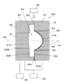
- the molding die 100 forms a mold space CV by clamping a fixed die 10 as a first die and a movable die 20 as a second die to form a plastic lens PL as an optical element (see FIG. 3). ).
- the molding die 100 is incorporated into an injection molding apparatus including the temperature adjusting unit 30, the movable mold driving unit 40, the resin injection unit 50, and the like.
- the molding die 100 includes a fixed die 10 and a movable die 20.
- a mold space CV is formed between the molds 10 and 20 by abutting the movable mold 20 against the fixed mold 10.
- a gate GP communicating with the mold space CV is formed in a part of the periphery of the mold space CV.
- the mold space CV is filled with molten resin by the resin injection unit 50 through the gate GP.
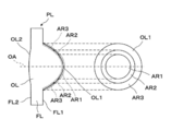
- the plastic lens PL molded by the molding die 100 will be described.
- the left side is a side sectional view of the plastic lens PL
- the right side is a conceptual diagram of the first optical surface OL1.
- the plastic lens PL is a small diffractive refractive compound lens, and is used as an objective lens of an optical pickup device, for example.
- the plastic lens PL has a center portion OL having an optical function and an annular flange portion FL extending from the center portion OL in the outer diameter direction.
- the center portion OL has a convex first optical surface OL1 having a small curvature radius and a convex second optical surface OL2 having a large curvature radius.
- the first optical surface OL1 and the second optical surface OL2 are opposed to each other with a thick and light-transmitting main body interposed therebetween.
- the flange portion FL has a first flange surface FL1 on the first optical surface OL1 side and a second flange surface FL2 on the second optical surface OL2 side.
- the first optical surface OL1 has a step of the diffractive structure, that is, a fine structure in order to be compatible with multiple wavelengths. That is, the plastic lens PL is a three-wavelength compatible optical element corresponding to a short wavelength, high numerical aperture standard, a medium wavelength, medium numerical aperture standard, and a long wavelength, low numerical aperture standard.
- the fine structure provided on one optical surface OL1 has a shape that allows light collection in conformity with each wavelength.
- the first optical surface OL1 is divided into three concentric regions to correspond to light beams of three wavelengths having different numerical apertures, and a three-wavelength compatible region AR1 and two wavelengths from the inside toward the outside.
- the compatible area AR2 and the one-wavelength dedicated area AR3 are included. With all these areas AR1, AR2, AR3, for example, the wavelength (405 nm) of BD (Blu-ray Disc) is condensed with a numerical aperture (NA) of 0.85, and an optimal spot is formed on the BD optical disk. Further, by using the areas AR1 and AR2 excluding the outermost peripheral side away from the optical axis OA, for example, the wavelength (650 nm) of DVD (Digital Versatile Disc) is condensed with a numerical aperture (NA) of 0.6, and the optical disc on the DVD is collected. To form the optimal spot.
- BD Blu-ray Disc
- NA numerical aperture
- the light flux of DVD wavelength (650 nm) that passes through the optical surface area corresponding to NA 0.6 to NA 0.85 is a flare component that does not contribute to the formation of spots used for recording / reproduction of DVD optical discs.
- a wavelength (780 nm) of CD Compact Disc
- NA numerical aperture
- the light flux of the CD wavelength (780 nm) passing through the region of the optical surface corresponding to NA 0.45 to NA 0.85 is a flare component that does not contribute to the formation of spots used for recording / reproduction of CD optical discs.
- the specific fine structure of the first optical surface OL1 is a transfer of the fine structure of the first optical transfer surface 11A of the fixed mold 10, which will be described later, and will not be described.
- the fixed mold 10 has a core mold 11 on the center side and an outer peripheral mold 12 on the peripheral side.
- the core mold 11 and the outer peripheral mold 12 are formed of the same steel material, for example, and are integrally fixed to each other.
- the core mold 11 is provided with a ring-shaped diffraction pattern having a fine structure on the side facing the movable mold 20, and has a first optical transfer surface 11 ⁇ / b> A that is concave as a whole.
- the first molding surface 12A on the peripheral side formed by the outer peripheral mold 12 corresponds to the first flange surface FL1 (see FIG. 3) around the plastic lens PL.
- FIG. 2 is a schematic enlarged view of a side cross section of the first optical transfer surface 11A.
- the surface formed by the first optical transfer surface 11A is the first optical surface OL1 of the plastic lens PL.
- the first optical transfer surface 11A has a circular optical axis side region 11C and a ring-shaped outer region 11D so as to be concentric from the optical axis OA side of the first optical transfer surface 11A toward the outer side in the radial direction. Divided.
- the optical axis side region 11C is further divided into a concentric central region A1 and intermediate region A2 from the center of the first optical transfer surface 11A toward the outer region 11D.
- the center area A1 corresponds to the three-wavelength compatible area AR1 of the plastic lens PL of FIG. 3, and the intermediate area A2 corresponds to the two-wavelength compatible area AR2.
- the outer region 11D is the outermost peripheral region A3 and corresponds to the one-wavelength dedicated region AR3 of the plastic lens PL of FIG.
- a large number of fine step shapes form the optical axis OA in each of the central region A1, the intermediate region A2, and the outermost peripheral region A3. It is formed in a ring shape at the center.
- this ring-shaped step shape is viewed as a cross section, the inner wall surface of the concave step shape that causes mold release resistance is parallel to the optical axis OA, and the inner wall surface of the step shape and the optical axis OA are The angles ⁇ 1 and ⁇ 3 formed are respectively equal to or less than the angles ⁇ 1 and ⁇ 3 formed by the outer wall surface of the step shape and the optical axis OA.
- the step shape 13A in the central region A1 of the first optical transfer surface 11A, is rectangular, and the inner wall surface 13B of all the step shapes 13A in the region and the optical axis OA. And the angle ⁇ 1 formed by the outer wall surface 13C of the step shape 13A and the optical axis OA are both 0 degrees and the same. In the most peripheral area A3, the step shape 15A is blazed.
- the angle ⁇ 3 formed by the outer wall surface 15C of each step shape 15A and the optical axis OA may have different values.
- the angle ⁇ 1 (the angle ⁇ 2 is also the same between the outer wall surfaces and the optical axis OA).
- the angle ⁇ 3 formed by the inner wall surface 15B and the optical axis OA is smaller than the angle ⁇ 3 formed by the outer wall surface 15C and the optical axis OA.
- the minimum value of the angle ⁇ 3 formed by the outer wall surface 15C of the step shape 15A and the optical axis OA in the outermost region A3 of the outer region 11D is the central region A1 in the optical axis side region 11C. It is larger than the angle ⁇ 1 formed by the outer wall surface 13C of the step shape 13A and the optical axis OA.
- region A2 is rectangular shape, for example, and the angle which the wall surface inside the level
- Is equal to or smaller than the angle formed by the outer wall surface and the optical axis OA, for example, they are equal to each other.
- the minimum value of the angle ⁇ 3 formed by the outer wall surface of the step shape 15A in the most peripheral area A3 and the optical axis OA is larger than the angle formed by the outer wall surface of the step shape in the intermediate area A2 and the optical axis OA. .
- the width of the step shape is X
- the height of the step shape is Y
- the aspect ratio value (Y / X) of the step shape is the following conditional expression 0.50 ⁇ ( Maximum value of Y / X) ⁇ 1.0
- the step shape of the first optical transfer surface 11A is relatively deep.
- Such an optical transfer surface having a relatively deep step shape is indispensable for forming a multi-wavelength compatible optical element, specifically, a three-wavelength compatible optical element.
- the maximum value of the aspect ratio (Y / X) between the width X and the height Y of the step shape in each of the regions 11C and 11D is the maximum value when the step shape has a U-shaped step shape.
- the maximum value of (Y / X) is obtained on the basis of the ratio between the width X1 and the height Y1 of the U-shaped step shape UN1.
- the height Y1 of the U-shaped step shape UN1 is, as shown in FIG. 2, the optical axis OA direction of two wall surfaces parallel to the optical axis OA forming the U-shaped step shape UN1.
- the height of the wall surface having the higher height is Y1.
- the step shape is obtained based on the value of the ratio between the width X and the height Y of the blaze type step shape. For example, as shown in FIG. 2, in the most peripheral area A3, the maximum value of (Y / X) is obtained based on the ratio of the width X3 and the height Y3 of the blaze-shaped step shape UN3.
- the step shapes in the regions 11C and 11D are different from each other, and the maximum value of (Y / X) in the outermost peripheral region A3 which is the outer region 11D is It is smaller than the maximum value of (Y / X) in the central region A1 of the optical axis side region 11C.
- the step shape in the intermediate area A2 is, for example, a rectangle, and the maximum value of (Y / X) in the intermediate area A2 is (Y / X) in the most peripheral area A3 in the specific example. It is larger than the maximum value.
- a step is formed by substantially inverting the step shapes 13A, 15A formed in each of the areas A1, A3, etc. of the first optical transfer surface 11A.
- the movable mold 20 has a core mold 21 on the center side and an outer peripheral mold 22 on the peripheral side.
- the core mold 21 and the outer peripheral mold 22 are made of, for example, the same steel material, and the outer peripheral mold 22 supports the core mold 21 from the periphery.
- the core mold 21 has a smooth concave second optical transfer surface 21 ⁇ / b> A having no step on the side facing the fixed mold 10.
- the second optical transfer surface 21A corresponds to the second optical surface OL2 (see FIG. 3) having a large curvature radius of the plastic lens PL that is a molded product.
- the second molding surface 22A on the peripheral side formed by the outer peripheral die 22 corresponds to the second flange surface FL2 (see FIG. 3) around the plastic lens PL.
- the core mold 21 functions as a protruding portion, and can reciprocate in the direction of the axis AX while being inserted slightly through a hole 22B provided in the outer peripheral mold 22. After the mold is opened to move the movable mold 20 away from the fixed mold 10, the core mold 21 is moved toward the fixed mold 10 with respect to the outer peripheral mold 22, thereby easily releasing the plastic lens PL remaining on the movable mold 20. Can do.
- the mold is closed by joining the movable mold 20 to the fixed mold 10.
- a mold space CV having a shape in which the parting line surface PA1 of the fixed mold 10 and the parting line surface PA2 of the movable mold 20 are closed is formed between the molds 10 and 20.
- molten plastic resin is injected into a mold space CV formed between both molds 10 and 20. That is, the molten plastic resin is introduced into the mold space CV between the molds 10 and 20 through the gate GP, and the mold space CV is filled with the molten plastic resin.
- the molten plastic resin filled in the mold space CV is radiated and cooled.
- the temperature of the molten plastic resin injected into the mold space CV is usually 200 to 300 ° C., and the optical transfer surfaces 11 A and 21 A of both molds 10 and 20 held by the temperature adjusting unit 30 at a normal temperature of 100 to 180 ° C. And when it contacts the molding surfaces 12A and 22A, the molten plastic resin gradually cools and solidifies from the contact surface with the molding die 100.
- mold opening is performed to separate the movable mold 20 from the fixed mold 10 while the molten plastic resin is warm. Thereby, the mold release resistance due to the resin shrinkage due to cooling and solidification is suppressed, and even if the first optical transfer surface 11A of the molding die 100 has a relatively deep step shape, the first optical surface of the plastic lens PL. OL1 is smoothly released from the fixed mold 10 with almost no resistance.
- the mold opening distance for moving the movable mold 20 backward is, for example, about the thickness of the diffraction lens.
- the core mold 21 that is a protruding part is moved from the illustrated retracted state housed in the outer peripheral mold 22 to the fixed mold 10 side to the fixed mold 10 side from the second molding surface 22A.
- the plastic lens PL in which the resin contraction due to cooling is remarkable can be released from the movable mold 20, that is, separated.
- the first optical surface OL1 is a convex surface having an annular diffraction pattern corresponding to the first optical transfer surface 11A
- the second optical surface OL2 has a smooth convex surface corresponding to the second optical transfer surface 21A.
- a flange portion FL is formed corresponding to the molding surfaces 12A and 22A.
- the molding die 100 described above by separating the first optical transfer surface 11A having the step shapes 13A and 15A forming the diffractive structure from the plastic lens PL before the second optical transfer surface 21A, For example, even if the stepped shapes 13A and 15A such as a three-wavelength compatible optical element are in a relatively deep range satisfying the maximum value ⁇ 1.0 of 0.50 ⁇ (Y / X), the resin by cooling and solidifying at the time of injection molding Release resistance due to shrinkage can be suppressed. Thereby, the plastic lens PL is released from the fixed mold 10 smoothly without any resistance, and the step of the diffractive structure of the plastic lens PL, that is, the deformation of the fine shape can be prevented.
- the stepped shapes 13A and 15A such as a three-wavelength compatible optical element
- the maximum value of (Y / X) in the outermost region A3 of the outer region 11D is made smaller than the maximum value of (Y / X) in the central region A1 of the optical axis side region 11C, etc.
- the mold release resistance applied to the inner wall surface 15B of the step shape 15A in the most peripheral area A3 can be relaxed, and the mold can be more easily released from the fixed mold 10 even if the plastic lens PL is cooled and solidified from the outside.
- the minimum value of the angle ⁇ 3 formed by the outer wall surface 15C of the step shape 15A and the optical axis OA in the outermost region A3 of the outer region 11D is the outer wall surface of the step shape 13A in the central region A1 of the optical axis side region 11C.
- the step shape 15A in the most peripheral region A3 has less mold release resistance due to resin contraction than the step shape 13A in the central region A1, and the plastic Even if the lens PL is cooled and solidified from the outside, it can be easily released from the fixed mold 10.
- Table 1 explains the aspect ratio value (Y / X) of the step shape on the first optical transfer surface 11A of FIG.
- the aspect ratio value (Y1 / X1) of the step shape UN1 in the central region A1 is 0.038 to 0.617.
- the aspect ratio value (Y3 / X3) of the step shape UN3 in the most peripheral area A3 is 0.005 to 0.030.
- the maximum value of (Y / X) in the central area A1 is 0.617
- the maximum value of (Y / X) in the most peripheral area A3 is 0.030.
- the maximum value of the aspect ratio (Y / X) of the step shape is 0.617, and the maximum value of 0.50 ⁇ (Y / X) ⁇ 1. Within the range of 0.0.
- the maximum value (0.030) of (Y / X) in the outermost region A3 of the outer region 11D is greater than the maximum value (0.617) of (Y / X) in the central region A1 of the optical axis side region 11C. Is also getting smaller.
- the molding die according to the second embodiment is a modification of the molding die according to the first embodiment, and portions not particularly described are the same as those in the first embodiment.
- a large number of fine step shapes for forming the steps of the diffractive structure of the plastic lens PL are formed in an annular shape around the optical axis OA.
- this ring-shaped step shape is viewed as a cross section, the inner wall surface of the concave step shape that causes mold release resistance is parallel to the optical axis OA, and the inner wall surface of the step shape and the optical axis OA are The angles ⁇ 1, ⁇ 2, and ⁇ 3 formed are equal to or less than the angles ⁇ 1, ⁇ 2, and ⁇ 3 formed by the outer wall surface of the step shape and the optical axis OA, respectively.
- the step shape 13A in the central region A1 of the first optical transfer surface 11A, is rectangular, and the inner wall surface 13B of all the step shapes 13A in the region and the optical axis OA. And the angle ⁇ 1 formed by the outer wall surface 13C of the step shape 13A and the optical axis OA are both 0 degrees and the same.
- the step shape 14A in the intermediate region A2, is rectangular, and an angle ⁇ 2 formed by the inner wall surface 14B of all the step shapes 14A in the region and the optical axis OA, and the outer wall surface 14C of the step shape 14A
- the angle ⁇ 2 formed by the optical axis OA is 0 degree and is the same.
- the step shape 15A is blazed, and in each step shape 15A, the angle ⁇ 3 formed by the inner wall surface 15B and the optical axis OA is equal to the outer wall surface 15C and the optical axis OA. Is smaller than the angle ⁇ 3 formed by.
- the minimum value of the angle ⁇ 3 formed by the outer wall surface 15C of the step shape 15A and the optical axis OA in the outermost region A3 of the outer region 11D is the central region A1 in the optical axis side region 11C. It is larger than the angle ⁇ 1 formed by the outer wall surface 13C of the stepped shape 13A and the optical axis OA and the similar angle ⁇ 2 in the intermediate region A2.
- the width of the step shape is X
- the height of the step shape is Y
- the aspect ratio value (Y / X) of the step shape is the following conditional expression 0.50 ⁇ ( Maximum value of Y / X) ⁇ 1.0
- the step shape of the first optical transfer surface 11A is relatively deep.
- the maximum value of the aspect ratio (Y / X) between the width X and the height Y of the step shape in each of the regions 11C and 11D is the maximum value when the step shape has a U-shaped step shape. It is obtained on the basis of the value of the ratio between the width X and the height Y of the U-shaped step shape. For example, as shown in FIG.
- the maximum value of (Y / X) is obtained on the basis of the ratio between the width X1 and the height Y1 of the U-shaped step shape UN1.
- the height Y1 of the U-shaped step shape UN1 is the direction of the optical axis OA among two wall surfaces parallel to the optical axis OA forming the U-shaped step shape UN1.
- the height of the wall surface having the higher height is Y1.
- the maximum value of (Y / X) is obtained based on the ratio of the width X2 and the height Y2 of the U-shaped step shape UN2.
- the height Y2 of the U-shaped step shape UN2 is, as shown in FIG.
- the height of the wall with the higher height is Y2.
- the step shape is obtained based on the value of the ratio between the width X and the height Y of the blaze type step shape. For example, as shown in FIG. 4, in the most peripheral area A3, the maximum value of (Y / X) is obtained based on the ratio between the width X3 and the height Y3 of the blaze-shaped step shape UN3.
- the step shapes in the regions 11C and 11D, specifically the regions A1, A2 and A3, are different from each other, and the maximum value of (Y / X) in the outermost region A3 of the outer region 11D is the optical axis side. It is smaller than the maximum value of (Y / X) in either one of the central region A1 and the intermediate region A2 of the region 11C.
- steps formed by substantially inverting the step shapes 13A, 14A, 15A formed in the areas A1, A2, A3 of the first optical transfer surface 11A are formed. Is done.
- the minimum value of the angle ⁇ 3 formed by the outer wall surface 15C of the step shape 15A and the optical axis OA in the outermost peripheral region A3 of the outer region 11D is determined as the central region of the optical axis side region 11C.
- the step shape 15A in the outermost peripheral region A3 is changed from the central region A1 and the intermediate region A3 by increasing the angle ⁇ 1, ⁇ 2 between the outer wall surfaces 13C, 14C of the step shape 13A, 14A in the intermediate region A2 and the optical axis OA.
- the mold release resistance due to resin contraction is smaller than the step shapes 13A and 14A in the region A2, and even when the plastic lens PL is cooled and solidified from the outside, it can be easily released from the fixed mold 10.
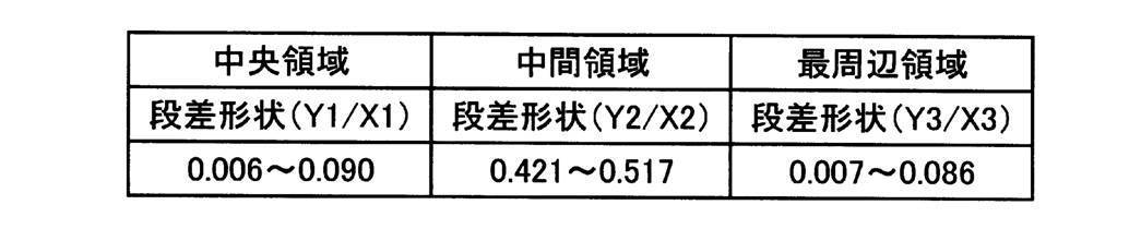
- Table 2 explains the aspect ratio value (Y / X) of the step shape on the first optical transfer surface 11A of FIG.
- the aspect ratio value (Y1 / X1) of the step shape UN1 in the central area A1 is 0.006 to 0.090
- the aspect ratio value of the step shape UN2 in the intermediate area A2 (Y2 / X2) is 0.421 to 0.517
- the aspect ratio value (Y3 / X3) of the step shape UN3 in the most peripheral area A3 is 0.007 to 0.086.
- the maximum value of (Y / X) in the central area A1 is 0.090
- the maximum value of (Y / X) in the intermediate area A2 is 0.517
- the maximum value is 0.086.
- the maximum value of the aspect ratio (Y / X) of the step shape is 0.517, and the maximum value of 0.50 ⁇ (Y / X) ⁇ 1. Within the range of 0.0. Further, the maximum value (0.086) of (Y / X) in the outermost peripheral region A3 of the outer region 11D is the maximum value (0.090) of (Y / X) in the central region A1 of the optical axis side region 11C. And, it is smaller than the maximum value (0.517) of (Y / X) in the intermediate region A2 of the optical axis side region 11C.
- the molding die of the third embodiment is a modification of the molding die of the first embodiment, and the parts that are not particularly described are the same as those of the first embodiment.
- a large number of fine step shapes for forming the steps of the diffractive structure of the plastic lens PL are formed in an annular shape around the optical axis OA.
- this ring-shaped step shape is viewed as a cross section, the inner wall surface of the concave step shape that causes mold release resistance is parallel to the optical axis OA, and the inner wall surface of the step shape and the optical axis OA are The angles ⁇ 1, ⁇ 2, and ⁇ 3 formed are equal to or less than the angles ⁇ 1, ⁇ 2, and ⁇ 3 formed by the outer wall surface of the step shape and the optical axis OA, respectively.
- the step shape 13A in the central region A1 of the first optical transfer surface 11A, is rectangular, and the angle ⁇ 1 formed by the inner wall surface 13B of the step shape 13A and the optical axis OA.
- the angle ⁇ 1 formed by the outer wall surface 13C of the step shape 13A and the optical axis OA is both 0 degrees and the same.
- the step shape 14A is blazed.
- the angle ⁇ 2 formed between the inner wall surface 14B and the optical axis OA is determined by the outer wall surface 14C and the optical axis OA. It is smaller than the formed angle ⁇ 2.
- the step shape 15A is blazed, and in each step shape 15A, the angle ⁇ 3 formed by the inner wall surface 15B and the optical axis OA is equal to the outer wall surface 15C and the optical axis OA. Is smaller than the angle ⁇ 3 formed by.
- the minimum value of the angle ⁇ 3 formed by the outer wall surface 15C of the step shape 15A and the optical axis OA in the outermost region A3 of the outer region 11D is the central region A1 in the optical axis side region 11C.
- the angle formed by the outer wall surface 14C of the step shape 14A and the optical axis OA in the intermediate region A2 of the optical axis side region 11C is larger than the angle ⁇ 1 formed by the outer wall surface 13C of the step shape 13A and the optical axis OA. It is smaller than the minimum value of ⁇ 2.
- the width of the step shape is X
- the height of the step shape is Y
- the aspect ratio value (Y / X) of the step shape is the following conditional expression 0.50 ⁇ ( Maximum value of Y / X) ⁇ 1.0
- the step shape of the first optical transfer surface 11A is relatively deep.
- the maximum value of the aspect ratio (Y / X) between the width X and the height Y of the step shape in each of the regions 11C and 11D is the maximum value when the step shape has a U-shaped step shape. It is obtained on the basis of the value of the ratio between the width X and the height Y of the U-shaped step shape. For example, as shown in FIG.
- the maximum value of (Y / X) is obtained based on the ratio of the width X1 and the height Y1 of the U-shaped step shape UN1.
- the height Y1 of the U-shaped step shape UN1 is the direction of the optical axis OA among the two wall surfaces parallel to the optical axis OA forming the U-shaped step shape UN1.
- the height of the wall surface having the higher height is Y1.
- the maximum value of (Y / X) is obtained on the basis of the ratio between the width X2 and the height Y2 of the blaze-shaped step shape UN2.
- the maximum value of (Y / X) is obtained based on the ratio between the width X3 and the height Y3 of the blaze-shaped step shape UN3.
- the step shapes in the regions 11C and 11D, specifically the regions A1, A2 and A3, are different from each other, and the maximum value of (Y / X) in the outermost region A3 of the outer region 11D is the optical axis side. It is smaller than the maximum value of (Y / X) in either one of the central region A1 and the intermediate region A2 of the region 11C.
- steps formed by substantially inverting the step shapes 13A, 14A, 15A formed in the areas A1, A2, A3 of the first optical transfer surface 11A are formed. Is done.
- the minimum value of the angle ⁇ 3 formed by the outer wall surface 15C of the step shape 15A and the optical axis OA in the outermost peripheral region A3 of the outer region 11D is determined as the central region of the optical axis side region 11C.
- the step shape 15A in the outermost peripheral area A3 is released by contraction of the resin more than the step shape 13A in the central area A1 by making it larger than the angle ⁇ 1 formed by the outer wall surface 13C of the step shape 13A in A1 and the optical axis OA. Even if the resistance is reduced and the plastic lens PL is cooled and solidified from the outside, it can be easily released from the fixed mold 10.
- Table 3 explains the aspect ratio value (Y / X) of the step shape on the first optical transfer surface 11A of FIG.
- the aspect ratio value (Y1 / X1) of the step shape UN1 in the central region A1 is 0.110 to 0.957
- the aspect ratio value of the step shape UN2 in the intermediate region A2 (Y2 / X2) is 0.039 to 0.112.
- the aspect ratio value (Y3 / X3) of the step shape UN3 in the most peripheral area A3 is 0.064 to 0.362.
- the maximum value of (Y / X) in the central area A1 is 0.957
- the maximum value of (Y / X) in the intermediate area A2 is 0.112
- the maximum value is 0.362.
- the maximum value of the aspect ratio (Y / X) of the step shape is 0.957, and the maximum value of 0.50 ⁇ (Y / X) ⁇ 1. Within the range of 0.0.
- the maximum value (0.362) of (Y / X) in the outermost region A3 of the outer region 11D is larger than the maximum value (0.957) of (Y / X) in the central region A1 of the optical axis side region 11C. Is also getting smaller.
- the molding die according to the fourth embodiment is a modification of the molding die according to the first embodiment, and portions not particularly described are the same as those in the first embodiment.
- a large number of fine step shapes for forming the steps of the diffractive structure of the plastic lens PL are formed in an annular shape around the optical axis OA.
- this ring-shaped step shape is viewed as a cross section, the inner wall surface of the concave step shape that causes mold release resistance is parallel to the optical axis OA, and the inner wall surface of the step shape and the optical axis OA are The angles ⁇ 1 and ⁇ 3 formed are respectively equal to or less than the angles ⁇ 1 and ⁇ 3 formed by the outer wall surface of the step shape and the optical axis OA.
- the step shape 13A is a blazed shape, and the inner wall surface 13B and the optical axis OA are in each step shape 13A.
- the angle ⁇ 1 formed is smaller than the angle ⁇ 1 formed by the outer wall surface 13C and the optical axis OA.
- the step shape 15A is rectangular, and the angle ⁇ 3 formed by the inner wall surface 15B and the optical axis OA in all the step shapes 15A is 0 degree.
- the angle ⁇ 3 formed by the outer wall surface 15C of the step shape 15A and the optical axis OA can take a plurality of different values of 0 degrees or more corresponding to the angle of the base aspheric surface (base surface). That is, the inner angle ⁇ 1 is equal to or smaller than the outer angle ⁇ 3.
- the minimum value of the angle ⁇ 3 formed by the outer wall surface 15C of the step shape 15A and the optical axis OA in the outermost peripheral region A3 of the outer region 11D is the central region A1 in the optical axis side region 11C. Is smaller than the minimum value of the angle ⁇ 1 formed by the outer wall surface 13C of the step shape 13A and the optical axis OA.
- the step shape in the intermediate region A2 is, for example, a blazed shape, and the angle formed between the inner wall surface and the optical axis OA in each step shape in the intermediate region A2 is the outer wall surface. And the angle formed by the optical axis OA.
- the minimum value of the angle ⁇ 3 formed by the outer wall surface of the step shape 15A in the most peripheral area A3 and the optical axis OA is smaller than the minimum value of the angle formed by the outer wall surface of the step shape in the intermediate area A2 and the optical axis OA. It has become.
- the width of the step shape is X
- the height of the step shape is Y
- the aspect ratio value (Y / X) of the step shape is the following conditional expression 0.50 ⁇ ( Maximum value of Y / X) ⁇ 1.0
- the step shape of the first optical transfer surface 11A is relatively deep.
- the maximum value of the aspect ratio (Y / X) between the width X and the height Y of the step shape in each of the regions 11C and 11D is the maximum value when the step shape has a U-shaped step shape. It is obtained on the basis of the value of the ratio between the width X and the height Y of the U-shaped step shape. For example, as shown in FIG.
- the maximum value of (Y / X) is obtained based on the ratio of the width X3 and the height Y3 of the U-shaped step shape UN3.
- the height Y3 of the U-shaped step shape UN3 is, as shown in FIG. 6, the direction of the optical axis OA among the two wall surfaces parallel to the optical axis OA forming the U-shaped step shape UN3.
- the height of the wall surface having the higher height is Y3.
- the step shape does not have a U-shaped step shape, for example, in the case of a blaze type step shape, the step shape is obtained based on the value of the ratio between the width X and the height Y of the blaze type step shape.
- the maximum value of (Y / X) is obtained on the basis of the ratio between the width X1 and the height Y1 of the blaze-type step shape UN1.
- the step shapes in the regions 11C and 11D are different from each other, and the maximum value of (Y / X) in the outermost peripheral region A3 of the outer region 11D. Is smaller than the maximum value of (Y / X) in the central region A1 of the optical axis side region 11C.
- the step shape in the intermediate area A2 is, for example, a rectangle, and the maximum value of (Y / X) in the intermediate area A2 is (Y / X) in the most peripheral area A3 in the specific example. It is larger than the maximum value.
- a step is formed by substantially inverting the step shapes 13A, 15A formed in each of the areas A1, A3, etc. of the first optical transfer surface 11A.
- the minimum value of the angle ⁇ 3 formed by the outer wall surface 15C of the step shape 15A and the optical axis OA in the outermost peripheral region A3 of the outer region 11D is the central region of the optical axis side region 11C.
- the mold structure is such that the mold release resistance tends to be relatively large on the outside, which is smaller than the minimum value of the angle ⁇ 1 formed by the outer wall surface 13C of the step shape 13A in A1 and the optical axis OA, but the mold release resistance is large.
- the step shape 13A of the central region A1 may be rectangular.
- the minimum value of the angle ⁇ 3 formed by the outer wall surface 15C of the step shape 15A in the outermost region A3 of the outer region 11D and the optical axis OA is outside the step shape 13A in the central region A1 of the optical axis side region 11C. It becomes 0 degree which is the same as the angle ⁇ 1 formed by the wall surface 13C of the optical axis OA.
- the molding die according to the present embodiment has been described above, but the molding die according to the present invention is not limited to the above.
- the plastic lens PL remaining on the movable mold 20 is released by protruding the core mold 21, but the second flange surface FL2 of the plastic lens PL by the protruding pin embedded in the movable mold 20 is used. May protrude from the movable mold 20.
- the shapes of the step shapes 13A, 14A, and 15A are examples, and combinations of shapes can be freely designed within the range of conditions.
- the same or similar pattern can be formed in the central area A1 and the intermediate area A2 constituting the optical axis side area 11C.
- all the step shapes in the central area A1, the intermediate area A2, and the most peripheral area may be rectangular or blazed.
Landscapes
- Engineering & Computer Science (AREA)
- Manufacturing & Machinery (AREA)
- Mechanical Engineering (AREA)
- Health & Medical Sciences (AREA)
- Ophthalmology & Optometry (AREA)
- Moulds For Moulding Plastics Or The Like (AREA)
- Diffracting Gratings Or Hologram Optical Elements (AREA)
- Lenses (AREA)
Abstract
Description
0.50≦(Y/X)の最大値≦1.0
を満たすことを特徴とする。ここで、(Y/X)は、段差形状の幅と高さの比の値である。
0.50≦(Y/X)の最大値≦1.0
を満たすことを特徴とする。
0.50≦(Y/X)の最大値≦1.0
を満たし、型開き工程の後、第2金型から光学素子を離型させる離型工程を有することを特徴とする。
図1及び図2を参照して、本発明の成形金型について説明する。成形金型100は、第1金型である固定型10と第2金型である可動型20とを型締めすることによって型空間CVを形成して光学素子であるプラスチックレンズPL(図3参照)の成形を行うものである。成形金型100は、温度調節部30、可動型駆動部40、樹脂射出部50等を備える射出成形装置に組み込まれる。
0.50≦(Y/X)の最大値≦1.0
を満たすようになっており、第1光学転写面11Aの段差形状が比較的深いものとなっている。このような段差形状が比較的深い光学転写面は、多波長互換光学素子、具体的には3波長互換光学素子の形成に不可欠的になっている。ここで、各領域11C,11Dにおける段差形状の幅Xと高さYとの縦横比の値(Y/X)の最大値は、段差形状がコの字型の段差形状を有する場合は、コの字型の段差形状の幅Xと高さYの比の値を基準にして求める。例えば、図2に示すように、中央領域A1において、コの字型の段差形状UN1の幅X1と高さY1との比を基準にして(Y/X)の最大値を求める。なお、コの字型の段差形状UN1の高さY1は、図2に示すように、コの字型の段差形状UN1を形成する光軸OAに平行な2つの壁面のうち、光軸OA方向の高さが高い方の壁面の高さをY1としている。段差形状がコの字型の段差形状を有していない場合、例えばブレーズ型の段差形状の場合は、ブレーズ型の段差形状の幅Xと高さYの比の値を基準にして求める。例えば、図2に示すように、最周辺領域A3において、ブレーズ型の段差形状UN3の幅X3と高さY3との比を基準にして(Y/X)の最大値を求める。

以下、本発明に係る第2実施形態の成形金型について説明する。第2実施形態の成形金型は、第1実施形態の成形金型を変形したものであり、特に説明しない部分は、第1実施形態と同様である。
0.50≦(Y/X)の最大値≦1.0
を満たすようになっており、第1光学転写面11Aの段差形状が比較的深いものとなっている。ここで、各領域11C,11Dにおける段差形状の幅Xと高さYとの縦横比の値(Y/X)の最大値は、段差形状がコの字型の段差形状を有する場合は、コの字型の段差形状の幅Xと高さYの比の値を基準にして求める。例えば、図4に示すように、中央領域A1において、コの字型の段差形状UN1の幅X1と高さY1との比を基準にして(Y/X)の最大値を求める。なお、コの字型の段差形状UN1の高さY1は、図4に示すように、コの字型の段差形状UN1を形成する光軸OAに平行な2つの壁面のうち、光軸OA方向の高さが高い方の壁面の高さをY1としている。また、中間領域A2において、コの字型の段差形状UN2の幅X2と高さY2との比を基準にして(Y/X)の最大値を求める。なお、コの字型の段差形状UN2の高さY2は、図4に示すように、コの字型の段差形状UN2を形成する光軸OAに平行な2つの壁面のうち、光軸OA方向の高さが高い方の壁面の高さをY2としている。段差形状がコの字型の段差形状を有していない場合、例えばブレーズ型の段差形状の場合は、ブレーズ型の段差形状の幅Xと高さYの比の値を基準にして求める。例えば、図4に示すように、最周辺領域A3において、ブレーズ型の段差形状UN3の幅X3と高さY3との比を基準にして(Y/X)の最大値を求める。
以下、本発明に係る第3実施形態の成形金型について説明する。第3実施形態の成形金型は、第1実施形態の成形金型を変形したものであり、特に説明しない部分は、第1実施形態と同様である。
0.50≦(Y/X)の最大値≦1.0
を満たすようになっており、第1光学転写面11Aの段差形状が比較的深いものとなっている。ここで、各領域11C,11Dにおける段差形状の幅Xと高さYとの縦横比の値(Y/X)の最大値は、段差形状がコの字型の段差形状を有する場合は、コの字型の段差形状の幅Xと高さYの比の値を基準にして求める。例えば、図5に示すように、中央領域A1において、コの字型の段差形状UN1の幅X1と高さY1との比を基準にして(Y/X)の最大値を求める。なお、コの字型の段差形状UN1の高さY1は、図5に示すように、コの字型の段差形状UN1を形成する光軸OAに平行な2つの壁面のうち、光軸OA方向の高さが高い方の壁面の高さをY1としている。段差形状がコの字型の段差形状を有していない場合、例えばブレーズ型の段差形状の場合は、ブレーズ型の段差形状の幅Xと高さYの比の値を基準にして求める。例えば、図5に示すように、中間領域A2において、ブレーズ型の段差形状UN2の幅X2と高さY2との比を基準にして(Y/X)の最大値を求める。また、最周辺領域A3において、ブレーズ型の段差形状UN3の幅X3と高さY3との比を基準にして(Y/X)の最大値を求める。

以下、本発明に係る第4実施形態の成形金型について説明する。第4実施形態の成形金型は、第1実施形態の成形金型を変形したものであり、特に説明しない部分は、第1実施形態と同様である。
0.50≦(Y/X)の最大値≦1.0
を満たすようになっており、第1光学転写面11Aの段差形状が比較的深いものとなっている。ここで、各領域11C,11Dにおける段差形状の幅Xと高さYとの縦横比の値(Y/X)の最大値は、段差形状がコの字型の段差形状を有する場合は、コの字型の段差形状の幅Xと高さYの比の値を基準にして求める。例えば、図6に示すように、最周辺領域A3において、コの字型の段差形状UN3の幅X3と高さY3との比を基準にして(Y/X)の最大値を求める。なお、コの字型の段差形状UN3の高さY3は、図6に示すように、コの字型の段差形状UN3を形成する光軸OAに平行な2つの壁面のうち、光軸OA方向の高さが高い方の壁面の高さをY3としている。段差形状がコの字型の段差形状を有していない場合、例えばブレーズ型の段差形状の場合は、ブレーズ型の段差形状の幅Xと高さYの比の値を基準にして求める。例えば、図6に示すように、中央領域A1において、ブレーズ型の段差形状UN1の幅X1と高さY1との比を基準にして(Y/X)の最大値を求める。
10 固定型
20 可動型
30 温度調節部
40 可動型駆動部
50 樹脂射出部
11A,21A 光学転写面
11C 光軸側領域
11D 外側領域
12A,22A 成形面
13A,14A,15A 段差形状
A1 中央領域
A2 中間領域
A3 最周辺領域
CV 型空間
OL 中心部
OL1,OL2 光学面
FL フランジ部
FL1,FL2 フランジ面
PL プラスチックレンズ
OA 光軸
Claims (18)
- 第1金型と第2金型とを型締めすることによって型空間を形成して光学素子の成形を行う成形金型であって、
前記第1金型は、前記光学素子の第1光学面を形成する第1光学転写面を有し、前記第2金型よりも先に前記光学素子から離型し、
前記第2金型は、前記光学素子の第2光学面を形成する第2光学転写面を有し、前記第1金型の離型の際に前記光学素子を保持し、
前記第1光学転写面の曲率半径の絶対値は、前記第2光学転写面の曲率半径の絶対値よりも小さく、
前記第1光学転写面は、回折構造を形成する段差形状を有し、
前記段差形状の幅をXとし、前記段差形状の高さをYとして、以下の条件式
0.50≦(Y/X)の最大値≦1.0
を満たすことを特徴とする成形金型。 - 前記第1光学転写面は、光軸側に配置される光軸側領域と、前記光軸側領域よりも外側に配置される外側領域とを少なくとも有し、
前記外側領域における前記(Y/X)の最大値は、前記光軸側領域における前記(Y/X)の最大値よりも小さいことを特徴とする請求項1に記載の成形金型。 - 前記段差形状の内側の壁面と光軸とがなす角度は、前記段差形状の外側の壁面と光軸とがなす角度以下であることを特徴とする請求項1及び請求項2のいずれか一項に記載の成形金型。
- 前記段差形状の内側の壁面は、光軸に平行であることを特徴とする請求項1から請求項3までのいずれか一項に記載の成形金型。
- 前記段差形状は、矩形状を含むことを特徴とする請求項1から請求項4までのいずれか一項に記載の成形金型。
- 前記外側領域における段差形状の外側の壁面と光軸とがなす角度の最小値は、前記光軸側領域における段差形状の外側の壁面と光軸とがなす角度の最小値よりも大きいことを特徴とする請求項2から請求項5までのいずれか一項に記載の成形金型。
- 前記光軸側領域は、光軸側に配置される中央領域と、前記中央領域よりも外側に配置される中間領域とを少なくとも有し、
前記外側領域は、前記中間領域よりも外側に配置される最周辺領域を少なくとも有し、
前記最周辺領域における前記(Y/X)の最大値は、前記中央領域及び前記中間領域の少なくともいずれか一方における前記(Y/X)の最大値よりも小さいことを特徴とする請求項2から請求項6までのいずれか一項に記載の成形金型。 - 前記中央領域における段差形状と、前記中間領域における段差形状と、前記最周辺領域における段差形状とは、それぞれ異なることを特徴とする請求項7に記載の成形金型。
- 前記最周辺領域における段差形状の外側の壁面と光軸とがなす角度の最小値は、前記中央領域及び前記中間領域のいずれか一方における段差形状の外側の壁面と光軸とがなす角度の最小値よりも大きいことを特徴とする請求項7及び請求項8のいずれか一項に記載の成形金型。
- 前記外側領域における段差形状の外側の壁面と光軸とがなす角度の最小値は、前記光軸側領域における段差形状の外側の壁面と光軸とがなす角度の最小値以下であることを特徴とする請求項2から請求項5までのいずれか一項に記載の成形金型。
- 前記光軸側領域は、光軸側に配置される中央領域と、前記中央領域よりも外側に配置される中間領域とを少なくとも有し、
前記外側領域は、前記中間領域よりも外側に配置される最周辺領域を少なくとも有し、
前記最周辺領域における前記(Y/X)の最大値は、前記中央領域及び前記中間領域の少なくともいずれか一方における前記(Y/X)の最大値よりも小さいことを特徴とする請求項2から請求項5、及び請求項10のいずれか一項に記載の成形金型。 - 前記中央領域における段差形状と、前記中間領域における段差形状と、前記最周辺領域における段差形状とは、それぞれ異なることを特徴とする請求項11に記載の成形金型。
- 前記最周辺領域における段差形状の外側の壁面と光軸とがなす角度の最小値は、前記中央領域及び前記中間領域のいずれか一方における段差形状の外側の壁面と光軸とがなす角度の最小値以下であることを特徴とする請求項11及び請求項12のいずれか一項に記載の成形金型。
- 前記第1金型は固定型であり、前記第2金型は可動型であることを特徴とする請求項1から請求項13までのいずれか一項に記載の成形金型。
- 第1光学面と第2光学面とを有する光学素子であって、
前記第1光学面の曲率半径の絶対値は、前記第2光学面の曲率半径の絶対値よりも小さく、
前記第1光学面は、光軸側に配置される光軸側領域と、前記光軸側領域よりも外側に配置される外側領域とに回折構造を形成する段差を少なくとも有し、
前記段差の幅をXとし、前記段差の高さをYとして、前記外側領域における(Y/X)の最大値は、前記光軸側領域における(Y/X)の最大値よりも小さいことを特徴とする光学素子。 - 前記光軸側領域は、光軸側に配置される中央領域と、前記中央領域よりも外側に配置される中間領域とを少なくとも有し、
前記外側領域は、前記中間領域よりも外側に配置される最周辺領域を少なくとも有し、
前記最周辺領域における前記(Y/X)の最大値は、前記中央領域及び前記中間領域の少なくともいずれか一方における前記(Y/X)の最大値よりも小さいことを特徴とする請求項15に記載の光学素子。 - 以下の条件式
0.50≦(Y/X)の最大値≦1.0
を満たすことを特徴とする請求項15及び請求項16のいずれか一項に記載の光学素子。 - 光学素子を成形金型により成形する光学素子の製造方法であって、
前記成形金型は、型開き状態で前記光学素子が残らない第1金型と、型開き状態で前記光学素子が残る第2金型とを有し、
前記第1金型は、前記光学素子の第1光学面を形成する第1光学転写面を有し、前記第2金型は、前記光学素子の第2光学面を形成する第2光学転写面を有し、
前記第1光学転写面の曲率半径の絶対値は、前記第2光学転写面の曲率半径の絶対値よりも小さく、
前記第1光学転写面は、回折構造を形成する段差形状を有し、前記段差形状の幅をXとし、前記段差形状の高さをYとして、以下の条件式
0.50≦(Y/X)の最大値≦1.0
を満たし、
型開き工程の後、前記第2金型から前記光学素子を離型させる離型工程を有することを特徴とする光学素子の製造方法。
Priority Applications (3)
| Application Number | Priority Date | Filing Date | Title |
|---|---|---|---|
| CN201180016278.2A CN102821924B (zh) | 2010-03-30 | 2011-01-28 | 成型模具、光学元件以及光学元件的制造方法 |
| JP2012508121A JP5163832B2 (ja) | 2010-03-30 | 2011-01-28 | 光学素子 |
| PH1/2012/501904A PH12012501904A1 (en) | 2010-03-30 | 2011-01-28 | Molding die, optical element, and method for manufacturing optical element |
Applications Claiming Priority (2)
| Application Number | Priority Date | Filing Date | Title |
|---|---|---|---|
| JP2010076864 | 2010-03-30 | ||
| JP2010-076864 | 2010-03-30 |
Publications (1)
| Publication Number | Publication Date |
|---|---|
| WO2011122090A1 true WO2011122090A1 (ja) | 2011-10-06 |
Family
ID=44711843
Family Applications (1)
| Application Number | Title | Priority Date | Filing Date |
|---|---|---|---|
| PCT/JP2011/051733 Ceased WO2011122090A1 (ja) | 2010-03-30 | 2011-01-28 | 成形金型、光学素子、及び光学素子の製造方法 |
Country Status (4)
| Country | Link |
|---|---|
| JP (2) | JP5163832B2 (ja) |
| CN (1) | CN102821924B (ja) |
| PH (1) | PH12012501904A1 (ja) |
| WO (1) | WO2011122090A1 (ja) |
Families Citing this family (2)
| Publication number | Priority date | Publication date | Assignee | Title |
|---|---|---|---|---|
| JP6826002B2 (ja) * | 2017-06-16 | 2021-02-03 | オリンパス株式会社 | 成形金型 |
| CN114786907B (zh) * | 2020-01-22 | 2025-07-15 | 南部化成株式会社 | 多层成型透镜 |
Citations (3)
| Publication number | Priority date | Publication date | Assignee | Title |
|---|---|---|---|---|
| WO2009084377A1 (ja) * | 2007-12-28 | 2009-07-09 | Konica Minolta Opto, Inc. | 光学素子の製造方法及び光学素子成形金型 |
| WO2009154072A1 (ja) * | 2008-06-20 | 2009-12-23 | コニカミノルタオプト株式会社 | 対物レンズ、光ピックアップ装置及び光ディスクドライブ装置 |
| JP2010044861A (ja) * | 2008-05-27 | 2010-02-25 | Konica Minolta Opto Inc | 対物レンズ及び光ピックアップ装置 |
Family Cites Families (3)
| Publication number | Priority date | Publication date | Assignee | Title |
|---|---|---|---|---|
| JP4223340B2 (ja) * | 2003-06-30 | 2009-02-12 | フジノン株式会社 | 光記録媒体用対物レンズおよびこれを用いた光ピックアップ装置 |
| JP4992105B2 (ja) * | 2005-12-26 | 2012-08-08 | コニカミノルタアドバンストレイヤー株式会社 | 樹脂成形用金型及び光学素子製造方法 |
| JP2008119830A (ja) * | 2006-11-08 | 2008-05-29 | Konica Minolta Opto Inc | 光学レンズの成形方法 |
-
2011
- 2011-01-28 WO PCT/JP2011/051733 patent/WO2011122090A1/ja not_active Ceased
- 2011-01-28 CN CN201180016278.2A patent/CN102821924B/zh not_active Expired - Fee Related
- 2011-01-28 PH PH1/2012/501904A patent/PH12012501904A1/en unknown
- 2011-01-28 JP JP2012508121A patent/JP5163832B2/ja not_active Expired - Fee Related
-
2012
- 2012-03-19 JP JP2012062576A patent/JP2012153145A/ja active Pending
Patent Citations (3)
| Publication number | Priority date | Publication date | Assignee | Title |
|---|---|---|---|---|
| WO2009084377A1 (ja) * | 2007-12-28 | 2009-07-09 | Konica Minolta Opto, Inc. | 光学素子の製造方法及び光学素子成形金型 |
| JP2010044861A (ja) * | 2008-05-27 | 2010-02-25 | Konica Minolta Opto Inc | 対物レンズ及び光ピックアップ装置 |
| WO2009154072A1 (ja) * | 2008-06-20 | 2009-12-23 | コニカミノルタオプト株式会社 | 対物レンズ、光ピックアップ装置及び光ディスクドライブ装置 |
Also Published As
| Publication number | Publication date |
|---|---|
| CN102821924A (zh) | 2012-12-12 |
| JPWO2011122090A1 (ja) | 2013-07-08 |
| JP5163832B2 (ja) | 2013-03-13 |
| JP2012153145A (ja) | 2012-08-16 |
| PH12012501904A1 (en) | 2013-01-14 |
| CN102821924B (zh) | 2015-10-14 |
Similar Documents
| Publication | Publication Date | Title |
|---|---|---|
| JP5382026B2 (ja) | 光学素子 | |
| JP4525868B2 (ja) | 光ピックアップ用対物レンズの製造方法及び光ピックアップ用対物レンズの成形金型、並びに、光ピックアップ用対物レンズ | |
| JP4993326B2 (ja) | レンズ | |
| JP4992105B2 (ja) | 樹脂成形用金型及び光学素子製造方法 | |
| JP5163832B2 (ja) | 光学素子 | |
| CN103370182B (zh) | 光学元件的制造方法和光学元件 | |
| JP2012056321A (ja) | 樹脂成形用金型及び光ピックアップ装置用対物レンズ並びに光学素子製造方法 | |
| US20120182625A1 (en) | Optical Element | |
| JP4799232B2 (ja) | 光学素子成形金型および光学素子 | |
| WO2012043190A1 (ja) | レンズの製造方法 | |
| JP5733388B2 (ja) | 対物レンズ及び対物レンズの製造方法並びに成形金型 | |
| JP2012045900A (ja) | 光学素子、及び光学素子の製造方法、並びに成形金型 | |
| JP5716755B2 (ja) | 対物レンズの製造方法及び成形金型 | |
| JP2001071351A (ja) | ディスク製造装置及びディスク製造装置用金型 | |
| JP5416633B2 (ja) | 樹脂レンズおよび樹脂レンズの製造方法 | |
| WO2012118041A1 (ja) | 光学素子、成形金型、及び光学素子の製造方法 | |
| JP2008234738A (ja) | 複合対物レンズ及び光ピックアップ装置 | |
| JP2002050069A (ja) | 光ピックアップ装置用対物レンズ及び光ピックアップ装置 | |
| WO2013039241A1 (ja) | 光学素子及びその製造方法 | |
| CN103459114A (zh) | 模具的加工方法、模具以及光拾取装置用的光学元件 | |
| WO2011122106A1 (ja) | 成形金型、射出成形機及び対物光学素子の製造方法 | |
| WO2012105692A1 (ja) | 対物レンズ及び対物レンズの製造方法並びに成形金型 | |
| JP2008151836A (ja) | 光学素子 |
Legal Events
| Date | Code | Title | Description |
|---|---|---|---|
| WWE | Wipo information: entry into national phase |
Ref document number: 201180016278.2 Country of ref document: CN |
|
| 121 | Ep: the epo has been informed by wipo that ep was designated in this application |
Ref document number: 11762331 Country of ref document: EP Kind code of ref document: A1 |
|
| WWE | Wipo information: entry into national phase |
Ref document number: 2012508121 Country of ref document: JP |
|
| WWE | Wipo information: entry into national phase |
Ref document number: 12012501904 Country of ref document: PH |
|
| NENP | Non-entry into the national phase |
Ref country code: DE |
|
| 122 | Ep: pct application non-entry in european phase |
Ref document number: 11762331 Country of ref document: EP Kind code of ref document: A1 |