WO2011118247A1 - ボンディング装置およびそれを用いた半導体装置の製造方法 - Google Patents
ボンディング装置およびそれを用いた半導体装置の製造方法 Download PDFInfo
- Publication number
- WO2011118247A1 WO2011118247A1 PCT/JP2011/051148 JP2011051148W WO2011118247A1 WO 2011118247 A1 WO2011118247 A1 WO 2011118247A1 JP 2011051148 W JP2011051148 W JP 2011051148W WO 2011118247 A1 WO2011118247 A1 WO 2011118247A1
- Authority
- WO
- WIPO (PCT)
- Prior art keywords
- capillary
- gas
- supply means
- metal wire
- wire
- Prior art date
- Legal status (The legal status is an assumption and is not a legal conclusion. Google has not performed a legal analysis and makes no representation as to the accuracy of the status listed.)
- Ceased
Links
Images


Classifications
-
- H—ELECTRICITY
- H10—SEMICONDUCTOR DEVICES; ELECTRIC SOLID-STATE DEVICES NOT OTHERWISE PROVIDED FOR
- H10W—GENERIC PACKAGES, INTERCONNECTIONS, CONNECTORS OR OTHER CONSTRUCTIONAL DETAILS OF DEVICES COVERED BY CLASS H10
- H10W72/00—Interconnections or connectors in packages
- H10W72/01—Manufacture or treatment
- H10W72/0198—Manufacture or treatment batch processes
-
- H—ELECTRICITY
- H10—SEMICONDUCTOR DEVICES; ELECTRIC SOLID-STATE DEVICES NOT OTHERWISE PROVIDED FOR
- H10W—GENERIC PACKAGES, INTERCONNECTIONS, CONNECTORS OR OTHER CONSTRUCTIONAL DETAILS OF DEVICES COVERED BY CLASS H10
- H10W72/00—Interconnections or connectors in packages
- H10W72/01—Manufacture or treatment
- H10W72/015—Manufacture or treatment of bond wires
- H10W72/01551—Changing the shapes of bond wires
-
- H—ELECTRICITY
- H10—SEMICONDUCTOR DEVICES; ELECTRIC SOLID-STATE DEVICES NOT OTHERWISE PROVIDED FOR
- H10W—GENERIC PACKAGES, INTERCONNECTIONS, CONNECTORS OR OTHER CONSTRUCTIONAL DETAILS OF DEVICES COVERED BY CLASS H10
- H10W72/00—Interconnections or connectors in packages
- H10W72/071—Connecting or disconnecting
- H10W72/0711—Apparatus therefor
- H10W72/07141—Means for applying energy, e.g. ovens or lasers
-
- H—ELECTRICITY
- H10—SEMICONDUCTOR DEVICES; ELECTRIC SOLID-STATE DEVICES NOT OTHERWISE PROVIDED FOR
- H10W—GENERIC PACKAGES, INTERCONNECTIONS, CONNECTORS OR OTHER CONSTRUCTIONAL DETAILS OF DEVICES COVERED BY CLASS H10
- H10W72/00—Interconnections or connectors in packages
- H10W72/071—Connecting or disconnecting
- H10W72/073—Connecting or disconnecting of die-attach connectors
-
- H—ELECTRICITY
- H10—SEMICONDUCTOR DEVICES; ELECTRIC SOLID-STATE DEVICES NOT OTHERWISE PROVIDED FOR
- H10W—GENERIC PACKAGES, INTERCONNECTIONS, CONNECTORS OR OTHER CONSTRUCTIONAL DETAILS OF DEVICES COVERED BY CLASS H10
- H10W72/00—Interconnections or connectors in packages
- H10W72/071—Connecting or disconnecting
- H10W72/075—Connecting or disconnecting of bond wires
- H10W72/07511—Treating the bonding area before connecting, e.g. by applying flux or cleaning
-
- H—ELECTRICITY
- H10—SEMICONDUCTOR DEVICES; ELECTRIC SOLID-STATE DEVICES NOT OTHERWISE PROVIDED FOR
- H10W—GENERIC PACKAGES, INTERCONNECTIONS, CONNECTORS OR OTHER CONSTRUCTIONAL DETAILS OF DEVICES COVERED BY CLASS H10
- H10W72/00—Interconnections or connectors in packages
- H10W72/071—Connecting or disconnecting
- H10W72/075—Connecting or disconnecting of bond wires
- H10W72/07521—Aligning
-
- H—ELECTRICITY
- H10—SEMICONDUCTOR DEVICES; ELECTRIC SOLID-STATE DEVICES NOT OTHERWISE PROVIDED FOR
- H10W—GENERIC PACKAGES, INTERCONNECTIONS, CONNECTORS OR OTHER CONSTRUCTIONAL DETAILS OF DEVICES COVERED BY CLASS H10
- H10W72/00—Interconnections or connectors in packages
- H10W72/071—Connecting or disconnecting
- H10W72/075—Connecting or disconnecting of bond wires
- H10W72/07531—Techniques
- H10W72/07532—Compression bonding, e.g. thermocompression bonding
- H10W72/07533—Ultrasonic bonding, e.g. thermosonic bonding
-
- H—ELECTRICITY
- H10—SEMICONDUCTOR DEVICES; ELECTRIC SOLID-STATE DEVICES NOT OTHERWISE PROVIDED FOR
- H10W—GENERIC PACKAGES, INTERCONNECTIONS, CONNECTORS OR OTHER CONSTRUCTIONAL DETAILS OF DEVICES COVERED BY CLASS H10
- H10W72/00—Interconnections or connectors in packages
- H10W72/071—Connecting or disconnecting
- H10W72/075—Connecting or disconnecting of bond wires
- H10W72/07541—Controlling the environment, e.g. atmosphere composition or temperature
-
- H—ELECTRICITY
- H10—SEMICONDUCTOR DEVICES; ELECTRIC SOLID-STATE DEVICES NOT OTHERWISE PROVIDED FOR
- H10W—GENERIC PACKAGES, INTERCONNECTIONS, CONNECTORS OR OTHER CONSTRUCTIONAL DETAILS OF DEVICES COVERED BY CLASS H10
- H10W72/00—Interconnections or connectors in packages
- H10W72/30—Die-attach connectors
- H10W72/321—Structures or relative sizes of die-attach connectors
- H10W72/325—Die-attach connectors having a filler embedded in a matrix
-
- H—ELECTRICITY
- H10—SEMICONDUCTOR DEVICES; ELECTRIC SOLID-STATE DEVICES NOT OTHERWISE PROVIDED FOR
- H10W—GENERIC PACKAGES, INTERCONNECTIONS, CONNECTORS OR OTHER CONSTRUCTIONAL DETAILS OF DEVICES COVERED BY CLASS H10
- H10W72/00—Interconnections or connectors in packages
- H10W72/30—Die-attach connectors
- H10W72/351—Materials of die-attach connectors
- H10W72/352—Materials of die-attach connectors comprising metals or metalloids, e.g. solders
-
- H—ELECTRICITY
- H10—SEMICONDUCTOR DEVICES; ELECTRIC SOLID-STATE DEVICES NOT OTHERWISE PROVIDED FOR
- H10W—GENERIC PACKAGES, INTERCONNECTIONS, CONNECTORS OR OTHER CONSTRUCTIONAL DETAILS OF DEVICES COVERED BY CLASS H10
- H10W72/00—Interconnections or connectors in packages
- H10W72/50—Bond wires
- H10W72/531—Shapes of wire connectors
- H10W72/536—Shapes of wire connectors the connected ends being ball-shaped
-
- H—ELECTRICITY
- H10—SEMICONDUCTOR DEVICES; ELECTRIC SOLID-STATE DEVICES NOT OTHERWISE PROVIDED FOR
- H10W—GENERIC PACKAGES, INTERCONNECTIONS, CONNECTORS OR OTHER CONSTRUCTIONAL DETAILS OF DEVICES COVERED BY CLASS H10
- H10W72/00—Interconnections or connectors in packages
- H10W72/50—Bond wires
- H10W72/531—Shapes of wire connectors
- H10W72/5363—Shapes of wire connectors the connected ends being wedge-shaped
-
- H—ELECTRICITY
- H10—SEMICONDUCTOR DEVICES; ELECTRIC SOLID-STATE DEVICES NOT OTHERWISE PROVIDED FOR
- H10W—GENERIC PACKAGES, INTERCONNECTIONS, CONNECTORS OR OTHER CONSTRUCTIONAL DETAILS OF DEVICES COVERED BY CLASS H10
- H10W72/00—Interconnections or connectors in packages
- H10W72/50—Bond wires
- H10W72/551—Materials of bond wires
- H10W72/552—Materials of bond wires comprising metals or metalloids, e.g. silver
- H10W72/5522—Materials of bond wires comprising metals or metalloids, e.g. silver comprising gold [Au]
-
- H—ELECTRICITY
- H10—SEMICONDUCTOR DEVICES; ELECTRIC SOLID-STATE DEVICES NOT OTHERWISE PROVIDED FOR
- H10W—GENERIC PACKAGES, INTERCONNECTIONS, CONNECTORS OR OTHER CONSTRUCTIONAL DETAILS OF DEVICES COVERED BY CLASS H10
- H10W72/00—Interconnections or connectors in packages
- H10W72/50—Bond wires
- H10W72/551—Materials of bond wires
- H10W72/552—Materials of bond wires comprising metals or metalloids, e.g. silver
- H10W72/5524—Materials of bond wires comprising metals or metalloids, e.g. silver comprising aluminium [Al]
-
- H—ELECTRICITY
- H10—SEMICONDUCTOR DEVICES; ELECTRIC SOLID-STATE DEVICES NOT OTHERWISE PROVIDED FOR
- H10W—GENERIC PACKAGES, INTERCONNECTIONS, CONNECTORS OR OTHER CONSTRUCTIONAL DETAILS OF DEVICES COVERED BY CLASS H10
- H10W72/00—Interconnections or connectors in packages
- H10W72/50—Bond wires
- H10W72/551—Materials of bond wires
- H10W72/552—Materials of bond wires comprising metals or metalloids, e.g. silver
- H10W72/5525—Materials of bond wires comprising metals or metalloids, e.g. silver comprising copper [Cu]
-
- H—ELECTRICITY
- H10—SEMICONDUCTOR DEVICES; ELECTRIC SOLID-STATE DEVICES NOT OTHERWISE PROVIDED FOR
- H10W—GENERIC PACKAGES, INTERCONNECTIONS, CONNECTORS OR OTHER CONSTRUCTIONAL DETAILS OF DEVICES COVERED BY CLASS H10
- H10W72/00—Interconnections or connectors in packages
- H10W72/851—Dispositions of multiple connectors or interconnections
- H10W72/874—On different surfaces
- H10W72/884—Die-attach connectors and bond wires
-
- H—ELECTRICITY
- H10—SEMICONDUCTOR DEVICES; ELECTRIC SOLID-STATE DEVICES NOT OTHERWISE PROVIDED FOR
- H10W—GENERIC PACKAGES, INTERCONNECTIONS, CONNECTORS OR OTHER CONSTRUCTIONAL DETAILS OF DEVICES COVERED BY CLASS H10
- H10W72/00—Interconnections or connectors in packages
- H10W72/90—Bond pads, in general
- H10W72/951—Materials of bond pads
- H10W72/952—Materials of bond pads comprising metals or metalloids, e.g. PbSn, Ag or Cu
-
- H—ELECTRICITY
- H10—SEMICONDUCTOR DEVICES; ELECTRIC SOLID-STATE DEVICES NOT OTHERWISE PROVIDED FOR
- H10W—GENERIC PACKAGES, INTERCONNECTIONS, CONNECTORS OR OTHER CONSTRUCTIONAL DETAILS OF DEVICES COVERED BY CLASS H10
- H10W74/00—Encapsulations, e.g. protective coatings
-
- H—ELECTRICITY
- H10—SEMICONDUCTOR DEVICES; ELECTRIC SOLID-STATE DEVICES NOT OTHERWISE PROVIDED FOR
- H10W—GENERIC PACKAGES, INTERCONNECTIONS, CONNECTORS OR OTHER CONSTRUCTIONAL DETAILS OF DEVICES COVERED BY CLASS H10
- H10W90/00—Package configurations
- H10W90/701—Package configurations characterised by the relative positions of pads or connectors relative to package parts
- H10W90/731—Package configurations characterised by the relative positions of pads or connectors relative to package parts of die-attach connectors
- H10W90/736—Package configurations characterised by the relative positions of pads or connectors relative to package parts of die-attach connectors between a chip and a stacked lead frame, conducting package substrate or heat sink
-
- H—ELECTRICITY
- H10—SEMICONDUCTOR DEVICES; ELECTRIC SOLID-STATE DEVICES NOT OTHERWISE PROVIDED FOR
- H10W—GENERIC PACKAGES, INTERCONNECTIONS, CONNECTORS OR OTHER CONSTRUCTIONAL DETAILS OF DEVICES COVERED BY CLASS H10
- H10W90/00—Package configurations
- H10W90/701—Package configurations characterised by the relative positions of pads or connectors relative to package parts
- H10W90/751—Package configurations characterised by the relative positions of pads or connectors relative to package parts of bond wires
- H10W90/756—Package configurations characterised by the relative positions of pads or connectors relative to package parts of bond wires between a chip and a stacked lead frame, conducting package substrate or heat sink
Definitions
- the present invention relates to a bonding apparatus for electrically connecting semiconductor elements with a fine metal wire, and a method for manufacturing a semiconductor device using the same.
- the following manufacturing method is known.
- the lead frame is set in a bonding apparatus.
- the pad 43 of the semiconductor element 42 is heated to about 200 ° C., and the capillary 44 moves onto the pad 43.
- a metal ball formed at the tip of the capillary 44 is connected to the pad 43 by a thermocompression bonding technique using ultrasonic vibration. This is generally called ball bonding.
- the capillary 44 moves to the upper end of the inner lead 46 and presses the metal thin wire 45 against the inner lead 46 with a desired load.
- the inner lead 46 is heated to about 200 ° C., and the fine metal wire 45 is connected to the inner lead 46 by a thermocompression bonding technique using ultrasonic vibration. Thereafter, the capillary 44 is raised with the wire clamper 47 closed, and the fine metal wire 45 is broken at the connection portion of the inner lead 46. This is generally called stitch bonding. Then, by repeating the wire bonding operation described above, all the pads of the semiconductor element 42 and the inner leads are electrically connected by the fine metal wires 45 (see, for example, Patent Document 1). Here, if wire bonding is performed in a state where the fine metal wire 45 used for connection of the semiconductor element 42 is oxidized, a connection failure may occur.
- an inert gas is supplied from another supply means to a connection location (an upper surface of a pad or lead of a semiconductor element) to which the fine metal wire is connected.
- a connection location an upper surface of a pad or lead of a semiconductor element
- the adjustment of the supply means has a problem that abundant experience of workers and a long working time are required. This is because the supplied inert gas is transparent, and the state in which this gas is being sprayed cannot be visually confirmed.
- the present invention has been made in view of the above-described problems, and an object of the present invention is to make it possible to easily confirm the path of a gas to be supplied and accurately adjust the position of a supply means for supplying the gas. It is an object of the present invention to provide a bonding apparatus and a method of manufacturing a semiconductor device using the bonding apparatus.
- the bonding apparatus of the present invention includes a capillary through which a thin metal wire is inserted, a torch that forms an initial ball at the end of the thin metal wire by discharging to the thin metal wire, and a connection location where the thin metal wire is connected From the first supply means for blowing gas against the second supply means for blowing gas against the lower end of the capillary when the initial ball is formed, and from the first supply means or the second supply means First irradiating means for irradiating light along a direction in which the gas is blown.
- the method for manufacturing a semiconductor device includes a capillary, a torch disposed in the vicinity of the capillary, a first supply unit that blows a gas to a connection location where the capillary connects a metal thin wire, and a tip of the capillary
- a step of preparing a bonding apparatus comprising a second supply means for blowing gas to the vicinity of the portion, one end of the fine metal wire protrudes from the capillary, and the gas is supplied from the second supply means to one end of the fine metal wire.
- the gas is supplied from the first supply unit to the portion to which the fine metal wire is connected, and the first irradiation unit irradiates light to the portion where the supply unit blows the gas.
- the location where the gas is supplied can be confirmed by visually recognizing the light emitted by the first irradiation means. Therefore, the gas is appropriately supplied from the first supply means toward the connection location by adjusting the position and orientation of the first supply means so that the irradiated light is applied to the connection location. This facilitates the adjustment work and prevents oxidation when the fine metal wire is connected to the connection portion such as the pad of the semiconductor element.
- gas is supplied by the second supply means to the tip of the capillary where the initial ball is formed, and the second supply means irradiates light from the second irradiation means along the direction in which the gas is blown. ing.
- the second supply means is adjusted by adjusting the position and orientation of the second supply means so that the tip of the capillary on which the ball is formed is irradiated with light emitted from the second irradiation means.
- the gas supplied from is supplied to an appropriate location. Therefore, oxidation at the time of forming the initial ball at the tip of the fine metal wire is prevented, and an initial ball having an ideal shape close to a spherical shape is formed at the tip of the fine metal wire.
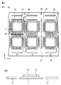
- FIG. 1A and 1B are views showing a method of manufacturing a semiconductor device according to the present invention
- FIG. 1A is a plan view showing a lead frame
- FIG. 1B is a sectional view showing a part thereof.
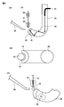
- FIG. 2 is a view showing a method for manufacturing a semiconductor device of the present invention
- (A) is a view showing a bonder (bonding device) used
- (B) is a view of a nozzle as viewed from above
- C) is a diagram showing a process of forming an initial ball.
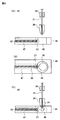
- 3A and 3B are diagrams showing a method of manufacturing a semiconductor device according to the present invention
- FIG. 3A is a diagram showing another configuration of the bonder used
- FIG. C) is a diagram showing a process of forming an initial ball.
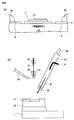
- FIG. 4A and 4B are views showing a method for manufacturing a semiconductor device according to the present invention.
- FIG. 4A is a sectional view
- FIG. 4B is a view showing a state where nozzles are aligned.
- FIG. 5 is a diagram showing a method for manufacturing a semiconductor device of the present invention.
- FIG. 6 is a cross-sectional view showing a method for manufacturing a semiconductor device of the present invention.
- 7A and 7B are views showing a method for manufacturing a semiconductor device according to the present invention, in which FIG. 7A is a plan view and FIG. 7B is a cross-sectional view.
- 8A and 8B are views showing a semiconductor device manufactured by the method for manufacturing a semiconductor device of the present invention, FIG. 8A is a perspective view, and FIG.
- FIGS. 9A and 9B are cross-sectional views.
- a lead frame 12 having a predetermined shape is prepared.
- a frame mainly made of copper is generally used.
- a frame mainly made of Fe-Ni may be used, or a frame made of another metal material may be used.
- the surface of the lead frame 12 may be covered with a plating film in which nickel, palladium and gold are laminated in this order by electrolytic plating.
- a plurality of mounting portions 13 indicated by alternate long and short dash lines are formed on the lead frame 12 made of these materials.
- one collective block may be formed by collecting the four mounting portions 13 together.
- a collective block may be configured from several tens or several hundreds of mounting parts 13 arranged in a matrix.
- resin molding is integrally performed for each assembly block in a later step.
- the mounting portion 13 includes an island 7, suspension leads 14 that support four corners of the island 7, a plurality of leads 4 that are located near the four sides of the island 7, and a tie bar 15 that supports the plurality of leads 4. Composed.
- the suspension leads 14 extend from the four corners of the island 7 and are connected to the support regions 16 where the tie bars 15 intersect.
- the support region 16 is integrated with the lead frame 12, and the island 7 is supported by the lead frame 12.
- the lead frame 12 in the region surrounding the assembly block is provided with a slit 21 that penetrates the lead frame 12 in a groove shape.
- the slit 21 has a function of suppressing the lead frame 12 from being bent by thermal stress when the lead frame 12 is heated by wire bonding or the like.
- the hole 22 is formed through the end of the lead frame 12 in a circular shape and is used for positioning the lead frame 12 in each step.
- the semiconductor element 10 is fixed to the upper surface of the island 7 of each mounting portion.
- an adhesive 9 made of a conductive adhesive such as solder or conductive paste or an insulating adhesive such as epoxy resin is used.
- an LSI having a large number of pads (electrodes) arranged on the upper surface is employed.
- the pads provided on the upper surface of the semiconductor element and the upper surface of the lead are connected using a thin metal wire (wire bonding).
- Gold, aluminum, copper, or the like can be used as the material for the fine metal wire used.
- the copper wire is, for example, a metal thin wire containing 99.9 to 99.99 wt% of copper.
- a copper wire having a lower purity than this may be adopted as the thin metal wire.
- a copper wire has an advantage that the non-resistance is small and the current capacity can be increased.
- a metal fine wire is divided roughly into a thick wire with a diameter of 33 micrometers or more and a thin wire with a diameter less than 33 micrometers, this process is applicable to both.
- the wire bonding in this step includes a step of forming an initial ball at the tip of the fine metal wire, a step of connecting the initial ball to the pad of the semiconductor element, and a step of connecting the other end of the fine metal wire to the upper surface of the inner lead. Including. When wire bonding is performed, the fine metal wire is exposed to a high temperature of 200 ° C. or higher.
- FIG. 2A is a view showing the bonder 20 (bonding apparatus) used in this process
- FIG. 2B is a view of the nozzle 24 as viewed from above
- FIG. 2C is the initial ball formed. It is a figure which shows the state to do.
- the bonder 20 used in this step includes a capillary 30, a wire clamper 32, a torch 33, and a nozzle 24 (second supply means). These parts included in the bonder 20 are fixed to a bonding arm, for example, and move together during bonding.
- the capillary 30 is a part that moves the fine metal wire 31 and gives bonding energy to the fine metal wire 31, and has a central hole through which the fine metal wire 31 is inserted.
- the wire clamper 32 is disposed above the capillary 30 and has a role of sandwiching the fine metal wire 31.
- the end portion of the torch 33 is arranged near the lower end of the capillary 30 and is discharged from the tip end of the torch 33 toward the end portion of the fine metal wire when the initial ball is formed.
- the nozzle 24 is a supply unit that blows gas toward the tip of the capillary 30 where the initial ball is formed (second supply unit).
- a mixed gas of an inert gas such as nitrogen and a reducing gas such as hydrogen is employed as the gas blown through the nozzle 24 .
- the inert gas prevents oxidation of copper, which is the material of the fine metal wires 31, and the reducing gas removes oxides existing on the surface of the fine metal wires 31 by a reducing action.
- an inert gas or a reducing gas may be employed.
- the nozzle 24 is formed by bending a lower end portion of a metal tube made of stainless steel having an inner diameter of about several millimeters at a predetermined angle.
- the tip 18 of the nozzle 24 faces the lower end of the capillary 30.
- the other end of the nozzle 24 communicates with a pump that pumps the gas.
- An optical fiber 25 (second irradiating means) that irradiates a light beam 26 is disposed inside the nozzle 24 in order to perform relative alignment between the capillary 30 and the nozzle 24.
- the vicinity of the lower end of the nozzle 24 has a curved shape.
- the light beam irradiated from the optical fiber 25 is reflected from the inner wall of the curved nozzle 24 and then externally passes from the tip 18. To be released.
- the inner wall of the nozzle 24 made of metal such as stainless steel is a surface close to a mirror surface made of metal, the light beam 26 irradiated from the optical fiber 25 is well reflected.
- the direction of the light beam emitted from the tip portion 18 of the nozzle 24 is the same as the direction of the gas emitted from the tip portion 18.
- the material of the nozzle 24 may be ceramic or metal. That is, the material is not particularly limited as long as the inner wall of the nozzle 24 is glossy enough to reflect light rays.
- the color of the light beam 26 is not particularly limited as long as it can be visually confirmed by an operator, but is preferably a color different from the illumination color inside the apparatus in which the bonder is arranged.
- the color of the light beam 26 emitted from the tip 18 of the nozzle 24 is preferably green.
- the optical fiber 25 is built in the nozzle 24, but the part where the optical fiber 25 is provided may be another part.
- the tip of the optical fiber 25 may be arranged inside the vicinity of the tip of the nozzle 24.
- the tip of the optical fiber 25 may be fixed to the outer surface near the tip of the nozzle 24. As described above, the capillary 30 is exchanged every several hundred thousand times of wire bonding.
- the positions of the nozzle 24 and the capillary 30 are adjusted so that the light beam 26 irradiated from the optical fiber 25 is irradiated to the tip of the capillary 30. Therefore, since the worker can work with reference to the light beam 26 that can be easily visually confirmed, there is an advantage that the position adjustment of both can be performed easily and reliably. Furthermore, there is an advantage that the time required for the adjustment work can be shortened as compared with the conventional example which is different from the abundant experience of the workers.
- the position of only the nozzle 24 may be adjusted, or the positions of both the nozzle 24 and the capillary 30 may be adjusted.
- the adjustment includes adjustment of the three-dimensional position of the nozzle 24 and adjustment of the direction of the tip 18 of the nozzle 24.
- the notch part 19 is formed by cutting off the front-end
- a part of the capillary 30 is disposed in the notch 19. By doing so, the tip end portion 18 of the nozzle 24 can be disposed close to the capillary 30, and when the capillary 30 moves up and down during wire bonding, it is prevented from colliding with the nozzle 24. Referring to FIG.
- the initial ball 34 is formed using the bonder 20 having the above-described configuration, first, the end of the thin metal wire 31 is led out from the lower end of the capillary 30. Next, the initial ball 34 is formed by discharging from the tip of the torch 33 toward the lower end of the fine metal wire 31.
- the fine metal wire 31 having a diameter of 45 ⁇ m is used, for example, a current of 125 mA is required when the initial ball 34 is formed.
- the initial ball 34 is formed while the gas 27 is blown toward the end of the thin metal wire 31 from the nozzle 24 whose position has been adjusted as described above. Therefore, the initial ball 34 is formed in an atmosphere of gas 27.
- FIG. 3A is a view showing the bonder 20 used in this step
- FIG. 3B is a view of the formation portion 45 used for initial ball formation from above
- FIG. 3C is the initial ball. It is sectional drawing which shows the process of forming.
- description of items common to the bonder 20 shown in FIG. 2 is omitted.
- 3A is composed of a wire clamper 32, a capillary 30, and a forming part 45 in which a torch 33 is built.
- a forming portion 45 in which the torch 33 is built is used instead of the nozzle 24 and the torch 33 provided in the bonder 20 shown in FIG. 2, a forming portion 45 in which the torch 33 is built is used.
- the formation part 45 consists of inorganic materials, such as a ceramic, and the external shape is exhibiting the rectangular parallelepiped shape elongated in the horizontal direction on the paper surface.
- Inside the formation portion 45 there are formed a conduction hole 47 provided through the inside in the longitudinal direction and a through hole 46 provided through the formation portion 45 in a cylindrical shape in the thickness direction. Further, the conduction hole 47 and the through hole 46 communicate with each other.
- a torch 33 is disposed inside the conduction hole 47, and the tip of the torch 33 is exposed inside the through hole 46. Further, since the thickness of the torch 33 is shorter than the inner diameter of the conduction hole 47, there is a gap between the torch 33 and the conduction hole 47, and the gas 27 is supplied to the through hole 46 via this gap. .
- the diameter of the through hole 46 is set larger than the diameter of the capillary 30. Further, when viewed from above, the capillary 30 is disposed inside the through hole 46. Therefore, when wire bonding is performed, the capillary 30 can move up and down via the through hole 46 of the forming portion 45. With reference to FIG.
- the capillary 30 is lowered, and the lower end of the fine metal wire 31 is positioned inside the through hole 46 of the forming portion 45.
- the initial ball 34 is formed by discharging from the torch 33 toward the lower end of the fine metal wire 31 led out from the capillary 30. Further, this step is performed while supplying the gas 27 to the through hole 46 through the conduction hole 47. Accordingly, oxidation of the metal material constituting the fine metal wire 31 is prevented, and the initial ball 34 having an ideal shape close to a spherical shape is formed.
- the bonder 20 shown in FIG. 3 is adopted as the mechanism for forming the initial ball, since the gas is not sprayed by the nozzle, the alignment by the optical fiber 25 shown in FIG. 2 (A) is unnecessary. It becomes.
- the lead frame 12 is placed on the upper surface of the placement table 43. Since the mounting table 43 is heated to about 250 to 260 ° C. by the heating mechanism, the lead frame 12 and the semiconductor element 10 mounted on the upper surface thereof are also heated to the same extent. Further, the upper surface of the lead frame 12 is pressed and fixed by a clamper 44, and the lead 4, the island 7, and the semiconductor element 10 of each mounting portion are exposed upward from the clamper 44.
- the metal fine wires are exposed to a high temperature atmosphere for a long time, and the risk of oxidation increases.
- wire bonding is performed while supplying gas, so that the risk of oxidation is reduced.
- the nozzle 39 which blows the gas 42 to the location where a metal fine wire is connected is aligned.
- a copper wire that is easily oxidized is employed as the metal thin wire 31. Therefore, in order to prevent oxidation, it is necessary to perform wire bonding in an inert gas atmosphere.
- the initial ball 34 is bonded to the pad 17 of the semiconductor element 10 fixed to the upper surface of the island 7.
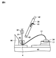
- the gas 42 is supplied from the nozzle 39 (first supply means) toward the pad 17 of the semiconductor element 10.
- the gas 42 used here also contains an inert gas and a reducing gas.
- the alignment of the nozzle 39 is performed using the optical fiber 41 (first irradiation means) built in the nozzle 39. Specifically, the light beam 40 is irradiated from the optical fiber 41 along the direction in which the gas 42 is ejected from the nozzle 39.
- the adjustment of the nozzle 39 includes adjustment of the three-dimensional position of the nozzle 39 and adjustment of the direction of the tip of the nozzle 39.
- the color of the light beam 40 used here is preferably a color (for example, green) different from the illumination color in the apparatus in which the bonder is used, as described above. This alignment is performed when, for example, the position of the pad 17 of the semiconductor element 10 that is a connection location is changed.
- the embodied bonder 20 may include the nozzle 39 illustrated in FIG. 4 and the nozzle 24 illustrated in FIG.
- both the nozzle 24 shown in FIG. 2 and the nozzle 39 shown in FIG. 4 have built-in optical fibers for position adjustment, but even if only one of the nozzles is provided with an optical fiber. good.
- an initial ball 34 provided at one end of the fine metal wire 31 is connected to the pad 17 of the semiconductor element 10.
- the capillary 30 descends toward the pad 17 of the semiconductor element 10 and presses the initial ball 34 against the upper surface of the pad 17.
- the initial ball 34 formed at the tip of the capillary 30 is connected to the pad 17 by a thermocompression bonding technique using ultrasonic vibration.
- the wire clamper is in an open state. Further, in this step, the above bonding is performed while the gas 42 is blown from the nozzle 39 toward the pad 17. Therefore, even if the initial ball 34 is connected in a high temperature atmosphere, the initial ball 34 is not oxidized. Therefore, since no oxide is present at the interface between the initial ball 34 and the pad 17, it is possible to prevent a connection failure from occurring due to the oxide under use conditions.
- the capillary 30 moves to the upper surface of the lead 4 while drawing a fixed loop.
- the capillary 30 is lowered to the upper surface of the lead 4 and presses the metal thin wire 31 against the upper surface of the lead 4.
- the fine metal wires 31 are connected to the leads 4 by a thermocompression bonding technique using ultrasonic vibration.
- the capillary 30 is raised, and the fine metal wire 31 is cut.
- bonding is performed while blowing the gas 42 from the nozzle 39 to the upper surface of the lead 4 to which the fine metal wire 31 is connected. Accordingly, no oxide is present in the boundary portion between the fine metal wire 11 and the upper surface of the lead 4, and the connection strength between the two becomes strong.
- the position of the nozzle 39 may be adjusted so that the light beam irradiated from the optical fiber 41 is irradiated to a predetermined portion of the lead 4. Thereafter, the wire bonding operation described above is repeated for all the pads 17 and the leads 4 of the semiconductor element 10.
- resin molding is performed for each aggregate block on the lead frame 12 to form a common resin package 35.
- a resin mold sheet see FIG. 7B
- the lead frame 12 is placed in a resin-sealed mold.
- a common resin package 35 is formed for each assembly block.
- FIG. 8A is a perspective view showing the semiconductor device 1
- FIG. 8B is a perspective view showing a state in which the semiconductor device 1 is turned upside down
- FIG. 8A is a perspective view showing the semiconductor device 1
- FIG. 8B is a perspective view showing a state in which the semiconductor device 1 is turned upside down
- FIG. 8A is a perspective view showing the semiconductor device 1
- FIG. 8B is a perspective view showing a state in which the semiconductor device 1 is turned upside down
- FIG. 8A is a perspective view showing a state in which the semiconductor device 1 is turned upside down
- the semiconductor device 1 is composed of, for example, a MAP type resin package 2.
- the leads 4 are exposed from the side surface 3 of the resin package 2 in order to divide into individual pieces by dicing.
- the exposed side surface of the lead 4 forms the same surface as the side surface 3 of the resin package 2.
- an island 7 is exposed on the back surface 6 of the resin package 2, and the island 7 forms substantially the same surface as the back surface 6 of the resin package 2.
- a semiconductor element 10 is fixed on the island 7 by an adhesive 9 such as Ag paste or solder.
- the pad of the semiconductor element 10 and the lead 4 are electrically connected by a thin metal wire 11.
- a thin metal wire 11 for example, a copper wire made of copper having a diameter of 33 to 50 ⁇ m and 99.9 to 99.99 wt% is used.
- the fine metal wires 11 are ball-bonded on the pads of the semiconductor element 10 and stitch-bonded on the leads 4.
- the island 7 and the leads 4 surrounding the island 7 are made of, for example, a frame whose main material is copper having a thickness of about 100 to 250 ⁇ m.
- a lead frame on which a discrete transistor in which an island is connected to a collector electrode is mounted may be employed.
- a lead frame or a printed circuit board that realizes SIP by combining a semiconductor element such as an LSI and a passive element such as a chip resistor may be used.
Landscapes
- Wire Bonding (AREA)
Abstract
供給されるガスの経路を容易に確認することを可能とするボンディング装置およびそれを用いた半導体装置の製造方法を提供する。本発明のボンディング装置は、ワイヤクランパー32とキャピラリ30と、トーチ33とノズル39とを備え、ノズル39から不活性なガス42を接続箇所に吹き付けつつ、ワイヤボンディングを行っている。そして、ノズル39の内部には、ガス42が吹き付けられる方向に沿って光線40を照射する光ファイバー41が内蔵されている。従って、光ファイバー41から照射される光線40が、接続箇所であるパッド17に照射されるように、ノズル39の位置調整を行うことで、ガス42をパッド17に対して適切に吹きつけることが可能と成る。
Description
本発明は、金属細線により半導体素子の電気的接続を行うボンディング装置およびそれを用いた半導体装置の製造方法に関する。
従来の半導体装置の製造方法の一実施例として、下記の製造方法が知られている。
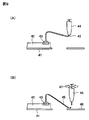
先ず、図9(A)に示す如く、リードフレームのダイパッド41上に半導体素子42を固着した後、リードフレームをボンディング装置に設置する。半導体素子42のパッド43を約200℃に加熱し、キャピラリ44がパッド43上へと移動する。そして、超音波振動併用の熱圧着技術により、キャピラリ44の先端に形成された金属ボールをパッド43へと接続する。一般にこれをボールボンディングと言う。
次に、図9(B)に示す如く、キャピラリ44がインナーリード46の先端部上方へ移動し、インナーリード46に対し金属細線45を所望の荷重にて押し付ける。このとき、インナーリード46を約200℃に加熱し、インナーリード46に対し超音波振動併用の熱圧着技術により金属細線45を接続する。その後、ワイヤクランパー47を閉じた状態にてキャピラリ44が上昇し、金属細線45をインナーリード46の接続箇所にて破断する。一般にこれをステッチボンディングと言う。
そして、上記したワイヤーボンディング作業を繰り返すことで、半導体素子42の全てのパッドとインナーリードとを金属細線45にて電気的に接続する(例えば、特許文献1参照。)。
ここで、半導体素子42の接続に用いられる金属細線45が酸化した状態でワイヤボンディングされると接続不良が発生する恐れがある。特に、金属細線45のイニシャルボールと半導体素子42のパッド43との界面に酸化物が介在すると、使用状況下にて両者が界面から分離してしまい接続不良となる恐れがある。このような金属細線45が酸化してしまう現象は、金属細線45の材料として酸化しやすい銅が採用された場合に顕著に発生する。
ワイヤボンディング時に、Cuから成る金属細線が酸化することを防止する技術として、例えば下記特許文献2に記載された技術がある。この公報の図3を参照すると、還元ガスや不活性ガスの雰囲気下で、金属細線の先端部にボールを形成することにより、ボールを形成する際の酸化を防止する事項が開示されている。
上記した特許文献2に記載されているように、Cuの金属細線にボールを形成する際に、この作業を不活性ガスの雰囲気下にて行うことで、ボール表面の酸化が防止される。
しかしながら、一般的にキャピラリは数十万回程度のワイヤボンディング毎に新しいものに取り替えられ、この交換に伴いキャピラリの位置が若干ずれる。そして、キャピラリの位置がずれると、不活性ガスを供給する手段とキャピラリとの相対的な位置もずれてしまう。このように成ると、ボール形成時に、キャピラリの下端から導出される金属細線の端部に、不活性ガスが適切に供給されず、ボールが酸化する恐れがある。
また、酸化しやすい銅から成る金属細線のワイヤボンディングを行う際には、金属細線が接続される接続箇所(半導体素子のパッドやリードの上面)に、別の供給手段から不活性ガスを供給する必要がある。そして、この供給を精密に行うためには、この供給手段と接続箇所との位置合わせを行い、供給される不活性ガスが接続箇所に適切に供給されているか否かを確認する必要がある。しかしながら、この供給手段の調整には、作業員の豊富な経験と長い作業時間が必要とされる問題があった。この理由は、供給される不活性ガスが透明であり、このガスが吹き付けられている状況を目視で確認できないからである。
本発明は、上記した問題点を鑑みてなされ、本発明の目的は、供給されるガスの経路を容易に確認し、このガスを供給する供給手段の位置調整を正確に行うことを可能とするボンディング装置およびそれを用いた半導体装置の製造方法を提供することにある。
本発明のボンディング装置は、金属細線が挿通されるキャピラリと、前記金属細線に対して放電することで前記金属細線の端部にイニシャルボールを形成するトーチと、前記金属細線が接続される接続箇所に対してガスを吹き付ける第1供給手段と、前記イニシャルボールが形成される際に、前記キャピラリの下端に対してガスを吹き付ける第2供給手段と、前記第1供給手段または前記第2供給手段から前記ガスが吹き付けられる方向に沿って光線を照射する第1照射手段と、を備えることを特徴とする。
本発明の半導体装置の製造方法は、キャピラリと、前記キャピラリの近傍に配置されたトーチと、前記キャピラリが金属細線を接続する接続箇所に対してガスを吹き付ける第1供給手段と、前記キャピラリの先端部付近に対してガスを吹き付ける第2供給手段とを備えたボンディング装置を用意する工程と、前記金属細線の一端を前記キャピラリから突出させ、前記第2供給手段から前記ガスを前記金属細線の一端に吹きつけつつ、前記金属細線の前記端部に対して前記トーチから放電することによりイニシャルボールを形成する工程と、半導体素子のパッドに対して第1供給手段から前記ガスを吹き付けつつ、前記パッドに前記イニシャルボールを接続する工程と、前記金属細線の他端を、前記半導体素子と接続されるリードの主面に接続する工程と、を備え、前記第1供給手段または前記第2供給手段から前記ガスが吹き付けられる方向に沿って光線を照射し、前記第1供給手段または前記第2供給手段の位置を調整することを特徴とする。
本発明の半導体装置の製造方法は、キャピラリと、前記キャピラリの近傍に配置されたトーチと、前記キャピラリが金属細線を接続する接続箇所に対してガスを吹き付ける第1供給手段と、前記キャピラリの先端部付近に対してガスを吹き付ける第2供給手段とを備えたボンディング装置を用意する工程と、前記金属細線の一端を前記キャピラリから突出させ、前記第2供給手段から前記ガスを前記金属細線の一端に吹きつけつつ、前記金属細線の前記端部に対して前記トーチから放電することによりイニシャルボールを形成する工程と、半導体素子のパッドに対して第1供給手段から前記ガスを吹き付けつつ、前記パッドに前記イニシャルボールを接続する工程と、前記金属細線の他端を、前記半導体素子と接続されるリードの主面に接続する工程と、を備え、前記第1供給手段または前記第2供給手段から前記ガスが吹き付けられる方向に沿って光線を照射し、前記第1供給手段または前記第2供給手段の位置を調整することを特徴とする。
本発明によれば、金属細線が接続される箇所に対して第1供給手段からガスを供給し、この供給手段がガスを吹きつける箇所に対して第1照射手段により光を照射している。このことにより、第1照射手段が照射する光を視覚的に認識することで、ガスが供給されている箇所を確認することができる。従って、照射される光が接続箇所に照射される様に第1供給手段の位置および向きを調整することより、第1供給手段から接続箇所に向かってガスが適切に供給される。このことから、調整作業が容易に成ると共に、半導体素子のパッド等の接続箇所に金属細線が接続される際の酸化が防止される。
更に本発明によれば、イニシャルボールが形成されるキャピラリの先端に対して第2供給手段によりガスを供給し、第2供給手段がガスを吹き付ける方向に沿って第2照射手段から光線を照射している。このようにすることで、キャピラリの交換によりその位置がずれても、第2照射手段から照射される光線を視覚的に確認しつつ両者の位置関係を調整することができる。具体的には、ボールが形成されるキャピラリの先端部に、第2照射手段から照射される光が照射されるように、第2供給手段の位置及び向きを調整することで、第2供給手段から供給されるガスが適切な箇所に供給される。従って、金属細線の先端にイニシャルボールを形成する際の酸化が防止され、球形に近い理想的な形状のイニシャルボールが金属細線の先端に形成される。
更に本発明によれば、イニシャルボールが形成されるキャピラリの先端に対して第2供給手段によりガスを供給し、第2供給手段がガスを吹き付ける方向に沿って第2照射手段から光線を照射している。このようにすることで、キャピラリの交換によりその位置がずれても、第2照射手段から照射される光線を視覚的に確認しつつ両者の位置関係を調整することができる。具体的には、ボールが形成されるキャピラリの先端部に、第2照射手段から照射される光が照射されるように、第2供給手段の位置及び向きを調整することで、第2供給手段から供給されるガスが適切な箇所に供給される。従って、金属細線の先端にイニシャルボールを形成する際の酸化が防止され、球形に近い理想的な形状のイニシャルボールが金属細線の先端に形成される。
図1は本発明の半導体装置の製造方法を示す図であり、(A)はリードフレームを示す平面図であり、(B)はその一部を示す断面図である。
図2は本発明の半導体装置の製造方法を示す図であり、(A)は使用されるボンダー(ボンディング装置)を示す図であり、(B)はノズルを上方から見た図であり、(C)はイニシャルボールを形成する工程を示す図である。
図3は本発明の半導体装置の製造方法を示す図であり、(A)は使用されるボンダーの他の構成を示す図であり、(B)は形成部を上方からみた図であり、(C)はイニシャルボールを形成する工程を示す図である。
図4は本発明の半導体装置の製造方法を示す図であり、(A)は断面図であり、(B)はノズルの位置合わせを行う状態を示す図である。
図5は本発明の半導体装置の製造方法を示す図である。
図6は本発明の半導体装置の製造方法を示す断面図である。
図7は本発明の半導体装置の製造方法を示す図であり、(A)は平面図であり、(B)は断面図である。
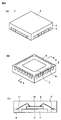
図8は本発明の半導体装置の製造方法により製造される半導体装置を示す図であり、(A)は斜視図であり、(B)は半導体装置の表裏を逆転させた状態を示す斜視図であり,(C)は断面図である。
図9は従来の実施の形態における半導体装置の製造方法を示す図であり、(A)および(B)は断面図である。
本形態の半導体装置の製造方法およびボンディング装置を以下に説明する。
図1(A)を参照して、先ず、所定形状のリードフレーム12を用意する。リードフレーム12としては、一般には銅を主材料とするフレームが用いられるが、Fe−Niを主材料とするフレームの場合でも良く、他の金属材料から成る場合でも良い。また、リードフレーム12の表面はニッケル、パラジュームおよび金をこの順序で電解メッキにより積層させたメッキ膜により被覆されても良い。そして、これらの材料から成るリードフレーム12には、一点鎖線で示す搭載部13が複数形成される。尚、図1を参照して、この搭載部13が4つ集まることで1つの集合ブロックが形成されても良い。また、マトリックス状に配置された数十または数百個の搭載部13から集合ブロックが構成されても良い。この場合は、後の工程にて集合ブロック毎に一体に樹脂モールドされる。
搭載部13は、アイランド7と、アイランド7の4隅を支持する吊りリード14と、アイランド7の4側辺の近傍に位置する複数のリード4と、複数のリード4を支持するタイバー15とから構成される。そして、吊りリード14はアイランド7の4つのコーナー部から延在し、タイバー15の交差する支持領域16と連結する。支持領域16はリードフレーム12と一体となり、アイランド7がリードフレーム12に支持される。
更にまた、集合ブロックを囲む領域のリードフレーム12には、リードフレーム12を溝状に貫通したスリット21が設けられている。このスリット21は、ワイヤボンディング等にてリードフレーム12が加熱された際に、リードフレーム12が熱応力で撓むことを抑制する機能を有する。孔22は、リードフレーム12の端部を円形に貫通して形成されており、各工程にてリードフレーム12の位置決めを行うために用いられる。
図1(B)を参照して、次に、各搭載部のアイランド7の上面には、半導体素子10が固着されている。この固着には、半田、導電性ペースト等の導電性接着材またはエポキシ樹脂等の絶縁性接着材から成る接着材9が用いられる。半導体素子10としては、上面に多数個のパッド(電極)が配置されたLSIが採用される。
図2から図6を参照して、次に、半導体素子の上面に設けられたパッドとリードの上面とを、金属細線を用いて接続する(ワイヤボンディング)。使用される金属細線の材料としては、金、アルミニウム、銅等が採用可能であるが、本工程では金属細線の材料として銅から成る銅線を用いた場合を説明する。ここで、銅線とは、例えば99.9~99.99wt%で銅を含む金属細線である。更には、これよりも純度が低い銅線が金属細線として採用されても良い。
金属細線の材料として安価な銅を用いることで材料コストが低減される利点がある。更に、金線と比較すると、銅線は非抵抗が小さく電流容量が大きく取れる利点もある。また、金属細線は、直径が33μm以上の太線と、直径が33μm未満の細線に大別されるが、本工程は両者に適用可能である。
本工程のワイヤボンディングは、金属細線の先端にイニシャルボールを形成する工程と、このイニシャルボールを半導体素子のパッドに接続する工程と、金属細線の他端をインナーリードの上面に接続する工程とを含む。ワイヤボンディングを行う際には、金属細線は200℃以上の高温にさらされるので、銅から成る金属細線の酸化を防止するために本工程では金属細線に対してガスを供給している。更に本形態では、ガスを供給する供給手段の位置合わせのために光線を使用している。この事項を以下に詳述する。
図2を参照して、金属細線の先端部にイニシャルボールを形成する工程を説明する。図2(A)は本工程にて用いられるボンダー20(ボンディング装置)を示す図であり、図2(B)はノズル24を上方からみた図であり、図2(C)はイニシャルボールを形成する状態を示す図である。
図2(A)を参照して、本工程で用いられるボンダー20は、キャピラリ30と、ワイヤクランパー32と、トーチ33と、ノズル24(第2供給手段)とを備えている。ボンダー20に含まれるこれらの部位は、例えばボンディングアームに固定され、ボンディング時には一体的に移動する。
キャピラリ30は金属細線31を移動すると共に、金属細線31に対してボンディングエネルギーを与える部位であり、金属細線31が挿通されるための中心孔を備えている。
ワイヤクランパー32は、キャピラリ30の上方に配置されており金属細線31を狭持する役割を有する。
トーチ33の端部は、キャピラリ30の下端付近に配置され、イニシャルボールを形成する際には、トーチ33の先端から金属細線の端部に向かって放電される。
ノズル24は、イニシャルボールが形成されるキャピラリ30の先端部に対して、ガスを吹き付ける供給手段である(第2供給手段)。ここで、ノズル24を経由して吹き付けられるガスとしては、窒素等の不活性ガスと水素等の還元ガスとの混合ガスが採用される。不活性ガスは金属細線31の材料である銅の酸化を防止し、還元ガスは金属細線31の表面に存在する酸化物を還元作用により除去する。また、ガスとしては、不活性ガスまたは還元ガスの何れかが採用されても良い。
ノズル24は、内径が数ミリ程度のステンレス等から成る金属管の下端部を所定角度に湾曲して形成されている。ノズル24の先端部18は、キャピラリ30の下端を向いている。ノズル24の他の端部は、上記したガスを圧送するポンプと連通している。
ノズル24の内部には、キャピラリ30とノズル24との相対的な位置合わせを行うために、光線26を照射する光ファイバー25(第2照射手段)が配置されている。この図からも明らかなように、ノズル24の下端部付近は湾曲形状を呈しているが、光ファイバー25から照射された光線は、湾曲するノズル24の内壁で反射された後に、先端部18から外部に放出される。ステンレス等の金属から成るノズル24の内壁は、金属から成る鏡面に近い状態の面であるので、光ファイバー25から照射された光線26を良好に反射する。また、ノズル24の先端部18から外部の放射される光線の向きは、先端部18から放出されるガスの向きと同じである。ここで、ノズル24の材料はセラミックや金属でも良い。即ち、ノズル24の内壁が光線を反射させる程度の光沢を備えていれば、その材料は特に限定されない。
光線26の色は、作業員が視覚的に確認可能な色であれば特に制限はないが、ボンダーが配置される装置内部の照明色とは異なる色が好適である。例えば、ボンダーが配置される装置内部の照明色が赤系の色である場合は、ノズル24の先端部18から放射される光線26の色としては緑色が好ましい。このようにすることで、ノズル24から出射される光線26を容易に目視で確認することができる。
またここで、光ファイバー25はノズル24に内蔵されているが、光ファイバー25が備えられる箇所は他の部位でも良い。例えば、ノズル24の先端部付近の内部に光ファイバー25の先端が配置されてもよいし。更には、ノズル24の先端付近の外面に光ファイバー25の先端が固定されても良い。
上記した様に、数十万回程度のワイヤボンディング毎にキャピラリ30は交換されるが、その際には、据え付けられた新たなキャピラリ30とノズル24との位置合わせを行う必要がある。即ち、イニシャルボールが形成される際に、ノズル24からガスがキャピラリ30の先端に吹き付けられるように調整する必要がある。本形態では、光ファイバー25から照射される光線26が、キャピラリ30の先端に照射される様に、ノズル24とキャピラリ30との位置を調整している。従って、作業員は容易に視覚的に確認できる光線26を基準として作業が行えるので、両者の位置調整が容易且つ確実に行える利点がある。更には、作業員の豊富な経験に異存していた従来例と比較すると、この調整作業にかかる時間が短縮化される利点もある。
また、この際には、ノズル24のみの位置調整が行われてもよいし、ノズル24およびキャピラリ30の両方の位置調整が行われても良い。ここで、調整とは、ノズル24の3次元位置の調整や、ノズル24の先端部18の向きの調整を含む。
図2(B)を参照して、ノズル24の先端部18を部分的に円形に切り取ることにより、切りかき部19が形成されている。そして、上方から見た場合、キャピラリ30の一部は切りかき部19に配置されている。このようにすることで、ノズル24の先端部18をキャピラリ30に接近して配置できると共に、キャピラリ30がワイヤボンディング時に昇降した際に、ノズル24に衝突することが防止される。
図2(C)を参照して、上記した構成のボンダー20を用いてイニシャルボール34を形成する際には、先ず、キャピラリ30の下端から金属細線31の端部を下方に導出させる。次に、トーチ33の先端部から金属細線31の下端に向かって放電することにより、イニシャルボール34が形成される。ここで、径が45μmの金属細線31を用いた場合、イニシャルボール34の形成時には、例えば、125mAの電流が必要となる。
また、本工程では、上記のように位置調整が施されたノズル24から、金属細線31の端部に向かってガス27を吹き付けつつ、上記したイニシャルボール34を形成している。従って、イニシャルボール34の形成はガス27の雰囲気下にて行われる。上記したように、ガス27は不活性ガスおよび還元ガスを含むので、本工程による金属細線31の酸化は防止され、イニシャルボール34の球面形状が安定して形成される。
図3を参照して、上記したイニシャルボール34を形成する他の方法を説明する。図3(A)は本工程で用いるボンダー20を示す図であり、図3(B)はイニシャルボール形成に用いられる形成部45を上方から見た図であり、図3(C)はイニシャルボールを形成する工程を示す断面図である。ここで、図2に示したボンダー20と共通する事項については説明を割愛する。
図3(A)に示すボンダー20は、ワイヤクランパー32と、キャピラリ30と、トーチ33が内蔵された形成部45とから構成されている。ここでは、図2に示したボンダー20が備えるノズル24およびトーチ33に替えて、トーチ33が内蔵された形成部45が用いられている。
形成部45は、セラミック等の無機材料から成り、外形形状は紙面上にて横方向に細長い直方体形状を呈している。形成部45の内部には、長手方向に内部を貫通して設けた導通孔47と、形成部45を厚み方向に円柱状に貫通して設けた貫通孔46が形成されている。また、導通孔47と貫通孔46とは連通している。
導通孔47の内部にはトーチ33が配置されており、トーチ33の先端部は貫通孔46の内部に露出している。また、トーチ33の太さは導通孔47の内径よりも短いので、トーチ33と導通孔47との間には間隙が存在し、この間隙を経由してガス27が貫通孔46に供給される。
図3(B)を参照して、貫通孔46の直径はキャピラリ30の直径よりも大きく設定されている。更に、上方から見た場合、キャピラリ30は貫通孔46の内部に配置される。従って、ワイヤボンディングを行う際には、形成部45の貫通孔46を経由して、キャピラリ30が上下に移動することが可能と成る。
図3(C)を参照して、上記した構成のボンダーでイニシャルボール34を形成する方法を説明する。先ず、金属細線31の下端をキャピラリ30から下方に導出させた後に、キャピラリ30を降下させ、金属細線31の下端を、形成部45の貫通孔46の内部に位置させる。次に、キャピラリ30から導出する金属細線31の下端に向かって、トーチ33から放電することにより、イニシャルボール34を形成する。また、本工程は、導通孔47を経由してガス27を貫通孔46に供給しつつ行う。従って、金属細線31を構成する金属材料の酸化を防止して、球形状に近い理想的な形状のイニシャルボール34が形成される。
ここで、イニシャルボールを形成する機構として図3に示したボンダー20が採用された場合は、ノズルによるガスの吹き付けが行われないので、図2(A)に示した光ファイバー25による位置合わせが不要となる。
図4(A)を参照して、ワイヤボンディングの工程では、リードフレーム12は、載置台43の上面に載置されている。載置台43は加熱機構により250~260℃程度に加熱されているので、その上面に載置されるリードフレーム12および半導体素子10も同程度に加熱される。また、リードフレーム12の上面はクランパー44により押圧固定されており、各搭載部のリード4、アイランド7および半導体素子10は、このクランパー44から上方に露出している。
ここで、多数個の搭載部が一活してワイヤボンディングされる場合、金属細線が長時間にわたり高温の雰囲気下に晒され酸化の危険性が高まる。しかしながら、本願発明を適用することにより、ガスを供給しつつワイヤボンディングを行うので酸化の危険性が低減される。
図4(B)を参照して、次に、金属細線が接続される箇所にガス42を吹き付けるノズル39の位置合わせを行う。
本形態では、金属細線31として酸化しやすい銅線を採用しているので、酸化を防ぐ為には、ワイヤボンディングを不活性ガスの雰囲気下にて行う必要がある。ここでは、イニシャルボール34は、アイランド7の上面に固着された半導体素子10のパッド17にボンディングされる。従って、半導体素子10のパッド17に向かって、ノズル39(第1供給手段)からガス42が供給される。また、ここで使用されるガス42も、不活性ガスおよび還元ガスを含む。ワイヤボンディング時のイニシャルボール34の酸化を防止するためには、イニシャルボール34がボンディングされる箇所に向かって、正確にガス42を噴射させる必要がある。
ここでは、図2に示した場合と同様に、ノズル39に内蔵された光ファイバー41(第1照射手段)を用いて、ノズル39の位置合わせを行っている。具体的には、ノズル39からガス42が噴射される方向に沿って、光ファイバー41から光線40が照射される。従って、半導体素子10の上面に配置されたパッド17の上面に光線40が照射されるように、ノズル39の位置を調整することで、ガス42が適切にパッド17に噴射されるように成る。ここで、ノズル39の調整は、ノズル39の3次元位置の調整やノズル39の先端部の向きの調整を含む。
また、ここで使用される光線40の色は、先に述べたように、ボンダーが使用される装置内の照明色とは異なる色(例えば緑色)が好ましい。また、この位置合わせは、例えば接続箇所である半導体素子10のパッド17の位置が変更された際に行われる。
ここで、具現化されたボンダー20は、図4に示すノズル39と図2に示すノズル24とを備えて良いし、図4に示すノズル39と図3に示す形成部45とを備えても良い。
更にまた、上記説明では、図2に示すノズル24および図4に示すノズル39の両方に、位置調整のための光ファイバーが内蔵されているが、どちらか一方のノズルのみに光ファイバーが設けられても良い。
図5を参照して、次に、金属細線31の一端に設けられたイニシャルボール34を、半導体素子10のパッド17に接続する。具体的には、キャピラリ30が半導体素子10のパッド17に向かって下降し、イニシャルボール34をパッド17の上面に押し付ける。そして、超音波振動併用の熱圧着技術により、キャピラリ30の先端に形成されたイニシャルボール34がパッド17と接続する。尚、この作業時には、ワイヤークランパーは開放された状態である。
更に本工程では、ノズル39からガス42をパッド17に向かって吹き付けつつ、上記したボンディングを行う。従って、高温の雰囲気下にてイニシャルボール34の接続を行っても、イニシャルボール34が酸化することはない。このことから、イニシャルボール34とパッド17との界面に酸化物が介在しないので、この酸化物に起因した使用状況下での接続不良の発生が防止される。
図6を参照して、次に、ワイヤクランパー32が開放された状態にて、一定のループを描きながらキャピラリ30がリード4の上面に移動する。その後、ワイヤクランパー32にて金属細線31を挟持した後、キャピラリ30がリード4の上面に下降し、金属細線31をリード4の上面に押し付ける。そして、超音波振動併用の熱圧着技術により金属細線31がリード4と接続する。その後、キャピラリ30が上昇し、金属細線31を切断する。本工程に於いても、金属細線31が接続されるリード4の上面に対して、ノズル39からガス42を吹き付けつつボンディングを行う。従って、金属細線11とリード4の上面の境界部分にも酸化物は介在せず、両者の接続強度が強固となる。また、この工程での酸化を確実に抑制するために、光ファイバー41から照射される光線がリード4の所定箇所に照射されるように、ノズル39の位置を調整しても良い。
その後、半導体素子10の全てのパッド17とリード4に対して、上述したワイヤーボンディング作業を繰り返す。
次に、図7(A)に示す如く、リードフレーム12上の集合ブロック毎に樹脂モールドし、共通の樹脂パッケージ35を形成する。例えば、リードフレーム12の裏面側に樹脂モールド用のシート(図7(B)参照)を貼り合せた後、リードフレーム12を樹脂封止金型内に配置する。そして、樹脂封止金型内に絶縁性樹脂を充填することで、集合ブロック毎に共通の樹脂パッケージ35を形成する。上述したように、共通の樹脂パッケージ35内には、4つの搭載部13が含まれる。
最後に、図7(B)に示す如く、リードフレーム12から搭載部13毎に共通の樹脂パッケージ35を切断して、個々の樹脂パッケージ2に個片化する。切断にはダイシング装置のダイシングブレード37を用い、ダイシングライン38に沿って共通の樹脂パッケージ35とリードフレーム12とを同時にダイシングする。このとき、シート36は、その一部のみが切断されることで、個片化された個々の樹脂パッケージ2はシート36上に支持される。
図8を参照して、上記工程により製造される半導体装置の構成を説明する。図8(A)は半導体装置1を示す斜視図であり、図8(B)は半導体装置1を表裏逆にした状態を示す斜視図であり、図8(C)はその断面図である。
図8(A)に示す如く、半導体装置1は、例えば、MAP方式の樹脂パッケージ2から成る。上記したように、集合ブロックを一括封止後、ダイシングにより個片化するため、樹脂パッケージ2の側面3からリード4が露出する。そして、露出するリード4の側面は、樹脂パッケージ2の側面3と同一面を形成する。
図8(B)に示す如く、樹脂パッケージ2の裏面6にはアイランド7が露出し、このアイランド7は、樹脂パッケージ2の裏面6とほぼ同一面を形成する。
図8(C)を参照して、アイランド7上には、例えば、Agペースト、半田等の接着材9により半導体素子10が固着される。半導体素子10のパッドとリード4とは金属細線11により電気的に接続される。金属細線11は、例えば、径が33~50μm、99.9~99.99wt%の銅から成る銅線が使用される。そして、金属細線11は、半導体素子10のパッド上にボールボンディングされ、リード4上にステッチボンディングされる。
アイランド7およびその周囲を囲むリード4は、例えば、厚さが約100~250μmの銅を主材料とするフレームから成る。
以上が、本形態の半導体装置の製造方法により製造される半導体装置1の構成である。
ここで、リードフレームとしてIC用のリードフレームを採用して上記説明を行ったが、銅から成る金属細線が使用されるのであればリードフレームの形状は特に限定されない。例えば、アイランドがコレクタ電極に接続されるディスクリートのトランジスタが実装されるリードフレームが採用されても良い。更には、LSI等の半導体素子とチップ抵抗等の受動素子が組み合わせてSIPが実現されるリードフレームやプリント基板が使用されても良い。
1 半導体装置
2 パッケージ
3 側面
4 リード
6 裏面
7 アイランド
9 接着材
10 半導体素子
11 金属細線
12 リードフレーム
13 搭載部
14 吊りリード
15 タイバー
16 支持領域
17 パッド
18 先端部
19 切りかき部
20 ボンダー
21 スリット
22 孔
24 ノズル
25 光ファイバー
26 光線
27 ガス
30 キャピラリ
31 金属細線
32 ワイヤクランパー
33 トーチ
34 イニシャルボール
35 パッケージ
36 シート
37 ダイシングブレード
38 ダイシングライン
39 ノズル
40 光線
41 光ファイバー
42 ガス
43 載置台
44 クランパー
45 形成部
46 貫通孔
47 導通孔
Claims (9)
- 金属細線が挿通されるキャピラリと、
前記金属細線に対して放電することで前記金属細線の端部にイニシャルボールを形成するトーチと、
前記金属細線が接続される接続箇所に対してガスを吹き付ける第1供給手段と、
前記イニシャルボールが形成される際に、前記キャピラリの下端に対してガスを吹き付ける第2供給手段と、
前記第1供給手段または前記第2供給手段から前記ガスが吹き付けられる方向に沿って光線を照射する第1照射手段と、
を備えることを特徴とするボンディング装置。 - 前記第1照射手段は、前記第1供給手段に内蔵された光ファイバーであることを特徴とする請求項1に記載のボンディング装置。
- 前記第1照射手段から照射される前記光線が、半導体素子のパッドに照射されるように、前記第1供給手段の位置が調整されることを特徴とする請求項1または請求項2に記載のボンディング装置。
- 前記第2供給手段から前記ガスが吹き付けられる方向に沿って光線を照射する第2照射手段を更に備え、
前記第2照射手段から照射される光線が前記キャピラリの下端に照射されるように、前記第2供給手段と前記キャピラリとの相対的な位置が調整されることを特徴とする請求項3に記載のボンディング装置。 - 前記第2供給手段は、先端部分が湾曲する金属管から成るノズルであり、前記第2照射手段から照射された光線は、前記ノズルの内壁で反射された後に前記先端部分から外部に放射されることを特徴とする請求項4に記載のボンディング装置。
- 前記金属細線は、銅線であることを特徴とする請求項1から請求項5の何れかに記載のボンディング装置。
- 前記光線の色は、ワイヤボンディングが行われる装置内部の照明色とは異なる色であることを特徴とする請求項1から請求項6の何れかに記載のボンディング装置。
- キャピラリと、前記キャピラリの近傍に配置されたトーチと、前記キャピラリが金属細線を接続する接続箇所に対してガスを吹き付ける第1供給手段と、前記キャピラリの先端部付近に対してガスを吹き付ける第2供給手段とを備えたボンディング装置を用意する工程と、
前記金属細線の一端を前記キャピラリから突出させ、前記第2供給手段から前記ガスを前記金属細線の一端に吹きつけつつ、前記金属細線の前記端部に対して前記トーチから放電することによりイニシャルボールを形成する工程と、
半導体素子のパッドに対して第1供給手段から前記ガスを吹き付けつつ、前記パッドに前記イニシャルボールを接続する工程と、
前記金属細線の他端を、前記半導体素子と接続されるリードの主面に接続する工程と、を備え、
前記第1供給手段または前記第2供給手段から前記ガスが吹き付けられる方向に沿って光線を照射し、前記第1供給手段または前記第2供給手段の位置を調整することを特徴とする半導体装置の製造方法。 - 前記第2供給手段から前記ガスが吹き付けられる方向に沿って光線を照射し、前記キャピラリの下端に前記光線が照射されるように、前記キャピラリと前記第2供給手段との位置を調整することを特徴とする請求項8に記載の半導体装置の製造方法。
Applications Claiming Priority (2)
| Application Number | Priority Date | Filing Date | Title |
|---|---|---|---|
| JP2010-70099 | 2010-03-25 | ||
| JP2010070099 | 2010-03-25 |
Publications (1)
| Publication Number | Publication Date |
|---|---|
| WO2011118247A1 true WO2011118247A1 (ja) | 2011-09-29 |
Family
ID=44672825
Family Applications (1)
| Application Number | Title | Priority Date | Filing Date |
|---|---|---|---|
| PCT/JP2011/051148 Ceased WO2011118247A1 (ja) | 2010-03-25 | 2011-01-17 | ボンディング装置およびそれを用いた半導体装置の製造方法 |
Country Status (1)
| Country | Link |
|---|---|
| WO (1) | WO2011118247A1 (ja) |
Citations (5)
| Publication number | Priority date | Publication date | Assignee | Title |
|---|---|---|---|---|
| JPS55138246A (en) * | 1979-04-13 | 1980-10-28 | Toshiba Corp | Manufacture of semicondoctor device |
| JPH01256135A (ja) * | 1988-04-06 | 1989-10-12 | Hitachi Ltd | ワイヤボンディング装置 |
| JPH08162490A (ja) * | 1994-12-02 | 1996-06-21 | Hitachi Ltd | ボンディング装置 |
| JP2008034811A (ja) * | 2006-07-03 | 2008-02-14 | Shinkawa Ltd | ワイヤボンディング装置におけるボール形成装置及びボンディング装置 |
| JP2010023190A (ja) * | 2008-07-22 | 2010-02-04 | Shigeo Ueda | 照明付きノズル |
-
2011
- 2011-01-17 WO PCT/JP2011/051148 patent/WO2011118247A1/ja not_active Ceased
Patent Citations (5)
| Publication number | Priority date | Publication date | Assignee | Title |
|---|---|---|---|---|
| JPS55138246A (en) * | 1979-04-13 | 1980-10-28 | Toshiba Corp | Manufacture of semicondoctor device |
| JPH01256135A (ja) * | 1988-04-06 | 1989-10-12 | Hitachi Ltd | ワイヤボンディング装置 |
| JPH08162490A (ja) * | 1994-12-02 | 1996-06-21 | Hitachi Ltd | ボンディング装置 |
| JP2008034811A (ja) * | 2006-07-03 | 2008-02-14 | Shinkawa Ltd | ワイヤボンディング装置におけるボール形成装置及びボンディング装置 |
| JP2010023190A (ja) * | 2008-07-22 | 2010-02-04 | Shigeo Ueda | 照明付きノズル |
Similar Documents
| Publication | Publication Date | Title |
|---|---|---|
| CN104465414B (zh) | 半导体器件的制造方法 | |
| CN101378051B (zh) | 半导体器件及其制造方法 | |
| JP7827729B2 (ja) | 構成可能なリード付きパッケージ | |
| US8847410B2 (en) | Semiconductor chip with bonding wire and method for making the same | |
| JP2010080914A (ja) | 樹脂封止型半導体装置とその製造方法、リードフレーム | |
| JP4711549B2 (ja) | 半導体装置の製造方法 | |
| TWI531016B (zh) | Semiconductor device and manufacturing method thereof | |
| JP2003007759A (ja) | 認識装置、ボンディング装置および回路装置の製造方法 | |
| US11145617B2 (en) | Semiconductor structure | |
| US20080286959A1 (en) | Downhill Wire Bonding for QFN L - Lead | |
| JP2014216416A (ja) | 半導体発光装置およびその製造方法 | |
| JP2006156437A (ja) | リードフレーム及び半導体装置 | |
| CN102856281A (zh) | 半导体封装件及其制造方法 | |
| CN100424864C (zh) | 提高封装可靠性的导线架及其封装结构 | |
| JP2014187308A (ja) | 半導体装置の製造方法 | |
| JP5411529B2 (ja) | 半導体装置の製造方法 | |
| KR100660821B1 (ko) | 와이어본딩 방법 | |
| JP5411553B2 (ja) | 半導体装置の製造方法 | |
| JP2011238663A (ja) | 半導体装置の製造方法、ワイヤーボンディング装置 | |
| JP2007012642A (ja) | ワイヤボンディング方法 | |
| CN201994269U (zh) | 封装打线工艺的压板构造 | |
| JP4717129B2 (ja) | 半導体装置の製造方法 | |
| JP2011233667A (ja) | 半導体装置の製造方法、ワイヤーボンディング装置及び半導体装置 | |
| JP2007035863A (ja) | 半導体装置 | |
| JP2011204861A (ja) | 半導体装置の製造方法 |
Legal Events
| Date | Code | Title | Description |
|---|---|---|---|
| 121 | Ep: the epo has been informed by wipo that ep was designated in this application |
Ref document number: 11759056 Country of ref document: EP Kind code of ref document: A1 |
|
| NENP | Non-entry into the national phase |
Ref country code: DE |
|
| 122 | Ep: pct application non-entry in european phase |
Ref document number: 11759056 Country of ref document: EP Kind code of ref document: A1 |
|
| NENP | Non-entry into the national phase |
Ref country code: JP |