WO2011114968A1 - 金型製造方法およびその方法により形成された金型 - Google Patents
金型製造方法およびその方法により形成された金型 Download PDFInfo
- Publication number
- WO2011114968A1 WO2011114968A1 PCT/JP2011/055539 JP2011055539W WO2011114968A1 WO 2011114968 A1 WO2011114968 A1 WO 2011114968A1 JP 2011055539 W JP2011055539 W JP 2011055539W WO 2011114968 A1 WO2011114968 A1 WO 2011114968A1
- Authority
- WO
- WIPO (PCT)
- Prior art keywords
- film
- layer
- group
- mold
- metal
- Prior art date
- Legal status (The legal status is an assumption and is not a legal conclusion. Google has not performed a legal analysis and makes no representation as to the accuracy of the status listed.)
- Ceased
Links
Images




Classifications
-
- G—PHYSICS
- G03—PHOTOGRAPHY; CINEMATOGRAPHY; ANALOGOUS TECHNIQUES USING WAVES OTHER THAN OPTICAL WAVES; ELECTROGRAPHY; HOLOGRAPHY
- G03F—PHOTOMECHANICAL PRODUCTION OF TEXTURED OR PATTERNED SURFACES, e.g. FOR PRINTING, FOR PROCESSING OF SEMICONDUCTOR DEVICES; MATERIALS THEREFOR; ORIGINALS THEREFOR; APPARATUS SPECIALLY ADAPTED THEREFOR
- G03F7/00—Photomechanical, e.g. photolithographic, production of textured or patterned surfaces, e.g. printing surfaces; Materials therefor, e.g. comprising photoresists; Apparatus specially adapted therefor
- G03F7/0002—Lithographic processes using patterning methods other than those involving the exposure to radiation, e.g. by stamping
-
- B—PERFORMING OPERATIONS; TRANSPORTING
- B82—NANOTECHNOLOGY
- B82Y—SPECIFIC USES OR APPLICATIONS OF NANOSTRUCTURES; MEASUREMENT OR ANALYSIS OF NANOSTRUCTURES; MANUFACTURE OR TREATMENT OF NANOSTRUCTURES
- B82Y10/00—Nanotechnology for information processing, storage or transmission, e.g. quantum computing or single electron logic
-
- B—PERFORMING OPERATIONS; TRANSPORTING
- B82—NANOTECHNOLOGY
- B82Y—SPECIFIC USES OR APPLICATIONS OF NANOSTRUCTURES; MEASUREMENT OR ANALYSIS OF NANOSTRUCTURES; MANUFACTURE OR TREATMENT OF NANOSTRUCTURES
- B82Y40/00—Manufacture or treatment of nanostructures
-
- Y—GENERAL TAGGING OF NEW TECHNOLOGICAL DEVELOPMENTS; GENERAL TAGGING OF CROSS-SECTIONAL TECHNOLOGIES SPANNING OVER SEVERAL SECTIONS OF THE IPC; TECHNICAL SUBJECTS COVERED BY FORMER USPC CROSS-REFERENCE ART COLLECTIONS [XRACs] AND DIGESTS
- Y10—TECHNICAL SUBJECTS COVERED BY FORMER USPC
- Y10T—TECHNICAL SUBJECTS COVERED BY FORMER US CLASSIFICATION
- Y10T428/00—Stock material or miscellaneous articles
- Y10T428/24—Structurally defined web or sheet [e.g., overall dimension, etc.]
- Y10T428/24479—Structurally defined web or sheet [e.g., overall dimension, etc.] including variation in thickness
- Y10T428/24612—Composite web or sheet
Definitions
- the present invention relates to a mold manufacturing method and a mold formed by the method, and is particularly suitable for application to a mold having a fine structure.
- Fig. 12 shows a conventional mold manufacturing method.
- a resist is applied to a glass substrate or Si substrate 100, and a pattern 101 is formed on the resist using ultraviolet rays, electron beams, X-rays, or the like.
- a conductive layer 102 is formed thereon by sputtering (for example, Patent Document 1).
- Ni plating is performed on the conductive layer 102 to form a metal film 103, and the metal film 103 is released to obtain a mold 104.
- a submicron level fine structure can be performed without any trouble such as embedding plating in a hole.
- an object of the present invention is to provide a mold manufacturing method capable of easily manufacturing a mold having a nano-sized fine structure and a mold formed by the method.
- the invention according to claim 1 of the present invention provides a mold manufacturing method in which a metal film is formed on an inorganic thin film having a fine structure, and the metal film is separated from the inorganic thin film to form a mold.
- an energization layer forming step of forming an energization layer on the self-assembled film and a step of forming the metal film on the energization layer is a silane coupling agent having a functional group including one or more of an amino group, a mercapto group, a thiol group, a disulfide group, a cyano group, a halogen group, and a sulf
- the conducting layer forming step includes the steps of forming a metal ion layer on the self-assembled film, immersing the metal ion layer in a reducing solution, and reducing the metal ion layer, Forming a thin film plating layer on the metal ion layer.
- the metal ion layer comprises the self-assembled film formed on the inorganic thin film in a solution containing at least one of Au, Pd, Ag, Pt, Bi, and Pb. It is formed by dipping.
- a mold in which a metal film is formed on an inorganic thin film having a fine structure, and the metal film is separated from the inorganic thin film.
- Forming a self-assembled film containing a silane coupling agent having a functional group containing at least one of a group, a mercapto group, a thiol group, a disulfide group, a cyano group, a halogen group, and a sulfonic acid group A conductive layer having a metal ion layer is formed thereon, and a metal film is formed on the conductive layer by electrolytic plating.
- the invention according to claim 5 of the present invention is characterized in that the current-carrying layer has a thin film plating layer formed on the metal ion layer by electroless Ni plating.
- the invention according to claim 6 of the present invention is characterized in that the metal film is formed by electrolytic Ni plating.
- the invention according to claim 7 of the present invention is characterized in that an adhesion force between the metal film and the inorganic thin film is 10 MPa to 50 MPa.
- a mold having a nano-sized fine structure can be easily manufactured.
- FIG. 8A is an electron micrograph showing the results according to Example 1 of the present invention
- FIG. 8A is a surface of a Si oxide film after separating a conductive layer
- FIG. 8B is a mold surface obtained by separating from the surface of a Si oxide film.
- FIG. It is a figure which shows schematic structure of the measuring apparatus used for the measurement of the adhesive force in Example 2 which concerns on this invention.
- FIG. 12A and 12B are cross-sectional views showing a conventional mold manufacturing method step by step, FIG. 12A shows a state in which a pattern is formed on a substrate, FIG. 12B shows a state in which a conductive layer is formed on the pattern, and FIG. FIG. 12D is a diagram showing a state in which the Ni plating layer is separated by the mold release process.
- the mold manufacturing method according to the present invention comprises a self-assembled monolayer (SAM) on an inorganic thin film 1 having a fine nano-sized pattern. 2), the current-carrying layer 3 can be uniformly formed on the pattern. As a result, the metal film 4 is formed by more reliably embedding the plating in the pattern.
- the mold 5 having the structure can be easily manufactured.
- the current-carrying layer 3 serves as an electrode when performing electroplating to form the metal film 4.
- the mold manufacturing method first, a nano-sized pattern is formed on the inorganic thin film 1.
- the pattern has illustrated the thing of the two-dimensional structure which consists of unevenness
- the method for forming the pattern is not particularly limited, and a known technique can be used.
- the inorganic thin film 1 is made of a Si oxide film formed on the surface of the Si substrate 6.
- a resist is applied to the inorganic thin film 1, a mask is used to expose a predetermined pattern with ultraviolet rays, electron beams, X-rays, and the like, and the pattern is formed using dry etching.
- a self-assembled film 2 is grown on the inorganic thin film 1.
- the self-assembled film 2 is composed of a monomolecular film made of a silane coupling agent having a functional group including one or more of an amino group, a mercapto group, a thiol group, a disulfide group, a cyano group, a halogen group, and a sulfonic acid group. ing.
- the self-assembled film 2 is formed by using the first solution containing the silane coupling agent and chemically adsorbing on the surface of the inorganic thin film 1 by liquid phase growth or vapor phase growth.
- the first solution containing the silane coupling agent and chemically adsorbing on the surface of the inorganic thin film 1 by liquid phase growth or vapor phase growth In the case of liquid phase growth, it can be formed by immersing the Si substrate 6 on which the self-assembled film 1 is formed in the first solution.
- the vapor can be formed by applying the vapor obtained by evaporating the first solution to the self-assembled film 1 formed on the Si substrate 6.
- the first solution for example, a solution obtained by heating a toluene solution containing 10% of 3-aminopropyltrimethoxysilane (APTMS) shown in Chemical Formula 1 as a silane coupling agent to 60 degrees can be applied.
- the self-assembled film 2 has another terminal functional group on the opposite side to the functional group chemisorbed on the surface of the inorganic thin film 1.
- the molecular arrangement interval is determined by van der Waals force of the alkyl group.
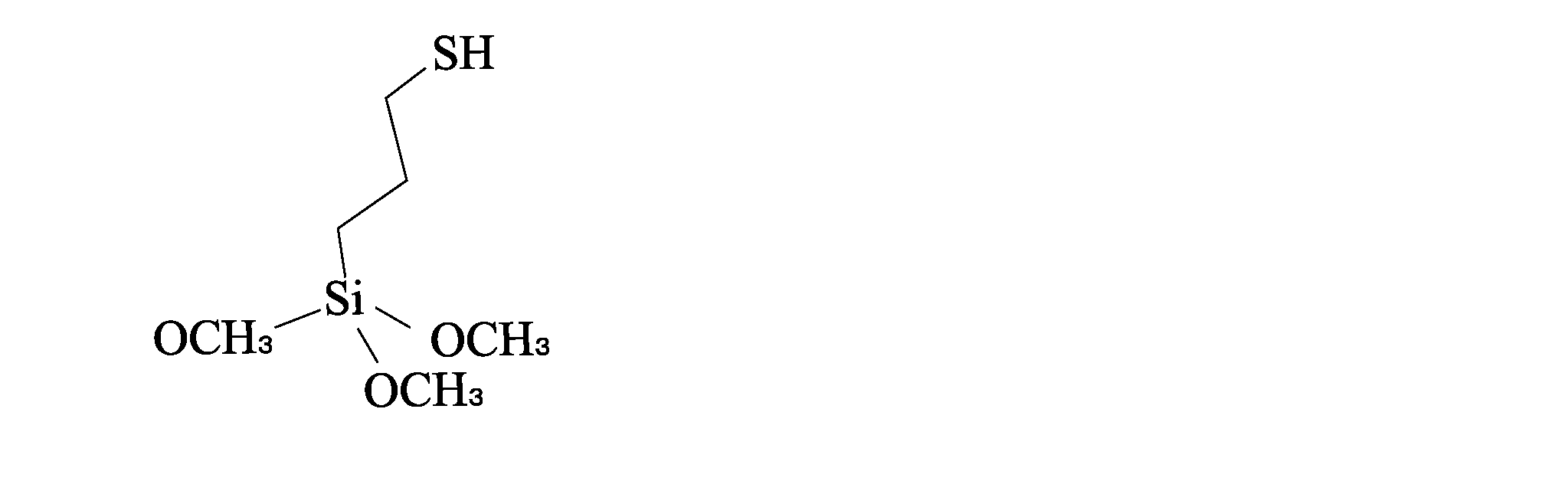
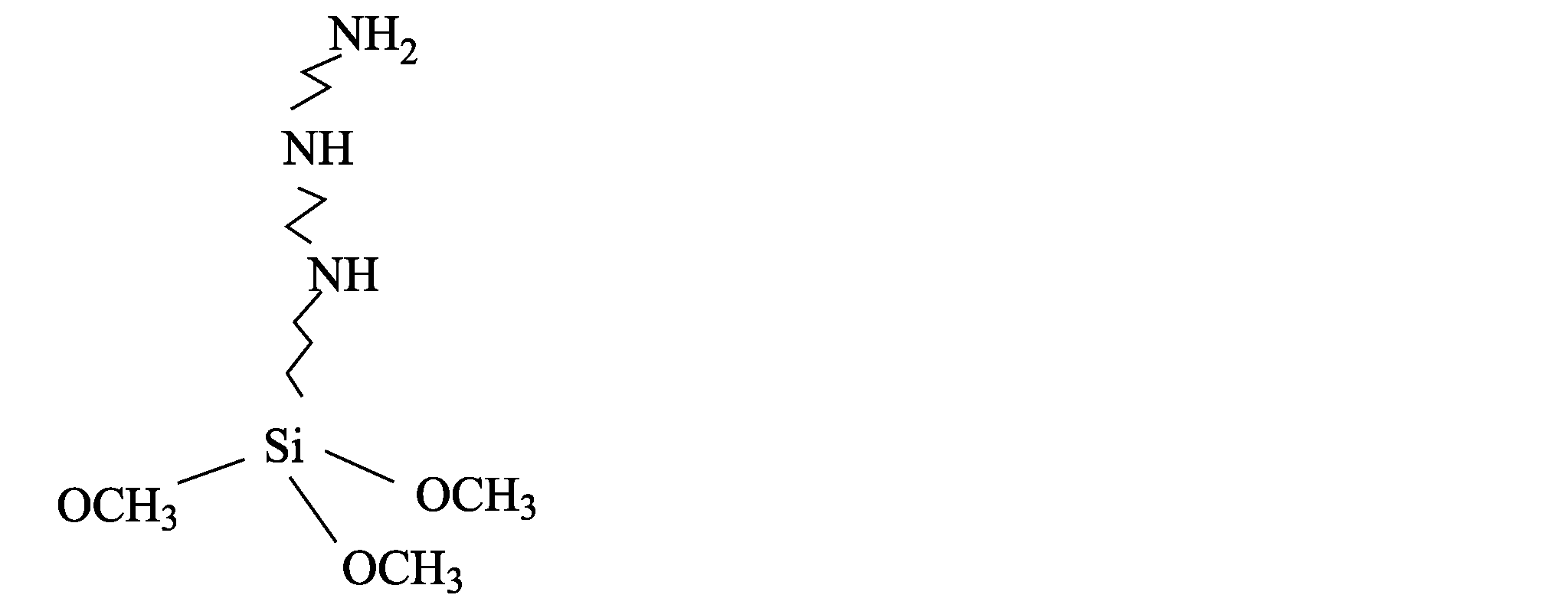
- silane coupling agent examples include mercaptopropyltrimethoxysilane (MPTMS) represented by Chemical Formula 2, 3- [2- (2-aminoethylamino) ethylamino] propyltrimethoxysilane (TAS) represented by Chemical Formula 3 and the like. Can be applied.
- MPTMS mercaptopropyltrimethoxysilane
- TAS propyltrimethoxysilane
- the conductive layer 3 is formed on the self-assembled film 2.
- the energization layer 3 includes a metal ion layer formed on the self-assembled film 2 and a thin film plating layer formed on the metal ion layer.
- the metal ion layer is formed by immersing the self-assembled film 2 formed on the inorganic thin film 1 in a second solution containing one or more of Au, Pd, Ag, Pt, Bi, and Pb.
- the metal ions contained in the second solution are chemically adsorbed on the terminal functional group of the self-assembled film 2.
- the solvent used for the second solution include dilute hydrochloric acid, dilute nitric acid, dilute sulfuric acid, and the like.
- the self-assembled film 2 is formed by chemisorption as shown in FIG. 5 on the Si oxide film surface as the inorganic thin film 1.
- a metal ion layer is formed on the surface of the self-assembled film 2 by adsorbing metal ions (Au + in this figure).
- the thin film plating layer is formed by electroless plating using a weakly acidic plating bath.
- Various metals can be applied to the thin film plating layer, and for example, it can be formed of Ni, Co, Pt, Sn, Au, Cu, or the like.
- the surface of the metal ion layer is immersed in a reducing solution to reduce the oxidized metal ion layer, thereby forming the thin film plating layer reliably. More preferred above.
- the metal film 4 is formed on the conductive layer 3 by electrolytic plating.
- This metal film 4 can be formed by a known method. For example, electrolytic Ni plating can be applied.
- the metal mold 5 including the conductive layer 3 and the metal film 4 can be obtained by separating the conductive layer 3 and the inorganic thin film 1.
- the adhesive force between the inorganic thin film 1 and the conductive layer 3 is preferably 10 MPa or more and 50 MPa or less. If the adhesion force is less than 10 MPa, peeling occurs partially during the manufacturing process, for example, during the formation of the energization layer, resulting in a failure. On the other hand, if the adhesive force exceeds 50 MPa, it is difficult to release the mold, and the metal film may be damaged in some cases and become defective.
- the self-assembled film 2 composed of a silane coupling agent is formed on the inorganic thin film 1 having a nano-sized pattern, so that the conductive layer 3 is uniformly formed on the pattern. Can be formed. Accordingly, since the plating can be more reliably embedded in the nano-sized pattern by electrolytic plating using the current-carrying layer 3 as an electrode, a mold having a nano-sized fine structure can be easily manufactured.
- the energization layer 3 includes the metal ion layer and the thin film plating layer, it is possible to more reliably form an electrode required when the metal film 4 is formed by electrolytic plating.
- the chemical adsorption of the metal ion layer on the self-assembled film 2 stops the growth of the metal ion layer because no further adsorption reaction occurs when metal ions are adsorbed to all of the terminal functional groups of the self-assembled film 2. . Therefore, it is usually preferable to form a thin film plating on the metal ion layer in order to ensure the thickness required for the electrode for electrolytic plating, but it is possible to grow the metal ion layer to the thickness required for the electrode for electrolytic plating. If possible, the current-carrying layer 3 can be composed of only a metal ion layer by omitting the thin film plating layer.
- Example 1 a nano-sized pattern was formed on a Si oxide film as an inorganic thin film formed on a Si substrate.
- a 1-inch wafer was used as the Si substrate. Further, the size of the formed pattern is 200 nm in diameter.
- a self-assembled film was formed on the pattern by liquid phase growth.
- a self-assembled film was formed by immersing a toluene solution containing 1 wt.% Of a silane coupling agent as a first solution in a solution heated to 60 ° C. for 10 minutes.
- a silane coupling agent 3- [2- (2-aminoethylamino) ethylamino] propyltrimethoxysilane (TAS) was used.
- a metal ion layer and a thin film plating layer were formed in this order as an energization layer.
- the metal ion layer was formed by immersing a Si substrate on which a self-assembled film was formed in a solution containing Pd as the second solution for 1 minute. Dilute hydrochloric acid was used as the solvent. Note that the Pd concentration in the second solution is 1 mM.
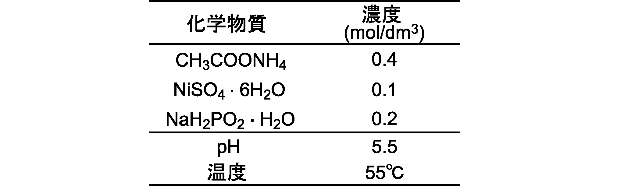
- the thin film plating layer was formed by electroless Ni plating by immersing a Si substrate on which a metal ion layer was formed in an electroless Ni plating bath shown in Table 1 for 5 minutes.
- the Si substrate on which the conductive layer thus formed was formed was immersed in an electrolytic Ni plating bath, and the conductive layer was energized to form a metal film having a thickness of about 300 ⁇ m.
- die was obtained by isolate
- a metal film could be formed in the same manner using 3-aminopropyltrimethoxysilane (APTMS) or mercaptopropyltrimethoxysilane (MPTMS) as the silane coupling agent.
- APIMS 3-aminopropyltrimethoxysilane
- MPTMS mercaptopropyltrimethoxysilane
- a mold having a nano-sized fine structure can be manufactured by forming a current-carrying layer on a self-assembled film composed of a silane coupling agent. It was.
- Example 2 Next, the adhesion between the inorganic thin film and the conductive layer was confirmed.
- a self-assembled film is formed on a Si substrate using 3- [2- (2-aminoethylamino) ethylamino] propyltrimethoxysilane (TAS) as a silane coupling agent, and Pd is formed on the self-assembled film. Then, an electroless sample was formed on the metal ion layer.
- a Si substrate subjected to Sn—Pd treatment was formed.
- the measurement apparatus 10 shown in FIG. 9 was used for the measurement of the adhesion force.
- the measuring apparatus 10 includes an electronic digital balance 11, a displacement meter 12, a piezoelectric actuator 13, a microscope 14, and an electronic calculator 15.
- the sample pan 16 is provided on the electronic digital balance 11.
- the sample pan 16 is configured to hold the sample S in a state where the sample S is inclined at a predetermined angle.
- the predetermined angle is 30 degrees.
- the piezoelectric actuator 13 is provided integrally with the displacement meter 12 and is provided with an indenter 17 that makes contact with the metal film 4 formed on the sample S.
- the displacement meter 12 is configured as a non-contact type, and irradiates light to a mirror 18 provided on the sample dish 16 and detects a change in intensity of reflected light of the light, whereby the indentation depth of the indenter 17 is detected. It is comprised so that can be measured.
- the microscope 14 is provided so that the surface of the sample S installed on the sample dish 16 can be observed.
- the piezoelectric actuator 13 was moved toward the sample dish 16 and the indenter 17 was pressed against the metal film 4.
- the moving speed of the piezoelectric actuator 13 was 10 nm / s.
- the load on the metal film 4 of the indenter 17 was measured with the electronic digital balance 11. It was judged that the conductive layer was separated from the inorganic thin film at the point where the load was extremely reduced (FIG. 10), and the load was defined as the adhesion force. The results are shown in FIG.
- the adhesion force between the self-assembled film and the Si oxide film was in the range of 10 MPa to 50 MPa without depending on the thickness of the thin film plating layer.
- the adhesion force depends on the combination of the silane coupling agent and the inorganic thin film constituting the self-assembled film. .
- the comparative example (“Sn-Pd" in the figure) is a metal bond, it was confirmed that the adhesion was greater than that of this example, and that the variation in adhesion was also greater than this example. .
- a desired adhesion can be obtained by selecting a silane coupling agent. (Modification)
- the present invention is not limited to the above embodiment, and can be appropriately changed within the scope of the gist of the present invention.
- the mold manufacturing method manufactures a mold having a two-dimensional structure made of unevenness
- the present invention is not limited to this, and the self-assembled film is a pattern of a three-dimensional structure.
- a three-dimensional mold can be manufactured in the same manner.
- the present invention is not limited to this, and may be formed by vapor phase growth.
Landscapes
- Engineering & Computer Science (AREA)
- Chemical & Material Sciences (AREA)
- Nanotechnology (AREA)
- Physics & Mathematics (AREA)
- Crystallography & Structural Chemistry (AREA)
- General Physics & Mathematics (AREA)
- Manufacturing & Machinery (AREA)
- Condensed Matter Physics & Semiconductors (AREA)
- Mathematical Physics (AREA)
- Theoretical Computer Science (AREA)
- Moulds For Moulding Plastics Or The Like (AREA)
- Shaping Of Tube Ends By Bending Or Straightening (AREA)
- Exposure Of Semiconductors, Excluding Electron Or Ion Beam Exposure (AREA)
- Laminated Bodies (AREA)
- Other Surface Treatments For Metallic Materials (AREA)
Abstract
ナノサイズの微細構造を有する金型を容易に製造することができる金型製造方法およびその方法により形成された金型を提供する。 微細構造を有した無機薄膜1上にアミノ基、メルカプト基、チオール基、ジスルフィド基、シアノ基、ハロゲン基、スルフォン酸基の1つ以上を含む官能基を有するシランカップリング剤から構成された自己組織化膜2を形成するステップと、前記自己組織化膜2上に通電層3を形成する通電層形成ステップと、前記通電層3上に電解めっきにより金属膜4を形成するステップとを有することを特徴とする。
Description
本発明は、金型製造方法およびその方法により形成された金型に関し、特に微細構造を有する金型に適用して好適なものである。
従来の金型作製方法を図12に示す。ガラス基板またはSi基板100にレジストを塗布し、紫外線、電子線、X線などを用い、レジストにパターン101を形成する。この上に通電層102をスパッタリング法用い、形成する(例えば、特許文献1)。次いで、通電層102上にNiめっきを施して金属膜103を形成し、当該金属膜103を離型して金型104を得る。
上記従来の方法によれば、サブミクロンレベルの微細構造であれば、ホールへのめっきの埋め込みなど支障なく行うことができる。
さらなる高密度、高機能化への対応として、より微細なナノサイズの微細構造、3次元構造の形状とするため、微細パターンを形成することが必要とされるが、従来の方法ではホールへのめっきの埋め込みができないなどの問題が生じていた。
また、3次元構造では通電層をスパッタ法で形成した場合にはカバレッジ不足により通電層の形成が難しい状況であった。
そこで、本発明は、ナノサイズの微細構造を有する金型を容易に製造することができる金型製造方法およびその方法により形成された金型を提供することを目的とする。
本発明の請求項1に係る発明は、微細構造を有した無機薄膜上に金属膜を形成し、前記金属膜を前記無機薄膜から分離して金型を形成する金型製造方法において、前記無機薄膜上にアミノ基、メルカプト基、チオール基、ジスルフィド基、シアノ基、ハロゲン基、スルフォン酸基の1つ以上を含む官能基を有するシランカップリング剤を含有する自己組織化膜を形成するステップと、前記自己組織化膜上に通電層を形成する通電層形成ステップと前記通電層上に前記金属膜を形成するステップとを有することを特徴とする。
本発明の請求項2に係る発明は、前記通電層形成ステップは、前記自己組織化膜上に金属イオン層を形成するステップと、前記金属イオン層を還元溶液に浸漬させ還元させるステップと、前記金属イオン層上に薄膜めっき層を形成するステップとを有することを特徴とする。
本発明の請求項3に係る発明は、前記金属イオン層は、Au、Pd、Ag、Pt、Bi、Pbのいずれか1以上を含む溶液に前記無機薄膜上に形成した前記自己組織化膜を浸漬させることより形成されることを特徴とする。
本発明の請求項4に係る発明は、微細構造を有した無機薄膜上に金属膜を形成し、前記金属膜を前記無機薄膜から分離して形成される金型において、前記無機薄膜上にアミノ基、メルカプト基、チオール基、ジスルフィド基、シアノ基、ハロゲン基、スルフォン酸基の1つ以上を含む官能基を有するシランカップリング剤を含有する自己組織化膜を形成し、前記自己組織化膜上に金属イオン層を有する通電層を形成し、前記通電層上に電解めっきにより金属膜を形成したことを特徴とする。
本発明の請求項5に係る発明は、前記通電層は、前記金属イオン層上に無電解Niめっきにより形成した薄膜めっき層を有することを特徴とする。
本発明の請求項6に係る発明は、前記金属膜は、電解Niめっきにより形成されたことを特徴とする。
本発明の請求項7に係る発明は、前記金属膜と前記無機薄膜との密着力が10MPa~50MPaであることを特徴とする。
本発明によれば、ナノサイズの微細構造を有する金型を容易に製造することができる。
以下、図面を参照して本発明の実施形態について詳細に説明する。
(製造方法)
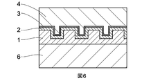
本発明に係る金型製造方法は、図1に示すように、ナノサイズの微細なパターンを有する無機薄膜1上に自己組織化単分子膜(SAM: Self-Assembled Monolayer、以下「自己組織化膜」という。)2を形成することにより、通電層3を前記パターン上に均一に形成することができ、これにより、パターンにめっきをより確実に埋め込んで金属膜4を形成し、ナノサイズの微細構造を有する金型5を容易に製造することができる。この場合、通電層3は、金属膜4を形成する電解めっきを行う際の電極となる。
(製造方法)
本発明に係る金型製造方法は、図1に示すように、ナノサイズの微細なパターンを有する無機薄膜1上に自己組織化単分子膜(SAM: Self-Assembled Monolayer、以下「自己組織化膜」という。)2を形成することにより、通電層3を前記パターン上に均一に形成することができ、これにより、パターンにめっきをより確実に埋め込んで金属膜4を形成し、ナノサイズの微細構造を有する金型5を容易に製造することができる。この場合、通電層3は、金属膜4を形成する電解めっきを行う際の電極となる。
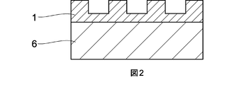
図2に示すように、金型製造方法では、まず、無機薄膜1にナノサイズのパターンを形成する。本実施形態の場合、パターンは、凹凸からなる二次元構造のものを例示している。パターンを形成する方法は、特に限定されるものではなく、公知技術を用いることができる。本実施形態の場合、無機薄膜1は、Si基板6の表面に形成したSi酸化膜からなる。この無機薄膜1にレジストを塗布して、マスクを用いて所定パターンに紫外線、電子線、X線などを露光し、ドライエッチングを用いて上記パターンを形成する。
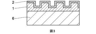
次いで、図3に示すように、金型製造方法では、無機薄膜1上に自己組織化膜2を成長させる。自己組織化膜2は、アミノ基、メルカプト基、チオール基、ジスルフィド基、シアノ基、ハロゲン基、スルフォン酸基の1つ以上を含む官能基を有するシランカップリング剤からなる単分子膜で構成されている。
自己組織化膜2は、上記シランカップリング剤を含有する第1の溶液を用い、液相成長によってあるいは気相成長によって、無機薄膜1表面に化学吸着することにより形成される。液相成長の場合は、自己組織化膜1を形成したSi基板6を前記第1の溶液に浸漬させて形成することができる。また、気相成長の場合は、前記第1の溶液を蒸発させて得た蒸気をSi基板6に形成した自己組織化膜1にあてることにより形成することができる。
第1の溶液は、例えば、シランカップリング剤として化1に示す3-アミノプロピルトリメトキシシラン(APTMS)を10%含んだトルエン溶液を60度に加温した溶液を適用することができる。自己組織化膜2は、無機薄膜1表面に化学吸着した官能基とは反対側にもう一つ末端官能基を有する。自己組織化膜2は、アルキル基のファンデルワールス力により分子の配列間隔が決定される。

また、シランカップリング剤としては、化2に示すメルカプトプロピルトリメトキシシラン(MPTMS)や、化3に示す3-[2-(2-アミノエチルアミノ)エチルアミノ]プロピルトリメトキシシラン(TAS)などを適用することができる。
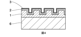
次いで、図4に示すように、金型製造方法では、自己組織化膜2上に通電層3を形成する。通電層3は、図示しないが、自己組織化膜2上に形成される金属イオン層と、当該金属イオン層上に形成される薄膜めっき層とを有する。金属イオン層は、Au、Pd、Ag、Pt、Bi、Pbの1種以上を含有する第2の溶液に無機薄膜1上に形成した自己組織化膜2を浸漬させことより形成される。この場合、第2の溶液に含有される金属イオンは、自己組織化膜2の末端官能基に化学吸着する。第2の溶液に用いられる溶媒としては、例えば、希塩酸、希硝酸、希硫酸などが挙げられる。
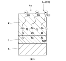
例えば、シランカップリング剤としてメルカプトプロピルトリメトキシシラン(MPTMS)を用いた場合、無機薄膜1としてのSi酸化膜表面に対し、自己組織化膜2は、図5に示すように化学吸着により形成される。また、自己組織化膜2の表面には、金属イオン(本図では、Au+)が吸着することにより金属イオン層が形成される。
上記のようにして形成された金属イオン層を核として、薄膜めっき層は弱酸性のめっき浴を用いて、無電解めっきにより形成される。薄膜めっき層は、種々の金属を適用することができるが、例えば、Ni,Co,Pt,Sn,Au,Cuなどで形成することができる。
なお、金属イオン層を形成した後、薄膜めっき層を形成する前に、金属イオン層の表面を還元溶液に浸漬し、酸化した金属イオン層を還元させることが、薄膜めっき層を確実に形成する上でより好ましい。
次いで、図6に示すように、金型製造方法では、通電層3上に金属膜4を電解めっきにより形成する。この金属膜4は、公知の方法により形成することができる。例えば、電解Niめっきを適用することができる。
最後に、図7に示すように、金型製造方法では、通電層3と無機薄膜1とを分離することにより、通電層3と金属膜4からなる金型5を得ることができる。この場合、無機薄膜1と通電層3との間の密着力が10MPa以上50MPa以下であることが好ましい。密着力が10MPa未満では製造工程中、例えば通電層を形成中に部分的に剥がれが発生し、不良となる。一方、密着力が50MPa超では離型が困難であって、場合によって金属膜が損傷し、不良となる。
(作用および効果)
本発明に係る金型製造方法では、シランカップリング剤で構成された自己組織化膜2をナノサイズのパターンを有する無機薄膜1上に形成したことにより、当該パターン上に通電層3を均一に形成することができる。したがって、前記通電層3を電極として電解めっきによりナノサイズのパターンにめっきをより確実に埋め込むことができるので、ナノサイズの微細構造を有する金型を容易に製造することができる。
本発明に係る金型製造方法では、シランカップリング剤で構成された自己組織化膜2をナノサイズのパターンを有する無機薄膜1上に形成したことにより、当該パターン上に通電層3を均一に形成することができる。したがって、前記通電層3を電極として電解めっきによりナノサイズのパターンにめっきをより確実に埋め込むことができるので、ナノサイズの微細構造を有する金型を容易に製造することができる。
また、通電層3は、金属イオン層と薄膜めっき層とを有することにより、金属膜4を電解めっきにより形成する際に必要となる電極をより確実に形成することができる。
なお、自己組織化膜2に対する金属イオン層の化学吸着は、自己組織化膜2の末端官能基の全てに金属イオンが吸着するとそれ以上吸着反応が起こらないため、金属イオン層の成長が停止する。したがって、通常、電解めっきの電極に必要な厚さを確保するため、金属イオン層上に薄膜めっきを形成することが好ましいが、金属イオン層を電解めっきの電極に必要な厚さまで成長させることができる場合、通電層3は、薄膜めっき層を省略して金属イオン層のみで構成することができる。
以下、実施例について説明する。
(実施例1)
まず、Si基板上に形成した無機薄膜としてのSi酸化膜にナノサイズのパターンを形成した。Si基板は、1インチのウェーハを用いた。また、形成したパターンのサイズは、直径200nmである。
(実施例1)
まず、Si基板上に形成した無機薄膜としてのSi酸化膜にナノサイズのパターンを形成した。Si基板は、1インチのウェーハを用いた。また、形成したパターンのサイズは、直径200nmである。
次いで、上記パターン上に自己組織化膜を液相成長により形成した。本実施例では、第1溶液としてシランカップリング剤を1wt.%含んだトルエン溶液を60℃に加温した溶液に10分間浸漬して自己組織化膜を形成した。シランカップリング剤として、3-[2-(2-アミノエチルアミノ)エチルアミノ]プロピルトリメトキシシラン(TAS)を用いた。
次いで、通電層として、金属イオン層と、薄膜めっき層とを順に形成した。金属イオン層は、第2溶液としてPdを含む溶液に自己組織化膜を形成したSi基板を1分間浸漬して形成した。溶媒には、希塩酸を用いた。なお、第2溶液におけるPd濃度は、1mMである。
薄膜めっき層は、表1に示す無電解Niめっき浴に金属イオン層を形成したSi基板を5分間浸漬して無電解Niめっきにより形成した。
このように形成した通電層を形成したSi基板を電解Niめっき浴に浸漬し、通電層に通電して厚さ300μm程度の金属膜を形成した。そして、通電層とSi酸化膜との間で分離して金型を得た。その結果を図8に示す。図8Bに示すように、本実施例に係る金型製造方法においてナノサイズの微細構造が金型に再現できることを確認できた。
また、シランカップリング剤として、3-アミノプロピルトリメトキシシラン(APTMS)、メルカプトプロピルトリメトキシシラン(MPTMS)を用いても同様に金属膜を形成できることを確認した。
以上より、本発明に係る金型製造方法では、シランカップリング剤で構成される自己組織化膜上に通電層を形成することにより、ナノサイズの微細構造を有する金型を製造できることが確認できた。
(実施例2)
次に無機薄膜と通電層との間の密着力について確認した。シランカップリング剤として3-[2-(2-アミノエチルアミノ)エチルアミノ]プロピルトリメトキシシラン(TAS)を用いて自己組織化膜をSi基板上に形成し、当該自己組織化膜上にPdの金属イオン層を形成し、さらに当該金属イオン層上に無電解試料を形成した。比較例としてSn-Pd処理を施したSi基板を形成した。
次に無機薄膜と通電層との間の密着力について確認した。シランカップリング剤として3-[2-(2-アミノエチルアミノ)エチルアミノ]プロピルトリメトキシシラン(TAS)を用いて自己組織化膜をSi基板上に形成し、当該自己組織化膜上にPdの金属イオン層を形成し、さらに当該金属イオン層上に無電解試料を形成した。比較例としてSn-Pd処理を施したSi基板を形成した。
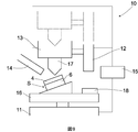
密着力の測定には、図9に示す測定装置10を用いた。測定装置10は、電子デジタル天秤11、変位計12、圧電アクチュエータ13、顕微鏡14、および電子計算機15を備える。
電子デジタル天秤11には、試料皿16が設けられている。当該試料皿16は、試料Sを所定角度に傾けた状態で保持し得るように構成されている。なお、本実施例において所定角度は、30度とした。
圧電アクチュエータ13は、変位計12と一体的に設けられており、試料Sに形成された金属膜4に当接させる圧子17が設けられている。変位計12は、非接触型で構成されており、試料皿16に設けられた鏡18に光を照射し、当該光の反射光の強度の変化を検出することにより、圧子17の押し込み深さを計測し得るように構成されている。顕微鏡14は、試料皿16に設置された試料Sの表面を観察し得るように設けられている。
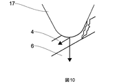
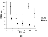
このように構成された測定装置10において、圧電アクチュエータ13を試料皿16へ向かって移動させ、圧子17を金属膜4に押し当てた。この場合の圧電アクチュエータ13の移動速度は10nm/sとした。圧子17の金属膜4に対する荷重を電子デジタル天秤11で測定した。前記荷重が極端に減少した点において無機薄膜から通電層が分離したと判断し(図10)、当該荷重を密着力と定義した。その結果を図11に示す。本図から、自己組織化膜とSi酸化膜との密着力(図中、「SAM-Pd」)は薄膜めっき層の厚さに依存せず、10MPa~50MPaの範囲となることが確認できた。このことから、本発明に係る金型製造方法では、金型の離型において、密着力は、自己組織化膜を構成するシランカップリング剤と無機薄膜との組み合わせに依存することが確認できた。
一方、比較例(図中、「Sn-Pd」)は、金属結合であることから、密着力は本実施例に比べ大きく、また密着力のバラツキも本実施例に比べ大きいことが確認できた。上記したように、本発明に係る金型製造方法では、シランカップリング剤を選択することにより、所望の密着力を得ることができる。
(変形例)
本発明は上記実施形態に限定されるものではなく、本発明の趣旨の範囲内で適宜変更することが可能である。例えば、上記実施形態の場合、金型製造方法は凹凸からなる二次元構造の金型を製造する場合を例示したが、本発明はこれに限らず、自己組織化膜は、三次元構造のパターンにも均一に形成することができるので、三次元構造の金型を同様に製造することもできる。
(変形例)
本発明は上記実施形態に限定されるものではなく、本発明の趣旨の範囲内で適宜変更することが可能である。例えば、上記実施形態の場合、金型製造方法は凹凸からなる二次元構造の金型を製造する場合を例示したが、本発明はこれに限らず、自己組織化膜は、三次元構造のパターンにも均一に形成することができるので、三次元構造の金型を同様に製造することもできる。
上記実施例では、自己組織化膜を液相成長により形成した場合について説明したが、本発明はこれに限らず、気相成長により形成することとしてもよい。
1 無機薄膜
2 自己組織化膜
3 通電層
4 金属膜
5 金型
2 自己組織化膜
3 通電層
4 金属膜
5 金型
Claims (7)
- 微細構造を有した無機薄膜上に金属膜を形成し、前記金属膜を前記無機薄膜から分離して金型を形成する金型製造方法において、
前記無機薄膜上にアミノ基、メルカプト基、チオール基、ジスルフィド基、シアノ基、ハロゲン基、スルフォン酸基の1つ以上を含む官能基を有するシランカップリング剤を含有する自己組織化膜を形成するステップと、
前記自己組織化膜上に通電層を形成する通電層形成ステップと
前記通電層上に前記金属膜を形成するステップと
を有することを特徴とする金型製造方法。 - 前記通電層形成ステップは、
前記自己組織化膜上に金属イオン層を形成するステップと、
前記金属イオン層を還元溶液に浸漬させ還元させるステップと、
前記金属イオン層上に薄膜めっき層を形成するステップと
を有することを特徴とする請求項1記載の金型製造方法。 - 前記金属イオン層は、Au、Pd、Ag、Pt、Bi、Pbのいずれか1以上を含む溶液に前記無機薄膜上に形成した前記自己組織化膜を浸漬させることより形成されることを特徴とする請求項2記載の金型製造方法。
- 微細構造を有した無機薄膜上に金属膜を形成し、前記金属膜を前記無機薄膜から分離して形成される金型において、
前記無機薄膜上にアミノ基、メルカプト基、チオール基、ジスルフィド基、シアノ基、ハロゲン基、スルフォン酸基の1つ以上を含む官能基を有するシランカップリング剤を含有する自己組織化膜を形成し、
前記自己組織化膜上に金属イオン層を有する通電層を形成し、
前記通電層上に電解めっきにより金属膜を形成した
ことを特徴とする金型。 - 前記通電層は、前記金属イオン層上に無電解Niめっきにより形成した薄膜めっき層を有することを特徴とする請求項4記載の金型。
- 前記金属膜は、電解Niめっきにより形成されたことを特徴とする請求項4または5記載の金型。
- 前記金属膜と前記無機薄膜との密着力が10MPa~50MPaであることを特徴とする請求項4~6に記載の金型。
Priority Applications (2)
| Application Number | Priority Date | Filing Date | Title |
|---|---|---|---|
| CN2011800045331A CN102612424A (zh) | 2010-03-19 | 2011-03-09 | 金属模具的制造方法和通过该方法被形成的金属模具 |
| US13/536,397 US20120282442A1 (en) | 2010-03-19 | 2012-06-28 | Mold Manufacture Method and Mold Formed by Said Method |
Applications Claiming Priority (2)
| Application Number | Priority Date | Filing Date | Title |
|---|---|---|---|
| JP2010-064194 | 2010-03-19 | ||
| JP2010064194A JP5665169B2 (ja) | 2010-03-19 | 2010-03-19 | 金型製造方法およびその方法により形成された金型 |
Related Child Applications (1)
| Application Number | Title | Priority Date | Filing Date |
|---|---|---|---|
| US13/536,397 Continuation-In-Part US20120282442A1 (en) | 2010-03-19 | 2012-06-28 | Mold Manufacture Method and Mold Formed by Said Method |
Publications (1)
| Publication Number | Publication Date |
|---|---|
| WO2011114968A1 true WO2011114968A1 (ja) | 2011-09-22 |
Family
ID=44649066
Family Applications (1)
| Application Number | Title | Priority Date | Filing Date |
|---|---|---|---|
| PCT/JP2011/055539 Ceased WO2011114968A1 (ja) | 2010-03-19 | 2011-03-09 | 金型製造方法およびその方法により形成された金型 |
Country Status (4)
| Country | Link |
|---|---|
| US (1) | US20120282442A1 (ja) |
| JP (1) | JP5665169B2 (ja) |
| CN (1) | CN102612424A (ja) |
| WO (1) | WO2011114968A1 (ja) |
Families Citing this family (7)
| Publication number | Priority date | Publication date | Assignee | Title |
|---|---|---|---|---|
| JP2011194721A (ja) * | 2010-03-19 | 2011-10-06 | Waseda Univ | 金型製造装置 |
| JP5568811B2 (ja) * | 2011-04-01 | 2014-08-13 | 学校法人 関西大学 | 基板中間体、基板及び貫通ビア電極形成方法 |
| JP5931428B2 (ja) * | 2011-12-15 | 2016-06-08 | 株式会社東芝 | 配線パターンの形成方法及び半導体装置 |
| CN107574464B (zh) * | 2017-08-31 | 2019-05-03 | 华侨大学 | 一种具有阶层结构蘑菇形金属柱阵列表面的制备方法 |
| CN109722666A (zh) * | 2017-10-31 | 2019-05-07 | 香港科技大学 | 具有表面微纳结构的金属薄膜模具的制备方法和金属薄膜模具中间体 |
| WO2019084770A1 (zh) * | 2017-10-31 | 2019-05-09 | 香港科技大学 | 具有表面微纳结构的金属薄膜模具的制备方法和金属薄膜模具中间体 |
| KR102113200B1 (ko) * | 2017-12-22 | 2020-06-03 | 엘씨스퀘어(주) | 변형필름을 이용한 전사방법 |
Citations (6)
| Publication number | Priority date | Publication date | Assignee | Title |
|---|---|---|---|---|
| JPS63253551A (ja) * | 1987-04-09 | 1988-10-20 | Seiko Epson Corp | 光デイスクマスタリングプロセスにおける導体化膜 |
| JPH03269846A (ja) * | 1990-03-19 | 1991-12-02 | Ricoh Co Ltd | 光ディスク複製用スタンパの製造方法 |
| JP2005345649A (ja) * | 2004-06-01 | 2005-12-15 | Fuji Photo Film Co Ltd | 導電性パターン材料及び導電性パターンの形成方法 |
| JP2007226887A (ja) * | 2006-02-23 | 2007-09-06 | Victor Co Of Japan Ltd | 光ディスク原盤の製造方法 |
| JP2008068612A (ja) * | 2006-09-13 | 2008-03-27 | Samsung Electronics Co Ltd | ナノインプリント用モールド及びその製造方法 |
| JP2009184117A (ja) * | 2008-02-01 | 2009-08-20 | Konica Minolta Opto Inc | 樹脂成形金型及びその製造方法 |
Family Cites Families (1)
| Publication number | Priority date | Publication date | Assignee | Title |
|---|---|---|---|---|
| JP2007172712A (ja) * | 2005-12-20 | 2007-07-05 | Hitachi Maxell Ltd | 電鋳物、スタンパ、基板の製造方法 |
-
2010
- 2010-03-19 JP JP2010064194A patent/JP5665169B2/ja not_active Expired - Fee Related
-
2011
- 2011-03-09 CN CN2011800045331A patent/CN102612424A/zh active Pending
- 2011-03-09 WO PCT/JP2011/055539 patent/WO2011114968A1/ja not_active Ceased
-
2012
- 2012-06-28 US US13/536,397 patent/US20120282442A1/en not_active Abandoned
Patent Citations (6)
| Publication number | Priority date | Publication date | Assignee | Title |
|---|---|---|---|---|
| JPS63253551A (ja) * | 1987-04-09 | 1988-10-20 | Seiko Epson Corp | 光デイスクマスタリングプロセスにおける導体化膜 |
| JPH03269846A (ja) * | 1990-03-19 | 1991-12-02 | Ricoh Co Ltd | 光ディスク複製用スタンパの製造方法 |
| JP2005345649A (ja) * | 2004-06-01 | 2005-12-15 | Fuji Photo Film Co Ltd | 導電性パターン材料及び導電性パターンの形成方法 |
| JP2007226887A (ja) * | 2006-02-23 | 2007-09-06 | Victor Co Of Japan Ltd | 光ディスク原盤の製造方法 |
| JP2008068612A (ja) * | 2006-09-13 | 2008-03-27 | Samsung Electronics Co Ltd | ナノインプリント用モールド及びその製造方法 |
| JP2009184117A (ja) * | 2008-02-01 | 2009-08-20 | Konica Minolta Opto Inc | 樹脂成形金型及びその製造方法 |
Also Published As
| Publication number | Publication date |
|---|---|
| JP5665169B2 (ja) | 2015-02-04 |
| JP2011194720A (ja) | 2011-10-06 |
| US20120282442A1 (en) | 2012-11-08 |
| CN102612424A (zh) | 2012-07-25 |
Similar Documents
| Publication | Publication Date | Title |
|---|---|---|
| JP5665169B2 (ja) | 金型製造方法およびその方法により形成された金型 | |
| Geissler et al. | Fabrication of metal nanowires using microcontact printing | |
| JP5249196B2 (ja) | 基板上への金属、金属酸化物および/または半導体材料のパターンの形成方法 | |
| US20200385850A1 (en) | Nanoparticle fabrication | |
| Carvalho et al. | Self-assembled monolayers of eicosanethiol on palladium and their use in microcontact printing | |
| Liu et al. | Planned nanostructures of colloidal gold via self-assembly on hierarchically assembled organic bilayer template patterns with in-situ generated terminal amino functionality | |
| US8580100B2 (en) | Metal deposition using seed layers | |
| US9646833B2 (en) | Forming patterned graphene layers | |
| Loglio et al. | In situ characterization of self-assembled butanethiol monolayers on Au (100) electrodes | |
| JP2013530512A (ja) | 選択的ナノ粒子組立システム及び方法 | |
| US20130244003A1 (en) | Organic/inorganic hybrid hierarchical structure and method for manufacturing superhydrophobic or superhydrophilic surface using same | |
| JP6018584B2 (ja) | 注入自己組織化単分子層を製造するための方法 | |
| TWI415969B (zh) | Preparation of nanostructures | |
| Singh et al. | Universal method for the fabrication of detachable ultrathin films of several transition metal oxides | |
| JP6066484B2 (ja) | 金属部品の製造方法並びにそれに用いられる鋳型および離型膜 | |
| CN103213938B (zh) | 金纳米帽阵列表面增强拉曼活性基底及其制备方法 | |
| Ohtomo et al. | Etchant-free graphene transfer using facile intercalation of alkanethiol self-assembled molecules at graphene/metal interfaces | |
| JP2005051151A (ja) | 導電層の製造方法、導電層を有する基板、および電子デバイス | |
| JP2008047797A (ja) | インプリント方法 | |
| Chen et al. | Electrochemical Anodization of 2-nm-Thick Tantalum Films for Self-Assembling of Molecularly Thick Layer as a Barrier for Copper | |
| JP2005053116A (ja) | 自己組織化分子膜で被覆された金属、その製造方法及びそれを用いた摩擦低減方法 | |
| Kim et al. | Controlled patterning of vertical silicon structures using polymer lithography and wet chemical etching | |
| JP2004119524A (ja) | レジストとして有機単分子膜を用いたナノパターニング方法 | |
| JP2011194721A (ja) | 金型製造装置 | |
| Liu | Magnetic nanotubes and nanoporous gold nanowire sensors |
Legal Events
| Date | Code | Title | Description |
|---|---|---|---|
| WWE | Wipo information: entry into national phase |
Ref document number: 201180004533.1 Country of ref document: CN |
|
| 121 | Ep: the epo has been informed by wipo that ep was designated in this application |
Ref document number: 11756157 Country of ref document: EP Kind code of ref document: A1 |
|
| NENP | Non-entry into the national phase |
Ref country code: DE |
|
| 122 | Ep: pct application non-entry in european phase |
Ref document number: 11756157 Country of ref document: EP Kind code of ref document: A1 |