WO2011114402A1 - コネクタ - Google Patents
コネクタ Download PDFInfo
- Publication number
- WO2011114402A1 WO2011114402A1 PCT/JP2010/006975 JP2010006975W WO2011114402A1 WO 2011114402 A1 WO2011114402 A1 WO 2011114402A1 JP 2010006975 W JP2010006975 W JP 2010006975W WO 2011114402 A1 WO2011114402 A1 WO 2011114402A1
- Authority
- WO
- WIPO (PCT)
- Prior art keywords
- housing
- substrate
- side wall
- wall portion
- connector
- Prior art date
- Legal status (The legal status is an assumption and is not a legal conclusion. Google has not performed a legal analysis and makes no representation as to the accuracy of the status listed.)
- Ceased
Links
Images






Classifications
-
- H—ELECTRICITY
- H01—ELECTRIC ELEMENTS
- H01R—ELECTRICALLY-CONDUCTIVE CONNECTIONS; STRUCTURAL ASSOCIATIONS OF A PLURALITY OF MUTUALLY-INSULATED ELECTRICAL CONNECTING ELEMENTS; COUPLING DEVICES; CURRENT COLLECTORS
- H01R13/00—Details of coupling devices of the kinds covered by groups H01R12/70 or H01R24/00 - H01R33/00
- H01R13/648—Protective earth or shield arrangements on coupling devices, e.g. anti-static shielding
-
- H—ELECTRICITY
- H01—ELECTRIC ELEMENTS
- H01R—ELECTRICALLY-CONDUCTIVE CONNECTIONS; STRUCTURAL ASSOCIATIONS OF A PLURALITY OF MUTUALLY-INSULATED ELECTRICAL CONNECTING ELEMENTS; COUPLING DEVICES; CURRENT COLLECTORS
- H01R24/00—Two-part coupling devices, or either of their cooperating parts, characterised by their overall structure
- H01R24/60—Contacts spaced along planar side wall transverse to longitudinal axis of engagement
- H01R24/62—Sliding engagements with one side only, e.g. modular jack coupling devices
- H01R24/64—Sliding engagements with one side only, e.g. modular jack coupling devices for high frequency, e.g. RJ 45
-
- H—ELECTRICITY
- H01—ELECTRIC ELEMENTS
- H01R—ELECTRICALLY-CONDUCTIVE CONNECTIONS; STRUCTURAL ASSOCIATIONS OF A PLURALITY OF MUTUALLY-INSULATED ELECTRICAL CONNECTING ELEMENTS; COUPLING DEVICES; CURRENT COLLECTORS
- H01R12/00—Structural associations of a plurality of mutually-insulated electrical connecting elements, specially adapted for printed circuits, e.g. printed circuit boards [PCB], flat or ribbon cables, or like generally planar structures, e.g. terminal strips, terminal blocks; Coupling devices specially adapted for printed circuits, flat or ribbon cables, or like generally planar structures; Terminals specially adapted for contact with, or insertion into, printed circuits, flat or ribbon cables, or like generally planar structures
- H01R12/70—Coupling devices
- H01R12/71—Coupling devices for rigid printing circuits or like structures
-
- H—ELECTRICITY
- H01—ELECTRIC ELEMENTS
- H01R—ELECTRICALLY-CONDUCTIVE CONNECTIONS; STRUCTURAL ASSOCIATIONS OF A PLURALITY OF MUTUALLY-INSULATED ELECTRICAL CONNECTING ELEMENTS; COUPLING DEVICES; CURRENT COLLECTORS
- H01R12/00—Structural associations of a plurality of mutually-insulated electrical connecting elements, specially adapted for printed circuits, e.g. printed circuit boards [PCB], flat or ribbon cables, or like generally planar structures, e.g. terminal strips, terminal blocks; Coupling devices specially adapted for printed circuits, flat or ribbon cables, or like generally planar structures; Terminals specially adapted for contact with, or insertion into, printed circuits, flat or ribbon cables, or like generally planar structures
- H01R12/70—Coupling devices
- H01R12/71—Coupling devices for rigid printing circuits or like structures
- H01R12/72—Coupling devices for rigid printing circuits or like structures coupling with the edge of the rigid printed circuits or like structures
- H01R12/722—Coupling devices for rigid printing circuits or like structures coupling with the edge of the rigid printed circuits or like structures coupling devices mounted on the edge of the printed circuits
- H01R12/725—Coupling devices for rigid printing circuits or like structures coupling with the edge of the rigid printed circuits or like structures coupling devices mounted on the edge of the printed circuits containing contact members presenting a contact carrying strip, e.g. edge-like strip
-
- H—ELECTRICITY
- H01—ELECTRIC ELEMENTS
- H01R—ELECTRICALLY-CONDUCTIVE CONNECTIONS; STRUCTURAL ASSOCIATIONS OF A PLURALITY OF MUTUALLY-INSULATED ELECTRICAL CONNECTING ELEMENTS; COUPLING DEVICES; CURRENT COLLECTORS
- H01R13/00—Details of coupling devices of the kinds covered by groups H01R12/70 or H01R24/00 - H01R33/00
- H01R13/648—Protective earth or shield arrangements on coupling devices, e.g. anti-static shielding
- H01R13/658—High frequency shielding arrangements, e.g. against EMI [Electro-Magnetic Interference] or EMP [Electro-Magnetic Pulse]
- H01R13/6591—Specific features or arrangements of connection of shield to conductive members
- H01R13/6594—Specific features or arrangements of connection of shield to conductive members the shield being mounted on a PCB and connected to conductive members
Definitions
- the present invention relates to a connector.
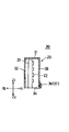
- Patent Document 1 discloses a so-called right-angle USB (Universal Serial Bus) connector 20 as shown in FIGS.
- the USB connector 20 has a metal plate shell formed by folding a metal plate.
- the metal plate shell 23 includes a top plate portion 31 and left and right side plate portions 32. , 33 and the bottom plate portion 34.
- a locking piece 36 extending from the bottom plate portion 34 locks the outer surface of the right side plate portion 33.
- Patent Document 1 has room for improvement in suppressing material costs.
- An object of the present invention is to provide a connector in which material costs are reduced.
- a right angle type connector that includes a contact, a housing that holds the contact, and a shell that covers the housing and is used by being mounted on a board is configured as follows. ing. That is, the shell has a soldered terminal portion connected to the substrate.
- the solder terminal portion has a first solder terminal portion and a second solder terminal portion.
- the first soldered terminal portion is formed to extend from the first side wall portion that is folded back from the front surface of the housing in which a coupling hole into which the mating connector is inserted is formed toward the substrate side.
- the second solder terminal portion extends from the upper side wall portion folded from the front surface toward the upper surface of the housing toward the substrate side from the second side wall portion folded toward the side surface of the housing. It is formed.
- the side surface of the housing is covered by the first side wall and the second side wall.
- the above connector is further configured as follows. That is, the shell has a front wall portion provided on the front side of the housing.
- the above connector is further configured as follows. That is, the shell has a contact portion that can come into contact with the substrate when a torque that moves the second side wall portion away from the substrate acts on the housing.
- the above connector is further configured as follows. That is, the contact portion is formed by being folded back from the front surface of the housing toward the side surface.
- the above connector is further configured as follows. That is, the housing is formed so as to be able to come into contact with the substrate when a torque for moving the second side wall portion away from the substrate acts on the housing.
- the above connector is further configured as follows. That is, the back surface of the housing is formed so as to be able to contact the substrate when a torque is applied to the housing to move the second side wall portion away from the substrate.
- the first side wall portion having the first soldered terminal portion that covers the side surface of the housing and the second side wall portion having the second soldered terminal portion do not overlap each other.
- a connector with reduced cost can be provided.
- FIG. 2 of Patent Document 1 FIG. 3 of Patent Document 1
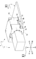
- the modular connector 1 is for connecting a cable such as a LAN (Local Area Network) cable to the board 2, for example, a modular jack 3 (connector) mounted on the board 2 and a modular attached to the cable. And a plug 4 (a mating connector).
- the modular plug 4 is coupled to the modular jack 3 so that the cable is connected to the substrate 2.
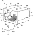
- the modular jack 3 includes a plurality of contacts 5, a housing 6 that holds the plurality of contacts 5 (see also FIG. 5), and a shell 7 that covers the housing 6 (see also FIG. 6). .
- the modular jack 3 is used by being mounted on the board 2 as shown in FIGS. 1 and 2, and as shown in the figure, the right angle type (the coupling direction of the female connector and the male connector with respect to the board is determined). In the horizontal direction, the terminal portion attached to the board is bent toward the board).
- the insertion direction of the modular plug 4 with respect to the modular jack 3 is defined as a direction Y1
- the opposite direction to the direction Y1 is defined as a direction Y0
- directions that are orthogonal to the directions Y1 and Y0 and parallel to the surface direction of the main surface of the substrate 2 are defined as a direction X0 and a direction X1.
- the directions perpendicular to the direction Y1, the direction Y0, the direction X0, and the direction X1, that is, the normal direction of the main surface of the substrate 2 are defined as a direction Z0 and a direction Z1, respectively.
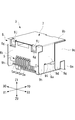
- the housing 6 has a substantially cubic shape and has a front surface 6a, a back surface 6b, an upper surface 6c, a bottom surface 6d, a right side surface 6e, and a left side surface 6f.
- a coupling chamber 8 (coupling hole) into which the modular plug 4 (see also FIG. 1) can be inserted is formed on the front surface 6 a of the housing 6.
- the plurality of contacts 5 held by the housing 6 are formed to protrude from the housing 6 through the back surface 6 b from the inside of the coupling chamber 8. 4 are soldered to the electrode pads 2a of the substrate 2 shown in FIG.
- the modular jack 3 of the present embodiment can be said to be a surface mount type.
- the shell 7 shown in FIG. 6 covers the housing 6 as shown in FIGS. 3 and 4 for the purpose of EMI (Electromagnetic Interference) countermeasures, and the metal plate 9 shown in FIG. It is formed by bending.
- EMI Electromagnetic Interference
- the board 2 shown in FIG. 7 fixes the modular jack 3 to the board 2 and a notch 2 b having a substantially rectangular shape in plan view for accommodating a part of the modular jack 3.
- a fixing hole 2c for this purpose and the electrode pad 2a described above are formed.
- the plurality of fixing holes 2c are formed so as to sandwich the notch 2b in the directions X0 and X1. Specifically, two fixing holes 2c are formed on the direction X0 side as viewed from the notch 2b of the substrate 2, and two fixing holes 2c are formed on the direction X1 side.
- a copper foil 2d is attached around each fixing hole 2c.
- a slightly narrow substrate insertion portion 6u is formed in the lower portion of the housing 6.
- the substrate insertion portion 6u is inserted into a notch 2b (see also FIG. 7) of the substrate 2 as shown in FIGS.
- a pair of flange portions 6t is provided at the front surface 6a side end portion of the substrate insertion portion 6u in order to ensure a sufficient area of the front surface 6a. Is formed.
- a contact accommodating groove 8b is formed on each inner wall side surface 8a of the coupling chamber 8.
- a pair of fixing grooves 6g is formed at the upper end of the back surface 6b of the housing 6 (see also FIG. 4).
- the metal plate 9 constituting the shell 7 mainly includes a front wall portion 9a, an upper wall portion 9b, a pair of first side wall portions 9c, and a pair of second side wall portions 9d. It has as a configuration.
- an alternate long and short dash line indicates a folded portion.
- the front wall portion 9 a covers the front surface 6 a of the housing 6.
- the front wall 9a has a pair of grounding contacts 9f for grounding the coupling hole 9e corresponding to the contour shape of the coupling chamber 8 (see FIG. 5) and the outer shield of the modular plug 4. And are formed.
- the ground contact 9f is folded back into the coupling chamber 8 and partially accommodated in the contact accommodating groove 8b.
- the upper wall portion 9 b is folded at a substantially right angle from the front surface 6 a of the housing 6 toward the upper surface 6 c, and the upper surface 6 c of the housing 6 is It is something to cover.
- the first side wall portion 9 c is folded at a substantially right angle from the front surface 6 a of the housing 6 toward the right side surface 6 e and the left side surface 6 f.
- the second side wall portion 9d is folded at a substantially right angle from the upper surface 6c of the housing 6 toward the right side surface 6e and the left side surface 6f.
- the right side surface 6 e and the left side surface 6 f of the housing 6 are covered by the shell 7 without a gap due to the presence of the first side wall portion 9 c and the second side wall portion 9 d.
- FIGS. 3 the right side surface 6 e and the left side surface 6 f of the housing 6 are covered by the shell 7 without a gap due to the presence of the first side wall portion 9 c and the second side wall portion 9 d.
- the first side wall portion 9 c covers the right side surface 6 e of the housing 6 and the front side 6 a side half of the left side surface 6 f, and the second side wall portion 9 d The right side surface 6e and the back surface 6b side half of the left side surface 6f are covered. Moreover, as shown in FIG.3 and FIG.4, the 1st side wall part 9c and the 2nd side wall part 9d do not mutually overlap at all.
- each of the first solder terminal portions 9g is formed to extend from the first side wall portion 9c in the downward direction in FIG. That is, as shown in FIG. 1, each first soldered terminal portion 9g is formed extending from the first side wall portion 9c toward the substrate 2 and penetrates the fixing hole 2c.
- each second soldered terminal portion 9h is formed to extend from the second side wall portion 9d in the left-right direction on the paper surface. That is, as shown in FIG. 1, each second soldered terminal portion 9h is formed to extend from the second side wall portion 9d toward the substrate 2 and penetrates the fixing hole 2c.
- the soldered terminal portion 7a of the shell 7 is constituted by the first soldered terminal portion 9g and the second soldered terminal portion 9h as shown in FIG.
- the first soldering terminal portion 9g and the second soldering terminal portion 9h are soldered to the substrate 2 via the copper foil 2d while being inserted into the fixing hole 2c of the substrate 2 as shown in FIG. Is done.
- claw part 9i is formed in the vicinity of each 2nd soldering terminal part 9h.
- claw part 9i is return
- a pair of second claw portions 9j are formed on the opposite side of the front wall portion 9a with the upper wall portion 9b interposed therebetween.
- Each second claw portion 9j is folded inward as shown in FIGS. 4 and 6 and is received in the fixing groove 6g (see FIG. 4) of the housing 6.
- claw part 9k is formed in the opposite side to the upper wall part 9b on both sides of the front wall part 9a.
- claw part 9k is return
- first claw portion 9i, second claw portion 9j, and third claw portion 9k fix the shell 7 to the housing 6 and effectively prevent the shell 7 from being lifted from the housing 6.
- the contact part 9m is formed in the vicinity of each 1st side wall part 9c.
- Each contact portion 9m is folded back from the front surface 6a of the housing 6 toward the right side surface 6e and the left side surface 6f, as shown in FIGS. 3 and 6, similarly to the first side wall portion 9c.
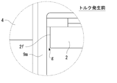
- a gap g of, for example, about 1 mm is formed between the contact portion 9m and the end surface 2f of the substrate 2 as shown in FIG.
- the abutting portion 9m is formed so as to be very close to the end face 2f of the substrate 2 when the modular jack 3 is mounted on the substrate 2.
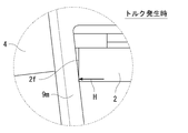
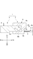
- FIGS. 9, 10A, and 10B The functional role of the contact portion 9m will be described with reference to FIGS. 9, 10A, and 10B.
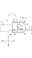
- the modular plug 4 is pushed and squeezed with a strong force F toward the lower side of the drawing.
- the torque T in the counterclockwise direction in the drawing is generated in the modular connector 1.
- the torque T works to keep the second side wall portion 9d away from the substrate 2.
- the second solder terminal portion 9h since the second solder terminal portion 9h is soldered to the fixing hole 2c, the second solder terminal portion 9h functions to keep the second side wall portion 9d away from the substrate 2.
- the second soldering terminal portion 9h is formed by being folded back from the upper wall portion 9b via the second side wall portion 9d, the second soldering terminal portion 9h and the upper wall portion 9b can The strength in the direction in which the two side wall portions 9d are opened is strong, and the strength of the modular connector 1 with respect to the substrate 2 can be improved.
- the shell 7 shown in FIG. 9 is slightly deformed counterclockwise on the paper surface, and the gap g between the abutting portion 9m shown in FIG. As shown in FIG. 10B, it disappears and the contact portion 9m hits the end surface 2f of the substrate 2 and comes into contact therewith. Then, this physical contact generates a reaction force H (see FIG. 10B) that cancels out a part of the torque T shown in FIG. Therefore, the presence of the contact portion 9m can reduce the burden on the second soldered terminal portion 9h when the modular plug 4 is pushed and squeezed with a strong force F as shown in FIG.
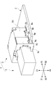
- FIG. 11 schematically shows the modular plug 4, the housing 6 of the modular jack 3, and the substrate 2.
- the back surface 6 b of the housing 6 is formed so as to come into contact with the end surface 2 g of the substrate 2 when the torque T acts on the housing 6.
- the back surface 6b of the housing 6 has a first back surface 6h on the top surface 6c side and a second back surface 6i on the bottom surface 6d side.
- the 2nd back surface 6i is formed so that the end surface 2g of the board
- the second back surface 6i of the back surface 6b of the housing 6 comes into contact with the end surface 2g of the substrate 2 with a strong pressure, and the reaction force I as a reaction force is obtained.
- the second back surface 6 i is received from the end surface 2 g of the substrate 2.
- This reaction force I is offset with a part of the torque T described above. Therefore, the presence of the second back surface 6i reduces the burden on the second soldered terminal portion 9h (see FIG. 9) when the modular plug 4 is pushed and squeezed with a strong force F as shown in FIG. can do.
- the modular jack 3 is configured as follows. That is, as shown in FIG. 3, the shell 7 has a soldered terminal portion 7 a connected to the substrate 2.
- the soldered terminal portion 7a has a first soldered terminal portion 9g and a second soldered terminal portion 9h.
- the first soldered terminal portion 9g is formed on the substrate 2 from the first side wall portion 9c folded back from the front surface 6a of the housing 6 toward the right side surface 6e and the left side surface 6f (see FIG. 1). ) Side.
- FIGS. 1 Side
- the second soldered terminal portion 9 h extends from the upper wall portion 9 b folded from the front surface 6 a to the upper surface 6 c of the housing 6 toward the right side surface 6 e and the left side surface 6 f of the housing 6.
- the second side wall portion 9d folded back is formed to extend toward the substrate 2 (see FIG. 1).
- the first side wall portion 9c and the second side wall portion 9d cover the right side surface 6e and the left side surface 6f of the housing 6. That is, as shown in FIG. 15, the metal plate shell 23 of the USB connector 20 of the cited document 1 had an overlapping portion as can be seen from the positional relationship between the reference numerals 36 (37) and 33.
- the total area of the metal plate 9 (see FIG. 8), which is the material of the shell 7, can be suppressed.
- the modular jack 3 in which the material cost is suppressed can be provided.
- the modular jack 3 is attached to the board 2 at two places on one side, so that the modular jack 3 is firmly fixed to the board 2.
- the shell 7 contacts the substrate 2 when the torque T that tries to move the second side wall portion 9 d away from the substrate 2 acts on the housing 6. It has a possible contact portion 9m.
- the contact portion 9m can contact the substrate 2 when the torque T is generated, a part of the torque T is offset. Since part of the torque T is offset, the burden on the second solder terminal 9h that keeps the second side wall 9d away from the substrate 2 can be reduced.
- the housing 6 abuts against the substrate 2 when a torque T to move the second side wall portion 9d (see FIG. 9) away from the substrate 2 acts on the housing 6. It is made possible. In this way, by adopting a configuration in which the housing 6 can come into contact with the substrate 2 when the torque T is generated, a part of the torque T is offset. Since part of the torque T is offset, the burden on the second solder terminal 9h that keeps the second side wall 9d away from the substrate 2 can be reduced.
- the soldered portions of the first soldered terminal portion 9g and the second soldered terminal portion 9h with the substrate 2 pass through the fixing holes 2c of the substrate 2, respectively. Are extended from the first side wall portion 9c and the second side wall portion 9d, respectively.
- the fixing hole 2 c is not formed in the substrate 2. Therefore, the lower end portion of the first soldering terminal portion 9g is folded outward at a substantially right angle so that the soldering portion 9p parallel to the substrate 2 and the lower end portion of the second soldering terminal portion 9h are folded outward at a substantially right angle.
- soldering portions 9q that are parallel to the substrate 2 are formed, and the soldering portions 9p and the soldering portions 9q are respectively soldered to the copper foil 2d of the substrate 2.
- first soldered terminal portion 9g and the second soldered terminal portion 9h in the present embodiment are also directed from the first side wall portion 9c and the second side wall portion 9d toward the substrate 2, respectively, as in the first embodiment. It is extended and formed.
- the shell 7 has a rear wall portion 9r that partially covers the back surface 6b of the housing 6, as shown in FIG.
- the rear wall portion 9r is formed by being folded back from the upper surface 6c of the housing 6 shown in FIG. 5 toward the back surface 6b of the housing 6 shown in FIG. According to the presence of the rear wall portion 9r, the housing 6 is covered by the shell 7 in a wider range than the first embodiment shown in FIG. More powerful.
Landscapes
- Details Of Connecting Devices For Male And Female Coupling (AREA)
- Coupling Device And Connection With Printed Circuit (AREA)
Abstract
Description
以下、図1~図11を参照しつつ、本願発明の第1実施形態に係るモジュラージャックを説明する。
ハウジング6の下部には若干幅狭な基板挿入部6uが形成されている。この基板挿入部6uは、図1や図2に示すように基板2の切り欠き2b(図7を併せて参照)内に挿入される。また、図5に示すように、幅狭な基板挿入部6uを形成する一方で、前面6aの面積を十分に確保すべく、基板挿入部6uの前面6a側端部には一対の鍔部6tが形成されている。
シェル7を構成する金属製板9は、図8に示すように、前壁部9aと、上壁部9bと、一対の第1側壁部9cと、一対の第2側壁部9dと、を主たる構成として有している。図8において、一点鎖線は折り返しの箇所を示している。
(1)以上説明したように上記実施形態においてモジュラージャック3は、以下のように構成されている。即ち、図3に示すように、シェル7は、基板2に対して接続される半田付端子部7aを有する。半田付端子部7aは、第1半田付端子部9gと第2半田付端子部9hを有する。第1半田付端子部9gは、図3及び図5に示すように、ハウジング6の前面6aから右側面6e、左側面6fに向かって折り返された第1側壁部9cから基板2(図1参照)側に向かって延びて形成されている。第2半田付端子部9hは、図3及び図5に示すように、ハウジング6の前面6aから上面6cに向かって折り返された上壁部9bからハウジング6の右側面6e、左側面6fに向かって折り返された第2側壁部9dから基板2(図1参照)側に向かって延びて形成されている。そして、図3及び図5に示すように、第1側壁部9cと第2側壁部9dにより、ハウジング6の右側面6e、左側面6fが覆われている。即ち、図15に示すように、引用文献1のUSBコネクタ20の金属板製シェル23には符号36(37)と符号33の位置関係から判る通り、重なり合う部分があった。これに対し、上記の構成によれば、図3に示すように、シェル7に重なり合う部分がないのでシェル7の素材である金属製板9(図8参照)の総面積が抑えられ、もって、材料費の抑制が図られたモジュラージャック3を提供することができる。
次に、図12を参照しつつ、本願発明の第2実施形態に係るモジュラージャック3を説明する。以下、本実施形態が上記第1実施形態と相違する点を中心に説明し、重複する説明は適宜、割愛する。また、上記第1実施形態で説明した構成要素に対応する構成要素には原則として同一の符号を付すこととする。
次に、図13を参照しつつ、本願発明の第3実施形態に係るモジュラージャック3を説明する。以下、本実施形態が上記第1実施形態と相違する点を中心に説明し、重複する説明は適宜、割愛する。また、上記第1実施形態で説明した構成要素に対応する構成要素には原則として同一の符号を付すこととする。
2 基板
3 モジュラージャック(コネクタ)
4 モジュラープラグ(相手側コネクタ)
5 コンタクト
6 ハウジング
6a 前面
6b 背面
6c 上面
6d 底面
6e 右側面
6f 左側面
7 シェル
7a 半田付端子部
8 結合室
9 金属製板
9a 前壁部
9b 上壁部
9c 第1側壁部
9d 第2側壁部
9e 結合孔
9f 接地用コンタクト
9g 第1半田付端子部
9h 第2半田付端子部
9m 当接部
9r 後壁部
T トルク
Claims (5)
- コンタクトと、前記コンタクトを保持するハウジングと、前記ハウジングを覆うシェルと、を有し、基板に搭載されて用いられるライトアングルタイプのコネクタであって、
前記シェルは、前記基板に対して接続される半田付端子部を有し、
前記半田付端子部は、第1半田付端子部と第2半田付端子部を有し、
前記第1半田付端子部は、相手側コネクタが挿入される結合孔が形成される前記ハウジングの前面から側面に向かって折り返された第1側壁部から前記基板側に向かって延びて形成され、
前記第2半田付端子部は、前記ハウジングの前記前面から上面に向かって折り返された上壁部から前記ハウジングの前記側面に向かって折り返された第2側壁部から前記基板側に向かって延びて形成され、
前記第1側壁部と前記第2側壁部により、前記ハウジングの前記側面が覆われている、
ことを特徴とするコネクタ。 - 請求項1に記載のコネクタであって、
前記シェルは、前記ハウジングの前記前面側に設けられる前壁部と、
前記第2側壁部を前記基板から遠ざけようとするトルクが前記ハウジングに作用した際に前記基板と当接可能な当接部を有する、
ことを特徴とするコネクタ。 - 請求項2に記載のコネクタであって、
前記当接部は、前記ハウジングの前記前面から前記側面に向かって折り返されて形成される、
ことを特徴とするコネクタ。 - 請求項1~3の何れかに記載のコネクタであって、
前記ハウジングは、前記第2側壁部を前記基板から遠ざけようとするトルクが前記ハウジングに作用した際に、前記基板と当接可能に形成されている、
ことを特徴とするコネクタ。 - 請求項4に記載のコネクタであって、
前記ハウジングの前記背面が、前記第2側壁部を前記基板から遠ざけようとするトルクが前記ハウジングに作用した際に、前記基板と当接可能に形成されている、
ことを特徴とするコネクタ。
Priority Applications (3)
| Application Number | Priority Date | Filing Date | Title |
|---|---|---|---|
| KR1020127023421A KR101336656B1 (ko) | 2010-03-19 | 2010-11-30 | 커넥터 |
| US13/521,634 US8708744B2 (en) | 2010-03-19 | 2010-11-30 | Electrical connector having shield with soldered terminal portions |
| CN201080065554XA CN102812600A (zh) | 2010-03-19 | 2010-11-30 | 连接器 |
Applications Claiming Priority (2)
| Application Number | Priority Date | Filing Date | Title |
|---|---|---|---|
| JP2010064504A JP4704504B1 (ja) | 2010-03-19 | 2010-03-19 | コネクタ |
| JP2010-064504 | 2010-03-19 |
Publications (1)
| Publication Number | Publication Date |
|---|---|
| WO2011114402A1 true WO2011114402A1 (ja) | 2011-09-22 |
Family
ID=44237105
Family Applications (1)
| Application Number | Title | Priority Date | Filing Date |
|---|---|---|---|
| PCT/JP2010/006975 Ceased WO2011114402A1 (ja) | 2010-03-19 | 2010-11-30 | コネクタ |
Country Status (5)
| Country | Link |
|---|---|
| US (1) | US8708744B2 (ja) |
| JP (1) | JP4704504B1 (ja) |
| KR (1) | KR101336656B1 (ja) |
| CN (1) | CN102812600A (ja) |
| WO (1) | WO2011114402A1 (ja) |
Families Citing this family (4)
| Publication number | Priority date | Publication date | Assignee | Title |
|---|---|---|---|---|
| US9437947B2 (en) * | 2013-11-27 | 2016-09-06 | Fci Americas Technology Llc | Electrical connector having hold down member |
| US10276989B2 (en) * | 2016-12-19 | 2019-04-30 | Foxconn Interconnect Technology Limited | Electrical connector with intimate side arms extending from metallic shell and integrally formed within insulative shell |
| JP7558032B2 (ja) * | 2020-10-28 | 2024-09-30 | 日本航空電子工業株式会社 | アンテナ及び組立体 |
| JP2024081178A (ja) * | 2022-12-06 | 2024-06-18 | 株式会社オートネットワーク技術研究所 | コネクタ装置 |
Citations (2)
| Publication number | Priority date | Publication date | Assignee | Title |
|---|---|---|---|---|
| JP2004515890A (ja) * | 2000-12-06 | 2004-05-27 | パルス エンジニアリング | シールド型超小形電子コネクタ・アセンブリおよびその製造方法 |
| JP2007115707A (ja) * | 2006-12-18 | 2007-05-10 | Taiko Denki Co Ltd | レセプタクル |
Family Cites Families (28)
| Publication number | Priority date | Publication date | Assignee | Title |
|---|---|---|---|---|
| JPH0313682U (ja) * | 1989-06-26 | 1991-02-12 | ||
| JPH0332378U (ja) * | 1989-08-07 | 1991-03-28 | ||
| US5288248A (en) * | 1991-10-28 | 1994-02-22 | Foxconn International | Totally shielded DIN connector |
| US5637014A (en) * | 1994-01-31 | 1997-06-10 | Mitsumi Electric Co., Ltd. | Electrical connector |
| US5637015A (en) * | 1995-08-31 | 1997-06-10 | Hon Hai Precision Ind. Co., Ltd. | Shielded electrical connector |
| TW321372U (en) * | 1997-05-16 | 1997-11-21 | Molex Taiwan Co Ltd | Electrical connector to block the EMI (Electromagnetic Interference) |
| EP1021853A4 (en) * | 1997-10-10 | 2001-01-10 | Stewart Connector Systems | MULTIPLE JACKET FOR HIGH FREQUENCIES WITH TWO MOVED ACCESS LEVELS |
| TW371525U (en) * | 1998-04-09 | 1999-10-01 | Molex Taiwan Ltd | Connector wrapping device |
| JP2000357550A (ja) | 1999-06-15 | 2000-12-26 | Fujitsu Takamisawa Component Ltd | 金属板を折り込んで形成された金属板製シェルを有するコネクタ |
| US6682368B2 (en) * | 2000-05-31 | 2004-01-27 | Tyco Electronics Corporation | Electrical connector assembly utilizing multiple ground planes |
| US6475033B1 (en) * | 2001-10-10 | 2002-11-05 | Hon Hai Precision Ind. Co., Ltd. | Electrical connector |
| JP2004014350A (ja) * | 2002-06-07 | 2004-01-15 | Japan Aviation Electronics Industry Ltd | コネクタ |
| TW547852U (en) * | 2002-10-04 | 2003-08-11 | Hon Hai Prec Ind Co Ltd | Low profile connector |
| US7217146B2 (en) * | 2004-12-17 | 2007-05-15 | Scientific-Atlanta, Inc. | Connector insert for preventing contamination |
| US7097507B1 (en) * | 2005-06-02 | 2006-08-29 | Hon Hai Precision Ind. Co., Ltd. | Electrical connector with improved shell |
| CN2886841Y (zh) * | 2006-01-24 | 2007-04-04 | 富士康(昆山)电脑接插件有限公司 | 电连接器 |
| US7744418B2 (en) * | 2006-07-18 | 2010-06-29 | Hon Hai Precision Ind. Co., Ltd. | Upright electrical connector |
| TWM330608U (en) * | 2007-11-16 | 2008-04-11 | Wonten Technology Co Ltd | Electric connector |
| US7645165B2 (en) * | 2008-03-17 | 2010-01-12 | Hon Hai Precision Ind. Co., Ltd. | Electrical connector with improved shielding shell |
| JP5080336B2 (ja) * | 2008-04-04 | 2012-11-21 | 日本航空電子工業株式会社 | 基板実装用コネクタ |
| TWM357044U (en) * | 2008-12-03 | 2009-05-11 | Advanced Connectek Inc | Insulating body and electrical connector therewith |
| CN201360060Y (zh) * | 2008-12-22 | 2009-12-09 | 上海莫仕连接器有限公司 | 电连接器 |
| US7731534B1 (en) * | 2008-12-29 | 2010-06-08 | Cheng Uei Precision Industry Co., Ltd. | Electrical connector with improved buckling tab |
| CN201378666Y (zh) * | 2009-03-09 | 2010-01-06 | 丽洋科技股份有限公司 | 一种rj45连接器 |
| US7833057B1 (en) * | 2009-06-08 | 2010-11-16 | Cheng Uei Precision Industry Co., Ltd. | Receptacle connector |
| JP5614955B2 (ja) * | 2009-08-07 | 2014-10-29 | ホシデン株式会社 | レセプタクルコネクタ |
| JP5285533B2 (ja) * | 2009-08-07 | 2013-09-11 | ホシデン株式会社 | コネクタ及び電子機器 |
| JP5622306B2 (ja) * | 2010-07-05 | 2014-11-12 | 矢崎総業株式会社 | 基板搭載型コネクタ |
-
2010
- 2010-03-19 JP JP2010064504A patent/JP4704504B1/ja not_active Expired - Fee Related
- 2010-11-30 WO PCT/JP2010/006975 patent/WO2011114402A1/ja not_active Ceased
- 2010-11-30 KR KR1020127023421A patent/KR101336656B1/ko not_active Expired - Fee Related
- 2010-11-30 US US13/521,634 patent/US8708744B2/en not_active Expired - Fee Related
- 2010-11-30 CN CN201080065554XA patent/CN102812600A/zh active Pending
Patent Citations (2)
| Publication number | Priority date | Publication date | Assignee | Title |
|---|---|---|---|---|
| JP2004515890A (ja) * | 2000-12-06 | 2004-05-27 | パルス エンジニアリング | シールド型超小形電子コネクタ・アセンブリおよびその製造方法 |
| JP2007115707A (ja) * | 2006-12-18 | 2007-05-10 | Taiko Denki Co Ltd | レセプタクル |
Also Published As
| Publication number | Publication date |
|---|---|
| KR101336656B1 (ko) | 2013-12-04 |
| JP4704504B1 (ja) | 2011-06-15 |
| US8708744B2 (en) | 2014-04-29 |
| US20130017734A1 (en) | 2013-01-17 |
| KR20120125362A (ko) | 2012-11-14 |
| CN102812600A (zh) | 2012-12-05 |
| JP2011198633A (ja) | 2011-10-06 |
Similar Documents
| Publication | Publication Date | Title |
|---|---|---|
| US8882542B2 (en) | Electrical connection device | |
| JP5723980B2 (ja) | 多重使用電気コネクタ | |
| JP4613235B2 (ja) | コネクタ | |
| JP2013026155A (ja) | 防水コネクタ用端子 | |
| JP4704504B1 (ja) | コネクタ | |
| CN104979684A (zh) | 插座连接器 | |
| JP4828626B2 (ja) | コネクタ | |
| US7438595B2 (en) | Small-sized electrical connector easily improved in EMI characteristics | |
| JP4082707B2 (ja) | コネクタ | |
| CN101728686A (zh) | 连接器 | |
| CN210182658U (zh) | 全屏蔽小间距板对板连接器 | |
| JP2010157367A (ja) | 電気コネクタ | |
| JP7176372B2 (ja) | 端子 | |
| JP5956720B2 (ja) | 電気コネクタ | |
| JP5473073B2 (ja) | レセプタクルのシールドケース | |
| JP5498848B2 (ja) | コネクタ | |
| WO2014148134A1 (ja) | Usb規格準拠レセプタクルコネクタ | |
| JP7392283B2 (ja) | 電気コネクタ | |
| JP6525030B2 (ja) | コネクタハウジング、コネクタ、及びコネクタユニット | |
| CN205752653U (zh) | 电连接器 | |
| JP5794715B2 (ja) | コネクタ | |
| JP5660925B2 (ja) | コネクタ | |
| JP4675768B2 (ja) | フラットケーブル用端子 | |
| JP6406705B2 (ja) | コンタクト、リセプタクル及びコネクタ | |
| TW202301748A (zh) | 板端連接器 |
Legal Events
| Date | Code | Title | Description |
|---|---|---|---|
| WWE | Wipo information: entry into national phase |
Ref document number: 201080065554.X Country of ref document: CN |
|
| 121 | Ep: the epo has been informed by wipo that ep was designated in this application |
Ref document number: 10847820 Country of ref document: EP Kind code of ref document: A1 |
|
| WWE | Wipo information: entry into national phase |
Ref document number: 13521634 Country of ref document: US |
|
| ENP | Entry into the national phase |
Ref document number: 20127023421 Country of ref document: KR Kind code of ref document: A |
|
| NENP | Non-entry into the national phase |
Ref country code: DE |
|
| 122 | Ep: pct application non-entry in european phase |
Ref document number: 10847820 Country of ref document: EP Kind code of ref document: A1 |