WO2011108533A1 - 半導体素子基板の製造方法 - Google Patents
半導体素子基板の製造方法 Download PDFInfo
- Publication number
- WO2011108533A1 WO2011108533A1 PCT/JP2011/054610 JP2011054610W WO2011108533A1 WO 2011108533 A1 WO2011108533 A1 WO 2011108533A1 JP 2011054610 W JP2011054610 W JP 2011054610W WO 2011108533 A1 WO2011108533 A1 WO 2011108533A1
- Authority
- WO
- WIPO (PCT)
- Prior art keywords
- group
- acid
- ene
- resin
- semiconductor element
- Prior art date
- Legal status (The legal status is an assumption and is not a legal conclusion. Google has not performed a legal analysis and makes no representation as to the accuracy of the status listed.)
- Ceased
Links
Images

Classifications
-
- H—ELECTRICITY
- H10—SEMICONDUCTOR DEVICES; ELECTRIC SOLID-STATE DEVICES NOT OTHERWISE PROVIDED FOR
- H10D—INORGANIC ELECTRIC SEMICONDUCTOR DEVICES
- H10D30/00—Field-effect transistors [FET]
- H10D30/01—Manufacture or treatment
- H10D30/021—Manufacture or treatment of FETs having insulated gates [IGFET]
- H10D30/031—Manufacture or treatment of FETs having insulated gates [IGFET] of thin-film transistors [TFT]
- H10D30/0312—Manufacture or treatment of FETs having insulated gates [IGFET] of thin-film transistors [TFT] characterised by the gate electrodes
- H10D30/0316—Manufacture or treatment of FETs having insulated gates [IGFET] of thin-film transistors [TFT] characterised by the gate electrodes of lateral bottom-gate TFTs comprising only a single gate
-
- H—ELECTRICITY
- H10—SEMICONDUCTOR DEVICES; ELECTRIC SOLID-STATE DEVICES NOT OTHERWISE PROVIDED FOR
- H10D—INORGANIC ELECTRIC SEMICONDUCTOR DEVICES
- H10D30/00—Field-effect transistors [FET]
- H10D30/01—Manufacture or treatment
- H10D30/021—Manufacture or treatment of FETs having insulated gates [IGFET]
- H10D30/031—Manufacture or treatment of FETs having insulated gates [IGFET] of thin-film transistors [TFT]
- H10D30/0321—Manufacture or treatment of FETs having insulated gates [IGFET] of thin-film transistors [TFT] comprising silicon, e.g. amorphous silicon or polysilicon
-
- H—ELECTRICITY
- H10—SEMICONDUCTOR DEVICES; ELECTRIC SOLID-STATE DEVICES NOT OTHERWISE PROVIDED FOR
- H10D—INORGANIC ELECTRIC SEMICONDUCTOR DEVICES
- H10D30/00—Field-effect transistors [FET]
- H10D30/60—Insulated-gate field-effect transistors [IGFET]
- H10D30/67—Thin-film transistors [TFT]
- H10D30/6704—Thin-film transistors [TFT] having supplementary regions or layers in the thin films or in the insulated bulk substrates for controlling properties of the device
-
- H—ELECTRICITY
- H10—SEMICONDUCTOR DEVICES; ELECTRIC SOLID-STATE DEVICES NOT OTHERWISE PROVIDED FOR
- H10D—INORGANIC ELECTRIC SEMICONDUCTOR DEVICES
- H10D86/00—Integrated devices formed in or on insulating or conducting substrates, e.g. formed in silicon-on-insulator [SOI] substrates or on stainless steel or glass substrates
- H10D86/40—Integrated devices formed in or on insulating or conducting substrates, e.g. formed in silicon-on-insulator [SOI] substrates or on stainless steel or glass substrates characterised by multiple TFTs
-
- H—ELECTRICITY
- H10—SEMICONDUCTOR DEVICES; ELECTRIC SOLID-STATE DEVICES NOT OTHERWISE PROVIDED FOR
- H10D—INORGANIC ELECTRIC SEMICONDUCTOR DEVICES
- H10D86/00—Integrated devices formed in or on insulating or conducting substrates, e.g. formed in silicon-on-insulator [SOI] substrates or on stainless steel or glass substrates
- H10D86/40—Integrated devices formed in or on insulating or conducting substrates, e.g. formed in silicon-on-insulator [SOI] substrates or on stainless steel or glass substrates characterised by multiple TFTs
- H10D86/451—Integrated devices formed in or on insulating or conducting substrates, e.g. formed in silicon-on-insulator [SOI] substrates or on stainless steel or glass substrates characterised by multiple TFTs characterised by the compositions or shapes of the interlayer dielectrics
-
- H—ELECTRICITY
- H10—SEMICONDUCTOR DEVICES; ELECTRIC SOLID-STATE DEVICES NOT OTHERWISE PROVIDED FOR
- H10D—INORGANIC ELECTRIC SEMICONDUCTOR DEVICES
- H10D86/00—Integrated devices formed in or on insulating or conducting substrates, e.g. formed in silicon-on-insulator [SOI] substrates or on stainless steel or glass substrates
- H10D86/40—Integrated devices formed in or on insulating or conducting substrates, e.g. formed in silicon-on-insulator [SOI] substrates or on stainless steel or glass substrates characterised by multiple TFTs
- H10D86/60—Integrated devices formed in or on insulating or conducting substrates, e.g. formed in silicon-on-insulator [SOI] substrates or on stainless steel or glass substrates characterised by multiple TFTs wherein the TFTs are in active matrices
Definitions
- the present invention relates to a method for manufacturing a semiconductor element substrate in which a hydrogen plasma treatment is performed on a semiconductor layer and a passivation film using an organic material is formed.
- a thin film transistor is a switching element having terminals called a gate electrode, a source electrode, and a drain electrode, and is widely applied to an active element of an active matrix substrate of a display element such as an active matrix liquid crystal display or an organic EL.
- a passivation film made of a silicon nitride film is formed on the surface of a semiconductor element or a semiconductor layer included in the semiconductor element by sputtering, vapor deposition, or CVD. Further, the surface of the semiconductor layer has been treated for the purpose of improving the adhesion between the SiNx film and the semiconductor layer made of a-Si.
- Patent Document 1 discloses that after a hydrogen plasma treatment is performed on a semiconductor layer, a nitrogen plasma treatment is performed to improve the adhesion between the semiconductor layer and the passivation film and reduce the off-leakage current. Yes.
- Patent Document 1 discloses that after a hydrogen plasma treatment is performed on a semiconductor layer, a nitrogen plasma treatment is performed to improve the adhesion between the semiconductor layer and the passivation film and reduce the off-leakage current. Yes.
- Patent Document 1 discloses that after a hydrogen plasma treatment is performed on a semiconductor layer, a nitrogen plasma treatment is performed to improve the adhesion between the semiconductor layer and the passivation film and reduce the off-leakage current.
- an inorganic material for the passivation film as in Patent Document 1, it is necessary to form the film in a state where the material is plasmatized or ionized in a vacuum, the equipment becomes large-scale, and the operation is complicated. There was a problem of becoming.
- Non-Patent Document 1 discloses that an initial off-leakage current can be suppressed by performing plasma treatment using SiNx for a passivation film.
- this semiconductor element substrate is used as an active matrix substrate of a display element, high reliability is required. That is, not only the initial off-leakage current but also the use of the device under severe conditions is required to suppress the off-leakage current and improve the TFT life.
- Patent Document 2 since SiNx has a function of terminating dangling bonds (see, for example, Patent Document 2), the plasma processing in Patent Document 1 and Non-Patent Document 1 does not mainly terminate dangling bonds. It is.
- An object of the present invention is to provide a semiconductor element substrate manufacturing method capable of manufacturing a highly reliable semiconductor element substrate.
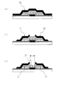
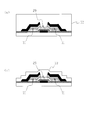
- source / drain electrodes 26 are formed by sputtering.
- the source / drain electrode 26 is patterned by etching as shown in FIG. 2B to form the source electrode 27 and the drain electrode 28. That is, the source electrode 27 and the drain electrode 28 are formed by separating the source / drain electrode 26 by patterning, and the source / drain electrode 26, the source electrode 27, and the drain electrode 28 are all made of the same material.
- the source / drain electrodes are etched by wet etching, but may be dry etching.
- the protic polar group means a group containing an atom in which a hydrogen atom is directly bonded to an atom belonging to Group 15 or Group 16 of the periodic table.
- the atom belonging to group 15 or 16 of the periodic table is preferably an atom belonging to the first or second period of group 15 or 16 of the periodic table, more preferably an oxygen atom, nitrogen atom or sulfur An atom, particularly preferably an oxygen atom.
- protic polar group examples include polar groups having an oxygen atom such as a hydroxyl group, a carboxy group (hydroxycarbonyl group), a sulfonic acid group, and a phosphoric acid group; a primary amino group, a secondary amino group, and a primary group.
- a polar group having a nitrogen atom such as a secondary amide group or a secondary amide group (imide group); a polar group having a sulfur atom such as a thiol group; Among these, those having an oxygen atom are preferable, and a carboxy group is more preferable.
- the cyclic olefin resin is a homopolymer or copolymer of a cyclic olefin monomer having an alicyclic structure and a carbon-carbon double bond.
- the cyclic olefin resin may have a unit derived from a monomer other than the cyclic olefin monomer.
- the proportion of the cyclic olefin monomer unit in the total structural unit of the cyclic olefin resin is usually 30 to 100% by weight, preferably 50 to 100% by weight, more preferably 70 to 100% by weight.
- the protic polar group may be bonded to the cyclic olefin monomer unit or may be bonded to a monomer unit other than the cyclic olefin monomer, It is desirable that it is bonded to a cyclic olefin monomer unit.
- a cyclic olefin monomer having a protic polar group (a), a cyclic olefin monomer having a polar group other than a protic polar group (B), a cyclic olefin monomer having no polar group (c), and a monomer other than the cyclic olefin (d) (these monomers are hereinafter simply referred to as monomers (a) to (d)) .).
- the monomer (d) may have a protic polar group or other polar group, or may not have a polar group at all.
- the cyclic olefin resin having a protic polar group is preferably composed of the monomer (a), the monomer (b) and / or the monomer (c). More preferably, it is composed of (a) and the monomer (b).
- the monomer (a) include 5-hydroxycarbonylbicyclo [2.2.1] hept-2-ene, 5-methyl-5-hydroxycarbonylbicyclo [2.2.1] hept-2-ene. Ene, 5-carboxymethyl-5-hydroxycarbonylbicyclo [2.2.1] hept-2-ene, 5,6-dihydroxycarbonylbicyclo [2.2.1] hept-2-ene, 9-hydroxycarbonyltetra Cyclo [6.2.1.1 3,6 . 0 2,7 ] dodec-4-ene, 9-methyl-9-hydroxycarbonyltetracyclo [6.2.1.1 3,6 .
- cyclic olefin monomers (a) having a protic polar group may be used alone or in combination of two or more.
- ester groups alkoxycarbonyl groups and aryloxycarbonyl groups
- N-substituted imide group epoxy group, halogen atom, cyano group, carbonyloxycarbonyl group (acid anhydride residue of dicarboxylic acid), alkoxy group, carbonyl group, tertiary amino group, sulfone group, acryloyl group Etc.
- an ester group, an N-substituted imide group and a cyano group are preferable, an ester group and an N-substituted imide group are more preferable, and an N-substituted imide group is particularly preferable.
- Specific examples of the monomer (b) include the following cyclic olefins.
- Examples of the cyclic olefin having an ester group include 5-acetoxybicyclo [2.2.1] hept-2-ene, 5-methoxycarbonylbicyclo [2.2.1] hept-2-ene, 5-methyl- 5-methoxycarbonylbicyclo [2.2.1] hept-2-ene, 9-acetoxytetracyclo [6.2.1.1 3,6 . 0 2,7 ] dodec-4-ene, 9-methoxycarbonyltetracyclo [6.2.1.1 3,6 . 0 2,7 ] dodec-4-ene, 9-ethoxycarbonyltetracyclo [6.2.1.1 3,6 .
- dodec-4-ene 9-methyl-9-n-propoxycarbonyltetracyclo [6.2.1.1 3,6 . 0 2,7 ] dodec-4-ene, 9-methyl-9-isopropoxycarbonyltetracyclo [6.2.1.1 3,6 . 0 2,7 ] dodec-4-ene, 9-methyl-9-n-butoxycarbonyltetracyclo [6.2.1.1 3,6 . 0 2,7 ] dodec-4-ene, 9- (2,2,2-trifluoroethoxycarbonyl) tetracyclo [6.2.1.1 3,6 .
- Examples of the cyclic olefin having a halogen atom include 9-chlorotetracyclo [6.2.1.1 3,6 . 0 2,7 ] dodec-4-ene, 9-methyl-9-chlorotetracyclo [6.2.1.1 3,6 . 0 2,7 ] dodec-4-ene and the like.
- cyclic olefin monomers (b) having a polar group other than the protic polar group may be used alone or in combination of two or more.
- cyclic olefin monomer (c) having no polar group examples include bicyclo [2.2.1] hept-2-ene (also referred to as “norbornene”), 5-ethyl-bicyclo [2. 2.1] Hept-2-ene, 5-butyl-bicyclo [2.2.1] hept-2-ene, 5-ethylidene-bicyclo [2.2.1] hept-2-ene, 5-methylidene- Bicyclo [2.2.1] hept-2-ene, 5-vinyl-bicyclo [2.2.1] hept-2-ene, tricyclo [5.2.1.0 2,6 ] deca-3,8 - diene (common name: dicyclopentadiene), tetracyclo [10.2.1.0 2,11.
- cyclic olefin monomers (c) having no polar group may be used alone or in combination of two or more.
- the cyclic olefin resin having a protic polar group used in the present invention introduces a protic polar group into a cyclic olefin resin having no protic polar group using a known modifier, and optionally hydrogenated. It can be obtained also by the method of performing. Hydrogenation may be performed on the polymer before introduction of the protic polar group. Further, the cyclic olefin resin having a protic polar group may be further modified to introduce a protic polar group.
- a polymer having no protic polar group can be obtained by polymerizing the monomers (b) to (d) in any combination.
- the polymerization method for polymerizing the monomer (a) together with a monomer selected from the monomers (b) to (d) as desired may be in accordance with a conventional method, for example, ring-opening polymerization method or An addition polymerization method is employed.
- the hydrogenation of the polymer obtained by polymerizing each monomer is usually performed using a hydrogenation catalyst.
- a hydrogenation catalyst for example, those generally used for hydrogenation of olefin compounds can be used.
- a Ziegler type homogeneous catalyst, a noble metal complex catalyst, a supported noble metal catalyst, and the like can be used.
- the hydrogenation rate of the main chain of the hydrogenated polymer is usually 90% or more, preferably 95% or more, more preferably 98% or more. When the hydrogenation rate is within this range, the resin (A) is particularly excellent in heat resistance and suitable.
- the hydrogenation rate of the resin (A) can be measured by 1 H-NMR spectrum. For example, it can be determined as a ratio of the number of moles of hydrogenated carbon-carbon double bonds to the number of moles of carbon-carbon double bonds before hydrogenation.
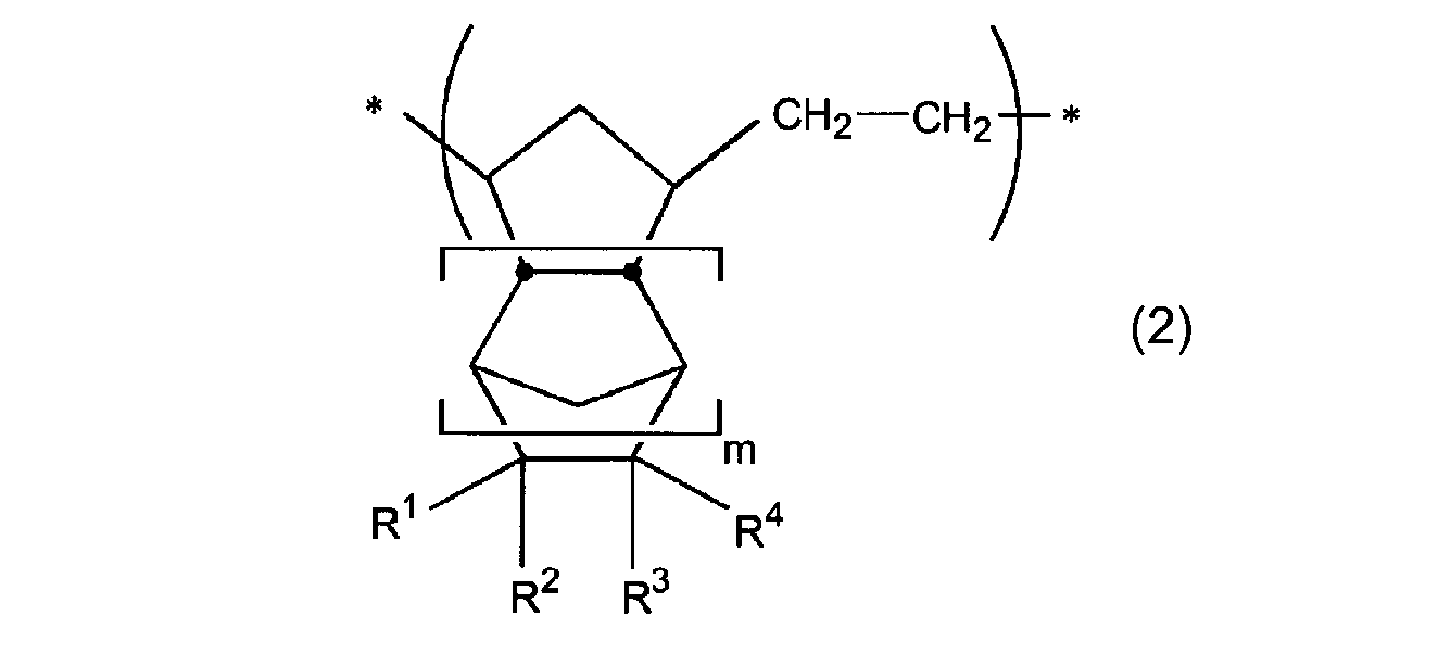
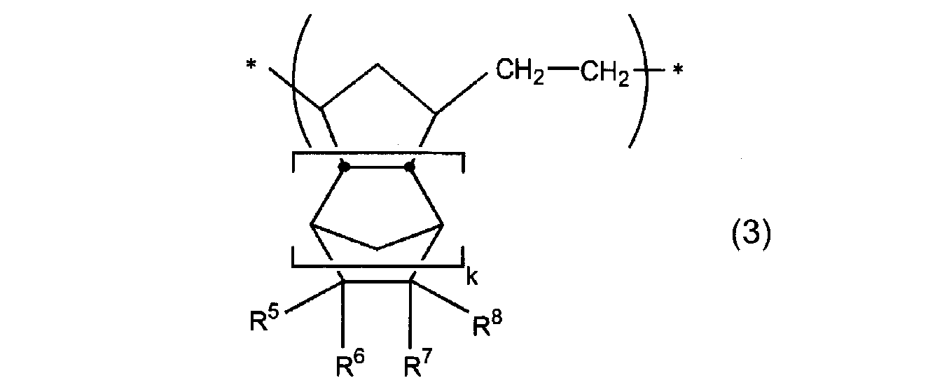
- a resin having a structural unit represented by the formula (2) as shown below is particularly suitable, and a structure represented by the formula (2). What has a unit and the structural unit represented by Formula (3) is more suitable.
- R 1 to R 4 each independently represents a hydrogen atom or a —X n —R ′ group
- X is a divalent organic group; n is 0 or 1; R ′ Is an alkyl group which may have a substituent, an aromatic group which may have a substituent, or a protic polar group.
- At least one of R 1 to R 4 is a —X n —R ′ group where R ′ is a protic polar group.
- m is an integer of 0-2.
- the alkyl group which may have a substituent represented by R ′ is usually a linear or branched alkyl group having 1 to 7 carbon atoms, and examples thereof include a methyl group, an ethyl group, n -Propyl group, isopropyl group and the like.
- the aromatic group which may have a substituent is usually an aromatic group having 6 to 10 carbon atoms, and examples thereof include a phenyl group and a benzyl group.
- the acrylic resin used in the present invention is not particularly limited, but it is a single weight having at least one selected from a carboxylic acid having an acrylic group, a carboxylic acid anhydride having an acrylic group, or an epoxy group-containing acrylate compound as a monomer.
- a blend or copolymer is preferred.
- (meth) acrylic acid, maleic anhydride, glycidyl methacrylate, methacrylic acid-6,7-epoxyheptyl and the like are preferable.
- “(meth)” means either methacryl or acryl.
- acrylate monomers include methyl (meth) acrylate, isopropyl (meth) acrylate, butyl (meth) acrylate, t-butyl (meth) acrylate, ethylhexyl (meth) acrylate, decyl (meth) acrylate, dodecyl ( Alkyl (meth) acrylates such as meth) acrylate, lauryl (meth) acrylate, stearyl (meth) acrylate; hydroxyethyl (meth) acrylate, 2-hydroxypropyl (meth) acrylate, 3-hydroxypropyl (meth) acrylate, etc.
- Hydroxyalkyl (meth) acrylates phenoxyalkyl (meth) acrylates such as phenoxyethyl (meth) acrylate and 2-hydroxy-3-phenoxypropyl (meth) acrylate; Alkoxyalkyl (meth) acrylates such as xylethyl (meth) acrylate and 2-ethoxyethyl (meth) acrylate; polyethylene glycol mono (meth) acrylate, ethoxydiethylene glycol (meth) acrylate, methoxypolyethylene glycol (meth) acrylate, phenoxy polyethylene glycol Polyalkylene glycol (meth) acrylates such as (meth) acrylate; cyclohexyl (meth) acrylate, 4-butylcyclohexyl (meth) acrylate, dicyclopentanyl (meth) acrylate, dicyclopentenyl (meth) acrylate, dicyclopenta Dienyl (meth
- the cardo resin is a resin having a cardo structure, that is, a skeleton structure in which two cyclic structures are bonded to a quaternary carbon atom constituting the cyclic structure.
- a common cardo structure is a fluorene ring bonded to a benzene ring.
- skeleton structure in which two cyclic structures are bonded to a quaternary carbon atom constituting the cyclic structure include a fluorene skeleton, a bisphenol fluorene skeleton, a bisaminophenyl fluorene skeleton, a fluorene skeleton having an epoxy group, and an acrylic group. And a fluorene skeleton having the same.
- Monomers having a cardo structure include, for example, bis (glycidyloxyphenyl) fluorene type epoxy resin; condensate of bisphenolfluorene type epoxy resin and acrylic acid; 9,9-bis (4-hydroxyphenyl) fluorene, Cardio structure-containing bisphenols such as 9-bis (4-hydroxy-3-methylphenyl) fluorene; 9,9-bis (cyanoalkyl) fluorenes such as 9,9-bis (cyanomethyl) fluorene; -9,9-bis (aminoalkyl) fluorenes such as bis (3-aminopropyl) fluorene;
- the cardo resin is a polymer obtained by polymerizing a monomer having a cardo structure, but may be a copolymer with other copolymerizable monomers.
- the polymerization method of the monomer may be according to a conventional method.
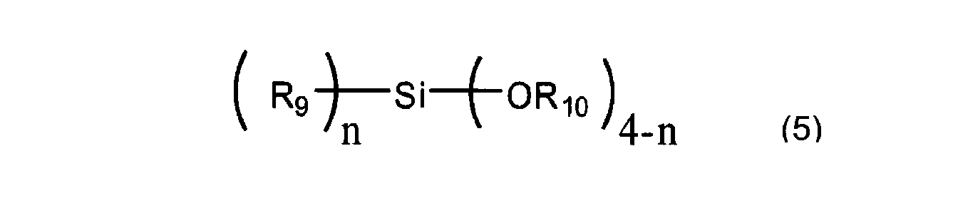
- the structure of the polysiloxane used in the present invention is not particularly limited, but preferably includes a polysiloxane obtained by mixing and reacting at least one organosilane represented by the formula (5).
- R 9 in Formula (5) represents any one of hydrogen, an alkyl group having 1 to 10 carbon atoms, an alkenyl group having 2 to 10 carbon atoms, and an aryl group having 6 to 15 carbon atoms, and a plurality of R 9 are the same. It can be different.
- these alkyl groups, alkenyl groups, and aryl groups may all have a substituent, or may be unsubstituted without a substituent, and are selected according to the characteristics of the composition. it can.
- alkyl group examples include methyl group, ethyl group, n-propyl group, isopropyl group, n-butyl group, t-butyl group, n-hexyl group, n-decyl group, trifluoromethyl group, 2,2 , 2-trifluoroethyl group, 3,3,3-trifluoropropyl group, 3-glycidoxypropyl group, 2- (3,4-epoxycyclohexyl) ethyl group, 3-aminopropyl group, 3-mercaptopropyl Group, 3-isocyanatopropyl group.
- alkenyl group examples include a vinyl group, a 3-acryloxypropyl group, and a 3-methacryloxypropyl group.
- aryl group examples include phenyl, tolyl, p-hydroxyphenyl, 1- (p-hydroxyphenyl) ethyl, 2- (p-hydroxyphenyl) ethyl, 4-hydroxy-5- (p -Hydroxyphenylcarbonyloxy) pentyl group, naphthyl group.
- R 10 is hydrogen of the formula (5), an alkyl group having 1 to 6 carbon atoms, an acyl group having 1 to 6 carbon atoms, or an aryl group having 6 to 15 carbon atoms, even more R 10 is the same as each It may be different.
- these alkyl groups and acyl groups may have a substituent or may be an unsubstituted form having no substituent, and can be selected according to the characteristics of the composition.
- Specific examples of the alkyl group include a methyl group, an ethyl group, an n-propyl group, an isopropyl group, and an n-butyl group.
- Specific examples of the acyl group include an acetyl group.
- aryl group examples include a phenyl group.
- N in the formula (5) represents an integer of 0 to 3.
- organosilanes trifunctional silanes are preferably used from the viewpoint of crack resistance and hardness of the resin film obtained from the resin composition of the present invention. These organosilanes may be used alone or in combination of two or more.
- the polysiloxane in the present invention can be obtained by hydrolyzing and partially condensing the above organosilane.
- a general method can be used for hydrolysis and partial condensation. For example, a solvent, water and, if necessary, a catalyst are added to the mixture, and the mixture is heated and stirred. During stirring, if necessary, hydrolysis by-products (alcohols such as methanol) and condensation by-products (water) may be distilled off by distillation.
- the polyimide used in the present invention can be obtained by heat-treating a polyimide precursor obtained by reacting tetracarboxylic anhydride and diamine.
- a polyimide precursor obtained by reacting tetracarboxylic anhydride and diamine.
- the precursor for obtaining the polyimide resin include polyamic acid, polyamic acid ester, polyisoimide, and polyamic acid sulfonamide.
- the polyimide used in the present invention is synthesized by a known method. That is, a tetracarboxylic dianhydride and a diamine are selectively combined, and these are combined with N-methyl-2-pyrrolidone, N, N-dimethylacetamide, N, N-dimethylformamide, dimethyl sulfoxide, hexamethylphosphorotriamide, It is synthesized by a known method such as reacting in a polar solvent such as ⁇ -butyrolactone and cyclopentanone.
- the resin containing the monomer unit (e) represented by the general formula (1) used in the present invention is a unit obtained by polymerizing a monomer represented by the following general formula (1) ( It is a cyclic olefin resin comprising e).
- R 1 represents a branched alkyl group having 5 to 16 carbon atoms.
- R 1 is a branched alkyl group having 5 to 16 carbon atoms, such as 1-methylbutyl group, 2-methylbutyl group, 1-methylpentyl group, 1-ethylbutyl group, 2-methyl. Examples include hexyl group, 2-ethylhexyl group, 4-methylheptyl group, 1-methylnonyl group, 1-methyltridecyl group, 1-methyltetradecyl group and the like.
- a branched alkyl group having 6 to 14 carbon atoms is preferable, and a branched alkyl group having 7 to 10 carbon atoms is more preferable because of excellent heat resistance and solubility in an organic solvent.
- the solubility in an organic solvent is inferior, when the carbon number is 17 or more, the heat resistance is inferior, and the patterned resin film is melted by heat and the pattern disappears. There is.
- the monomer represented by the general formula (1) include N- (1-methylbutyl) -bicyclo [2.2.1] hept-5-ene-2,3-dicarboximide, N -(2-Methylbutyl) -bicyclo [2.2.1] hept-5-ene-2,3-dicarboximide, N- (1-methylpentyl) -bicyclo [2.2.1] hept-5 Ene-2,3-dicarboximide, N- (2-methylpentyl) -bicyclo [2.2.1] hept-5-ene-2,3-dicarboximide, N- (1-ethylbutyl) -bicyclo [2.2.1] Hept-5-ene-2,3-dicarboximide, N- (2-ethylbutyl) -bicyclo [2.2.1] hept-5-ene-2,3-dicarboximide , N- (1-methylhexyl) -bicyclo [2.2.
- the method for producing the monomer represented by the general formula (1) is not particularly limited.
- the monomer is obtained by an amidation reaction between a corresponding amine and 5-norbornene-2,3-dicarboxylic acid anhydride. be able to.
- the obtained monomer can be efficiently isolated by separating and purifying the reaction solution of the amidation reaction by a known method.
- the content ratio of the monomer unit (e) represented by the general formula (1) in the resin (A) is preferably 10 to 90 mol% with respect to the total monomer units.
- the solubility of the resin (A) in the organic solvent may be insufficient. There is a possibility that the radiation sensitivity of the resin composition is lowered, or dissolution residue is generated during development.
- the more preferable range of the content rate of the monomer unit (e) represented by the general formula (1) varies depending on the type of the passivation film constituted by the resin composition used in the present invention. Specifically, when the passivation film is a passivation film formed of a resin composition containing a radiation-sensitive compound and patterned by photolithography, a single amount represented by the above general formula (1)
- the content of the body unit (e) is more preferably 30 to 60 mol%, and particularly preferably 40 to 50 mol%.
- the content ratio of the monomer unit (e) represented by the general formula (1) is 20 to 80 mol. % Is more preferable, and 30 to 70 mol% is particularly preferable.
- the monomer unit copolymerizable with the monomer represented by the general formula (1) is copolymerized.
- the copolymerizable monomer include the above-mentioned cyclic olefin monomer having a protic polar group (a) and polar groups other than the protic polar group excluding the monomer represented by the general formula (1). And a cyclic olefin monomer (b) having no polar group, and a monomer (d) other than a cyclic olefin.
- the polymerization catalyst for example, the above-mentioned metal complexes such as molybdenum, ruthenium and osmium are preferably used. These polymerization catalysts can be used alone or in combination of two or more.
- the weight average molecular weight (Mw) of the resin (A) used in the present invention is usually 1,000 to 1,000,000, preferably 1,500 to 100,000, more preferably 2,000 to 10,000. 000 range.
- the molecular weight distribution of the resin (A) is usually 4 or less, preferably 3 or less, more preferably 2.5 or less, as a weight average molecular weight / number average molecular weight (Mw / Mn) ratio.
- the organic solvent (B) used in the present invention is not particularly limited. Specific examples thereof include alkylene glycols such as ethylene glycol, propylene glycol, diethylene glycol, triethylene glycol, and tetraethylene glycol; ethylene glycol monoethyl ether, propylene glycol monoethyl ether, diethylene glycol monomethyl ether, diethylene glycol monoethyl ether, dipropylene Alkylene glycol monoethers such as glycol monomethyl ether, triethylene glycol monomethyl ether, triethylene glycol monoethyl ether; diethylene glycol dimethyl ether, diethylene glycol diethyl ether, diethylene glycol ethyl methyl ether, dipropylene glycol dimethyl ether, dipropylene glycol di Alkylene glycol dialkyl ethers such as chill ether and dipropylene glycol ethyl methyl ether; alkylene glycol monoalkyl ether esters such as propylene glycol monomethyl
- organic solvents (B) may be used alone or in combination of two or more.
- the amount of the organic solvent (B) used is usually in the range of 20 to 10,000 parts by weight, preferably 50 to 5,000 parts by weight, more preferably 100 to 1,000 parts by weight with respect to 100 parts by weight of the resin. It is.
- the number of acidic groups is not particularly limited, but those having two or more acidic groups are preferable, and those having two acidic groups are particularly preferable.
- the acidic groups may be the same as or different from each other.
- BH represents an organic acid
- B ⁇ represents a conjugate base of the organic acid.
- the measuring method of pKa can calculate hydrogen ion concentration, for example using a pH meter, and can calculate from the density
- the passivation film formed from the resin composition of the present invention is excellent in improving the reliability of the thin film transistor.
- the compound (C) may have a substituent other than an acidic group.
- substituents in addition to hydrocarbon groups such as alkyl groups and aryl groups, halogen atoms; alkoxy groups, aryloxy groups, acyloxy groups, heterocyclic oxy groups; substituted with alkyl groups, aryl groups, or heterocyclic groups
- Polar groups having no proton such as amino group, acylamino group, ureido group, sulfamoylamino group, alkoxycarbonylamino group, aryloxycarbonylamino group; alkylthio group, arylthio group, heterocyclic thio group; Examples thereof include a hydrocarbon group substituted with a polar group having no proton.
- the compound (C) include methanoic acid, ethanoic acid, propanoic acid, butanoic acid, pentanoic acid, butanoic acid, pentanoic acid, hexanoic acid, heptanoic acid, octanoic acid, nonanoic acid, decanoic acid, glycolic acid, glycerin.
- Acid ethanedioic acid (also referred to as “oxalic acid”), propanedioic acid (also referred to as “malonic acid”), butanedioic acid (also referred to as “succinic acid”), pentanedioic acid, hexanedioic acid (“ Adipic acid "), 1,2-cyclohexanedicarboxylic acid, 2-oxopropanoic acid, 2-hydroxybutanedioic acid, 2-hydroxypropanetricarboxylic acid, mercaptosuccinic acid, dimercaptosuccinic acid, 2,3-dimercapto- 1-propanol, 1,2,3-trimercaptopropane, 2,3,4-trimercapto-1-butanol, 2,4-dimercap Aliphatic compounds such as -1,3-butanediol, 1,3,4-trimercapto-2-butanol, 3,4-dimercapto-1,2-but
- the compounds having two acidic groups include ethanedioic acid, propanedioic acid, butanedioic acid, pentanedioic acid, hexanedioic acid, 1,2-cyclohexanedicarboxylic acid, benzene-1,2-dicarboxylic acid (“phthalic acid”). ), Benzene-1,3-dicarboxylic acid (also referred to as “isophthalic acid”), benzene-1,4-dicarboxylic acid (also referred to as “terephthalic acid”), biphenyl-2,2′-dicarboxylic acid.
- the content of the compound (C) having an acidic group in the resin composition to be used is usually 1 to 45 parts by weight, preferably 1.5 to 30 parts per 100 parts by weight of the resin (A). Part by weight, more preferably in the range of 2 to 15 parts by weight. If the amount of the compound (C) having an acidic group is within this range, even if the resin composition is stored after production, the properties of the resin composition change due to changes in the physical properties of the resin composition. There can be obtained a resin composition excellent in liquid stability.
- the resin composition used further has one atom selected from a silicon atom, a titanium atom, an aluminum atom, and a zirconium atom, and has a hydrocarbyloxy group or a hydroxy group bonded to the atom. It is preferable to contain a compound (D).
- a compound having a hydrocarbyloxy group bonded to a silicon atom or a titanium atom is preferable.
- the hydrocarbyloxy group is preferably a hydrocarbyloxy group having 1 to 18 carbon atoms.
- the compound (D) is preferably a silicon atom-containing compound or a titanium atom-containing compound, and particularly preferably has a functional group capable of reacting with a protic polar group.
- the functional group By having the functional group, the stability of the thin film transistor is further improved.
- Examples of the compound having a functional group capable of reacting with the protic polar group include 3-aminopropyltrimethoxysilane, 3-aminopropyltriethoxysilane, n-2- (aminoethyl) -3-aminopropyltrimethoxysilane, n-phenyl-3-aminopropyltrimethoxysilane, 3-mercaptopropyltrimethoxysilane, 3-mercaptopropyltriethoxysilane, 3-isocyanatopropyltrimethoxysilane, 3-isocyanatopropyltriethoxysilane, 3-glycid Xylpropyltrimethoxysilane, 3-glycidoxypropyltriethoxysilane, 2- (3,4-epoxycyclohexyl) ethyltrimethoxysilane, 2- (3,4-epoxycyclohexyl) ethyltriethoxy
- the content of the compound (D) in the resin composition used in the present invention is 1 to 40 parts by weight, preferably 3 to 30 parts by weight, more preferably 5 to 25 parts by weight with respect to 100 parts by weight of the binder resin (A). Part range. If the amount of the compound (D) used is within this range, the stability of the thin film transistor can be further improved.
- the resin composition used in the present invention preferably further contains a radiation sensitive compound (E).
- the radiation-sensitive compound (E) used in the present invention is a compound that can cause a chemical reaction upon irradiation with radiation such as ultraviolet rays or electron beams.
- the radiation sensitive compound (E) is preferably one capable of controlling the alkali solubility of the resin film formed from the resin composition.
- the radiation-sensitive compound (E) it is preferable to use a photoacid generator as the radiation-sensitive compound (E).
- the radiation-sensitive compound (E) include azide compounds such as acetophenone compounds, triarylsulfonium salts, and quinonediazide compounds, with azide compounds being preferred, and quinonediazide compounds being particularly preferred.
- quinonediazide compound for example, an ester compound of a quinonediazidesulfonic acid halide and a compound having a phenolic hydroxyl group can be used.
- the quinone diazide sulfonic acid halide include 1,2-naphthoquinone diazide-5-sulfonic acid chloride, 1,2-naphthoquinone diazide-4-sulfonic acid chloride, 1,2-benzoquinone diazide-5-sulfonic acid chloride, and the like. Can be mentioned.
- Representative examples of the compound having a phenolic hydroxyl group include 1,1,3-tris (2,5-dimethyl-4-hydroxyphenyl) -3-phenylpropane, 4,4 ′-[1- [4- [1 -[4-hydroxyphenyl] -1-methylethyl] phenyl] ethylidene] bisphenol and the like.
- phenolic hydroxyl group examples include 2,3,4-trihydroxybenzophenone, 2,3,4,4′-tetrahydroxybenzophenone, 2-bis (4-hydroxyphenyl) propane, tris (4- Hydroxyphenyl) methane, 1,1,1-tris (4-hydroxy-3-methylphenyl) ethane, 1,1,2,2-tetrakis (4-hydroxyphenyl) ethane, novolak resin oligomer, phenolic hydroxyl group Examples thereof include oligomers obtained by copolymerizing one or more compounds and dicyclopentadiene.
- a condensate of 1,2-naphthoquinonediazide-5-sulfonic acid chloride and a compound having a phenolic hydroxyl group is preferable, and 1,1,3-tris (2,5-dimethyl-4-hydroxyphenyl)-
- a condensate of 3-phenylpropane (1 mol) and 1,2-naphthoquinonediazide-5-sulfonic acid chloride (2.5 mol) is more preferred.
- Photoacid generators include quinonediazide compounds, onium salts, halogenated organic compounds, ⁇ , ⁇ '-bis (sulfonyl) diazomethane compounds, ⁇ -carbonyl- ⁇ '-sulfonyldiazomethane compounds, sulfone compounds, organic acids Known compounds such as ester compounds, organic acid amide compounds, and organic acid imide compounds can be used.
- the content of the radiation sensitive compound (E) in the resin composition used in the present invention is 1 to 100 parts by weight, preferably 5 to 50 parts by weight, more preferably 10 to 40 parts by weight based on 100 parts by weight of the resin (A).
- the range is parts by weight.
- the amount of the radiation sensitive compound (E) is within this range, when patterning a resin film made of a resin composition formed on an arbitrary substrate, the developer is applied to the radiation irradiated portion and the radiation non-irradiated portion. This is preferable because the difference in solubility between the two is large, patterning by development is easy, and radiation sensitivity is high.
- a crosslinking agent (F) as a component of the resin composition.
- the crosslinking agent (F) one having two or more, preferably three or more functional groups capable of reacting with the resin (A) in the molecule is used.
- the functional group possessed by the cross-linking agent (F) is not particularly limited as long as it can react with the functional group or unsaturated bond in the binder resin, but is preferably capable of reacting with a protic polar group.
- Examples of such a functional group include an amino group, a hydroxyl group, an epoxy group, and an isocyanate group, more preferably an amino group, an epoxy group, and an isocyanate group, and still more preferably an epoxy group.
- crosslinking agent (F) examples include aliphatic polyamines such as hexamethylenediamine; aromatic polyamines such as 4,4′-diaminodiphenyl ether and diaminodiphenylsulfone; 2,6-bis (4′-azidobenzal) Azides such as cyclohexanone and 4,4′-diazidodiphenylsulfone; polyamides such as nylon, polyhexamethylenediamine telelephthalamide and polyhexamethyleneisophthalamide; N, N, N ′, N ′, N ′′, Melamines such as N ′′-(hexaalkoxymethyl) melamine; Glycolurils such as N, N ′, N ′′, N ′ ′′-(tetraalkoxymethyl) glycoluril; Ethylene glycol di (meth) acrylate Acrylate compounds; hexamethylene diisocyanate polyiso Isocyanate compounds such
- an epoxy compound examples include a trifunctional epoxy compound having a dicyclopentadiene skeleton (trade name “XD-1000”, manufactured by Nippon Kayaku Co., Ltd.), [2,2-bis (hydroxymethyl) 1,2-epoxy-4- (2-oxiranyl) cyclohexane adduct of 1-butanol (15 functional alicyclic epoxy resin having cyclohexane skeleton and terminal epoxy group, trade name “EHPE3150”, manufactured by Daicel Chemical Industries, Ltd.
- Epoxy-cyclohexene-1,2-dicarboxylate bis (3-cyclohexenylmethyl) modified ⁇ -caprolactone (aliphatic cyclic trifunctional epoxy resin, trade name “Epolide GT301”, manufactured by Daicel Chemical Industries), epoxy Butanetetracarboxylate Tetrakis (3-cyclohexenylmethyl) Modified ⁇ -Caprola Kuton (aliphatic tetrafunctional epoxy resin, trade name “Epolide GT401”, manufactured by Daicel Chemical Industries), 3,4-epoxycyclohexenylmethyl-3 ′, 4′-epoxycyclohexenecarboxylate (trade name “Celoxide” 2021P ", manufactured by Daicel Chemical Industries, Ltd.) and the like; aromatic amine type polyfunctional epoxy compound (trade name” H-434 ", manufactured by Tohto Kasei Kogyo Co., Ltd.), cresol novolac type polyfunctional epoxy compound (Trade name “EOCN-1020”, manufactured by N
- an epoxy compound is preferable, and an epoxy compound having an alicyclic structure is more preferable in order to further improve the stability of a thin film transistor having an organic passivation film formed from the present resin composition.
- the molecular weight of the crosslinking agent (F) is not particularly limited, but is usually 100 to 100,000, preferably 500 to 50,000, more preferably 1,000 to 10,000.
- a crosslinking agent can be used individually or in combination of 2 types or more, respectively.
- the content of the crosslinking agent (F) in the resin composition used in the present invention is usually 0.1 to 200 parts by weight, preferably 1 to 150 parts by weight, more preferably 100 parts by weight of the resin (A). It is in the range of 5 to 100 parts by weight. If the usage-amount of a crosslinking agent exists in this range, sufficient heat resistance will be acquired and it is preferable.
- the resin composition used in the present invention is a sensitizer, a surfactant, a latent acid generator, an antioxidant, a light stabilizer, and an antifoaming agent as long as the effects of the present invention are not inhibited.
- Other compounding agents such as pigments and dyes;
- sensitizer examples include 2H-pyrido- (3,2-b) -1,4-oxazin-3 (4H) -ones, 10H-pyrido- (3,2-b) -1,4. -Benzothiazines, urazoles, hydantoins, barbituric acids, glycine anhydrides, 1-hydroxybenzotriazoles, alloxans, maleimides and the like.
- a surfactant as a component of the resin composition.
- Surfactant is used for the purpose of preventing striation (after application stripes) and improving developability.
- Specific examples thereof include polyoxyethylene alkyl ethers such as polyoxyethylene lauryl ether, polyoxyethylene stearyl ether, and polyoxyethylene oleyl ether; polyoxyethylene such as polyoxyethylene octyl phenyl ether and polyoxyethylene nonyl phenyl ether Aryl ethers; nonionic surfactants such as polyoxyethylene dialkyl esters such as polyoxyethylene dilaurate and polyoxyethylene distearate; fluorosurfactants; silicone surfactants; methacrylic acid copolymer surfactants Agents; acrylic acid copolymer surfactants; and the like.
- the latent acid generator is used for the purpose of improving the heat resistance and chemical resistance of the resin composition of the present invention.
- Specific examples thereof include sulfonium salts, benzothiazolium salts, ammonium salts, and phosphonium salts, which are cationic polymerization catalysts that generate an acid upon heating. Of these, sulfonium salts and benzothiazolium salts are preferred.
- antioxidant there can be used phenolic antioxidants, phosphorus antioxidants, sulfur antioxidants, lactone antioxidants and the like used in ordinary polymers.
- phenols 2,6-di-t-butyl-4-methylphenol, p-methoxyphenol, styrenated phenol, n-octadecyl-3- (3 ′, 5′-di-t-butyl-4 '-Hydroxyphenyl) propionate, 2,2'-methylene-bis (4-methyl-6-t-butylphenol), 2-t-butyl-6- (3'-t-butyl-5'-methyl-2' -Hydroxybenzyl) -4-methylphenyl acrylate, 4,4'-butylidene-bis- (3-methyl-6-tert-butylphenol), 4,4'-thio-bis (3-methyl-6-tert-butylphenol) ), Pentaerythritol tetrakis [3- (3,
- a light stabilizer as a component of the resin composition.
- Light stabilizers include UV absorbers such as benzophenone, salicylic acid ester, benzotriazole, cyanoacrylate, and metal complex salts, hindered amine (HALS), etc. that capture radicals generated by light, etc. But you can.
- HALS is a compound having a piperidine structure and is preferable because it is less colored and has good stability with respect to the composition of the present invention.
- Specific compounds include bis (2,2,6,6-tetramethyl-4-piperidyl) sebacate, 1,2,2,6,6-pentamethyl-4-piperidyl / tridecyl 1,2,3,4 -Butanetetracarboxylate, bis (1-octyloxy-2,2,6,6-tetramethyl-4-piperidyl) sebacate and the like.
- the method for preparing the resin composition used in the present invention is not particularly limited, and each component of the resin composition, that is, the resin (A) and the organic solvent (B), and other components used as desired are known. What is necessary is just to mix by the method.
- the mixing method is not particularly limited, but it is preferable to mix a solution or dispersion obtained by dissolving or dispersing each component of the resin composition in the organic solvent (B). Thereby, the resin composition of this invention is obtained with the form of a solution or a dispersion liquid.
- the method for dissolving or dispersing each component of the resin composition used in the present invention in the organic solvent (B) may be in accordance with a conventional method. Specifically, stirring using a stirrer and a magnetic stirrer, a high-speed homogenizer, a disper, a planetary stirrer, a twin-screw stirrer, a ball mill, a three-roll, etc. can be used. Further, after each component is dissolved or dispersed in the organic solvent (B), it may be filtered using, for example, a filter having a pore size of about 0.5 ⁇ m.
- the solid content concentration when each component of the resin composition used in the present invention is dissolved or dispersed in the organic solvent (B) is usually 1 to 70% by weight, preferably 5 to 60% by weight, more preferably 10 to 10%. 50% by weight. If the solid content concentration is in this range, the dissolution stability, the coating property on the substrate, the film thickness uniformity of the formed resin film, the flatness, etc. can be highly balanced.
- the passivation film after forming a passivation film on a substrate having a thin film transistor that has undergone a step of removing the oxide film on the surface of the semiconductor layer in the channel region, the passivation film can be crosslinked.
- the crosslinking of the passivation film formed on the substrate can be performed by a crosslinking reaction of the resin (A), and preferably a crosslinking agent is used.
- the crosslinking may be appropriately selected depending on the type of the crosslinking agent, but is usually performed by heating.
- the heating method can be performed using, for example, a hot plate or an oven.
- the heating temperature is usually 180 to 250 ° C.
- the heating time is appropriately selected depending on the size and thickness of the passivation film and the equipment used. For example, when a hot plate is used, the oven is usually run for 5 to 90 minutes. When used, it is usually in the range of 30 to 120 minutes. Heating may be performed in an inert gas atmosphere as necessary.
- any inert gas may be used as long as it does not contain oxygen and does not oxidize the passivation film.
- examples thereof include nitrogen, argon, helium, neon, xenon, and krypton.
- nitrogen and argon are preferable, and nitrogen is particularly preferable.
- an inert gas having an oxygen content of 0.1% by volume or less, preferably 0.01% by volume or less, particularly nitrogen is suitable.
- These inert gases can be used alone or in combination of two or more.
- the passivation film may be patterned.
- the patterning of the passivation film formed on the substrate is, for example, a method of dry etching using a photoresist as a mask, or a resin film formed by using a resin composition containing a radiation-sensitive substance and the resin composition.
- a latent image pattern can be formed using actinic radiation, and a latent image pattern can be revealed using a developer.
- the actinic radiation is not particularly limited as long as it can activate the photoacid generator and change the alkali solubility of the crosslinkable composition containing the photoacid generator.
- ultraviolet rays ultraviolet rays having a single wavelength such as g-line or i-line, light rays such as KrF excimer laser light and ArF excimer laser light; particle beams such as electron beams;
- a conventional method may be used as a method for selectively irradiating these actinic radiations in a pattern to form a latent image pattern.
- ultraviolet, g-line, i-line, KrF excimer is used by a reduction projection exposure apparatus or the like.
- a method of irradiating a light beam such as a laser beam or an ArF excimer laser beam through a desired mask pattern, a method of drawing with a particle beam such as an electron beam, or the like can be used.
- the active radiation it may be single wavelength light or mixed wavelength light.
- Irradiation conditions are appropriately selected depending on the actinic radiation to be used. For example, when a light beam having a wavelength of 200 to 450 nm is used, the irradiation amount is usually 10 to 1,000 mJ / cm 2 , preferably 50 to 500 mJ / cm 2 . It is a range of cm 2 and is determined according to irradiation time and illuminance.
- the resin film is heat-treated at a temperature of about 60 to 130 ° C. for about 1 to 2 minutes as necessary.
- the latent image pattern formed on the passivation film is developed and made visible.
- such a process is referred to as “patterning”, and the patterned passivation film is referred to as “patterned passivation film”.
- an aqueous solution of an alkaline compound is usually used.
- the alkaline compound for example, an alkali metal salt, an amine, or an ammonium salt can be used.
- the alkaline compound may be an inorganic compound or an organic compound.
- alkali metal salts such as sodium hydroxide, potassium hydroxide, sodium carbonate, sodium silicate and sodium metasilicate; ammonia water; primary amines such as ethylamine and n-propylamine; diethylamine Secondary amines such as di-n-propylamine; tertiary amines such as triethylamine and methyldiethylamine; quaternary ammonium salts such as tetramethylammonium hydroxide, tetraethylammonium hydroxide, tetrabutylammonium hydroxide and choline Alcohol alcohols such as dimethylethanolamine and triethanolamine; pyrrole, piperidine, 1,8-diazabicyclo [5.4.0] undec-7-ene, 1,5-diazabicyclo [4.3.0] nona-5 -En, N-Me Cyclic amines such as Rupiroridon; and the like.
- alkaline compounds can be
- aqueous medium of the alkaline aqueous solution water; a water-soluble organic solvent such as methanol or ethanol can be used.
- the alkaline aqueous solution may have a surfactant added in an appropriate amount.
- a method of bringing a developer into contact with a passivation film having a latent image pattern for example, a paddle method, a spray method, a dipping method, or the like is used.
- the development is usually appropriately selected in the range of 0 to 100 ° C., preferably 5 to 55 ° C., more preferably 10 to 30 ° C., and usually 30 to 180 seconds.
- the substrate can be rinsed with a rinsing liquid as necessary to remove development residues on the substrate, the back surface of the substrate, and the edge of the substrate. After the rinse treatment, the remaining rinse liquid is removed with compressed air or compressed nitrogen.
- the entire surface of the substrate having the patterned passivation film can be irradiated with actinic radiation.
- actinic radiation the method exemplified in the formation of the latent image pattern can be used.
- the passivation film may be heated simultaneously with irradiation or after irradiation. Examples of the heating method include a method of heating the substrate in a hot plate or an oven. The temperature is usually in the range of 100 to 300 ° C, preferably 120 to 200 ° C.
- the cross-linking reaction of the patterned resin can be performed.
- the cross-linking may be performed in the same manner as the above-described cross-linking of the passivation film formed on the substrate.
- a highly reliable semiconductor element substrate can be manufactured.
- the thin film transistor obtained by the production method of the present invention can be used for a display device such as an active matrix type liquid crystal display or an active matrix type organic EL.
- a display device such as an active matrix type liquid crystal display or an active matrix type organic EL.
- a semiconductor element manufactured by the manufacturing method according to the present invention has a flat passivation film, luminance can be improved in a display device.
- power consumption can be reduced.
- the lifetime of the thin film transistor can be improved.
- the passivation film containing an organic material has a low dielectric constant, RC delay can be suppressed.
- Parts and % in each example are “parts by weight” and “% by weight”, respectively, unless otherwise specified.
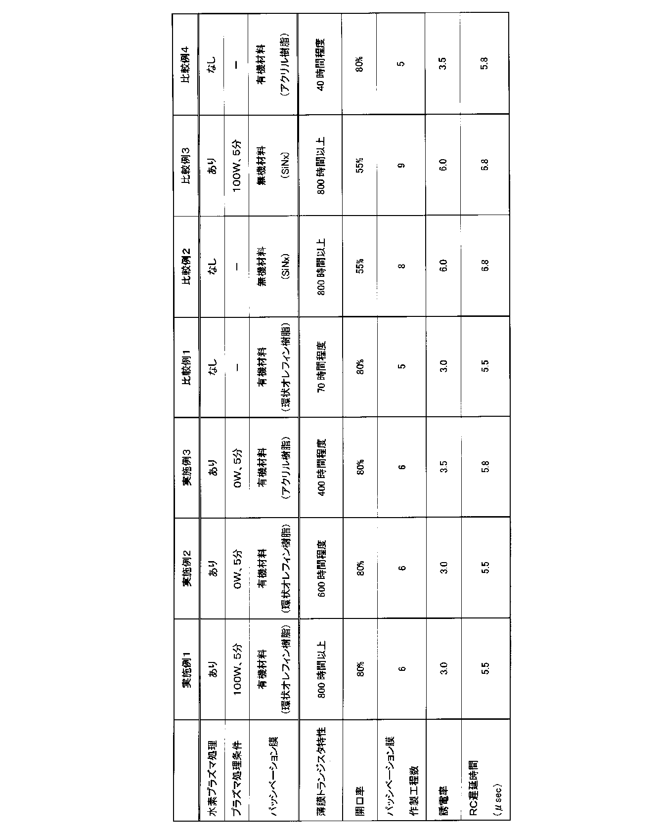
- the off-leakage current value is measured by the above method every 20 hours up to 100 hours and every 100 hours after exceeding 100 hours, and the time when the off-leakage current value reaches 1.0 ⁇ 10 ⁇ 11 A is measured. Observed as thin film transistor characteristics. According to this analysis, the longer the thin film transistor characteristics, the higher the reliability of the thin film transistor.
- the polymerization reaction liquid was obtained by charging and stirring at 80 ° C. for 4 hours while stirring. And the obtained polymerization reaction liquid was put into the autoclave, and it stirred at 150 degreeC and the hydrogen pressure of 4 MPa for 5 hours, and obtained the solution of cyclic olefin resin by performing a hydrogenation reaction.
- the polymerization conversion rate of the cyclic olefin resin in the obtained solution was 99.7%, the weight average molecular weight was 7150, the number average molecular weight was 4690, the molecular weight distribution was 1.52, and the hydrogenation rate was 99.7%.
- the polymerization conversion rate of the acrylic resin in the obtained solution was 99% or more, the weight average molecular weight was 15000, the number average molecular weight was 6500, and the molecular weight distribution was 2.31.
- a solution of the acrylic resin obtained as described above in an amount such that 100 parts of the acrylic resin in the solution is added as a compound having a hydrocarbyloxy group bonded to a silicon atom as 3-glycidoxypropyltriphenyl.
- Example 1 A 200 nm-thick chromium film to be a gate electrode was formed on a glass substrate (Corning, product name Corning 1737) by a sputtering method. Next, in order to pattern the chromium film to form a gate electrode, a positive photoresist (ZPP-1800U3 manufactured by Nippon Zeon Co., Ltd.) used as an etching mask is applied onto the chromium film by a spin coating method, and a hot plate is formed. A 1.5 ⁇ m resist film was formed by removing the solvent. Next, an exposure process and a development process were performed, and the resist film was patterned.
- a positive photoresist ZPP-1800U3 manufactured by Nippon Zeon Co., Ltd.
- the chrome film was patterned by wet etching using diammonium cerium nitrate as an etchant to form a gate electrode.
- a positive photoresist (ZPP-1800U3 manufactured by Nippon Zeon Co., Ltd.) used as an etching mask is applied on the impurity-added semiconductor layer by spin coating. Then, a 1.5 ⁇ m resist film was formed by removing the solvent using a hot plate.
- the resist film was patterned through an exposure process and a development process.
- the impurity-added semiconductor layer and the semiconductor layer were patterned in an island shape by dry etching.
- hydrogen plasma treatment was performed for 5 minutes in a state where a bias of 100 W was applied using a hydrogen plasma treatment apparatus (an apparatus in which Dipole Ring Magnet [manufactured by Tokyo Electron Ltd.] was improved so that plasma treatment was possible).
- the substrate having been subjected to the above steps was rinsed with ultrapure water for 30 seconds, and the ultrapure water adhering at the time of rinsing was removed from the substrate surface using nitrogen.
- the resin composition ( ⁇ ) to be a passivation film containing an organic material is applied onto the substrate that has undergone the above process by a spin coating method, and is heated and dried (prebaked) at 90 ° C. for 2 minutes using a hot plate. Thus, a resin film having a thickness of 2.5 ⁇ m was formed.
- the resin film was irradiated with ultraviolet rays having a light intensity at 365 nm of 5 mW / cm 2 in the air for 40 seconds through a 10 ⁇ m ⁇ 10 ⁇ m hole pattern mask.
- ultraviolet rays having a light intensity at 365 nm of 5 mW / cm 2 in the air for 40 seconds through a 10 ⁇ m ⁇ 10 ⁇ m hole pattern mask.
- Example 2 A thin film transistor was obtained in which a patterned organic passivation film was formed by the same method as in Example 1 except that the bias was set to 0 W in the hydrogen plasma treatment.
- Example 3 A thin film transistor was obtained in which a patterned organic passivation film was formed by the same method as in Example 2 except that the resin composition ( ⁇ ) was used instead of the resin composition ( ⁇ ).
- Example 1 A thin film transistor on which a patterned organic passivation film was formed was prepared and evaluated in the same manner as in Example 1 except that the hydrogen plasma treatment was not performed.
- Example 2 A thin film transistor was fabricated and evaluated in the same manner as in Example 1 except that the passivation film was changed to a silicon nitride film (SiNx film) formed by a CVD method using silane gas and ammonium gas as raw materials.
- SiNx film silicon nitride film
- Comparative Example 3 A thin film transistor was fabricated and evaluated in the same manner as in Comparative Example 2 except that the hydrogen plasma treatment was not performed.
- Comparative Example 4 A thin film transistor on which a patterned organic passivation film was formed was prepared and evaluated in the same manner as in Example 3 except that the hydrogen plasma treatment was not performed. Table 1 also shows the results of evaluating the following characteristics.
- Aperture Ratio The ratio of the area of the portion that allows light to pass except the wiring portion and the transistor portion to the area of the manufactured thin film transistor substrate was determined as the aperture ratio. The higher the aperture ratio, the better the brightness.
- Example 1 that is, in Examples 1 to 3, six steps of (i) hydrogen plasma treatment, (ii) cleaning, (iii) coating, (iv) exposure, (v) development, and (vi) baking are required. In Comparative Examples 1 and 4, five steps of (i) cleaning, (ii) coating, (iii) exposure, (iv) development, and (v) baking are required. In Comparative Example 2, (i) cleaning, (ii) formation of SiNx film by CVD method, (iii) cleaning, (iv) coating, (v) exposure, (vi) development, (vii) baking, ( viii) Eight steps of dry etching are required.
- a silicon nitride film (SiNx film) formed by a CVD method using silane gas and ammonium gas as raw materials is formed on a silicon wafer, and is heated and dried (prebaked) at 90 ° C. for 2 minutes using a hot plate.
- a resin film having a thickness of 120 nm was formed.
- it heated at 230 degreeC for 60 minute (s) and the test sample which consists of a silicon wafer in which the SiNx film
- the relative dielectric constant of the resin film and the SiNx film was measured at 10 kHz (room temperature) according to JIS C6481. The lower the dielectric constant, the better.
- the RC delay was calculated as the RC delay time (DT) by calculating the time required for 97% voltage to reach the end of the data wiring when the input signal was 10 V in 65 inch full high vision.
- V (t) V (1-exp [t / RC])
- V input voltage
- t time
- R resistance of data wiring
- C parasitic capacitance of data wiring
- the thin film transistor using the hydrogen plasma treatment and using the organic material for the passivation film does not deteriorate in a harsh atmosphere and is very reliable.
- the thin film transistor substrate using the passivation film containing an organic material has a smaller number of processes than the one using the passivation film containing SiNx, which is an inorganic material, and can be easily manufactured.
- the passivation film containing an organic material has a high aperture ratio and thus has excellent luminance, and has a low relative dielectric constant, thereby suppressing RC delay.
Landscapes
- Thin Film Transistor (AREA)
- Formation Of Insulating Films (AREA)
- Addition Polymer Or Copolymer, Post-Treatments, Or Chemical Modifications (AREA)
Abstract
Description
(1)半導体素子表面又は前記半導体素子に含まれる半導体層表面に対してプラズマ処理を行う工程と、前記プラズマ処理を行った前記半導体素子表面又は前記半導体層表面に有機材料からなるパッシベーション膜を形成する工程とを含んでなる半導体素子基板の製造方法、
(2)前記プラズマ処理は、水素プラズマ処理であることを特徴とする(1)記載の半導体素子基板の製造方法、
(3)前記半導体素子又は前記半導体層は、基板上に、ゲート電極、ゲート絶縁膜、半導体層及びソース・ドレイン電極を形成する工程と、チャネル領域を形成する工程とを含む工程により製造されることを特徴とする(1)又は(2)に記載の半導体素子基板の製造方法、
(4)前記有機材料は、樹脂を含有する樹脂組成物であることを特徴とする(1)~(3)の何れかに記載の半導体素子基板の製造方法、
(5)前記プラズマ処理は、1~10分の処理時間であることを特徴とする(1)~(4)の何れか一項に記載の半導体素子基板の製造方法、
次いで、図2(a)に示すように、スパッタリング法により、ソース・ドレイン電極26を形成する。次いで、フォトレジスト(図示せず)をマスクとし、エッチングによってソース・ドレイン電極26を図2(b)に示すようにパターニングし、ソース電極27とドレイン電極28を形成する。すなわち、ソース電極27とドレイン電極28は、ソース・ドレイン電極26がパターニングにより分離されて形成されたものであり、ソース・ドレイン電極26とソース電極27とドレイン電極28とは全て同一材料により構成される。一般にソース・ドレイン電極のエッチングはウェットエッチングにより行われるが、ドライエッチングであっても構わない。

これらの樹脂は、それぞれ単独で用いてもよく、又は2種以上を併用してもよい。
一般式(2)において、Xで示される二価の有機基の例としては、メチレン基、エチレン基及びカルボニル基等が挙げられる。
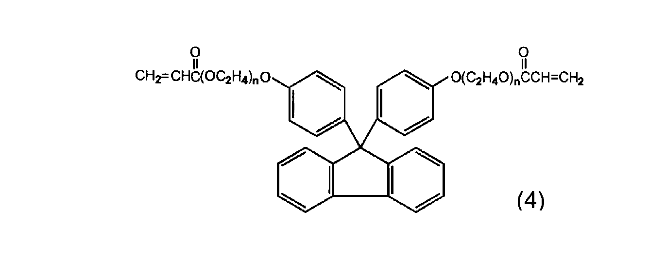
カルド構造を有する単量体は、例えば、ビス(グリシジルオキシフェニル)フルオレン型エポキシ樹脂;ビスフェノールフルオレン型エポキシ樹脂とアクリル酸との縮合物;9,9-ビス(4-ヒドロキシフェニル)フルオレン、9,9-ビス(4-ヒドロキシ-3-メチルフェニル)フルオレン等のカルド構造含有ビスフェノ-ル類;9,9-ビス(シアノメチル)フルオレン等の9,9-ビス(シアノアルキル)フルオレン類;9,9-ビス(3-アミノプロピル)フルオレン等の9,9-ビス(アミノアルキル)フルオレン類;等が挙げられる。カルド樹脂は、カルド構造を有する単量体を重合して得られる重合体であるが、その他の共重合可能な単量体との共重合体であってもよい。上記単量体の重合方法は、常法に従えばよい。
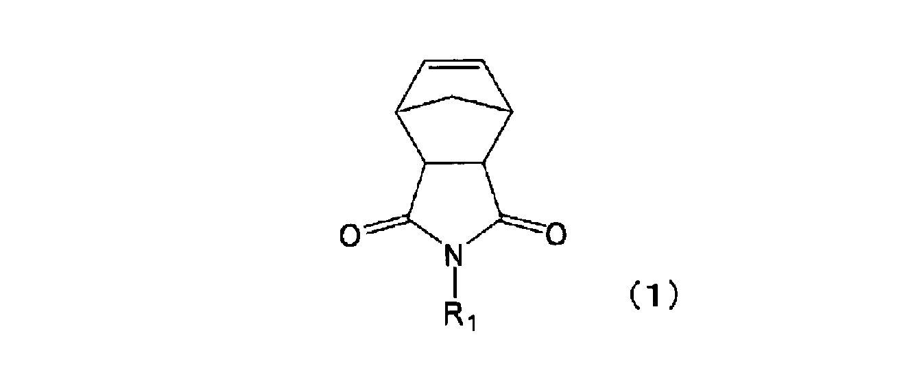
上記一般式(1)において、R1は炭素数5~16の分岐状アルキル基であり、例えば、1-メチルブチル基、2-メチルブチル基、1-メチルペンチル基、1-エチルブチル基、2-メチルヘキシル基、2-エチルヘキシル基、4-メチルヘプチル基、1-メチルノニル基、1-メチルトリデシル基、1-メチルテトラデシル基などが挙げられる。これらの中でも、耐熱性及び有機溶媒への溶解性により優れることから、炭素数6~14の分岐状アルキル基が好ましく、炭素数7~10の分岐状アルキル基がより好ましい。炭素数が4以下であると有機溶媒への溶解性に劣り、炭素数が17以上であると耐熱性に劣り、さらにパターン化された樹脂膜が熱により溶融しパターンを消失してしまうという問題がある。
感放射線化合物(E)としては、例えば、アセトフェノン化合物、トリアリールスルホニウム塩、キノンジアジド化合物等のアジド化合物等が挙げられるが、好ましくはアジド化合物、特に好ましくはキノンジアジド化合物である。
これら以外のフェノール性水酸基を有する化合物としては、2,3,4-トリヒドロキシベンゾフェノン、2,3,4,4’-テトラヒドロキシベンゾフェノン、2-ビス(4-ヒドロキシフェニル)プロパン、トリス(4-ヒドロキシフェニル)メタン、1,1,1-トリス(4-ヒドロキシ-3-メチルフェニル)エタン、1,1,2,2-テトラキス(4-ヒドロキシフェニル)エタン、ノボラック樹脂のオリゴマー、フェノール性水酸基を1つ以上有する化合物とジシクロペンタジエンとを共重合して得られるオリゴマー等が挙げられる。
半導体パラメータアナライザ(Agilent社製4156A)を用いて、作成直後の測定用試料(薄膜トランジスタを有する基板)の、ゲート電圧の変化に対するソースドレイン間電流の変化を測定した。ソース電極とドレイン電極の間に10Vの電圧を印加し、ゲート電圧を-10V~15Vの範囲で0.2V刻みで変化させた時のソースドレイン間電流の最小値をオフリーク電流値として観測した。続いて、測定用試料を温度60℃、湿度90%に設定した恒温恒湿槽(エスペック社製プラチナスPR-2KP)の中に設置した。設置後、100時間までは20時間ごとに、100時間を超えてからは100時間ごとに前記方法によりオフリーク電流値を測定し、オフリーク電流値が1.0×10⁻¹¹Aに達した時間を薄膜トランジスタ特性として観測した。この分析によれば、薄膜トランジスタ特性が長いほど、薄膜トランジスタの信頼性が高くなる。
N-(2-エチルヘキシル)-ビシクロ[2.2.1]ヘプト-5-エン-2,3-ジカルボキシイミド(NEHI)40モル%、及び8-ヒドロキシカルボニルテトラシクロ[4.4.0.12,5.17,10]ドデカ-3-エン(TCDC)60モル%からなる単量体混合物100部、1,5-ヘキサジエン2部、(1,3-ジメチルイミダゾリン-2-イリデン)(トリシクロヘキシルホスフィン)ベンジリデンルテニウムクロリド(Org.Lett.,第1巻,953頁,1999年に記載された方法で合成した)0.02部、及びジエチレングリコールメチルエチルエーテル400部を、窒素置換したガラス製耐圧反応器に仕込み、攪拌しつつ80℃にて4時間反応させて重合反応液を得た。そして、得られた重合反応液をオートクレーブに入れて、150℃、水素圧4MPaで5時間攪拌して水素添加反応を行うことにより、環状オレフィン樹脂の溶液を得た。得られた溶液中の環状オレフィン樹脂の重合転化率は99.7%、重量平均分子量は7150、数平均分子量は4690、分子量分布は1.52、水素添加率は99.7%であった。
次に、以上のようにして得られた環状オレフィン樹脂の溶液(溶液中の環状オレフィン樹脂が100部となる量)に、酸性基を有する化合物として、ピラジン-2,3-ジカルボン酸2部、感放射線化合物として、1,1,3-トリス(2,5-ジメチル-4-ヒドロキシフェニル)-3-フェニルプロパン(1モル)と1,2-ナフトキノンジアジド-5-スルホン酸クロライド(2モル)との縮合物(東洋合成工業社製、「TS200」)30部、架橋剤として、メチルエーテル化メラミン樹脂(サイテックインダストリーズ社製、「サイメル370」)30部、3,4-エポキシシクロヘキセニルメチル-3’,4’-エポキシシクロヘキセンカルボキシレート(ダイセル化学工業社製,「セロキサイド2021P」)30部、及びエポキシ化ブタンテトラカルボン酸テトラキス-(3-シクロヘキセニルメチル)修飾ε-カプロラクトン(ダイセル化学工業社製,「エポリードGT401」)10部、酸化防止剤として、ペンタエリスリトールテトラキス[3-(3,5-ジ-t-ブチル-4-ヒドロキシフェニル)プロピオネート](チバ・スペシャリティーケミカルズ社製、「イルガノックス1010」)1部、並びに界面活性剤として、溶液中の濃度が300ppmとなる量のシリコーン系界面活性剤(信越シリコーン社製、「KP-341」)を添加し、さらにジエチレングリコールメチルエチルエーテル100部を添加して、混合攪拌した。30分攪拌後、この溶液を孔径0.45μmのポリテトラフルオロエチレン製フィルターでろ過して、環状オレフィン樹脂を含み感放射線性を有する樹脂組成物(α)を調製した。
スチレン20部、ブチルメタクリレート25部、2-エチルヘキシルアクリレート25部、メタクリル酸30部、2,2-アゾビスイソブチロニトリル0.5部、及びプロピレングリコールモノメチルエーテルアセテート300部を、窒素置換したガラス製耐圧反応器に仕込み、窒素気流中で攪拌しながら80℃で4時間反応させた。そして、得られた反応溶液をロータリーエバポレーターで濃縮することで、固形分濃度35%でアクリル樹脂の溶液を得た。得られた溶液中のアクリル樹脂の重合転化率は99%以上、重量平均分子量は15000、数平均分子量は6500、分子量分布は2.31であった。
次に、以上のようにして得られたアクリル樹脂の溶液(溶液中のアクリル樹脂が100部となる量)に、ケイ素原子に結合したヒドロカルビルオキシ基を有する化合物として、3-グリシドキシプロピルトリメトキシシラン(東レ・ダウコーニング社製、「SH-6040」)10部、感放射線化合物として、1,1,3-トリス(2,5-ジメチル-4-ヒドロキシフェニル)-3-フェニルプロパン(1モル)と1,2-ナフトキノンジアジド-5-スルホン酸クロライド(2モル)との縮合物(東洋合成工業社製、「TS200」)30部、架橋剤として、メチルエーテル化メラミン樹脂(サイテックインダストリーズ社製、「サイメル350」)50部、酸化防止剤として、ペンタエリスリトールテトラキス[3-(3,5-ジ-t-ブチル-4-ヒドロキシフェニル)プロピオネート](チバ・スペシャリティーケミカルズ社製、「イルガノックス1010」)1部、及び界面活性剤として、溶液中の濃度が300重量ppmとなる量のシリコーン系界面活性剤(信越シリコーン社製、「KP-341」)を添加し、さらにプロピレングリコールモノメチルエーテルアセテート100部を添加して、混合攪拌した。30分攪拌後、この溶液を孔径0.45μmのポリテトラフルオロエチレン製フィルターでろ過して、アクリル樹脂を含み感放射線性を有する樹脂組成物(β)を調製した。
ガラス基板(コーニング社、製品名コーニング1737)上に、ゲート電極となる200nm厚のクロム膜をスパッタリング法により形成した。次いで、前記クロム膜をパターニングしてゲート電極とするため、エッチングのマスクとして使用するポジ型フォトレジスト(日本ゼオン社製ZPP-1800U3)をスピンコート法により前記クロム膜上に塗布し、ホットプレートを用いて溶媒を除去することで1.5μmのレジスト膜を形成した。次いで、露光工程、現像工程を行い、レジスト膜をパターニングした。次いで、硝酸二アンモニウムセリウムをエッチング液に用いて、ウェットエッチングによりクロム膜のパターニングを行いゲート電極を形成した。次いで、レジスト膜を、モノエタノールアミン(MEA)とジメチルスルホキシド(DMSO)の混合溶液(MEA/DMSO=7/3)の剥離液を用いて除去した。
水素プラズマ処理においてバイアスを0Wとした以外は実施例1と同様の方法によりパターン化された有機パッシベーション膜が形成された薄膜トランジスタを得た。
(実施例3)
樹脂組成物(α)に代えて、樹脂組成物(β)を用いた以外は、実施例2と同様の方法によりパターン化された有機パッシベーション膜が形成された薄膜トランジスタを得た。
水素プラズマ処理を行わなかった以外は、実施例1と同様にしてパターン化された有機パッシベーション膜が形成された薄膜トランジスタを作製し、評価を行った。
パッシベーション膜を、シランガスとアンモニウムガスを原料としたCVD法により成膜したシリコン窒化膜(SiNx膜)に変更した以外は、実施例1と同様にして薄膜トランジスタを作製し、評価を行った。
水素プラズマ処理を行わなかった以外は、比較例2と同様にして薄膜トランジスタを作製し、評価を行った。
(比較例4)
水素プラズマ処理を行わなかった以外は、実施例3と同様にしてパターン化された有機パッシベーション膜が形成された薄膜トランジスタを作製し、評価を行った。
また、表1には以下の特性について評価した結果も示した。
作製した薄膜トランジスタ基板の面積に対する配線部及びトランジスタ部を除いた光を通過させる部分の面積の割合を開口率として求めた。開口率が高いほど、輝度に優れている。
図1の(a)~図2(c)に示す工程によって薄膜トランジスタを作製した後にパターン化パッシベーション膜を形成した薄膜トランジスタを得るまでに必要な工程数の比較を行った。
製造例1及び2において作製した有機材料を含んでなる樹脂組成物をシリコンウェハ上にスピンコート法により塗布した後、ホットプレートを用いて90℃で2分間加熱乾燥(プリベーク)して、膜厚2.5μmの樹脂膜を形成した。次いで、230℃で60分間加熱し、有機材料を含む樹脂膜が形成されたシリコンウェハからなる試験用試料を得た。
V(t)=V(1-exp[t/RC])
V:入力電圧、t:時間、R:データ配線の抵抗、C:データ配線の寄生容量
Claims (5)
- 半導体素子表面又は前記半導体素子に含まれる半導体層表面に対してプラズマ処理を行う工程と、
前記プラズマ処理を行った前記半導体素子表面又は前記半導体層表面に有機材料からなるパッシベーション膜を形成する工程と
を含んでなる半導体素子基板の製造方法。 - 前記プラズマ処理は、水素プラズマ処理であることを特徴とする請求項1記載の半導体素子基板の製造方法
- 前記半導体素子又は前記半導体層は、
基板上に、ゲート電極、ゲート絶縁膜、半導体層及びソース・ドレイン電極を形成する工程と、
チャネル領域を形成する工程と
を含む工程により製造されることを特徴とする請求項1又は2記載の半導体素子基板の製造方法。 - 前記有機材料は、樹脂を含有する樹脂組成物であることを特徴とする請求項1~3の何れか一項に記載の半導体素子基板の製造方法。
- 前記プラズマ処理は、1~10分の処理時間であることを特徴とする請求項1~4の何れか一項に記載の半導体素子基板の製造方法。
Priority Applications (3)
| Application Number | Priority Date | Filing Date | Title |
|---|---|---|---|
| JP2012503183A JP5747908B2 (ja) | 2010-03-04 | 2011-03-01 | 半導体素子基板の製造方法 |
| CN201180004752.XA CN102640268B (zh) | 2010-03-04 | 2011-03-01 | 半导体元件基板的制造方法 |
| KR1020127013813A KR101883647B1 (ko) | 2010-03-04 | 2011-03-01 | 반도체 소자 기판의 제조 방법 |
Applications Claiming Priority (2)
| Application Number | Priority Date | Filing Date | Title |
|---|---|---|---|
| JP2010047935 | 2010-03-04 | ||
| JP2010-047935 | 2010-03-04 |
Publications (1)
| Publication Number | Publication Date |
|---|---|
| WO2011108533A1 true WO2011108533A1 (ja) | 2011-09-09 |
Family
ID=44542184
Family Applications (1)
| Application Number | Title | Priority Date | Filing Date |
|---|---|---|---|
| PCT/JP2011/054610 Ceased WO2011108533A1 (ja) | 2010-03-04 | 2011-03-01 | 半導体素子基板の製造方法 |
Country Status (5)
| Country | Link |
|---|---|
| JP (1) | JP5747908B2 (ja) |
| KR (1) | KR101883647B1 (ja) |
| CN (1) | CN102640268B (ja) |
| TW (1) | TWI509704B (ja) |
| WO (1) | WO2011108533A1 (ja) |
Cited By (8)
| Publication number | Priority date | Publication date | Assignee | Title |
|---|---|---|---|---|
| JP2013219173A (ja) * | 2012-04-09 | 2013-10-24 | Jsr Corp | 半導体素子、半導体基板、感放射線性樹脂組成物、保護膜および表示素子 |
| WO2015080071A1 (ja) * | 2013-11-28 | 2015-06-04 | 国立大学法人東北大学 | 半導体素子の製造方法 |
| US9082981B1 (en) | 2012-01-16 | 2015-07-14 | Polyera Corporation | Curable polymeric materials and related electronic devices |
| JP2015228527A (ja) * | 2012-01-23 | 2015-12-17 | 日立化成株式会社 | 半導体基板用パッシベーション膜形成用材料、半導体基板用パッシベーション膜を有する半導体基板の製造方法、太陽電池素子及び太陽電池素子の製造方法 |
| US9437830B2 (en) | 2013-08-12 | 2016-09-06 | Samsung Display Co., Ltd. | Display device |
| JP2018082211A (ja) * | 2012-01-06 | 2018-05-24 | 日立化成株式会社 | パッシベーション膜形成用組成物、パッシベーション膜付半導体基板及びその製造方法、並びに太陽電池素子及びその製造方法 |
| US10147895B2 (en) | 2015-07-13 | 2018-12-04 | Flexterra, Inc. | Curable polymeric materials and their use for fabricating electronic devices |
| US11345778B2 (en) | 2018-01-19 | 2022-05-31 | Flexterra, Inc. | Organic dielectric materials and devices including them |
Families Citing this family (3)
| Publication number | Priority date | Publication date | Assignee | Title |
|---|---|---|---|---|
| WO2014027618A1 (ja) * | 2012-08-13 | 2014-02-20 | 日本ゼオン株式会社 | 薄膜トランジスタ |
| US8907385B2 (en) * | 2012-12-27 | 2014-12-09 | Taiwan Semiconductor Manufacturing Company, Ltd. | Surface treatment for BSI image sensors |
| KR20170087568A (ko) | 2016-01-20 | 2017-07-31 | 삼성디스플레이 주식회사 | 액정 표시 장치 및 이의 제조 방법 |
Citations (2)
| Publication number | Priority date | Publication date | Assignee | Title |
|---|---|---|---|---|
| JP2000214481A (ja) * | 1999-01-22 | 2000-08-04 | Advanced Display Inc | 液晶表示装置およびその製造方法 |
| JP2002368229A (ja) * | 2001-04-04 | 2002-12-20 | Canon Inc | 半導体装置、及びその製造方法、並びに放射線検出装置 |
Family Cites Families (8)
| Publication number | Priority date | Publication date | Assignee | Title |
|---|---|---|---|---|
| JP2000260299A (ja) * | 1999-03-09 | 2000-09-22 | Matsushita Electric Ind Co Ltd | 冷電子放出素子及びその製造方法 |
| US6794682B2 (en) * | 2001-04-04 | 2004-09-21 | Canon Kabushiki Kaisha | Semiconductor device, method for manufacturing the same, and radiation detector |
| JP2003037269A (ja) | 2001-07-25 | 2003-02-07 | Nec Kagoshima Ltd | 薄膜トランジスタの製造方法 |
| JP4904671B2 (ja) * | 2004-06-24 | 2012-03-28 | 日本電気株式会社 | 半導体装置、その製造方法及び電子機器 |
| KR100683777B1 (ko) * | 2005-05-24 | 2007-02-20 | 삼성에스디아이 주식회사 | 유기박막 트랜지스터 및 그의 제조방법과 유기 박막트랜지스터를 구비한 평판표시장치 |
| KR20070059234A (ko) * | 2005-12-06 | 2007-06-12 | 삼성전자주식회사 | 암전류를 감소시키기 위한 이미지 센서의 제조 방법 |
| US8692251B2 (en) | 2007-11-02 | 2014-04-08 | Sharp Kabushiki Kaisha | Circuit board and display device |
| WO2009131035A1 (ja) * | 2008-04-25 | 2009-10-29 | 株式会社アルバック | 薄膜トランジスタの製造方法、薄膜トランジスタ |
-
2011
- 2011-03-01 WO PCT/JP2011/054610 patent/WO2011108533A1/ja not_active Ceased
- 2011-03-01 KR KR1020127013813A patent/KR101883647B1/ko not_active Expired - Fee Related
- 2011-03-01 CN CN201180004752.XA patent/CN102640268B/zh not_active Expired - Fee Related
- 2011-03-01 JP JP2012503183A patent/JP5747908B2/ja not_active Expired - Fee Related
- 2011-03-02 TW TW100106840A patent/TWI509704B/zh active
Patent Citations (2)
| Publication number | Priority date | Publication date | Assignee | Title |
|---|---|---|---|---|
| JP2000214481A (ja) * | 1999-01-22 | 2000-08-04 | Advanced Display Inc | 液晶表示装置およびその製造方法 |
| JP2002368229A (ja) * | 2001-04-04 | 2002-12-20 | Canon Inc | 半導体装置、及びその製造方法、並びに放射線検出装置 |
Cited By (20)
| Publication number | Priority date | Publication date | Assignee | Title |
|---|---|---|---|---|
| JP2018082211A (ja) * | 2012-01-06 | 2018-05-24 | 日立化成株式会社 | パッシベーション膜形成用組成物、パッシベーション膜付半導体基板及びその製造方法、並びに太陽電池素子及びその製造方法 |
| US9929345B1 (en) | 2012-01-16 | 2018-03-27 | Flexterra, Inc. | Curable polymeric materials and their use for fabricating electronic devices |
| US9431234B1 (en) | 2012-01-16 | 2016-08-30 | Polyera Corporation | Curable polymeric materials and their use for fabricating electronic devices |
| US9082981B1 (en) | 2012-01-16 | 2015-07-14 | Polyera Corporation | Curable polymeric materials and related electronic devices |
| JP2015228527A (ja) * | 2012-01-23 | 2015-12-17 | 日立化成株式会社 | 半導体基板用パッシベーション膜形成用材料、半導体基板用パッシベーション膜を有する半導体基板の製造方法、太陽電池素子及び太陽電池素子の製造方法 |
| JP2013219173A (ja) * | 2012-04-09 | 2013-10-24 | Jsr Corp | 半導体素子、半導体基板、感放射線性樹脂組成物、保護膜および表示素子 |
| US10497886B2 (en) | 2013-08-12 | 2019-12-03 | Samsung Display Co., Ltd. | Display device |
| US9437830B2 (en) | 2013-08-12 | 2016-09-06 | Samsung Display Co., Ltd. | Display device |
| US11991919B2 (en) | 2013-08-12 | 2024-05-21 | Samsung Display Co., Ltd. | Display device |
| US11600794B2 (en) | 2013-08-12 | 2023-03-07 | Samsung Display Co., Ltd. | Display device |
| US9722195B2 (en) | 2013-08-12 | 2017-08-01 | Samsung Display Co., Ltd. | Display device |
| US10998513B2 (en) | 2013-08-12 | 2021-05-04 | Samsung Display Co., Ltd. | Display device |
| WO2015080071A1 (ja) * | 2013-11-28 | 2015-06-04 | 国立大学法人東北大学 | 半導体素子の製造方法 |
| CN105993065B (zh) * | 2013-11-28 | 2019-03-08 | 国立大学法人东北大学 | 半导体元件的制造方法 |
| US10446690B2 (en) | 2013-11-28 | 2019-10-15 | Tohoku University | Method of production of semiconductor device |
| KR20160093610A (ko) | 2013-11-28 | 2016-08-08 | 고쿠리츠다이가쿠호진 도호쿠다이가쿠 | 반도체 소자의 제조 방법 |
| JPWO2015080071A1 (ja) * | 2013-11-28 | 2017-03-16 | 国立大学法人東北大学 | 半導体素子の製造方法 |
| CN105993065A (zh) * | 2013-11-28 | 2016-10-05 | 国立大学法人东北大学 | 半导体元件的制造方法 |
| US10147895B2 (en) | 2015-07-13 | 2018-12-04 | Flexterra, Inc. | Curable polymeric materials and their use for fabricating electronic devices |
| US11345778B2 (en) | 2018-01-19 | 2022-05-31 | Flexterra, Inc. | Organic dielectric materials and devices including them |
Also Published As
| Publication number | Publication date |
|---|---|
| KR101883647B1 (ko) | 2018-07-31 |
| TWI509704B (zh) | 2015-11-21 |
| JPWO2011108533A1 (ja) | 2013-06-27 |
| KR20130029040A (ko) | 2013-03-21 |
| JP5747908B2 (ja) | 2015-07-15 |
| CN102640268B (zh) | 2016-03-23 |
| TW201145399A (en) | 2011-12-16 |
| CN102640268A (zh) | 2012-08-15 |
Similar Documents
| Publication | Publication Date | Title |
|---|---|---|
| JP5747908B2 (ja) | 半導体素子基板の製造方法 | |
| JP5488460B2 (ja) | 感放射線樹脂組成物、積層体及びその製造方法ならびに半導体デバイス | |
| WO2012165448A1 (ja) | 樹脂組成物および半導体素子基板 | |
| JP6947027B2 (ja) | 樹脂組成物、樹脂膜、及び電子部品 | |
| JP6601394B2 (ja) | 感放射線性樹脂組成物、樹脂膜、および電子部品 | |
| JPWO2012133617A1 (ja) | 樹脂組成物および半導体素子基板 | |
| JP5589286B2 (ja) | 薄膜トランジスタの製造方法、及び薄膜トランジスタ並びに表示装置 | |
| JP6509740B2 (ja) | 半導体素子の製造方法 | |
| JP6248561B2 (ja) | 感放射線性樹脂組成物、及び積層体 | |
| JP2013130816A (ja) | 永久膜用樹脂組成物及び電子部品 | |
| JP5682413B2 (ja) | 半導体素子基板 | |
| JP2012049300A (ja) | 半導体素子基板 | |
| JP5664173B2 (ja) | 半導体素子基板 | |
| JP2012171993A (ja) | 樹脂組成物および半導体素子基板 | |
| JP6079277B2 (ja) | 感放射線樹脂組成物及び電子部品 | |
| JP2012171994A (ja) | 樹脂組成物および半導体素子基板 |
Legal Events
| Date | Code | Title | Description |
|---|---|---|---|
| WWE | Wipo information: entry into national phase |
Ref document number: 201180004752.X Country of ref document: CN |
|
| 121 | Ep: the epo has been informed by wipo that ep was designated in this application |
Ref document number: 11750643 Country of ref document: EP Kind code of ref document: A1 |
|
| WWE | Wipo information: entry into national phase |
Ref document number: 2012503183 Country of ref document: JP |
|
| ENP | Entry into the national phase |
Ref document number: 20127013813 Country of ref document: KR Kind code of ref document: A |
|
| NENP | Non-entry into the national phase |
Ref country code: DE |
|
| 122 | Ep: pct application non-entry in european phase |
Ref document number: 11750643 Country of ref document: EP Kind code of ref document: A1 |