WO2011108430A1 - レンズ駆動装置およびカメラモジュール - Google Patents
レンズ駆動装置およびカメラモジュール Download PDFInfo
- Publication number
- WO2011108430A1 WO2011108430A1 PCT/JP2011/054093 JP2011054093W WO2011108430A1 WO 2011108430 A1 WO2011108430 A1 WO 2011108430A1 JP 2011054093 W JP2011054093 W JP 2011054093W WO 2011108430 A1 WO2011108430 A1 WO 2011108430A1
- Authority
- WO
- WIPO (PCT)
- Prior art keywords
- base
- coil
- driving device
- lens driving
- lens
- Prior art date
- Legal status (The legal status is an assumption and is not a legal conclusion. Google has not performed a legal analysis and makes no representation as to the accuracy of the status listed.)
- Ceased
Links
Images


Classifications
-
- G—PHYSICS
- G02—OPTICS
- G02B—OPTICAL ELEMENTS, SYSTEMS OR APPARATUS
- G02B7/00—Mountings, adjusting means, or light-tight connections, for optical elements
- G02B7/02—Mountings, adjusting means, or light-tight connections, for optical elements for lenses
- G02B7/04—Mountings, adjusting means, or light-tight connections, for optical elements for lenses with mechanism for focusing or varying magnification
- G02B7/08—Mountings, adjusting means, or light-tight connections, for optical elements for lenses with mechanism for focusing or varying magnification adapted to co-operate with a remote control mechanism
-
- H—ELECTRICITY
- H04—ELECTRIC COMMUNICATION TECHNIQUE
- H04N—PICTORIAL COMMUNICATION, e.g. TELEVISION
- H04N23/00—Cameras or camera modules comprising electronic image sensors; Control thereof
- H04N23/57—Mechanical or electrical details of cameras or camera modules specially adapted for being embedded in other devices
Definitions
- the present invention relates to a lens driving device and a camera module including the same.
- Such a camera module includes a lens driving device for focus adjustment.
- the lens driving device displaces the lens in the optical axis direction according to the control signal. Thereby, the focus adjustment with respect to the subject is performed.
- a moving magnet type lens driving device As a lens driving device, a moving magnet type lens driving device is known (for example, Patent Document 1).
- a magnet is attached to a holder that holds a lens.
- the holder is supported so as to be displaceable in the optical axis direction of the lens with respect to the base.
- a coil is arranged on the base so as to face the magnet on the holder side.
- the holder is driven along with the magnet in the optical axis direction of the lens by an electromagnetic driving force generated by applying a current to the coil.
- an image sensor for receiving light collected by the lens is disposed under the base.
- the image sensor is mounted on a predetermined circuit board, and a lens driving device is disposed thereon.
- a terminal for applying a current to the coil is disposed on the base. Both ends of the coil are connected to two terminals, and a signal line is connected to these terminals from the main body side circuit unit. At this time, if the terminal protrudes from the bottom of the base, it is necessary to provide an interval corresponding to the protruding amount of the terminal between the circuit board disposed below the base and the base. Due to this distance, the dimension from the circuit board to the upper surface of the lens driving device becomes large, causing a problem that the outer shape of the camera module becomes large.
- the present invention has been made to solve such a problem, and provides a lens driving device capable of making the outer shape of a camera module compact by devising the arrangement of coil terminals, and a camera module using the lens driving device. For the purpose.
- a lens driving device includes a base, a holder that holds the lens and is supported so as to be displaceable in the optical axis direction of the lens with respect to the base, a magnet mounted on the holder, and a magnet A coil mounted on the base so as to face each other; and a terminal board electrically connected to the coil and provided with a terminal portion for applying a current to the coil.
- a concave portion is formed in the side surface of the base, and the terminal board is mounted in the concave portion so that the lower end does not protrude from the lower surface of the base.
- the second aspect of the present invention relates to a camera module.
- a camera module according to this aspect applies a control signal to the lens driving device according to the above aspect, an image sensor that receives light collected by the lens, a circuit board on which the image sensor is mounted, and the coil. And a control unit.
- a housing portion having a depth for housing the image sensor is formed on the lower surface of the base.
- the recess is formed at a position corresponding to the housing portion on the side surface of the base, and the coil is wound around the optical axis of the lens on the side surface of the base above the recess.
- the lens driving device is installed on the circuit board so that the imaging element is accommodated in the accommodating portion of the base.
- the shape of the camera module in the optical axis direction of the lens can be reduced, and the outer shape of the camera module can be made compact.
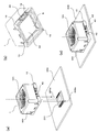
- FIG. 1 is a diagram showing a configuration of a lens driving device.
- FIG. 1A is an exploded perspective view of the lens driving device.
- FIG. 1B is a perspective view showing the configuration of the lens driving device before the cover 100 is attached, and
- FIG. 1C is a perspective view of the lens driving device with the cover 100 attached. .
- the lens is not shown for convenience.
- the lens driving device includes a base 10, a coil 20, magnetic plates 31 and 32 (the magnetic plate 32 is not shown in FIG. 1), a printed circuit board 40, a filter 50, and a holder 60.
- the base 10 has a square shape with chamfered corners in plan view.
- a series of coils 20 are attached to the base 10 in two stages. The winding direction of the coils 20 at each stage is opposite to each other. Magnetic plates 31 and 32 are bonded to the outer surface of the coil 20.
- a printed circuit board 40 is attached to the side surface of the base 10, and two ends of the coil 20 are soldered to the printed circuit board 40. Further, a step (not shown) is formed on the back surface of the base 10, and the filter 50 is attached to the step.
- the filter 50 is an infrared ray removal filter.
- the holder 60 has an octagonal shape in plan view.
- a circular opening 61 for accommodating the lens barrel is formed in the holder 60 at the center position.
- the optical axis of the lens coincides with the center of the octagon defined by the outer shape of the holder 60 in plan view.
- the eight side surfaces of the holder 10 are arranged so as to be symmetric with respect to the optical axis of the lens mounted in the opening 61. Of these eight side surfaces, magnets 70 are mounted on four side surfaces that are not adjacent to each other.
- the four magnets 70 are, for example, sintered magnets made of neodymium or the like, and have a two-pole arrangement structure in which N and S are magnetized on one side. The size and magnetic strength of each magnet 70 are equal to each other. Further, each magnet 70 is arranged at a position where the center thereof is shifted upward by a certain distance from the center of the corresponding side surface. The two magnets 70 are arranged symmetrically with respect to the optical axis of the lens, and the remaining two magnets 70 are also arranged symmetrically with respect to the optical axis of the lens.
- the holder 60 is formed with holes 62 and kerfs 63 at diagonal positions.
- a shaft 90 is passed through the hole 62 and the cut groove 63, and the holder 60 is supported so as to be displaceable in the optical axis direction of the lens.
- the shaft 90 is made of a metal member and has a circular cross section.
- the cover 100 has a square shape with chamfered corners in plan view.
- the outer shape of the cover 100 in plan view is substantially equal to the outer shape of the base 10.
- the shape of the inner surface of the cover 100 in plan view is substantially the same as the outer shape of the portion of the base 10 where the coil 20 and the magnetic plates 31 and 32 are mounted.
- the cover 100 is formed with an opening 101 through which light passes.
- a collar portion 102 and a hole 102a are formed on the side surface of the cover 100, and foot portions 103 are formed at four corners, respectively.
- FIG. 2A is a perspective view showing the configuration of the base 10
- FIG. 2B is a perspective view when the base 10 is viewed from above
- FIG. 2C is the vicinity of the locking piece 16b of the base 10. It is the figure which looked at the part from the upper side.
- the base 10 is made of a frame-shaped member.
- the base 10 is formed with an opening 11 for allowing light to pass through.
- coil mounting portions 12 a and 12 b for winding the coil 20 are formed on the side surface of the base 10 over the entire circumference.
- a shaft holding portion 13 is formed on the upper surface of the base 10, and a hole 13 a for press-fitting the shaft 90 is formed in the shaft holding portion 13.
- a hole 13b for press-fitting the shaft 90 is formed at a position coaxial with the hole 13a.
- a receiving portion 14 to which the shaft holder 80 is attached is formed on the upper surface of the base 10 at a position that is diagonally related to the shaft holding portion 13.
- the receiving portion 14 is formed with a hole portion 14a that fits with the protrusion 83 (see FIG. 3A) of the shaft holder 80. Further, in the vicinity of the receiving portion 14, a notch 14 b that engages with the flange portion 81 of the shaft holder 80 is formed. Further, a hole 14 c into which the shaft 90 is press-fitted is formed below the receiving portion 14. When the shaft holder 80 is attached to the receiving portion 14, the hole 14c faces the hole 82 (see FIG. 3A) of the shaft holder 80.
- a step portion 15 is formed on the side surface of the base 10, and a locking piece 15 a is formed on the step portion 15. Further, a recess 16 is formed on the other side surface of the base 10, and two protrusions 16 a are formed in the recess 16. Two locking pieces 16 b are formed above the recess 16. As shown in FIG. 5C, each of the two locking pieces 16b has an inclined surface on the right side. When the coil 20 is mounted on the printed circuit board 40, the intermediate portion of the coil 20 is locked to the inclined surface.
- the printed circuit board 40 has two holes 41 at positions corresponding to the two protrusions 16a. Further, the terminal portion 42 is exposed to the outside from around the hole 41 to the lower end. The protrusions 16 a are inserted into the two holes 41 and the printed circuit board 40 is mounted in the recess 16. Details of the mounting method of the printed circuit board 40 will be described later with reference to FIG.
- a groove 17 is formed in the base 10 above the step portion 15.
- the groove 17 functions as an adhesive reservoir groove when the magnetic plate 31 is bonded to the outer surface of the coil 20 as will be described later.
- Grooves 18 functioning as an adhesive reservoir groove when another magnetic plate 32 is bonded are also formed on the other side surface (see FIG. 4B).
- stepped portions 10 a that contact the foot portions 103 of the cover 100 are formed at the four corners of the lower portion of the base 10.
- the printed circuit board 40 is mounted in the recess 16 of the base 10 shown in FIG. Further, the coil 20 is mounted and the end of the coil 20 is soldered to the printed circuit board 40. Thereafter, the holder 60 to which the lens and the magnet 70 are attached is accommodated in the frame of the base 10 from above the base 10.
- FIG. 3A is a diagram illustrating a state in which the holder 60 is accommodated in the base 10. As shown in the figure, the two end portions 20a and 20b of the coil 20 reach the printed circuit board 40 via the locking pieces 16b. The arrows in the figure indicate the winding direction of the coil 20.
- FIG. 3 (c) is a diagram showing a state in which the end portions 20a and 20b of the coil 20 are mounted.
- the end 20a of the coil 20 is wound around the left protrusion 16a.
- the end 20a is hung on the inclined surface of the left locking piece 16b shown in FIG. 2A (see FIG. 2C), and clockwise (see FIG. 2C) on the coil mounting portion 12b on the lower side of the base 10. It is wound in the direction of the arrow on the lower side of FIG.
- the coil 20 is wound around the upper coil mounting portion 12a in the counterclockwise direction (the arrow direction on the upper side in FIG. 3A).
- the end 20b of the coil 20 is hung on the inclined surface of the right locking piece 16a (see FIG. 2 (c)), as shown in FIG. 3 (c). And wound around the right protrusion 16a. Thereafter, soldering is performed so as to connect the end portions 20a and 20b wound around the protrusion 16a and the terminal portion 42 corresponding to each end portion. Thus, the coil 20 and the terminal portion 42 are electrically connected.
- the printed circuit board 40 is fastened so as not to come out of the recess 16 by soldering. In this state, the printed circuit board 40 and the recess 16 may be bonded and fixed.
- the shaft holder 80 is attached to the receiving portion 14 so that the protrusion 83 is fitted into the hole 14a on the base side (see FIG. 2B).
- the flange portion 81 of the shaft holder 80 is engaged with the notch 14 b on the upper surface of the base 10.
- FIG. 3B is a view showing a state in which the shaft holder 80 is thus attached to the receiving portion 14.
- the holes 13a and 13b and the hole 62 of the holder 60 are aligned, and one shaft 90 is press-fitted from the hole 13a.
- the tip of the shaft 90 is press-fitted into the hole 13a, passes through the hole 62, and is then press-fitted into the hole 13b (see FIG. 2A).
- the rear end of the shaft 90 is supported by the hole 13a.
- the hole 82 of the shaft holder 80, the hole 14c of the base 10 (see FIG. 2B), and the kerf 63 of the holder 60 (see FIG. 1A) are aligned, and the other The shaft 90 is press-fitted from the hole 82.
- the tip of the shaft 90 is press-fitted into the hole 82, passes through the kerf 63, and is then press-fitted into the hole 13c.
- the rear end of the shaft 90 is supported by the hole 82.
- the holder 60 is attached to the base 10 so as to be displaceable in the optical axis direction of the lens. Thereafter, the two magnetic plates 31 and 32 are bonded to the outer surface of the coil 20.
- FIG. 4 (a) and 4 (b) are diagrams showing the mounting state of the magnetic plates 31 and 32.
- FIG. 1A is a perspective view when the lens driving device is viewed from substantially the same angle as FIG. 1B
- FIG. 1B is a perspective view of the lens driving device from the state of FIG. It is a perspective view of the state rotated about 90 degrees in the counterclockwise direction about the axis.
- a magnetic plate 32 is bonded to the outer surface of the coil 20 in addition to the magnetic plate 31.
- the magnetic plate is not attached to the other side surface other than the two side surfaces in FIG.
- a groove 18 is formed in the vicinity of the magnetic plate 32 of the base 10. At the time of bonding of the magnetic plates 31 and 32, the grooves 17 and 18 function as an adhesive reservoir groove.
- the cover 100 is mounted on the base from above as shown in FIG.
- the flange portion 102 of the cover is fitted into the step portion 15 of the base 10, and the hole 102 a of the flange portion 102 is engaged with the locking piece 15 a of the step portion 15.
- the foot portion 103 of the cover 100 abuts on the upper surface of the step portion 10 a of the base 10. In this way, the assembly of the lens driving device is completed as shown in FIG. In such an assembled state, the terminal portion 42 of the printed circuit board 40 is exposed to the outside without being covered by the cover 100.
- FIG. 5 is a diagram for explaining the driving operation of the lens driving device. This figure schematically shows the A-A 'cross section of FIG.
- a black dot mark on the circle and a cross mark on the circle indicate the direction of current flow.
- a black dot mark on the circle indicates a direction toward the drawing reference person, and a cross mark on the circle indicates a direction away from the drawing reference person.
- the N-pole region of the magnet 70 is opposed to the upper portion 21 of the coil 20, and the S-pole region of the magnet 70 is opposed to the lower portion 22.
- a current in the direction shown in FIG. 5A flows through the coil 20
- an upward driving force acts on the magnet 70
- the lens holder 60 is displaced upward in the figure.
- the lens holder 60 is displaced upward as shown in FIG.
- the holder 60 is pressed against the shaft 90 by the magnetic force between the magnetic plates 31 and 32 and the magnet 70 and is held at the position when the current application is stopped.
- 7B when a reverse current is applied to the coil 20, the lens holder 60 is displaced downward.
- the lens is positioned at the on-focus position by moving the lens holder 60 upward and downward.
- the home position of the lens holder 60 is a position where the lower surface of the lens holder 60 comes into contact with the base 10.
- FIG. 6 is a diagram showing a schematic configuration of a camera module on which the lens driving device having the above configuration is mounted.
- reference numeral 1 denotes a lens driving device.
- the base 10 is provided with a hall element 110 as a position sensor, and the position of the lens holder 60 is detected based on a signal from the hall element 110.
- a CPU (Central Processing Unit) 301 controls the driver 302 to displace the lens holder 60 from the home position to a predetermined position in the lens optical axis direction.
- a position detection signal from the Hall element 110 is input to the CPU 301.
- the CPU 301 processes a signal input from the image sensor 201 to acquire a contrast value of the captured image. Then, the position of the lens holder 60 with the best contrast value is acquired as the on-focus position.
- the CPU 301 drives the lens holder 60 toward the acquired on-focus position.
- the CPU 301 monitors the signal from the hall element 110 and drives the lens holder 60 until the signal from the hall element 110 reaches a state corresponding to the on-focus position. Thereby, the lens holder 60 is positioned at the on-focus position.
- FIG. 7 is a diagram for explaining a method of mounting the lens driving device 1 on the circuit board 200.
- FIG. 4A is a perspective view showing a state before the lens driving device 1 is mounted on the circuit board 200
- FIG. 4B is a perspective view of the lens driving device 1 viewed from the back side
- FIG. FIG. 6 is a perspective view showing a state after the lens driving device 1 is mounted on the circuit board 200.
- two pins 19 are formed on the lower surface of the base 10 at diagonal positions.
- an accommodation portion S having a depth capable of accommodating the image sensor 201 in a state where the filter 50 is mounted is provided on the lower surface of the base.
- the concave portion 16 is formed at a position corresponding to the accommodating portion on the side surface of the base.
- a hole 200a is formed in the circuit board 200 at a position corresponding to the pin 19 of the base 10.
- the lens driving device 1 is installed on the circuit board 200 from above as shown in FIG. At this time, the two pins 19 of the base 10 are fitted into the two holes 200 a of the circuit board 200. Thereby, the lens driving device 1 is correctly positioned with respect to the image sensor 201. In this state, the lens driving device 1 is bonded and fixed to the circuit board 200. As a result, the lens driving device 1 is installed on the circuit board 200 as shown in FIG.
- the lower end of the printed circuit board 40 does not protrude from the lower surface of the base 10, there is no need to leave a gap between the base 10 and the circuit board 200. Therefore, the shape of the camera module in the optical axis direction of the lens can be reduced, and the outer shape of the camera module can be made compact.
- the lens driving device 1 since the lens driving device 1 is mounted on the upper surface of the circuit board 200 so that the image sensor 201 is accommodated in the accommodating portion S of the base 10, the camera module in the optical axis direction of the lens. The shape of the camera module can be further reduced, and the outer shape of the camera module can be made more compass. In addition, since the image sensor 201 is covered by the lens driving device 1, the image sensor 201 can be protected by the lens driving device 1.
- the end portions 20a and 20b of the coil 20 are wound around the protrusion 16a, so that the end of the coil 20 can be easily handled while the coil 20 is being cleaned.
- the portions 20 a and 20 b can be positioned at the position of the terminal portion 42 of the printed circuit board 40. Further, by soldering the position of the protrusion 16a, the end portions 20a and 20b of the coil 20 can be easily connected to the corresponding terminal portions 42.
- the terminal portion 42 is exposed to the outside without being covered with the cover 100, and therefore, the signal line can be easily attached to the terminal portion 42. be able to.
- the signal line is attached to the terminal portion 42 by soldering.
- the signal line may be performed in the state of FIG. 7C or may be performed before the lens driving device 1 is mounted on the circuit board 200.
- the terminal portion 42 is exposed to the outside by not covering the lower portion of the base 10 with the cover 100.
- the lower part may be covered with the cover 100, and a notch may be provided at a position corresponding to the terminal part 42 of the cover 100 to expose the terminal part 42 to the outside.
- Fig.3 (a) although the intermediate part of the edge parts 20a and 20b of the coil 20 was relayed to the locking piece 16b, although two locking pieces 16b are used. Either or both may be omitted, and the coils 20a and 20b may be directly wound around the corresponding protrusion 16a.
- the coil 20 is wound around the coil mounting portions 12a and 12b of the base 10 before being wound around the two protrusions 16a, and then the printed circuit board 20 is mounted in the recess 16 and the coil end portions 20a and 20b are wound around the protrusion 16a. It can also be done.
- an inclined surface is formed on the left side of the left locking piece 16b shown in FIG. 2C, and an end 20a of the coil 20 is hung on the inclined surface and is wound around the left protrusion 16a.
- one magnet 70 is disposed on one side surface of the holder 60, but two or more magnets may be disposed on each side surface.
- the two magnetic plates 31 and 32 are arranged on the base 10, but one or three or more magnetic plates may be arranged on the base 10.
- the shapes of the base 10 and the holder 60 are not limited to the above, and can be changed as appropriate.
- the diameters of the two shafts 90 may not be the same, and the holder 60 may be guided in the optical axis direction of the lens by a guide mechanism other than the shafts.
Landscapes
- Physics & Mathematics (AREA)
- General Physics & Mathematics (AREA)
- Optics & Photonics (AREA)
- Engineering & Computer Science (AREA)
- Multimedia (AREA)
- Signal Processing (AREA)
- Lens Barrels (AREA)
- Studio Devices (AREA)
Abstract
【課題】コイル用端子の配置を工夫することにより、カメラモジュールの外形をコンパクトにできるレンズ駆動装置およびこれを用いたカメラモジュールを提供する。 【解決手段】 ベース10の側面に凹部16が形成され、この凹部16に突起16aが形成されている。プリント基板40は、孔41が突起16aに挿入されるようにして、凹部16に嵌め込まれる。この状態で、コイル20の端部20a、20bが、それぞれ、対応する突起16aに巻き付けられる。その後、コイル20の端部20a、20bと端子部42とを繋ぐように半田付けが行われ、端部20a、20bと端子部42とが接続される。
Description
本発明は、レンズ駆動装置およびこれを備えたカメラモジュールに関する。
従来、携帯電話機等にはカメラモジュールが搭載されている。かかるカメラモジュールは、フォーカス調節のためにレンズ駆動装置を備えている。レンズ駆動装置は、制御信号に応じてレンズを光軸方向に変位させる。これにより、被写体に対するフォーカス調節が行われる。
レンズ駆動装置の一つとして、ムービングマグネット方式のレンズ駆動装置が知られている(たとえば、特許文献1)。この種のレンズ駆動装置では、レンズを保持するホルダに、磁石が装着される。ホルダは、ベースに対し、レンズの光軸方向に変位可能に支持される。ベースには、ホルダ側の磁石に向き合うようにコイルが配置される。コイルに電流を印加することにより生じる電磁駆動力によって、ホルダが磁石とともに、レンズの光軸方向に駆動される。
かかるレンズ駆動装置がカメラモジュールに搭載される場合、ベースの下には、レンズによって集光された光を受光するためのイメージセンサが配置される。イメージセンサは、所定の回路基板に装着され、この上に、レンズ駆動装置が配置される。
上記レンズ駆動装置において、ベースには、コイルに電流を印加するための端子が配置される。コイルの両端が2つの端子に接続され、この端子に、本体側回路部から信号線が接続される。このとき、端子がベースの下から突出していると、ベースの下に配置される上記回路基板とベースとの間に、端子の突出量に応じた間隔を空ける必要がある。この間隔のために、回路基板からレンズ駆動装置の上面までの寸法が大きくなり、カメラモジュールの外形が大きくなるとの問題が生じる。
本発明は、かかる課題を解消するために為されたものであり、コイル用端子の配置を工夫することにより、カメラモジュールの外形をコンパクトにできるレンズ駆動装置およびこれを用いたカメラモジュールを提供することを目的とする。
本発明の第1の態様は、レンズ駆動装置に関する。この態様に係るレンズ駆動装置は、ベースと、レンズを保持するとともに前記ベースに対して前記レンズの光軸方向に変位可能に支持されたホルダと、前記ホルダに装着された磁石と、前記磁石に向き合うように前記ベースに装着されたコイルと、前記コイルに電気的に接続されるとともに前記コイルに電流を印加するための端子部を備えた端子基板とを備える。前記ベースの側面には凹部が形成され、この凹部に下端がベース下面よりも突出しないように、前記端子基板が装着される。
本発明の第2の態様は、カメラモジュールに関する。この態様に係るカメラモジュールは、上記態様に係るレンズ駆動装置と、前記レンズによって集光された光を受光する撮像素子と、前記撮像素子が装着された回路基板と、前記コイルに制御信号を印加するための制御部とを備える。前記ベースの下面には、撮像素子を収容するための深さを有する収容部が形成されている。前記凹部は、前記ベースの側面の前記収容部に対応する位置に形成され、前記凹部の上方の前記ベースの側面に、前記コイルが、前記レンズの光軸の周りに巻回されるようにして装着される。前記ベースの前記収容部に前記撮像素子が収容されるようにして、前記レンズ駆動装置が前記回路基板に設置される。
本発明によれば、レンズの光軸方向におけるカメラモジュールの形状を小さくでき、カメラモジュールの外形をコンパクトにできる。
本発明の効果ないし意義は、以下に示す実施の形態の説明により更に明らかとなろう。ただし、以下の実施の形態は、あくまでも、本発明を実施化する際の一つの例示であって、本発明は、以下の実施の形態に記載されたものに何ら制限されるものではない。
以下、本発明の実施の形態について、図面を参照して説明する。
図1は、レンズ駆動装置の構成を示す図である。図1(a)はレンズ駆動装置の分解斜視図である。図1(b)は、カバー100が装着される前のレンズ駆動装置の構成を示す斜視図であり、図1(c)は、カバー100が装着された状態のレンズ駆動装置の斜視図である。本実施の形態では、便宜上、レンズを不図示としている。
図1を参照して、レンズ駆動装置は、ベース10と、コイル20と、磁性板31、32(磁性板32は図1には不図示)と、プリント基板40と、フィルタ50と、ホルダ60と、磁石70と、シャフトホルダ80と、シャフト90と、カバー100とを備えている。
ベース10は、平面視で、角が面取りされた正方形の形状を有する。ベース10には、一続きのコイル20が2段に分けて装着される。各段のコイル20は、巻き方向が互いに逆になっている。コイル20の外側面に磁性板31、32が接着される。また、ベース10には、側面にプリント基板40が装着され、このプリント基板40に、コイル20の2つの端部が半田付けされる。さらに、ベース10には、裏面に段部(図示せず)が形成され、この段部にフィルタ50が装着される。フィルタ50は、赤外線除去フィルタである。
ホルダ60は、平面視で八角形の形状を有する。ホルダ60には、その中央位置に、レンズバレルを収容するための円形の開口61が形成されている。レンズの光軸は、平面視において、ホルダ60の外形が規定する八角形の中心と一致している。ホルダ10の8つの側面は、開口61に装着されたレンズの光軸に対して対称となるように配置されている。これら8つの側面のうち、互いに隣り合わない4つの側面に、それぞれ磁石70が装着される。
4つの磁石70は、たとえば、ネオジウム等からなる焼結磁石であり、片面にNとSが着磁された2極配置構造を有している。各磁石70のサイズおよび磁気強度は互いに等しくなっている。また、各磁石70は、その中心が、対応する側面の中心から一定距離だけ上方にずれた位置に配置されている。2つの磁石70はレンズの光軸に対して対称に配置され、残り2つの磁石70もレンズの光軸に対して対称に配置される。
ホルダ60には、対角の位置に、孔62と切り溝63が形成されている。これら孔62と切り溝63にシャフト90が通されて、ホルダ60がレンズの光軸方向に変位可能に支持される。シャフト90は金属製の部材からなり、断面が円形である。
カバー100は、平面視で、角が面取りされた正方形の形状を有する。平面視におけるカバー100の外形は、ベース10の外形と略等しい。平面視におけるカバー100の内側面の形状は、ベース10のコイル20と磁性板31、32が装着された部分の外形と略同じである。カバー100には、光を通すための開口101が形成されている。また、カバー100の側面には、鍔部102と孔102aが形成され、さらに、4隅に足部103がそれぞれ形成されている。
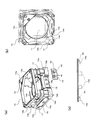
図2(a)は、ベース10の構成を示す斜視図、図2(b)は、ベース10を上側から見たときの斜視図、図2(c)は、ベース10の係止片16b近傍の部分を上側から見た図である。図示の如く、ベース10は、枠状の部材からなっている。ベース10には、光を通すための開口11が形成されている。また、ベース10の側面には、コイル20を巻き付けるためのコイル装着部12a、12bが、全周に亘って形成されている。
ベース10の上面にはシャフト保持部13が形成され、このシャフト保持部13に、シャフト90を圧入するための孔13aが形成されている。また、この孔13aと同軸となる位置に、シャフト90を圧入するための孔13bが形成されている。
また、同図(b)を参照して、ベース10の上面の、シャフト保持部13と対角の関係となる位置に、シャフトホルダ80が装着される受け部14が形成されている。この受け部14には、シャフトホルダ80の突起83(図3(a)参照)と嵌合する孔部14aが形成されている。また、受け部14の近傍には、シャフトホルダ80の鍔部81と係合する切り欠き14bが形成されている。さらに、受け部14の下方には、シャフト90が圧入される孔14cが形成されている。受け部14にシャフトホルダ80が装着されると、この孔14cが、シャフトホルダ80の孔82(図3(a)参照)と正対する。
同図(a)を参照して、ベース10の側面には、段部15が形成され、この段部15に係止片15aが形成されている。また、ベース10の他の側面には、凹部16が形成され、この凹部16に2つの突起16aが形成されている。凹部16の上方には、2つの係止片16bが形成されている。同図(c)に示す如く、2つの係止片16bは、それぞれ、右側に傾斜面を有する。コイル20をプリント基板40に装着する際には、この傾斜面にコイル20の中間部が係止される。
同図(a)に示す如く、プリント基板40には、2つの突起16aに対応する位置に2つの孔41が形成されている。また、孔41の周りから下端に掛けて、端子部42が外部に露出している。2つの孔41に突起16aを挿入させて、プリント基板40が凹部16に装着される。プリント基板40の装着方法の詳細については、追って、図3(c)を参照して説明する。
また、ベース10には、段部15の上方に、溝17が形成されている。この溝17は、後述のように磁性板31をコイル20の外側面に接着する際に、接着剤の溜まり溝として機能する。他の側面にも、他の磁性板32を接着する際の接着剤の溜まり溝として機能する溝18が形成されている(図4(b)参照)。また、ベース10の下部の4隅には、それぞれ、カバー100の足部103に当接する段部10aが形成されている。
組立時には、まず、図2(a)に示すベース10の凹部16にプリント基板40が装着される。さらに、コイル20が装着されて、コイル20の端部がプリント基板40に半田付けされる。その後、レンズと磁石70が装着されたホルダ60が、ベース10の上方からベース10の枠内に収容される。
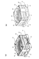
図3(a)は、ホルダ60がベース10に収容された状態を示す図である。図示の如く、コイル20の2つの端部20a、20bが、それぞれ、係止片16bを経由して、プリント基板40へと至っている。図中の矢印は、コイル20の巻き方向を示している。
図3(c)は、コイル20の端部20a、20bの装着状態を示す図である。凹部16にプリント基板40が嵌め込まれた後、コイル20の端部20aが、左側の突起16aに巻き付けられる。しかる後、端部20aが同図(a)に示す左側の係止片16bの傾斜面に掛けられて(図2(c)参照)、ベース10の下側のコイル装着部12bに時計方向(図3(a)の下側の矢印方向)に巻き付けられる。下側のコイル装着部12bへの巻き付けが終わると、コイル20が上側のコイル装着部12aに反時計方向(図3(a)の上側の矢印方向)に巻き付けられる。上側のコイル装着部12aへの巻き付けが終わると、コイル20の端部20bが右側の係止片16aの傾斜面に掛けられて(図2(c)参照)、図3(c)に示すように、右側の突起16aに巻き付けられる。しかる後、突起16aに巻き付けられた端部20a、20bと、各端部に対応する端子部42とを繋ぐように半田付けが行われる。こうして、コイル20と端子部42とが電気的に接続される。なお、半田付けにより、プリント基板40は凹部16から抜けないように留められる。この状態で、さらに、プリント基板40と凹部16とが接着固定されても良い。
しかる後、突部83をベース側の孔部14a(図2(b)参照)に嵌め込むようにして、シャフトホルダ80が受け部14に装着される。このとき、シャフトホルダ80の鍔部81が、ベース10上面の切り欠き14bに係合する。
図3(b)は、こうしてシャフトホルダ80が受け部14に装着された状態を示す図である。この状態において、孔13a、13bと、ホルダ60の孔62とを整合させ、一方のシャフト90を孔13aから圧入する。シャフト90の先端は、孔13aに圧入された後、孔62を通り、その後、孔13b(図2(a)参照)に圧入される。この状態では、シャフト90の後端が孔13aに支持される。こうして、一方のシャフト90のベース10に対する装着と、このシャフト90と孔62との係合が完了する。
さらに、この状態において、シャフトホルダ80の孔82と、ベース10の孔14c(図2(b)参照)と、ホルダ60の切り溝63(図1(a)参照)とを整合させ、他方のシャフト90を孔82から圧入する。シャフト90の先端は、孔82に圧入された後、切り溝63を通り、その後、孔13cに圧入される。この状態では、シャフト90の後端が孔82に支持される。こうして、他方のシャフト90のベース10に対する装着と、このシャフト90と切り溝63との係合が完了する。
このように2本のシャフト90が装着されることにより、ホルダ60が、レンズの光軸方向に変位可能となるように、ベース10に装着される。しかる後、コイル20の外側面に2つの磁性板31、32が接着される。
図4(a)、(b)は、磁性板31、32の装着状態を示す図である。同図(a)は、図1(b)と略同じアングルからレンズ駆動装置を見たときの斜視図、同図(b)は、同図(a)の状態からレンズ駆動装置をレンズの光軸を軸として反時計方向に略90度回転させた状態の斜視図である。同図(b)に示すように、コイル20の外側面には、磁性板31の他に磁性板32が接着される。同図(b)の2つの側面以外の他の側面には、磁性板は装着されていない。また、ベース10の磁性板32の近傍には溝18が形成されている。磁性板31、32の接着時には、溝17、18が、接着剤の溜まり溝として機能する。
このように2つの磁性板31、32を配置すると、これら磁性板31、32と、ホルダ60に配された磁石70(図1(a)参照)との間に磁力が働く。この磁力によって、ホルダ60の孔62と切り溝63(図1(a)参照)がシャフト90に押し付けられる。これにより、コイル20への通電が中止されたときに、ホルダ60が通電中止時の位置に保持されるようになる。
こうして磁性板31、32が装着された後、図1(b)に示すように、上方からカバー100がベースに装着される。このとき、カバーの鍔部102がベース10の段部15に嵌り込み、さらに、鍔部102の孔102aが段部15の係止片15aと係合する。また、カバー100の足部103がベース10の段部10aの上面に当接する。こうして、図1(c)に示すように、レンズ駆動装置の組み立てが完了する。かかる組立状態において、プリント基板40の端子部42は、カバー100によって覆われずに外部に露出する。
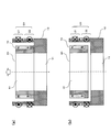
図5は、レンズ駆動装置の駆動動作を説明する図である。この図は、図4(a)のA-A’断面を模式的に示す図である。なお、図中、円に黒点のマークおよび円にバツのマークは、電流が流れる方向を示す。円に黒点のマークは図面参照者に向かってくる方向を示し、円にバツのマークは図面参照者から遠ざかる方向を示す。
図示のように、コイル20の上段部分21には、磁石70のN極の領域が対向し、下段部分22には、磁石70のS極の領域が対向している。コイル20に図5(a)に示す方向の電流が流れると、磁石70に図の上方向の推進力が作用し、レンズホルダ60は図の上方向に変位する。これにより、レンズホルダ60は、同図(b)に示すように、上方向に変位する。この状態で、電流の印加が中止されると、ホルダ60は、磁性板31、32と磁石70との間の磁力によってシャフト90に押し付けられ、電流印加中止時の位置に保持される。また、図7(b)の状態において、コイル20に逆方向の電流が印加されると、レンズホルダ60は下方向に変位される。
このようにして、レンズホルダ60が上方向と下方向に変位されることにより、レンズがオンフォーカス位置に位置づけられる。なお、レンズホルダ60のホームポジションは、レンズホルダ60の下面がベース10に当接する位置である。
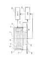
図6は、上記構成のレンズ駆動装置を搭載するカメラモジュールの概略構成を示す図である。図中、1がレンズ駆動装置である。
ベース10の下方には、イメージセンサ201が装着された回路基板200が配されている。また、ベース10には、位置センサとしてホール素子110が配され、ホール素子110からの信号をもとにレンズホルダ60の位置検出が行われる。
フォーカス動作時、CPU(Central Processing Unit)301は、ドライバ302を制御して、レンズホルダ60をホームポジションから予め定められた位置までレンズの光軸方向に変位させる。このとき、ホール素子110からの位置検出信号がCPU301に入力される。同時に、CPU301は、イメージセンサ201から入力される信号を処理して撮像画像のコンストラスト値を取得する。そして、このコンストラスト値が最良となるレンズホルダ60の位置をオンフォーカス位置として取得する。
その後、CPU301は、取得したオンフォーカス位置に向けてレンズホルダ60を駆動する。その際、CPU301は、ホール素子110からの信号をモニタし、ホール素子110からの信号がオンフォーカス位置に対応する状態になるまで、レンズホルダ60を駆動する。これにより、レンズホルダ60がオンフォーカス位置に位置づけられる。
図7は、回路基板200に対するレンズ駆動装置1の装着方法を説明する図である。同図(a)は、回路基板200にレンズ駆動装置1を装着する前の状態を示す斜視図、同図(b)は、レンズ駆動装置1を裏側から見た斜視図、同図(c)は、回路基板200にレンズ駆動装置1を装着する後の状態を示す斜視図である。
同図(b)に示すように、ベース10の下面には、対角の位置に、2つのピン19が形成されている。また、ベースの下面には、フィルタ50が装着された状態でイメージセンサ201を収容可能な深さの収容部Sが設けられている。凹部16は、前記ベースの側面の前記収容部に対応する位置に形成されている。また、同図(a)に示すように、回路基板200には、ベース10のピン19に対応する位置に、孔200aが形成されている。
レンズ駆動装置1は、同図(a)に示すように、上方から回路基板200に設置される。このとき、ベース10の2つのピン19が回路基板200の2つの孔200aに嵌め込まれる。これにより、イメージセンサ201に対してレンズ駆動装置1が正しく位置決めされる。この状態で、レンズ駆動装置1が回路基板200に接着固定される。これにより、同図(c)に示すように、回路基板200にレンズ駆動装置1が設置される。
本実施の形態によれば、ベース10の下面よりもプリント基板40の下端が突出しないため、ベース10と回路基板200との間に間隔を空ける必要が無い。よって、レンズの光軸方向におけるカメラモジュールの形状を小さくでき、カメラモジュールの外形をコンパクトにできる。
また、本実施の形態によれば、ベース10の収容部Sにイメージセンサ201が収容されるようにレンズ駆動装置1が回路基板200の上面に装着されるため、レンズの光軸方向におけるカメラモジュールの形状を一層小さくでき、カメラモジュールの外形をよりコンパストにできる。また、イメージセンサ201が、レンズ駆動装置1によって覆われるため、イメージセンサ201をレンズ駆動装置1によって保護することもできる。
また、本実施の形態によれば、図3(c)に示すように、突起16aにコイル20の端部20a、20bが巻き付けられるため、コイル20の始末を容易に行いながら、コイル20の端部20a、20bを、プリント基板40の端子部42の位置に位置づけることができる。また、突起16aの位置に半田を施すことにより、コイル20の端部20a、20bを対応する端子部42に容易に接続することができる。
また、本実施の形態によれば、図3(a)に示すように、2つの係止片16bにコイル16bの中間部が中継されるため、2つの端部20a、20bを、交差することなく円滑に、対応する端子部42に導くことができる。
さらに、本実施の形態によれば、図7(c)に示すように、端子部42が、カバー100に覆われることなく外部に露出するため、端子部42に対する信号線の装着を容易に行うことができる。なお、端子部42に対する信号線の装着は半田付けによって行われる。信号線は、図7(c)の状態で行っても良く、あるいは、レンズ駆動装置1を回路基板200に装着する前に行っても良い。
以上、本発明の実施の形態について説明したが、本発明は、上記実施の形態に何ら制限されるものではなく、また、本発明の実施形態も上記以外に種々の変更が可能である。
たとえば、上記実施の形態では、図7(c)に示すように、ベース10の下部をカバー100により覆わないようにすることで、端子部42を外部に露出させるようにしたが、ベース10の下部も全てカバー100で覆うようにし、カバー100の端子部42に対応する位置に切り欠きを設けて、端子部42を外部に露出させるようにしても良い。
また、上記実施の形態では、図3(a)に示すように、コイル20の端部20a、20bの中間部を、係止片16bに中継させるようにしたが、2つの係止片16bの何れか一方または両方を省略して、コイル20a、20bを直接、対応する突起16aに巻き付けるようにしても良い。また、2つの突起16aに巻き付ける前にベース10のコイル装着部12a、12bにコイル20を巻き付け、その後、プリント基板20を凹部16に装着して、コイルの端部20a、20bを突起16aに巻き付けるようにすることもできる。この場合、図2(c)に示す左側の係止片16bには、左側に傾斜面が形成され、この傾斜面にコイル20の端部20aが掛けられて、左側の突起16aに巻き付けられる。
また、上記実施の形態では、ホルダ60の一つの側面には一つの磁石70が配されたが、各側面に2つ以上の磁石を配置するようにしても良い。
また、上記実施の形態では、2つの磁性板31、32をベース10に配置するようにしたが、1つまたは3つ以上の磁性板をベース10に配置するようにしても良い。ただし、この場合も、上記実施の形態と同様、磁石と磁性板との間に生じる磁力がレンズの光軸に垂直な面内においてアンバランスとなるように、磁性板が配置されるのが望ましい。
さらに、ベース10やホルダ60等の形状も、上記に限られるものではなく、適宜変更が可能である。また、2本のシャフト90の径は同じでなくても良く、シャフト以外のガイド機構によって、ホルダ60がレンズの光軸方向に案内されるようにしても良い。
この他、本発明の実施の形態は、特許請求の範囲に示された技術的思想の範囲内において、適宜、種々の変更が可能である。
1 … レンズ駆動装置
10 … ベース
16 … 凹部
16a … 突起
16b … 係止片(係止部)
S … 収容部
20 … コイル
40 … プリント基板(端子基板)
41 … 孔
42 … 端子部
60 … ホルダ
70 … 磁石
100 … カバー
200 … 回路基板
201 … イメージセンサ(撮像素子)
301 … CPU(制御部)
10 … ベース
16 … 凹部
16a … 突起
16b … 係止片(係止部)
S … 収容部
20 … コイル
40 … プリント基板(端子基板)
41 … 孔
42 … 端子部
60 … ホルダ
70 … 磁石
100 … カバー
200 … 回路基板
201 … イメージセンサ(撮像素子)
301 … CPU(制御部)
Claims (6)
- ベースと、
レンズを保持するとともに前記ベースに対して前記レンズの光軸方向に変位可能に支持されたホルダと、
前記ホルダに装着された磁石と、
前記磁石に向き合うように前記ベースに装着されたコイルと、
前記コイルに電気的に接続されるとともに前記コイルに電流を印加するための端子部を備えた端子基板と、を備え、
前記ベースの側面に凹部が形成され、この凹部に下端がベース下面よりも突出しないように、前記端子基板が装着される、
ことを特徴とするレンズ駆動装置。 - 請求項1に記載のレンズ駆動装置において、
前記ベースの下面には、撮像素子を収容するための深さを有する収容部が形成され、
前記凹部は、前記ベースの側面の前記収容部に対応する位置に形成され、
前記凹部の上方の前記ベースの側面に、前記コイルが、前記レンズの光軸の周りに巻回されるようにして装着されている、
ことを特徴とするレンズ駆動装置。 - 請求項1に記載のレンズ駆動装置において、
前記凹部から前記ベースの側面に垂直な方向に突起が形成され、
前記端子基板には、前記突起に対応する位置に孔が形成され、
前記突起を前記孔に挿入するようにして前記端子基板が前記凹部内に位置づけられた状態で、前記突起に前記コイルの端部が巻き付けられ、
前記突起に巻き付けられた前記コイルの端部が前記端子部に半田付けされる、
ことを特徴とするレンズ駆動装置。 - 請求項3に記載のレンズ駆動装置において、
前記コイルが前記突起に至る前に前記コイルを中継させるための係止部が、前記ベースの前記凹部が形成された側面に形成されている、
ことを特徴とするレンズ駆動装置。 - 請求項1に記載のレンズ駆動装置において、
前記コイルが前記突起に至る前に前記コイルを中継させるための係止部が、前記ベースの前記凹部が形成された側面に形成されている、
ことを特徴とするレンズ駆動装置。 - 請求項2に記載のレンズ駆動装置と、
前記レンズによって集光された光を受光する撮像素子と、
前記撮像素子が装着された回路基板と、
前記コイルに制御信号を印加するための制御部と、を備え、
前記収容部に前記撮像素子が収容されるようにして、前記レンズ駆動装置が前記回路基板に設置される、
ことを特徴とするカメラモジュール。
Priority Applications (1)
| Application Number | Priority Date | Filing Date | Title |
|---|---|---|---|
| JP2012503090A JPWO2011108430A1 (ja) | 2010-03-04 | 2011-02-24 | レンズ駆動装置およびカメラモジュール |
Applications Claiming Priority (2)
| Application Number | Priority Date | Filing Date | Title |
|---|---|---|---|
| JP2010047287 | 2010-03-04 | ||
| JP2010-047287 | 2010-03-04 |
Publications (1)
| Publication Number | Publication Date |
|---|---|
| WO2011108430A1 true WO2011108430A1 (ja) | 2011-09-09 |
Family
ID=44542084
Family Applications (1)
| Application Number | Title | Priority Date | Filing Date |
|---|---|---|---|
| PCT/JP2011/054093 Ceased WO2011108430A1 (ja) | 2010-03-04 | 2011-02-24 | レンズ駆動装置およびカメラモジュール |
Country Status (2)
| Country | Link |
|---|---|
| JP (1) | JPWO2011108430A1 (ja) |
| WO (1) | WO2011108430A1 (ja) |
Cited By (4)
| Publication number | Priority date | Publication date | Assignee | Title |
|---|---|---|---|---|
| EP2690162A1 (en) | 2012-07-24 | 2014-01-29 | Fundacion Tecnalia Research & Innovation | Equipment for treating gases and use of said equipment for treating a synthesis gas contaminated with tars |
| JP2015099274A (ja) * | 2013-11-19 | 2015-05-28 | 日本電産コパル株式会社 | レンズ駆動装置 |
| EP2863624A3 (en) * | 2013-10-16 | 2015-08-05 | Samsung Electro-Mechanics Co., Ltd. | Camera module, method for aligning optical axis of camera module and portable electronic device including camera module |
| JP6964262B1 (ja) * | 2020-07-22 | 2021-11-10 | 株式会社アルファラボ・ソリューション | レンズ移動機構及び撮像装置 |
Citations (4)
| Publication number | Priority date | Publication date | Assignee | Title |
|---|---|---|---|---|
| JP2006078869A (ja) * | 2004-09-10 | 2006-03-23 | Nidec Sankyo Corp | レンズ駆動装置 |
| JP2006350019A (ja) * | 2005-06-16 | 2006-12-28 | Shicoh Eng Co Ltd | レンズ駆動装置 |
| JP2008116925A (ja) * | 2006-11-01 | 2008-05-22 | Fuzhun Precision Industry (Shenzhen) Co Ltd | 2段式焦点調節構造 |
| JP2009216878A (ja) * | 2008-03-10 | 2009-09-24 | Mitsumi Electric Co Ltd | レンズ駆動装置およびカメラモジュール |
Family Cites Families (2)
| Publication number | Priority date | Publication date | Assignee | Title |
|---|---|---|---|---|
| JP2008216927A (ja) * | 2007-03-07 | 2008-09-18 | Sanyo Electric Co Ltd | レンズ駆動装置 |
| JP4642053B2 (ja) * | 2007-09-14 | 2011-03-02 | 三洋電機株式会社 | レンズ駆動装置 |
-
2011
- 2011-02-24 JP JP2012503090A patent/JPWO2011108430A1/ja active Pending
- 2011-02-24 WO PCT/JP2011/054093 patent/WO2011108430A1/ja not_active Ceased
Patent Citations (4)
| Publication number | Priority date | Publication date | Assignee | Title |
|---|---|---|---|---|
| JP2006078869A (ja) * | 2004-09-10 | 2006-03-23 | Nidec Sankyo Corp | レンズ駆動装置 |
| JP2006350019A (ja) * | 2005-06-16 | 2006-12-28 | Shicoh Eng Co Ltd | レンズ駆動装置 |
| JP2008116925A (ja) * | 2006-11-01 | 2008-05-22 | Fuzhun Precision Industry (Shenzhen) Co Ltd | 2段式焦点調節構造 |
| JP2009216878A (ja) * | 2008-03-10 | 2009-09-24 | Mitsumi Electric Co Ltd | レンズ駆動装置およびカメラモジュール |
Cited By (7)
| Publication number | Priority date | Publication date | Assignee | Title |
|---|---|---|---|---|
| EP2690162A1 (en) | 2012-07-24 | 2014-01-29 | Fundacion Tecnalia Research & Innovation | Equipment for treating gases and use of said equipment for treating a synthesis gas contaminated with tars |
| EP2863624A3 (en) * | 2013-10-16 | 2015-08-05 | Samsung Electro-Mechanics Co., Ltd. | Camera module, method for aligning optical axis of camera module and portable electronic device including camera module |
| US10194062B2 (en) | 2013-10-16 | 2019-01-29 | Samsung Electro-Mechanics Co., Ltd. | Camera module, method for aligning optical axis of camera module and portable electronic device including camera module |
| JP2015099274A (ja) * | 2013-11-19 | 2015-05-28 | 日本電産コパル株式会社 | レンズ駆動装置 |
| JP6964262B1 (ja) * | 2020-07-22 | 2021-11-10 | 株式会社アルファラボ・ソリューション | レンズ移動機構及び撮像装置 |
| WO2022019210A1 (ja) * | 2020-07-22 | 2022-01-27 | 株式会社アルファラボ・ソリューション | レンズ移動機構及び撮像装置 |
| JP2022021757A (ja) * | 2020-07-22 | 2022-02-03 | 株式会社アルファラボ・ソリューション | レンズ移動機構及び撮像装置 |
Also Published As
| Publication number | Publication date |
|---|---|
| JPWO2011108430A1 (ja) | 2013-06-27 |
Similar Documents
| Publication | Publication Date | Title |
|---|---|---|
| CN107111098B (zh) | 透镜驱动装置、摄像机模块、以及摄像机搭载装置 | |
| CN103226233B (zh) | 透镜架驱动装置 | |
| CN103226232B (zh) | 透镜架驱动装置 | |
| TWI708112B (zh) | 透鏡驅動裝置、相機模組以及相機搭載裝置 | |
| CN107615125B (zh) | 透镜驱动装置、摄像机模块、以及摄像机搭载装置 | |
| CN107111093B (zh) | 透镜驱动装置、摄像机模块、以及摄像机搭载装置 | |
| CN105319664B (zh) | 透镜移动器件、摄像头模块和光学装置 | |
| US7492538B2 (en) | Camera module | |
| TWI468769B (zh) | 3d立體電路導腳結合簧片之結構 | |
| CN102819087B (zh) | 透镜驱动装置、自动对焦照相机及附带照相机的移动终端 | |
| US10551589B2 (en) | Lens drive device, camera module, and camera mounting device | |
| JP3921467B2 (ja) | カメラモジュール、カメラモジュールの製造方法、電子機器及び電子機器の製造方法 | |
| KR102608087B1 (ko) | 렌즈 구동 장치, 카메라 모듈, 및 카메라 탑재 장치 | |
| CN106537215A (zh) | 透镜架驱动装置和搭载有摄像机移动终端 | |
| JP2010061030A (ja) | レンズ駆動装置 | |
| TW201030370A (en) | Image blur correction device, imaging lens unit, and camera unit | |
| CN108603993A (zh) | 透镜驱动装置、摄像机模块及摄像机搭载装置 | |
| CN115327734A (zh) | 透镜驱动装置 | |
| CN101533146A (zh) | 透镜驱动装置及相机模块 | |
| KR20180002077A (ko) | 카메라 모듈 | |
| KR20120117236A (ko) | 자동초점 기능을 갖는 카메라 모듈 | |
| WO2011105470A1 (ja) | レンズ駆動装置およびカメラモジュール | |
| JP2010276850A (ja) | レンズ駆動装置 | |
| JPWO2011108430A1 (ja) | レンズ駆動装置およびカメラモジュール | |
| JP2010085448A (ja) | 像振れ補正装置、撮像レンズユニット、及びカメラユニット |
Legal Events
| Date | Code | Title | Description |
|---|---|---|---|
| 121 | Ep: the epo has been informed by wipo that ep was designated in this application |
Ref document number: 11750540 Country of ref document: EP Kind code of ref document: A1 |
|
| WWE | Wipo information: entry into national phase |
Ref document number: 2012503090 Country of ref document: JP |
|
| NENP | Non-entry into the national phase |
Ref country code: DE |
|
| 122 | Ep: pct application non-entry in european phase |
Ref document number: 11750540 Country of ref document: EP Kind code of ref document: A1 |