WO2011105433A1 - 発光デバイス - Google Patents
発光デバイス Download PDFInfo
- Publication number
- WO2011105433A1 WO2011105433A1 PCT/JP2011/053999 JP2011053999W WO2011105433A1 WO 2011105433 A1 WO2011105433 A1 WO 2011105433A1 JP 2011053999 W JP2011053999 W JP 2011053999W WO 2011105433 A1 WO2011105433 A1 WO 2011105433A1
- Authority
- WO
- WIPO (PCT)
- Prior art keywords
- light
- light emitting
- emitting device
- emitting element
- cavity
- Prior art date
- Legal status (The legal status is an assumption and is not a legal conclusion. Google has not performed a legal analysis and makes no representation as to the accuracy of the status listed.)
- Ceased
Links
Images



Classifications
-
- H—ELECTRICITY
- H10—SEMICONDUCTOR DEVICES; ELECTRIC SOLID-STATE DEVICES NOT OTHERWISE PROVIDED FOR
- H10H—INORGANIC LIGHT-EMITTING SEMICONDUCTOR DEVICES HAVING POTENTIAL BARRIERS
- H10H20/00—Individual inorganic light-emitting semiconductor devices having potential barriers, e.g. light-emitting diodes [LED]
- H10H20/80—Constructional details
- H10H20/85—Packages
- H10H20/852—Encapsulations
- H10H20/854—Encapsulations characterised by their material, e.g. epoxy or silicone resins
-
- H—ELECTRICITY
- H10—SEMICONDUCTOR DEVICES; ELECTRIC SOLID-STATE DEVICES NOT OTHERWISE PROVIDED FOR
- H10H—INORGANIC LIGHT-EMITTING SEMICONDUCTOR DEVICES HAVING POTENTIAL BARRIERS
- H10H20/00—Individual inorganic light-emitting semiconductor devices having potential barriers, e.g. light-emitting diodes [LED]
- H10H20/80—Constructional details
- H10H20/85—Packages
- H10H20/851—Wavelength conversion means
- H10H20/8516—Wavelength conversion means having a non-uniform spatial arrangement or non-uniform concentration, e.g. patterned wavelength conversion layer or wavelength conversion layer with a concentration gradient
-
- H—ELECTRICITY
- H10—SEMICONDUCTOR DEVICES; ELECTRIC SOLID-STATE DEVICES NOT OTHERWISE PROVIDED FOR
- H10H—INORGANIC LIGHT-EMITTING SEMICONDUCTOR DEVICES HAVING POTENTIAL BARRIERS
- H10H20/00—Individual inorganic light-emitting semiconductor devices having potential barriers, e.g. light-emitting diodes [LED]
- H10H20/80—Constructional details
- H10H20/85—Packages
- H10H20/855—Optical field-shaping means, e.g. lenses
- H10H20/856—Reflecting means
-
- H—ELECTRICITY
- H10—SEMICONDUCTOR DEVICES; ELECTRIC SOLID-STATE DEVICES NOT OTHERWISE PROVIDED FOR
- H10H—INORGANIC LIGHT-EMITTING SEMICONDUCTOR DEVICES HAVING POTENTIAL BARRIERS
- H10H20/00—Individual inorganic light-emitting semiconductor devices having potential barriers, e.g. light-emitting diodes [LED]
- H10H20/80—Constructional details
- H10H20/882—Scattering means
Definitions
- the present invention relates to a light emitting device including a light emitting element such as an LED (Light Emitting Diode).
- a light emitting element such as an LED (Light Emitting Diode).
- this type of light emitting device includes a light emitting element (101) such as an LED and a package (100) for mounting the light emitting element (101) (for example, Patent Document 1). reference).
- the package (100) includes a ceramic base (102) and a ceramic frame (103), and the frame (103) is joined and integrated with the upper surface (102a) of the base (102).
- a cavity (103a) for accommodating the light emitting element (101) is formed.
- the light emitting element (101) is accommodated in the cavity (103a) of the package (100), and the die attach pad (107) It is installed through.
- the cavity (103a) is filled with a resin material (108) containing a phosphor.
- the phosphor receives light emitted from the light emitting element (101) and emits new light (fluorescence) having a wavelength different from that of the light. Therefore, the light emitting device emits light generated by mixing light of the light emitting element (101) and fluorescence.
- the phosphor concentration in the resin material (108) is uneven. For this reason, color unevenness is likely to occur in the light emitted from the light emitting device.
- an object of the present invention is to provide a light emitting device capable of emitting light with less color unevenness.
- a light-emitting device includes a light-emitting element and a package for mounting the light-emitting element.
- the package has a cavity, and the light-emitting element is accommodated in the cavity.
- a phosphor layer containing one or more kinds of phosphors is formed on the bottom surface of the cavity, while the cavity covers the light emitting element, and the light emitted from the light emitting element and A light diffusion layer for diffusing light emitted from the phosphor in the phosphor layer is formed.
- the light emitting device In the light emitting device, light is emitted from the light emitting element in all directions. Of the light emitted from the light emitting element, the light traveling upward enters the light diffusion layer and is diffused by the light diffusion layer, so that a part of the light passes through the light diffusion layer upward. On the other hand, the remaining light is reflected by the light diffusion layer and travels downward, and then enters the phosphor layer. In addition, light emitted from the light emitting element obliquely downward is also incident on the phosphor layer.
- the phosphor in the phosphor layer receives light from the light-emitting element and emits new light (fluorescence) having a wavelength different from that of the light. The light emitted from the phosphor travels upward, enters the light diffusion layer, and is diffused by the light diffusion layer. Then, a part of the fluorescence travels upward through the light diffusion layer.
- the light emitting device light and fluorescence of the light emitting element are diffused by the light diffusion layer. Therefore, the light of the light emitting element and the fluorescence are mixed evenly, and as a result, light with less color unevenness is emitted from the light emitting device.
- the light diffusion layer extends to the inner peripheral surface of the cavity, and the outer peripheral edge of the light diffusion layer is in contact with the inner peripheral surface. Thereby, the light and fluorescence of the light emitting element are efficiently diffused by the light diffusion layer.
- the cavity may be filled with a light diffusing agent, and the light diffusing layer may be formed by the light diffusing agent.
- Another light-emitting device includes a substrate and a light-emitting element installed on the surface of the substrate, and a phosphor layer containing one or more types of phosphors is formed on the surface of the substrate.
- a light diffusing layer is formed on the surface of the base so as to cover the light emitting element and diffuse light emitted from the light emitting element and light emitted from the phosphor in the phosphor layer.
- light traveling in all directions from the light emitting element the light traveling toward the light diffusion layer is incident on the light diffusion layer and diffused by the light diffusion layer, Some of the light passes through the light diffusion layer, while the remaining light is reflected by the light diffusion layer and enters the phosphor layer.
- light emitted from the light emitting element toward the phosphor layer also enters the phosphor layer.
- the phosphor in the phosphor layer receives light from the light-emitting element and emits new light (fluorescence) having a wavelength different from that of the light.
- the light emitted from the phosphor travels toward the light diffusion layer, enters the light diffusion layer, and is diffused by the light diffusion layer. A part of the fluorescence passes through the light diffusion layer.
- the other light emitting device light and fluorescence of the light emitting element are diffused by the light diffusion layer. Therefore, the light of the light emitting element and the fluorescence are mixed evenly, and as a result, light with less color unevenness is emitted from the light emitting device.
- the light emitting device can emit light with little color unevenness.
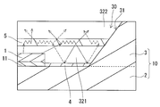
- FIG. 1 is a cross-sectional view showing a light emitting device according to an embodiment of the present invention.
- FIG. 2 is a cross-sectional view for explaining a path of light emitted from the LED.
- FIG. 3 is a cross-sectional view showing a first modification of the light emitting device.
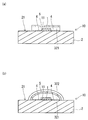
- FIG. 4A is a cross-sectional view illustrating an example of a second modification of the light emitting device, and
- FIG. 4B is a cross-sectional view illustrating another example of the second modification.
- FIG. 5 is a cross-sectional view illustrating a conventional light emitting device.
- FIG. 1 is a cross-sectional view showing a light emitting device according to an embodiment of the present invention.
- the light emitting device of the present embodiment includes an LED (1) and a package (10) for mounting the LED (1).
- the package (10) is composed of a ceramic base (2) and a ceramic frame (3), and the frame (3) is joined and integrated with the upper surface (21) of the base (2). .
- a cavity (30) for accommodating the LED (1) is formed from the inner peripheral surface (31) of the frame (3) and the upper surface (21) of the base body (2).
- the cavity (30) is recessed in the package (10).
- the ceramic material constituting the substrate (2) and the frame (3) may be a metal material having thermal conductivity and / or conductivity (for example, silver (Ag) or silver (Ag)).
- low temperature co-fired ceramic (LTCC) capable of co-firing with (platinum (Pt) alloy).
- LTCC low-temperature co-fired ceramic
- metal materials such as silver and an alloy, are used as a heat conductive material of a thermal via (not shown) formed on the base body (2), for example, in order to improve heat dissipation of the light emitting device.
- the LED (1) is installed on the bottom surface (33) of the cavity (30) via the die attach pad (11).
- the LED (1) emits light in all directions.
- a phosphor layer (4) containing one or more kinds of phosphors is formed in a region different from the region where the die attach pad (11) is installed.
- a first resin layer (321) that also covers the surface of the LED (1) is formed on the phosphor layer (4), and on the first resin layer (321), A second resin layer (322) exposed on the upper surface (34) of the frame (3) is formed.
- the 1st resin layer (321) and the 2nd resin layer (322) are formed from the resin material which does not contain fluorescent substance.
- a light diffusion layer (5) is interposed between the first resin layer (321) and the second resin layer (322), and the light diffusion layer (5) is an LED ( 1) covering the LED (1) and extending from the region on the LED (1) to the inner peripheral surface (31) of the cavity (30), and the outer peripheral edge of the light diffusion layer (5) is in contact with the inner peripheral surface (31) is doing.
- the light diffusing layer (5) is formed of a light diffusing agent having a low light absorption rate and a high light reflectance, such as ceramic powder, and the light emitted from the LED (1) and the phosphor layer (4 ) Diffuse the light emitted from the phosphor inside.
- FIG. 2 is a cross-sectional view for explaining the path of light emitted from the LED (1).
- light emitted from the LED (1) is indicated by a solid arrow
- light emitted from the phosphor is indicated by a broken arrow.
- the light traveling upward from the light emitted from the LED (1) enters the light diffusion layer (5) and is diffused by the light diffusion layer (5).
- a part of the light passes upward through the light diffusion layer (5), while the remaining light is reflected by the light diffusion layer (5) and travels downward, and then enters the phosphor layer (4).
- light (not shown) emitted diagonally downward from the light of the LED (1) also enters the phosphor layer (4).
- the phosphor in the phosphor layer (4) receives light from the LED (1) and emits new light (fluorescence) having a wavelength different from that of the light.
- the light emitted from the phosphor travels upward, enters the light diffusion layer (5), and is diffused by the light diffusion layer (5). Then, a part of the fluorescence travels upward through the light diffusion layer (5).
- the light and fluorescence of the LED (1) are diffused by the light diffusion layer (5).
- the light diffusion layer (5) extends from the region on the LED (1) to the inner peripheral surface (31) of the cavity (30), and the light diffusion layer is formed on the inner peripheral surface (31).
- the outer peripheral edge of (5) is in contact.
- the light and fluorescence of the LED (1) are efficiently diffused by the light diffusion layer (5). Therefore, as shown in FIG. 2, the light (solid arrow) of the LED (1) and the fluorescence (broken arrow) are mixed evenly, and as a result, light with less color unevenness is emitted from the light emitting device. become.
- BN boron nitride
- BN boron nitride
- has good thermal conductivity BN: 30 to 60 W / mK, silicon: 0.024 to 0.31 W / mK
- heat does not flow in the light diffusion layer (5).
- FIG. 3 is a cross-sectional view showing a first modification of the light emitting device.
- the first resin layer (321) and the second resin layer (322) are not provided, and the cavity (30) has a low light absorption rate such as ceramic powder.
- the light diffusion layer (5) may be formed over the entire cavity (30) by filling a light dispersing agent having a high light reflectance. Also in the light emitting device according to this modification, the light and the fluorescence of the LED (1) are efficiently diffused by the light diffusion layer (5), as in the light emitting device shown in FIG. Therefore, light with little color unevenness is emitted also from the light emitting device according to this modification.
- FIG. 4A is a cross-sectional view showing an example of the second modification of the light emitting device
- FIG. 4B is a cross-sectional view showing another example of the second modification.
- the said light emitting device may have a structure without a frame (3).
- the second resin layer (322) is not formed on the light diffusion layer (5).
- the second resin layer (322) may be formed on the light diffusion layer (5).
- the light diffusion layer (5) is curved in a dome shape, so that the outer peripheral edge of the light diffusion layer (5) is the base ( It may be in contact with the upper surface (21) of 2).
- the light and fluorescence of the LED (1) are diffused by the light diffusion layer (5), as in the light emitting device shown in FIG. Therefore, light with little color unevenness is emitted also from the light emitting device according to the second modification.
- the light emitting device having the structure without the frame (3) that is, the light emitting device having the structure without the cavity (30) has the cavity (30).
- the directivity of emitted light is lowered. Therefore, as shown in FIGS. 4A and 4B, the light emitting device is preferably applied to, for example, a lighting device that illuminates a room over a wide range.
- each part of the present invention is not limited to the above-described embodiment, and various modifications can be made within the technical scope described in the claims.
- the ceramic material, the light diffusing agent, and the like employed in the light emitting device are not limited to the materials described in the above embodiment, and various materials can be employed.
- adopted as the said light-emitting device are applicable also to the light-emitting device provided with light-emitting elements other than LED.
- LED light emitting device
- Substrate Frame (30) Cavity (31) Inner peripheral surface (33) Bottom (4) Phosphor layer (5) Light diffusion layer
Landscapes
- Led Device Packages (AREA)
Abstract
【課題】色むらの少ない光を出射することが可能な発光デバイスを提供する。 【解決手段】本発明に係る発光デバイスは、発光素子1と、該発光素子1を搭載するためのパッケージ10とを具え、該パッケージ10にはキャビティ30が凹設され、該キャビティ30に発光素子1が収容されている。ここで、キャビティ30の底面33には、1種又は複数種の蛍光体を含む蛍光体層4が形成される一方、キャビティ30内には、発光素子1を覆って、該発光素子1から発せられる光及び蛍光体層4中の蛍光体から発せられる光を拡散する光拡散層5が形成されている。
Description
本発明は、LED(Light Emitting Diode)等の発光素子を具えた発光デバイスに関する。
この種の発光デバイスは、図5に示す様に、LED等の発光素子(101)と、該発光素子(101)を搭載するためのパッケージ(100)とを具えている(例えば、特許文献1参照)。該パッケージ(100)は、セラミック製の基体(102)と、セラミック製の枠体(103)とから構成され、枠体(103)が基体(102)の上面(102a)に接合一体化されることにより、発光素子(101)を収容するためのキャビティ(103a)が形成されている。発光素子(101)は、パッケージ(100)のキャビティ(103a)に収容されて、基体(102)の上面(102a)の内、キャビティ(103a)の底面となる領域に、ダイアタッチパッド(107)を介して設置されている。
従来、上記発光デバイスにおいて、キャビティ(103a)内には、蛍光体を含む樹脂材(108)が充填されていた。蛍光体は、発光素子(101)から発せられた光を受けて該光とは波長が異なる新たな光(蛍光)を発する。従って、発光デバイスからは、発光素子(101)の光と蛍光とが混ざり合って生成された光が出射されることになる。
しかしながら、従来の発光デバイスにおいては、樹脂材(108)中の蛍光体の濃度にむらが生じていた。このため、発光デバイスから出射される光には、色むらが発生し易かった。
そこで本発明の目的は、色むらの少ない光を出射することが可能な発光デバイスを提供することである。
本発明に係る発光デバイスは、発光素子と、該発光素子を搭載するためのパッケージとを具え、該パッケージにはキャビティが凹設され、該キャビティに前記発光素子が収容されている。ここで、前記キャビティの底面には、1種又は複数種の蛍光体を含む蛍光体層が形成される一方、前記キャビティ内には、前記発光素子を覆って、該発光素子から発せられる光及び前記蛍光体層中の蛍光体から発せられる光を拡散する光拡散層が形成されている。
上記発光デバイスにおいては、発光素子から全方位に光が発せられる。発光素子から発せられた光の内、上方に向けて進行する光は、光拡散層に入射して該光拡散層によって拡散されることにより、その一部の光が光拡散層を上方へ通過する一方、残りの光が、光拡散層で反射されて下方へ進行した後、蛍光体層に入射する。又、発光素子の光の内、斜め下方に向けて出射された光も、蛍光体層に入射する。ここで、蛍光体層中の蛍光体は、発光素子の光を受けて該光とは波長が異なる新たな光(蛍光)を発する。蛍光体から発せられた光は、上方に進行して光拡散層に入射し、該光拡散層により拡散される。そして、一部の蛍光が光拡散層を通過して上方へ進行することになる。
よって、上記発光デバイスによれば、発光素子の光と蛍光とが光拡散層により拡散されることになる。従って、発光素子の光と蛍光とがむらなく混ざり合い、その結果、発光デバイスからは、色むらの少ない光が出射されることになる。
上記発光デバイスの具体的構成において、前記光拡散層は前記キャビティの内周面まで拡がり、該内周面に光拡散層の外周縁が接触している。これにより、発光素子の光及び蛍光が、光拡散層により効率良く拡散されることになる。
上記発光デバイスにおいて、前記キャビティ内には光拡散剤が充填され、該光拡散剤により前記光拡散層が形成されていてもよい。
本発明に係る他の発光デバイスは、基体と、該基体の表面に設置された発光素子とを具え、前記基体の表面には、1種又は複数種の蛍光体を含む蛍光体層が形成される一方、前記基体の表面上には、前記発光素子を覆って、該発光素子から発せられる光及び前記蛍光体層中の蛍光体から発せられる光を拡散する光拡散層が形成されている。
上記他の発光デバイスにおいては、発光素子から全方位に発せられた光の内、光拡散層に向けて進行する光は、光拡散層に入射して該光拡散層によって拡散されることにより、その一部の光が光拡散層を通過する一方、残りの光が、光拡散層で反射されて蛍光体層に入射する。又、発光素子の光の内、蛍光体層に向けて出射された光も、蛍光体層に入射する。ここで、蛍光体層中の蛍光体は、発光素子の光を受けて該光とは波長が異なる新たな光(蛍光)を発する。蛍光体から発せられた光は、光拡散層に向けて進行して光拡散層に入射し、該光拡散層により拡散される。そして、一部の蛍光が光拡散層を通過することになる。
よって、上記他の発光デバイスによれば、発光素子の光と蛍光とが光拡散層により拡散されることになる。従って、発光素子の光と蛍光とがむらなく混ざり合い、その結果、発光デバイスからは、色むらの少ない光が出射されることになる。
本発明に係る発光デバイスは、色むらの少ない光を出射することが出来る。
以下、本発明の実施の形態につき、図面に沿って具体的に説明する。
図1は、本発明の一実施形態に係る発光デバイスを示す断面図である。図1に示す様に、本実施形態の発光デバイスは、LED(1)と、該LED(1)を搭載するためのパッケージ(10)とを具えている。
パッケージ(10)は、セラミック製の基体(2)と、セラミック製の枠体(3)とから構成され、枠体(3)が基体(2)の上面(21)に接合一体化されている。これにより、枠体(3)の内周面(31)と基体(2)の上面(21)とから、LED(1)を収容するためのキャビティ(30)が形成されている。斯くして、パッケージ(10)には、キャビティ(30)が凹設されている。
上記パッケージ(10)において、基体(2)及び枠体(3)を構成するセラミック材には、熱伝導性及び/又は導電性を有する金属材料(例えば、銀(Ag)や、銀(Ag)と白金(Pt)の合金)との同時焼成が可能な低温同時焼成セラミック(LTCC)が用いられている。本実施形態においては、低温同時焼成セラミック(LTCC)として、アルミナとガラスが所定の割合で含まれたものが用いられている。尚、銀や合金等の金属材料は、例えば発光デバイスの放熱性を高めるべく基体(2)に形成されるサーマルビア(図示せず)の熱伝導材として用いられる。
LED(1)は、キャビティ(30)の底面(33)上に、ダイアタッチパッド(11)を介して設置されている。LED(1)からは、全方位に光が発せられることになる。
キャビティ(30)の底面(33)の内、ダイアタッチパッド(11)の設置領域とは異なる領域には、1種又は複数種の蛍光体を含む蛍光体層(4)が形成されている。又、キャビティ(30)内において、蛍光体層(4)上に、LED(1)の表面をも被覆した第1樹脂層(321)が形成され、該第1樹脂層(321)上に、枠体(3)の上面(34)に露出した第2樹脂層(322)が形成されている。ここで、第1樹脂層(321)及び第2樹脂層(322)は、蛍光体を含まない樹脂材から形成されている。
図1に示す様に、第1樹脂層(321)と第2樹脂層(322)との間には、光拡散層(5)が介在しており、光拡散層(5)は、LED(1)を覆って、該LED(1)上の領域からキャビティ(30)の内周面(31)まで拡がっており、該内周面(31)に光拡散層(5)の外周縁が接触している。ここで、光拡散層(5)は、セラミックパウダー等、光吸収率が低くて且つ光反射率の高い光拡散剤から形成されており、LED(1)から発せられる光及び蛍光体層(4)中の蛍光体から発せられる光を拡散する。
図2は、LED(1)から発せられる光の経路を説明するための断面図である。尚、図2では、LED(1)から発せられた光を実線矢印によって示し、蛍光体から発せられた光を破線矢印により示している。
図2に示す様に、LED(1)から発せられた光の内、上方に向けて進行する光は、光拡散層(5)に入射して該光拡散層(5)によって拡散されることにより、その一部の光が光拡散層(5)を上方へ通過する一方、残りの光が、光拡散層(5)で反射されて下方へ進行した後、蛍光体層(4)に入射する。又、LED(1)の光の内、斜め下方に向けて出射された光(図示せず)も、蛍光体層(4)に入射する。ここで、蛍光体層(4)中の蛍光体は、LED(1)の光を受けて該光とは波長が異なる新たな光(蛍光)を発する。蛍光体から発せられた光は、上方に進行して光拡散層(5)に入射し、該光拡散層(5)により拡散される。そして、一部の蛍光が光拡散層(5)を通過して上方へ進行することになる。
よって、上記発光デバイスによれば、LED(1)の光と蛍光とが光拡散層(5)により拡散されることになる。ここで、上記発光デバイスにおいては、光拡散層(5)が、LED(1)上の領域からキャビティ(30)の内周面(31)まで拡がり、該内周面(31)に光拡散層(5)の外周縁が接触している。このため、LED(1)の光及び蛍光が、光拡散層(5)により効率良く拡散されることになる。従って、図2に示す様に、LED(1)の光(実線矢印)と蛍光(破線矢印)とがむらなく混ざり合い、その結果、発光デバイスからは、色むらの少ない光が出射されることになる。
具体例として、LEDから発せられる光が青色であり、蛍光体から発せられる光が黄色である場合、上記発光デバイスからは、色むらの少ない白色の光が出射されることになる。
また、光拡散層(5)の中に、BN(ボロンナイトライド)を混入させる。ここで、BN(ボロンナイトライド)は熱伝導率が良いため、(BN:30~60W/mK、シリコン:0.024~0.31W/mK)、光拡散層(5)の中に熱が籠らずその他に部材に拡散しやすくなる。
図3は、上記発光デバイスの第1変形例を示した断面図である。図3に示す様に、上記発光デバイスにおいて、第1樹脂層(321)及び第2樹脂層(322)を設けずに、キャビティ(30)内に、セラミックパウダー等、光吸収率が低くて且つ光反射率の高い光分散剤を充填することにより、キャビティ(30)全域に光拡散層(5)を形成してもよい。本変形例に係る発光デバイスにおいても、図1に示す発光デバイスと同様、LED(1)の光と蛍光とが光拡散層(5)により効率良く拡散されることになる。従って、本変形例に係る発光デバイスからも、色むらの少ない光が出射されることになる。
図4(a)は、上記発光デバイスの第2変形例の一例を示した断面図であり、図4(b)は、該第2変形例の他の例を示した断面図である。図4(a)に示す様に、上記発光デバイスは、枠体(3)のない構成を有していてもよい。尚、図4(a)に示す発光デバイスでは、光拡散層(5)上に第2樹脂層(322)が形成されていない。勿論、枠体(3)のない構成において、光拡散層(5)上に第2樹脂層(322)が形成されていてもよい。又、図4(b)に示す様に、枠体(3)のない構成において、光拡散層(5)がドーム状に湾曲することにより、該光拡散層(5)の外周縁が基体(2)の上面(21)に接触していてもよい。
上記第2変形例に係る発光デバイスによれば、図1に示す発光デバイスと同様、LED(1)の光と蛍光とが光拡散層(5)により拡散されることになる。よって、第2変形例に係る発光デバイスからも、色むらの少ない光が出射されることになる。
一方、図4(a)及び図4(b)に示す様に枠体(3)のない構成を有する発光デバイス、即ちキャビティ(30)のない構成を有する発光デバイスは、キャビティ(30)を有する発光デバイス(図1参照)に比べて、出射される光の指向性が低くなる。従って、図4(a)及び図4(b)に示す如く発光デバイスは、例えば室内を広範囲に亘って照明する照明装置に適用することが好ましい。
尚、本発明の各部構成は上記実施の形態に限らず、特許請求の範囲に記載の技術的範囲内で種々の変形が可能である。例えば、上記発光デバイスに採用したセラミック材、光拡散剤等には、上記実施形態で説明した材料に限らず、種々の材料を採用することが出来る。又、上記発光デバイスに採用した各種構成は、LED以外の発光素子を具えた発光デバイスにも適用することが可能である。
(1) LED(発光素子)
(10) パッケージ
(2) 基体
(3) 枠体
(30) キャビティ
(31) 内周面
(33) 底面
(4) 蛍光体層
(5) 光拡散層
(10) パッケージ
(2) 基体
(3) 枠体
(30) キャビティ
(31) 内周面
(33) 底面
(4) 蛍光体層
(5) 光拡散層
Claims (5)
- 発光素子と、該発光素子を搭載するためのパッケージとを具え、該パッケージにはキャビティが凹設され、該キャビティに前記発光素子が収容されている発光デバイスにおいて、前記キャビティの底面には、1種又は複数種の蛍光体を含む蛍光体層が形成される一方、前記キャビティ内には、前記発光素子を覆って、該発光素子から発せられる光及び前記蛍光体層中の蛍光体から発せられる光を拡散する光拡散層が形成されていることを特徴とする発光デバイス。
- 前記光拡散層は前記キャビティの内周面まで拡がり、該内周面に光拡散層の外周縁が接触している請求項1に記載の発光デバイス。
- 前記キャビティ内には光拡散剤が充填され、該光拡散剤により前記光拡散層が形成されている請求項1に記載の発光デバイス。
- 前記キャビティ内には光拡散剤が充填され、該光拡散剤により前記光拡散層が形成されている請求項2に記載の発光デバイス。
- 基体と、該基体の表面に設置された発光素子とを具えた発光デバイスにおいて、前記基体の表面には、1種又は複数種の蛍光体を含む蛍光体層が形成される一方、前記基体の表面上には、前記発光素子を覆って、該発光素子から発せられる光及び前記蛍光体層中の蛍光体から発せられる光を拡散する光拡散層が形成されていることを特徴とする発光デバイス。
Applications Claiming Priority (2)
| Application Number | Priority Date | Filing Date | Title |
|---|---|---|---|
| JP2010041290A JP2013093340A (ja) | 2010-02-26 | 2010-02-26 | 発光デバイス |
| JP2010-041290 | 2010-02-26 |
Publications (1)
| Publication Number | Publication Date |
|---|---|
| WO2011105433A1 true WO2011105433A1 (ja) | 2011-09-01 |
Family
ID=44506835
Family Applications (1)
| Application Number | Title | Priority Date | Filing Date |
|---|---|---|---|
| PCT/JP2011/053999 Ceased WO2011105433A1 (ja) | 2010-02-26 | 2011-02-23 | 発光デバイス |
Country Status (2)
| Country | Link |
|---|---|
| JP (1) | JP2013093340A (ja) |
| WO (1) | WO2011105433A1 (ja) |
Citations (6)
| Publication number | Priority date | Publication date | Assignee | Title |
|---|---|---|---|---|
| WO2005104247A1 (ja) * | 2004-04-19 | 2005-11-03 | Matsushita Electric Industrial Co., Ltd. | Led照明光源の製造方法およびled照明光源 |
| JP2006245020A (ja) * | 2005-02-28 | 2006-09-14 | Sharp Corp | 発光ダイオード素子とその製造方法 |
| JP2007180339A (ja) * | 2005-12-28 | 2007-07-12 | Nichia Chem Ind Ltd | 発光装置及びその製造方法 |
| JP2007227791A (ja) * | 2006-02-24 | 2007-09-06 | Nichia Chem Ind Ltd | 発光装置の製造方法および発光装置 |
| JP2008147270A (ja) * | 2006-12-07 | 2008-06-26 | Nichia Chem Ind Ltd | 発光装置及びその製造方法 |
| JP2008244421A (ja) * | 2006-12-26 | 2008-10-09 | Nichia Corp | 発光装置およびその製造方法 |
-
2010
- 2010-02-26 JP JP2010041290A patent/JP2013093340A/ja active Pending
-
2011
- 2011-02-23 WO PCT/JP2011/053999 patent/WO2011105433A1/ja not_active Ceased
Patent Citations (6)
| Publication number | Priority date | Publication date | Assignee | Title |
|---|---|---|---|---|
| WO2005104247A1 (ja) * | 2004-04-19 | 2005-11-03 | Matsushita Electric Industrial Co., Ltd. | Led照明光源の製造方法およびled照明光源 |
| JP2006245020A (ja) * | 2005-02-28 | 2006-09-14 | Sharp Corp | 発光ダイオード素子とその製造方法 |
| JP2007180339A (ja) * | 2005-12-28 | 2007-07-12 | Nichia Chem Ind Ltd | 発光装置及びその製造方法 |
| JP2007227791A (ja) * | 2006-02-24 | 2007-09-06 | Nichia Chem Ind Ltd | 発光装置の製造方法および発光装置 |
| JP2008147270A (ja) * | 2006-12-07 | 2008-06-26 | Nichia Chem Ind Ltd | 発光装置及びその製造方法 |
| JP2008244421A (ja) * | 2006-12-26 | 2008-10-09 | Nichia Corp | 発光装置およびその製造方法 |
Also Published As
| Publication number | Publication date |
|---|---|
| JP2013093340A (ja) | 2013-05-16 |
Similar Documents
| Publication | Publication Date | Title |
|---|---|---|
| JP5052397B2 (ja) | 発光装置並びに発光器具 | |
| JP2023052790A (ja) | 発光装置 | |
| JP4238681B2 (ja) | 発光装置 | |
| JP5334088B2 (ja) | 半導体発光装置 | |
| JP2007123438A (ja) | 蛍光体板及びこれを備えた発光装置 | |
| WO2012090350A1 (ja) | 発光装置およびランプ | |
| JP2009302339A (ja) | 半導体発光装置 | |
| TW201133929A (en) | Light-emitting device and surface light source device using the same | |
| JP2011249573A (ja) | 発光装置及び波長変換シート及び照明装置 | |
| JP2012199497A (ja) | 発光装置 | |
| JP2016167518A (ja) | 発光装置、及び、照明装置 | |
| JP2017162942A (ja) | 発光装置、及び、照明装置 | |
| CN112885943A (zh) | 发光装置及led封装 | |
| JPWO2016056316A1 (ja) | 発光装置 | |
| JP2011238802A (ja) | 発光モジュール及びこれを備えた照明装置 | |
| US20100181587A1 (en) | LED packaging structure and fabricating method thereof | |
| JP2018129492A (ja) | 発光装置、及び、照明装置 | |
| JP2009206428A (ja) | 半導体発光装置 | |
| JP2001148509A (ja) | 照明光源 | |
| CN102299238B (zh) | 发光装置和使用该发光装置的led照明器具 | |
| JP2006310568A (ja) | 発光装置 | |
| JP2017175057A (ja) | 発光装置、および照明装置 | |
| JP2017163002A (ja) | 発光装置、及び、照明装置 | |
| JP2017054996A (ja) | 発光装置、及び照明装置 | |
| JP2007043074A (ja) | 照明装置 |
Legal Events
| Date | Code | Title | Description |
|---|---|---|---|
| 121 | Ep: the epo has been informed by wipo that ep was designated in this application |
Ref document number: 11747393 Country of ref document: EP Kind code of ref document: A1 |
|
| NENP | Non-entry into the national phase |
Ref country code: DE |
|
| 122 | Ep: pct application non-entry in european phase |
Ref document number: 11747393 Country of ref document: EP Kind code of ref document: A1 |
|
| NENP | Non-entry into the national phase |
Ref country code: JP |