WO2011105015A1 - 走査電子顕微鏡の光学条件設定方法、及び走査電子顕微鏡 - Google Patents
走査電子顕微鏡の光学条件設定方法、及び走査電子顕微鏡 Download PDFInfo
- Publication number
- WO2011105015A1 WO2011105015A1 PCT/JP2011/000704 JP2011000704W WO2011105015A1 WO 2011105015 A1 WO2011105015 A1 WO 2011105015A1 JP 2011000704 W JP2011000704 W JP 2011000704W WO 2011105015 A1 WO2011105015 A1 WO 2011105015A1
- Authority
- WO
- WIPO (PCT)
- Prior art keywords
- sample
- measurement
- electron microscope
- scanning electron
- change
- Prior art date
- Legal status (The legal status is an assumption and is not a legal conclusion. Google has not performed a legal analysis and makes no representation as to the accuracy of the status listed.)
- Ceased
Links
Images


Classifications
-
- H—ELECTRICITY
- H01—ELECTRIC ELEMENTS
- H01J—ELECTRIC DISCHARGE TUBES OR DISCHARGE LAMPS
- H01J37/00—Discharge tubes with provision for introducing objects or material to be exposed to the discharge, e.g. for the purpose of examination or processing thereof
- H01J37/26—Electron or ion microscopes; Electron or ion diffraction tubes
- H01J37/28—Electron or ion microscopes; Electron or ion diffraction tubes with scanning beams
-
- H—ELECTRICITY
- H01—ELECTRIC ELEMENTS
- H01J—ELECTRIC DISCHARGE TUBES OR DISCHARGE LAMPS
- H01J37/00—Discharge tubes with provision for introducing objects or material to be exposed to the discharge, e.g. for the purpose of examination or processing thereof
- H01J37/02—Details
- H01J37/026—Means for avoiding or neutralising unwanted electrical charges on tube components
-
- H—ELECTRICITY
- H01—ELECTRIC ELEMENTS
- H01J—ELECTRIC DISCHARGE TUBES OR DISCHARGE LAMPS
- H01J37/00—Discharge tubes with provision for introducing objects or material to be exposed to the discharge, e.g. for the purpose of examination or processing thereof
- H01J37/02—Details
- H01J37/244—Detectors; Associated components or circuits therefor
-
- H—ELECTRICITY
- H01—ELECTRIC ELEMENTS
- H01J—ELECTRIC DISCHARGE TUBES OR DISCHARGE LAMPS
- H01J2237/00—Discharge tubes exposing object to beam, e.g. for analysis treatment, etching, imaging
- H01J2237/245—Detection characterised by the variable being measured
- H01J2237/24592—Inspection and quality control of devices
-
- H—ELECTRICITY
- H01—ELECTRIC ELEMENTS
- H01J—ELECTRIC DISCHARGE TUBES OR DISCHARGE LAMPS
- H01J2237/00—Discharge tubes exposing object to beam, e.g. for analysis treatment, etching, imaging
- H01J2237/26—Electron or ion microscopes
- H01J2237/28—Scanning microscopes
- H01J2237/2813—Scanning microscopes characterised by the application
- H01J2237/2817—Pattern inspection
Definitions
- the present invention relates to a scanning electron microscope optical condition adjusting method and a scanning electron microscope, and more particularly to a method and apparatus capable of appropriately setting optical conditions even for a charged sample.
- a sample surface analyzer that scans the surface with a charged particle beam probe and analyzes the quantity or energy of emitted secondary electrons, ions, electromagnetic waves, and other signals to analyze the surface properties.
- SEM scanning electron microscope
- a scanning electron microscope (SEM) that uses electrons as probes and secondary electrons as emission signals and converts the amount of secondary electrons into luminance on the screen to obtain a surface shape image has been widely put into practical use.
- a dimension measuring device derived from a scanning electron microscope such as a dimension measurement SEM (Critical Dimension-SEM: CD-SEM) and a shape inspection device, an inspection SEM, are widely used in the semiconductor manufacturing industry. It has been.
- a charged particle beam apparatus typified by a scanning electron microscope is an apparatus that irradiates a sample with a charged beam, so that the sample may be charged. Since the charge attached to the sample may affect the charged particle beam and change the optical conditions of the charged particle beam, accurate detection of the charge and appropriate adjustment of the optical conditions are required.
- Patent Document 1 describes a method of measuring global charging accumulated over the entire sample by measuring surface potential using an energy filter at a plurality of measurement positions.
- Patent Document 2 also proposes a charge measurement method using an energy filter and a method for obtaining a charge amount by calculation according to a set magnification.
- Patent Document 3 describes a method for preventing charge-up of a charged particle beam apparatus, in which a voltage applied to a sample (target) is changed, and each time, a linear portion existing on an insulating target with an electron beam is provided. Charge up the insulating target by scanning the location and applying the applied voltage value when the largest peak value is generated to the target among the peaks of the signal obtained by differentiating the secondary electron signal generated by the scanning. A technique for eliminating the problem is described.
- the cited document 4 describes a method of compensating for a focus shift due to charging accumulated in a sample by analyzing a plurality of scores obtained by changing beam energy.
- JP 2008-218041 (corresponding US Patent Publication US2008 / 0203298) WO2003 / 007330 gazette (corresponding US Pat. No. 6,946,656) JP-A-4-229541 JP 2001-236915 A (corresponding US Pat. No. 6,521,891)
- Patent Documents 1 and 2 According to the charge measurement method using an energy filter as described in Patent Documents 1 and 2, it is possible to accurately measure the charge in the field of view (Field Of View) of the scanning electron microscope. None is said about the cumulative charge accumulated. Further, as in Patent Documents 3 and 4, in the method of adjusting the applied voltage to the sample so as to cancel the charge adhering to the sample, the optical conditions are adjusted so as to follow the gradually accumulated charge. It is necessary, the throughput at the time of multipoint measurement is reduced, and it is impossible to cope with a change in magnification.
- the optical condition setting of the charged particle beam apparatus is aimed at setting the optical conditions that can suppress the decrease in measurement and inspection accuracy based on the influence of charging. A method and a charged particle beam apparatus will be described.
- a scanning electron microscope or an optical condition setting method for measuring a pattern on the sample based on detection of electrons emitted from the sample by scanning the surface of the sample with an electron beam A scanning electron microscope that obtains a change in the measurement value with respect to the number of measurements from the measurement values at a plurality of measurement points on the sample, and controls the sample surface electric field so that the gradient of the change becomes zero or close to zero.
- an optical condition setting method is proposed.
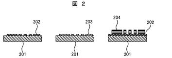
- FIG. 6 illustrates a cross section of a photomask.
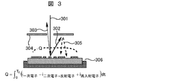
- the figure explaining the principle of sample charge based on electron beam irradiation.
- the figure which shows the example of the dimension change by charge accumulation
- a circuit pattern on a wafer is mainly formed by a technique of transferring an opaque film pattern formed on a transparent substrate called a photomask using a short wavelength ultraviolet laser beam having a wavelength of about 200 nm. Pattern dimension measurement is also an important quality control process.
- the photomask has a UV transmittance such as chromium 202 or molybdenum / silicon oxide (MoSiO) 203 on a substrate 201 made of a material having a high transmittance in the UV region such as synthetic quartz glass.
- a circuit pattern is formed of a low material.
- the photoresist 204 may exist on the chromium 202 or the molybdenum / silicon oxide (MoSiO) 203.
- MoSiO molybdenum / silicon oxide
- charge may be formed on the sample surface.
- quartz glass is the mainstream of the photomask substrate and is a dielectric, so in an electron microscope, the surface is charged by the action of the irradiated primary electron beam.
- an electric field is applied from the outside, it is easily polarized and generates a potential.
- the local electric field due to the generated electric charge affects the trajectory of the primary electron beam (electron beam), and may affect the observation image distortion, image movement, magnification change, and the like.
- a process for accumulating the charge on the sample was examined.
- the phenomenon when the sample is irradiated with the primary electron beam is shown in FIG.
- the primary electron beam 301 incident on the sample surface is reflected in the incident direction by so-called Rutherford scattering in the process of scattering in the sample constituent material (back scattered electrons 302), or the electrons in the shell are knocked out from the atoms and the secondary electrons are emitted.
- 303 is generated.
- the generation efficiency of secondary electrons (average number of secondary electrons generated from one primary electron) is determined by the composition of the material and is a function of the kinetic energy of the primary electrons.
- the generation efficiency (amount of electrons emitted from the sample / amount of electrons incident on the sample) exceeds 1.0, so that the sample is gradually positively charged.
- some of the primary electrons reflected backward may enter a nearby object such as the counter plate 304 and generate secondary electrons 305 again.
- This secondary electron re-enters the sample with energy of several electron volts (eV) and contributes to sample charging. That is, the charge accumulated in the sample per unit time is represented by the following relational expression (1). (For convenience, the polarity of the current by the electron beam is expressed as positive.)
- Equation (1) is close to 0, that is, the three currents appearing in Equation (1) are balanced. In order to reduce Q, it is desirable that the three currents are balanced immediately after the start of irradiation with the primary electron beam.
- the i primary electrons are set together with the incident energy of the primary electron beam by optimizing the image observation conditions.
- i secondary electrons + backscattered electrons are a function of the incident energy of the sample constituent material and the primary electron beam, and can be adjusted by optimizing the incident energy.
- the incident energy is determined by the voltage (retarding potential) applied to the holder 306 shown in FIG.
- i re-incident electrons are determined by the amount of secondary electrons and reflected electrons reaching the sample, and can be controlled by forming an appropriate electric field on the sample.
- Q can be reduced by optimizing the combination of the voltages applied to the holder 306 and the counter plate 304.
- a method of estimating the time variation of the inflow current to the sample and the charge amount of the sample by calculating the trajectory of the secondary electrons and the reflected electrons using the applied voltage as an initial condition can be considered.
- the main feature is also to easily switch the optimum potential setting for each sample.
- FIG. 1 is a schematic configuration diagram of a scanning electron microscope.
- a primary electron beam 101 emitted from an electron gun (not shown in the figure) located at the top of FIG. 1 is converged by a condenser lens 102 and deflected by a deflection coil 103, and finally has a diameter of several nm by an objective lens 104.
- the light is converged to an electron beam of (nanometer) and incident on the surface of the sample 105 to be observed. Some of the incident primary electrons are reflected back to become reflected electrons 106 (backscattered electrons). In addition, some of them generate secondary electrons 107 while being scattered in the sample.
- Secondary electrons are pulled upward by an electrostatic field formed between the sample 105 and the objective lens 104, collide with the conversion electrode 108, generate new secondary electrons, and are taken into the detector 109.
- the detector 109 has a built-in photomultiplier tube, which generates a voltage corresponding to the amount of secondary electrons, and after processing this by the signal processing device 110, displays it as an image on the image display unit 111.
- the sample 105 loaded on the holder 121 is placed on the precision stage 122. In order to observe a desired location on the sample, the observation location can be positioned directly below the axis of the electron optical system.
- the apparatus of this embodiment has a built-in power supply that applies a positive or negative voltage to the facing electrode and a negative voltage (retarding voltage) to the holder 121 or the precision stage 122.
- the retarding voltage is applied to decelerate the energy of the electron beam that reaches the sample.
- the configuration in which the holder 121 is arranged on the precision stage 122 is described.
- the present invention is not limited to this, and a holder-less configuration can be realized by providing a sample holding device on the precision stage 122. good.
- various sample support mechanisms are collectively referred to as a sample stage.
- a voltage or a current is applied or supplied to these electrodes and coils by a control device (not shown).
- the control device includes an arithmetic device, and the arithmetic device controls the device based on a scanning electron microscope operation program called a recipe. Further, the control device performs control as described later by reading the recipe from a storage medium (not shown).
- the signal processing device 110 forms a profile waveform with the vertical axis representing the signal amount and the horizontal axis representing the beam scanning position based on secondary electrons emitted from the sample. Then, the pattern dimension is measured by obtaining the distance between the peaks of the profile waveform.
- FIG. 4 is a diagram showing an example of the result of repeated measurement at the same point, which was executed under a certain potential condition A.
- FIG. 4 a 2 ⁇ m pitch pattern of the same line and space pattern equally arranged at 20 locations in the sample surface is sequentially measured, and this is repeated 20 cycles.
- the horizontal axis in FIG. 4 is the number of measurement points, and the vertical axis in the figure is a difference value from the first measurement value.
- This example shows a tendency that the dimension value 401 decreases in the order of measurement. This is because the effective magnification of the electron microscope changes as a result of the electric potential accumulated on the sample gradually changing the potential of the sample surface and affecting the trajectory of the primary electron beam.
- FIG. 402 is a curve obtained by calculating the fluctuation of the surface potential from the measurement result.
- the surface potential tends to rise relatively rapidly in the first half of the measurement and gradually saturate in the second half. Since the amount of charge of the sample does not change with time at the saturation point, the three currents of the formula (1) are balanced under the combined conditions of the sample surface potential and the counter plate set potential at the saturation point. Will be.
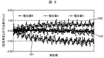
- FIG. 5 is a diagram illustrating a result of measurement equivalent to that in FIG. 4 under setting conditions A, B, and C in which the combination conditions of the voltage applied to the counter plate 115 and the retarding voltage are different.
- the setting condition A the dimensional value tends to decrease as in 501
- the result 502 of the setting condition C shows a slight upward tendency.
- the result 503 of the setting condition B has less variation in the measurement result due to the increase in the number of measurement points than the other setting conditions. Therefore, if the setting conditions A and C are initial conditions, if these conditions are brought close to the setting condition B, the magnification fluctuation based on the accumulation of cumulative charge can be suppressed even when measuring many points. can do.
- linear approximation it is effective to divide the horizontal axis into several sections, find a linear approximation formula in the section, and obtain the average value of the obtained slopes.
- quadratic approximation the average value up to the saturation point of the obtained approximate expression (the value obtained by dividing the integration value up to the saturation point by the integration interval) is calculated.
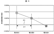
- Fig. 6 shows the correlation with the sample surface potential in the case of first-order approximation.
- the vertical axis represents the slope of the approximate expression.
- Reference numeral 503 in FIG. 5 is a repeated measurement result when the obtained potential condition B is set. As expected, there was no dimensional variation tendency, and the reproducibility of measurement was 0.6 nm or less, which could be suppressed to 0.03% when converted to magnification.
- the combination of the voltage applied to the facing electrode and the retarding voltage may be set so that the amount of electrons incident on the sample and the amount of electrons emitted from the sample are equal to each other. Therefore, one or both of the voltage applied to the facing electrode and the retarding voltage may be adjusted. However, if the retarding voltage is changed, the arrival energy of the beam that reaches the sample also changes. Therefore, from the viewpoint of not changing the arrival energy, it is preferable to selectively adjust the voltage applied to the facing electrode.
- the facing electrode may have a flat plate shape as illustrated in FIG. 1 or a cylindrical shape that covers the electron beam trajectory.
- FIG. 8 is a flowchart showing a measurement process for finding a combination condition of a voltage applied to the facing electrode and the retarding voltage.
- measurement conditions are set.
- the number of combinations of the facing electrode and the retarding voltage, the applied voltage, the number of measurement points, the measurement position, other optical conditions of the scanning electron microscope, and the like are set.
- the measurement position is determined based on the interval between measurement points where the influence of charging will be accumulated cumulatively.
- step 802 actual measurement is performed based on the setting conditions in step 801. Then, for the combination of one facing electrode and the retarding voltage, measurement is performed under the same setting conditions until the measurement for the set number of measurement points is completed (step 804). Then, it is determined whether or not the measurement for the set combination of the facing electrode and the retarding voltage has been completed (step 805). If the measurement has been completed, the inclination illustrated in FIG. 5 is calculated for each combination (step 806). . The calculation of the inclination may be performed when the measurement of each combination is completed.
- a graph as illustrated in FIG. 6 is created, and a combination having a slope of zero or close to zero is derived (step 807).
- the potential value at the intersection of the straight line (or curve) and zero slope may be obtained, but the device is limited to a predetermined applied voltage. If it cannot be set, a settable potential difference closest to the intersection may be used as the apparatus condition.
- a predetermined threshold value may be provided around the zero slope value, and a potential difference corresponding to the slope included in the threshold value may be set as the apparatus condition.
- the conditions obtained as described above are set as apparatus conditions (step 808).
- the device condition is set by adding and / or subtracting ⁇ V to the facing electrode and / or the retarding voltage.
- the flowchart of FIG. 7 is also a flowchart for explaining a process for setting the apparatus condition based on the tilt information.
- the S curve is a curve showing the relationship between the amount of electrons obtained when the energy filter is swept and the voltage applied to the energy filter, and the yield of secondary electrons from the sample is represented by the conversion electrode 108 in FIG.
- the voltage applied to the mesh electrode 123 placed below is recorded while running.
- the surface potential can be estimated from the change in the signal amount of secondary electrons with respect to the applied voltage (so-called S curve).
- the method for determining the application to the facing electrode and the retarding voltage by actually measuring the surface potential is shown in FIG.
- the optimized measurement potential condition can be registered in advance in the control device inside the apparatus. Called when setting measurement conditions, it is also possible to automatically switch potential conditions.
- the photomask has been described as an example of the measurement object by the SEM.
- the present invention is not limited to this. If the charging fluctuation in multipoint measurement is significant, the measurement condition setting of the semiconductor wafer is set. It is also possible to apply to.
Landscapes
- Chemical & Material Sciences (AREA)
- Analytical Chemistry (AREA)
- Length-Measuring Devices Using Wave Or Particle Radiation (AREA)
- Testing Or Measuring Of Semiconductors Or The Like (AREA)
Abstract
本発明は、測定点や検査点が多数存在する場合であっても、帯電の影響に基づく、測定,検査精度の低下を抑制し得る光学条件の設定を可能とする荷電粒子線装置の光学条件設定方法、及び荷電粒子線装置の提供を目的とする。 上記目的を達成するために、電子線で試料表面を走査することによって試料から放出される電子の検出に基づいて、前記試料上のパターンを測定する走査電子顕微鏡、或いは光学条件設定方法であって、試料上の複数の測定点の測定値から、測定数に対する測定値の変化を求め、当該変化の傾斜がゼロ、或いはゼロに近くなるように、試料表面電界を制御する走査電子顕微鏡、或いは光学条件設定方法を提案する。
Description
本発明は、走査電子顕微鏡の光学条件調整方法、及び走査電子顕微鏡に係り、特に帯電する試料であっても適正に光学条件を設定し得る方法、及び装置に関する。
試料表面の分析装置として、表面を荷電粒子線プローブで走査し、放出される二次電子,イオン,電磁波などの信号の量ないしエネルギーを解析して表面性状を分析するものは、表面の微細形状,構成元素等に関する情報を用意に得られる利点がある。特にプローブとして電子を、放出信号として二次電子を用い、二次電子量を画面上の輝度に変換して表面形状像を得る走査電子顕微鏡(SEM:Scanning Electron Microscope)は広く実用に供されている。また、半導体素子の検査装置として、走査電子顕微鏡から派生した寸法検査装置である測長SEM(Critical Dimension-SEM:CD-SEM)や、形状検査装置である検査SEMなどが半導体製造産業で広く用いられている。
走査電子顕微鏡に代表される荷電粒子線装置は、電荷を持つビームを試料に照射する装置であるため、試料が帯電する可能性がある。試料に付着した帯電は、荷電粒子ビームに影響を与え、荷電粒子ビームの光学条件を変化させてしまう可能性があるため、帯電の正確な検出や、適正な光学条件調整が求められる。
特許文献1には、複数の測定位置にて、エネルギフィルタを用いた表面電位の測定を行うことで、試料全体に亘って蓄積する大域帯電を測定する手法が説明されている。特許文献2にも、エネルギフィルタを用いた帯電測定法や、設定倍率に応じて帯電量を計算によって求める手法が提案されている。
特許文献3には、荷電粒子線装置のチャージアップ防止法が説明されており、試料(ターゲット)に印加する電圧を変化させ、その都度、電子線で絶縁性ターゲット上に存在する直線部を有する個所を走査し、当該走査により発生した二次電子信号を微分した信号のピークの内、最も大きいピーク値が発生した時の印加電圧値を、ターゲットに印加することで、絶縁性ターゲットのチャージアップを無くす手法が説明されている。また、引用文献4にも同様に、ビームエネルギーを変化させることで得られる複数のスコアを解析することで、試料に蓄積する帯電によるフォーカスずれを補償する手法が説明されている。
近年、半導体検査や測定に用いられる走査電子顕微鏡(Scanning Electron Microscope:SEM)の検査,測定点数は増加の一途を辿っている。例えば、半導体パターンやフラットパネル等の転写に用いられるフォトマスクでは、パターン等の微細化に伴い、光近接効果(Optical Proximity Correction:OPC)の影響によって設計データに忠実なレジストパターンを形成することが困難になりつつある。このような課題に対し、補助パターン(OPCパターン)を付加することによって、適正なパターン形成を実現する試みがなされている。このようなOPCパターンは、半導体素子の高集積化,微細化に伴い、複雑となり、その結果、走査電子顕微鏡による検査,測定点も増大傾向にある。
一方、測定点の増加に伴い、帯電が累積的に蓄積する現象が認められるようになってきた。試料に入射する電子数と、試料から放出される電子数が等しくないと、試料は正か負に帯電する。特に上述のように、試料上に多数の測定点が存在すると、個々の帯電が累積され、試料表面の電位を変化させることになる。
特許文献1,2に説明されているようなエネルギフィルタによる帯電測定法によれば、走査電子顕微鏡の視野(Field Of View:FOV)の帯電を正確に測定することができるが、上述のような累積的に蓄積される帯電については、何も言及されていない。また、特許文献3,4のように、試料に付着する帯電を相殺するように、試料への印加電圧を調整する手法では、徐々に蓄積される帯電に追従するように、光学条件を調整する必要があり、多点測定時のスループットを低下させてしまい、且つ倍率変動等に対応することができない。
以下に、測定点や検査点が多数存在する場合であっても、帯電の影響に基づく、測定,検査精度の低下を抑制し得る光学条件の設定を目的とする荷電粒子線装置の光学条件設定方法、及び荷電粒子線装置について説明する。
上記目的を達成するための一態様として、電子線で試料表面を走査することによって試料から放出される電子の検出に基づいて、前記試料上のパターンを測定する走査電子顕微鏡、或いは光学条件設定方法であって、試料上の複数の測定点の測定値から、測定数に対する測定値の変化を求め、当該変化の傾斜がゼロ、或いはゼロに近くなるように、試料表面電界を制御する走査電子顕微鏡、或いは光学条件設定方法を提案する。
上記構成によれば、試料上に存在する複数の測定,検査点への電子線照射に基づく累積的な帯電の蓄積の影響を抑制し、高精度な測定や検査を実現することが可能となる。
ウェーハ上の回路パターンの形成は、フォトマスクと呼ばれる透明基板上に形成された不透明膜のパターンを波長200nm程度の短波長紫外線レーザ光などを用いて転写する技術が主流であり、フォトマスク上のパターンの寸法測定も重要な品質管理工程である。フォトマスクは、図2に示すように、合成石英ガラスなど紫外線領域の透過率が高い材質で作られた基板201上に、クロム202、ないしモリブデン・珪素酸化物(MoSiO)203など紫外線透過率の低い材質により回路パターンを形成したものである。
また、マスク製作過程では、クロム202ないしモリブデン・珪素酸化物(MoSiO)203上にフォトレジスト204が存在することもある。このようなフォトマスクを走査電子顕微鏡で観察する場合、試料表面に帯電が形成されることがある。フォトマスクの基板は前述のように石英ガラスが主流であり、誘電体なので、電子顕微鏡においては、照射される一次電子線の作用で表面が帯電する。また、外部から電場を印加することにより容易に分極し電位を生ずる。発生した電荷による局所的な電場は、一次電子線(電子ビーム)の軌道に影響を与え、観察像の歪み,像の移動,倍率の変化などの影響を及ぼすことがある。
これまで、試料への影響を緩和するために、一次電子線の入射エネルギー(加速電圧)を低くし、電子線電流(プローブ電流)を減らすという試みが行われてきたが、フォトマスクのように試料体積のほとんどが誘電体で構成される場合には、上述のような帯電の影響を充分に抑制することが困難である。また、観察する試料表面近傍の空間に不活性気体分子を適当な分圧で存在させ、一次電子線の作用で弱電離した分子により積極的に基板表面の電荷を除去するという技術も実用化されている。しかしこの場合、不活性分子が二次電子を散乱するため、画像信号が劣化するという問題があり、半導体製造業では普及するに到っていない。さらに、試料に対して別途生成した荷電粒子を照射するという技術も提案されているが、試料帯電の中和点を適切に定めるのが困難であり、実用化されていない。
そこで本実施例においては、試料への帯電の蓄積のプロセスを検討した。試料に一次電子線が照射されたときの現象を図3に示す。試料表面に入射した一次電子線301は、試料構成物質内を散乱する過程で、いわゆるラザフォード散乱により入射方向へ反射する(後方散乱電子302)か、あるいは、原子から殻内電子をたたき出し二次電子303を生成する。二次電子の生成効率(一個の一次電子から平均何個の二次電子が生成するか)は物質の組成により定まり、一次電子の運動エネルギーの関数である。一般的に、走査電子顕微鏡で用いられるエネルギー領域においては、生成効率(試料から放出される電子量/試料に入射する電子量)は1.0を越えるため、試料は徐々に正に帯電する。しかし、後方に反射した一次電子の一部は、対向板304など近傍の物体に入射し、再度二次電子305を発生させることがある。
この二次電子は数電子ボルト(eV)のエネルギーで試料に再入射し、試料帯電に寄与する。すなわち単位時間に試料に蓄積される電荷は以下の関係式(1)で表される。(便宜的に電子線による電流の極性を正で表した。)

いま、Qをなるべく小さくすることを考える。これは、式(1)における被積分関数が0にちかくなること、すなわち、式(1)に現れる3つの電流が平衡することを意味する。Qを小さくするためには、一次電子線の照射開始直後から、上記3つの電流が平衡していることが望ましい。
i一次電子は像観察条件の最適化によって一次電子線の入射エネルギーと共に設定される。i二次電子+反射電子は、試料構成物質と一次電子線の入射エネルギーの関数であり、入射エネルギーの最適化により調整することができる。
入射エネルギーは、図3に示すホルダー306に印加される電圧(リターディング電位)で決定される。一方、i再入射電子は、試料への二次電子や反射電子の到達量で決定されるので、これを制御するには、試料上に適当な電界を形成することで制御することができる。
したがって、ホルダー306及び対向板304にかける電圧の組み合わせで最適化することによりQを低減することが可能である。これらの組み合わせを検討するにあたり、印加電圧を初期条件として二次電子および反射電子の軌道計算を行い、試料への流入電流等および試料の帯電量の時間変化を推定する方法も考えられる。しかし、実際には計算だけで最適な印加電圧の組み合わせを推定するのは種々の要因によって困難であることが多い。
本実施例では、軌道計算ではなく、個々の材質の試料に対しいくつかの電位条件で繰り返し測定を行い、その結果から、試料の帯電量を最小にするための電位条件を求める方法、およびそのような手段を備えた走査電子顕微鏡を提供するものである。なお、以下に説明する手法は、フォトマスク観察のように、試料の構成材料が業界内で標準化されていて、少数の特定材料に限定されている場合に、きわめて有効である。
特に、近年の半導体素子の高集積化,微細化にともない、計測への精度も厳しく要求されると共に、OPCパターンの複雑化により、測定点数も何千点にまで及ぶ場合がある。SEMによる測定等を実行している間に、微小な帯電が蓄積することによる倍率変動が発生することが考えられる。以下に説明する光学条件設定方法は、測定の高精度化を実現する上で、極めて有効な手段となり得る。
本実施例では、主に試料を走査電子顕微鏡で観察する際に、試料帯電蓄積の影響により倍率変動が発生するという技術課題を解決するための手法を説明する。
そのための解決手段として、試料に蓄積される電荷を減らすために、実多点測定結果から試料帯電の中和点となる最適な電位を求め、評価装置に設定する手法を提案する。また試料毎に最適な電位設定を簡易に切換えることも主要な特徴とする。
上記手法によれば、試料の構成材料ごとに帯電蓄積を抑制し、多点測定における倍率変動を計測誤差範囲以内に抑えられるため、高精度の多点測定が可能となる。あらかじめ構成材料が判っている数種の試料に観察対象が限られている場合は、きわめて有効である。
図1は、走査電子顕微鏡の概略構成図である。図1の上方にある電子銃(本図では省略)から射出された一次電子線101は、コンデンサレンズ102で収束され、偏向コイル103で偏向された後、対物レンズ104で最終的に径数nm(ナノメートル)の電子線に収束されて、観察対象である試料105の表面に入射する。入射した一次電子の一部は後方反射し、反射電子106(後方散乱電子)となる。また一部は試料内を散乱しながら二次電子107を生成する。
二次電子は試料105と対物レンズ104との間に形成される静電場により上方に引き上げられ、変換電極108と衝突し、新たな二次電子を発生し、検出器109に取り込まれる。検出器109には光電子倍増管が内蔵されており、二次電子の量に応じた電圧を発生させるので、これを信号処理装置110で処理した後、画像表示部111にて画像として表示する。ホルダー121にロードされた試料105は精密ステージ122の上に載置されており、試料上の所望の場所を観察するために、電子光学系の軸直下に観察箇所を位置させることができる。ホルダー121及び対向板115(対面電極)にかける電圧の組み合わせで最適化することにより多点測定の帯電蓄積を抑制することが可能である。
本実施例装置は、対面電極に正或いは負の電圧を、ホルダー121或いは精密ステージ122に負の電圧(リターディング電圧)を印加するような電源が内蔵されている。リターディング電圧は、試料に到達する電子ビームのエネルギーを減速するために印加されるものである。本実施例では、精密ステージ122上にホルダー121を配置する構成を説明しているが、これに限られることはなく、精密ステージ122に試料保持装置を設けることにより、ホルダレスとするようにしても良い。本明細書では、種々の試料支持機構を包括して試料台と称する。
なお、これらの電極やコイルには、図示しない制御装置によって、電圧、或いは電流が印加或いは供給される。制御装置は、演算装置を備えてなり、当該演算装置は、レシピと呼ばれる走査電子顕微鏡の動作プログラムに基づいて、装置を制御する。また、制御装置は図示しない記憶媒体から、上記レシピを読み出すことによって、後述するような制御を行う。また、信号処理装置110は、試料から放出される二次電子等に基づいて、縦軸を信号量、横軸をビームの走査位置とするプロファイル波形を形成する。そして当該プロファイル波形のピーク間の距離を求めることによって、パターン寸法を測定するように動作する。
図4は、ある電位条件Aにて実行された、同一点の繰り返し測定の結果一例を示す図である。図4は、試料面内の20箇所に均等に配置された同一ラインアンドスペースパターンの2μmのピッチパターンを順次測定し、これを20周期繰り返す。図4の横軸は、測定点数であり、図の縦軸は、1回目の測定値からの差分値である。この例は、測定順に、寸法値401が減少していく傾向を示している。これは、試料に蓄積された電荷により試料表面の電位が徐々に変化し、一次電子線の軌道に影響を及ぼす結果、電子顕微鏡の実効倍率が変化するためである。
同図402は、測定結果から表面電位の変動を算出した曲線である。表面電位は、測定の前半部は比較的に急に上昇し、後半部は緩やかに飽和していく傾向を示す。飽和点においては試料の帯電量が時間的に変化していないのであるから、飽和点における試料表面電位および対向板設定電位の組み合わせ条件下で、式(1)の3種の電流が平衡していることになる。
したがって、このときの試料表面電位を知れば、帯電の蓄積による倍率変動が抑制できることが可能である。このことを踏まえ、本実施例では、以下の手法を提案する。図5は、対向板115に印加する電圧と、リターディング電圧との組み合わせ条件が異なる設定条件A,B,Cにて、図4と同等の測定を行った結果を示す図である。設定条件Aでは、501のように、寸法値が減少する傾向を示すのに対し、設定条件Cの結果502は、逆に僅かな上昇傾向を示した。この図からみて判る通り、設定条件Bの結果503は、その他の設定条件と比べると、測定点数の増加に伴う測定結果の変動が少ない。よって、設定条件AやCが初期条件であるならば、これらの条件を設定条件Bに近づけるようにすれば、多数点の測定の際にも、累積的な帯電の蓄積に基づく倍率変動を抑制することができる。
図5の測長値変化曲線をそれぞれ一次直線ないし二次曲線で多項式近似し、係数を算出する。一次近似の場合は、横軸をいくつかの区間に分け、区間内の直線近似式を求め、得られた傾きの平均値を求める方法が有効である。二次近似の場合は、得られた近似式の飽和点までの平均値(飽和点までの積分値を積分区間で除したもの)を算出する。
一次近似の場合の、試料表面電位との相関を図6に示す。縦軸は近似式の傾きである。傾きの0点が得られる電圧条件Bにおいて、試料表面電位の時間変化が最小となり、表面帯電がほぼ0となると考えられる。図5の503は、得られた電位条件Bを設定した場合の繰り返し測定結果である。予想通り、寸法変動の傾向がなく、測定の繰り返し再現性を0.6nm以下、倍率に換算すると0.03%以内に抑えることができた。
なお、対面電極とリターディング電圧に印加する電圧の組み合わせは、試料へ入射する電子量と、試料から放出される電子量が、等しくなるように設定されれば良く、その関係は試料表面の電界によって決定されるため、対面電極への印加電圧とリターディング電圧の一方、或いは両方を調整対象とするようにしても良い。但し、リターディング電圧を変えると、試料に到達するビームの到達エネルギーも変化することになるので、到達エネルギーを変化させないという観点から見れば、対面電極への印加電圧を選択的に調整すると良い。また、対面電極は、図1に例示するような平板形状のものでも良いし、電子ビーム軌道を覆うような筒形状のものでも良い。
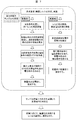
図8は対面電極とリターディング電圧に印加する電圧の組み合わせ条件を見出すための測定プロセスを示すフローチャートである。まず、ステップ801にて測定条件を設定する。ここでは、対面電極とリターディング電圧の組み合わせの数,印加電圧,測定点数,測定位置,走査電子顕微鏡の他の光学条件等が設定される。測定位置は帯電の影響が累積的に蓄積されるであろう測定点間間隔に基づいて決定する。
次に、ステップ802にて、ステップ801での設定条件に基づいて、実際の測定を行う。そして1つの対面電極とリターディング電圧の組み合わせについて、設定された測定点数分の測定が終了するまで、同じ設定条件にて測定を行う(ステップ804)。そして、設定された対面電極とリターディング電圧の組み合わせ分の測定が終了したかを判断(ステップ805)し、終了した場合には、組み合わせ毎に図5に例示した傾きを算出する(ステップ806)。なお、傾きの算出は、各組み合わせの測定が終了した時点で行うようにしても良い。
そして、複数の傾き情報と組み合わせ情報に基づいて、図6に例示したようなグラフを作成し、傾きがゼロ、或いはゼロに近い組み合わせを導出する(ステップ807)。この場合、直線(或いは曲線)と傾きゼロの交点の電位値(リターディング電圧と対面電極への印加電圧との電位差)を求めるようにすれば良いが、装置が限られた所定の印加電圧しか設定し得ないものであるならば、上記交点に最も近い設定可能な電位差を装置条件とするようにしても良い。また、傾きゼロ値を中心として、所定の閾値を設けておき、当該閾値内に含まれる傾きに対応する電位差を装置条件として設定するようにしても良い。
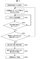
以上のようにして求められた条件を装置条件として設定する(ステップ808)。例えば図6の電位値Cが初期の装置条件であったとすれば、対面電極及び/又はリターディング電圧にΔVを加算及び/又は減算することによって、装置条件の設定を行う。図7のフローチャートも傾き情報に基づいて、装置条件を設定するための工程を説明するフローチャートである。求められた計測条件を、試料の種類毎にレシピとして記憶することによって、同じ試料、或いは同じ材質の試料を測定するときに、予め作成されたレシピを読み出して設定することが可能となる。
測定値が飽和した状態で、直接表面電位を計測し、試料への電流が平衡する電位を求めることも可能である。具体的には、図4と同様に寸法を測定する際、測定開始前および測定値の飽和後に、それぞれ表面電位を測定し、表面電位の変化値405ΔV=VA′-VAを算出する。
真空中の表面電位計測手法としては、エネルギフィルタを用いてSカーブを作成する手法がある。Sカーブは、エネルギフィルタを掃印したときに得られる電子量と、エネルギフィルタへの印加電圧との関係を示す曲線であり、試料からの二次電子の収量を、図1の変換電極108の下におかれたメッシュ電極123に印加した電圧を走引しながら記録する。印加電圧に対する二次電子の信号量変化(いわゆるSカーブ)から表面電位を推定することができる。表面電位を実際に測定することによって、対面電極への印加やリターディング電圧を決定する手法についても、実施例1と同様に、フローチャートを図7に示した。
上記いずれの実施例においても、最適化された計測の電位条件は、予め装置内部の制御装置に、登録しておくことができる。計測条件を設定する際に呼び出し、電位条件を自動的に切り替えることも可能である。
なお、上述の実施例では、SEMによる測定対象として、フォトマスクを例に説明したが、これに限られることはなく、多点測定における帯電変動が顕著であるならば、半導体ウェーハの測定条件設定に適用することも可能である。
101 一次電子線
102 コンデンサレンズ
103 偏向コイル
104 対物レンズ
105 試料
106 反射電子
107 二次電子
108 変換電極
109 検出器
110 信号処理装置
111 画像表示部
115 対向板
102 コンデンサレンズ
103 偏向コイル
104 対物レンズ
105 試料
106 反射電子
107 二次電子
108 変換電極
109 検出器
110 信号処理装置
111 画像表示部
115 対向板
Claims (5)
- 電子線で試料表面を走査することによって試料から放出される電子の検出に基づいて、前記試料上のパターンを測定する走査電子顕微鏡であって、
前記試料に到達する電子線を減速するための負電圧が印加される試料台と、前記試料上で発生する電界を制御する対面電極を備え、
前記試料上の複数の測定点の測定値から、測定数に対する測定値の変化を求め、当該変化の傾斜がゼロ、或いはゼロに近くなるような試料台への印加電圧、及び/又は対面電極への印加電圧を演算する演算装置を備えたことを特徴とする走査電子顕微鏡。 - 請求項1において、
前記演算装置は、前記試料台と対面電極との間の電位差毎に、複数の測定点に対する測定値の変化を求め、当該電位差毎に求められる測定値の変化の傾きに基づいて、当該傾きがゼロ、或いはゼロに近くなるような前記電位差を算出することを特徴とする走査電子顕微鏡。 - 請求項1において、
前記試料から放出される電子のエネルギー分析を行うエネルギフィルタを備え、
前記演算装置は、前記試料に対する測定開始前の試料表面電位と、前記複数の測定を実施することによって、試料表面電位の上昇が飽和したときの試料表面電位との電位差を算出することを特徴とする走査電子顕微鏡。 - 請求項1において、
前記演算装置は、前記試料の材質に応じて、試料台への印加電圧、及び/又は対面電極への印加電圧を設定することを特徴とする走査電子顕微鏡。 - 走査電子顕微鏡を用いて、電子線で試料表面を走査することによって試料から放出される電子の検出に基づいて、前記試料上のパターンを測定する走査電子顕微鏡の光学条件設定方法において、
前記試料上の複数の測定点の測定値から、測定数に対する測定値の変化を求め、当該変化の傾斜がゼロ、或いはゼロに近くなるように、前記試料表面電界を制御することを特徴とする走査電子顕微鏡の光学条件設定方法。
Priority Applications (1)
| Application Number | Priority Date | Filing Date | Title |
|---|---|---|---|
| US13/578,179 US8692197B2 (en) | 2010-02-26 | 2011-02-09 | Scanning electron microscope optical condition setting method and scanning electron microscope |
Applications Claiming Priority (2)
| Application Number | Priority Date | Filing Date | Title |
|---|---|---|---|
| JP2010041238A JP5624774B2 (ja) | 2010-02-26 | 2010-02-26 | 走査電子顕微鏡の光学条件設定方法、及び走査電子顕微鏡 |
| JP2010-041238 | 2010-02-26 |
Publications (1)
| Publication Number | Publication Date |
|---|---|
| WO2011105015A1 true WO2011105015A1 (ja) | 2011-09-01 |
Family
ID=44506450
Family Applications (1)
| Application Number | Title | Priority Date | Filing Date |
|---|---|---|---|
| PCT/JP2011/000704 Ceased WO2011105015A1 (ja) | 2010-02-26 | 2011-02-09 | 走査電子顕微鏡の光学条件設定方法、及び走査電子顕微鏡 |
Country Status (3)
| Country | Link |
|---|---|
| US (1) | US8692197B2 (ja) |
| JP (1) | JP5624774B2 (ja) |
| WO (1) | WO2011105015A1 (ja) |
Cited By (1)
| Publication number | Priority date | Publication date | Assignee | Title |
|---|---|---|---|---|
| CN104798172A (zh) * | 2012-11-26 | 2015-07-22 | 株式会社日立高新技术 | 试样台、带电粒子束装置及试样观察方法 |
Families Citing this family (1)
| Publication number | Priority date | Publication date | Assignee | Title |
|---|---|---|---|---|
| JP5764444B2 (ja) * | 2011-09-16 | 2015-08-19 | 株式会社日立ハイテクノロジーズ | 走査電子顕微鏡 |
Citations (1)
| Publication number | Priority date | Publication date | Assignee | Title |
|---|---|---|---|---|
| JP2005345272A (ja) * | 2004-06-03 | 2005-12-15 | Hitachi High-Technologies Corp | 試料像取得方法及び走査電子顕微鏡 |
Family Cites Families (13)
| Publication number | Priority date | Publication date | Assignee | Title |
|---|---|---|---|---|
| JP2607652B2 (ja) * | 1988-12-12 | 1997-05-07 | 日本電信電話株式会社 | 荷電ビームを用いた測定装置における照射条件決定方法およびそれに用いる評価パタン |
| JPH04229541A (ja) | 1990-12-26 | 1992-08-19 | Jeol Ltd | 荷電粒子線装置におけるチャージアップ防止装置 |
| US6521891B1 (en) | 1999-09-03 | 2003-02-18 | Applied Materials, Inc. | Focusing method and system |
| JP4015352B2 (ja) * | 2000-02-22 | 2007-11-28 | 株式会社日立製作所 | 荷電粒子ビームを用いた検査方法 |
| WO2003007330A1 (fr) | 2001-07-12 | 2003-01-23 | Hitachi, Ltd. | Procede de mesure de l'electrisation d'un echantillon et dispositif a faisceau de particules chargees |
| JP3955450B2 (ja) * | 2001-09-27 | 2007-08-08 | 株式会社ルネサステクノロジ | 試料検査方法 |
| JP4895569B2 (ja) * | 2005-01-26 | 2012-03-14 | 株式会社日立ハイテクノロジーズ | 帯電制御装置及び帯電制御装置を備えた計測装置 |
| JP4644617B2 (ja) * | 2006-03-23 | 2011-03-02 | 株式会社日立ハイテクノロジーズ | 荷電粒子線装置 |
| JP4795883B2 (ja) * | 2006-07-21 | 2011-10-19 | 株式会社日立ハイテクノロジーズ | パターン検査・計測装置 |
| US7612570B2 (en) * | 2006-08-30 | 2009-11-03 | Ricoh Company, Limited | Surface-potential distribution measuring apparatus, image carrier, and image forming apparatus |
| JP5164355B2 (ja) * | 2006-09-27 | 2013-03-21 | 株式会社日立ハイテクノロジーズ | 荷電粒子ビームの走査方法及び荷電粒子線装置 |
| JP5075431B2 (ja) | 2007-02-28 | 2012-11-21 | 株式会社日立ハイテクノロジーズ | 帯電測定方法、焦点調整方法、及び走査電子顕微鏡 |
| JP4637195B2 (ja) * | 2008-03-05 | 2011-02-23 | 株式会社日立ハイテクノロジーズ | 試料の電位測定方法及び荷電粒子線装置 |
-
2010
- 2010-02-26 JP JP2010041238A patent/JP5624774B2/ja not_active Expired - Fee Related
-
2011
- 2011-02-09 US US13/578,179 patent/US8692197B2/en not_active Expired - Fee Related
- 2011-02-09 WO PCT/JP2011/000704 patent/WO2011105015A1/ja not_active Ceased
Patent Citations (1)
| Publication number | Priority date | Publication date | Assignee | Title |
|---|---|---|---|---|
| JP2005345272A (ja) * | 2004-06-03 | 2005-12-15 | Hitachi High-Technologies Corp | 試料像取得方法及び走査電子顕微鏡 |
Cited By (1)
| Publication number | Priority date | Publication date | Assignee | Title |
|---|---|---|---|---|
| CN104798172A (zh) * | 2012-11-26 | 2015-07-22 | 株式会社日立高新技术 | 试样台、带电粒子束装置及试样观察方法 |
Also Published As
| Publication number | Publication date |
|---|---|
| JP5624774B2 (ja) | 2014-11-12 |
| US8692197B2 (en) | 2014-04-08 |
| JP2011181188A (ja) | 2011-09-15 |
| US20120318977A1 (en) | 2012-12-20 |
Similar Documents
| Publication | Publication Date | Title |
|---|---|---|
| JP5941704B2 (ja) | パターン寸法測定装置、及びコンピュータプログラム | |
| US8816276B2 (en) | Electron beam writing apparatus and electron beam writing method | |
| US20110057101A1 (en) | Charged particle beam system | |
| US8481935B2 (en) | Scanning electron microscope | |
| US11133148B2 (en) | Scanning electron microscope | |
| US20070181808A1 (en) | Electron microscope and electron bean inspection system. | |
| TWI592976B (zh) | Charged particle beam device and inspection method using the device | |
| US9324540B2 (en) | Charged particle beam device | |
| US8907267B2 (en) | Charged particle beam device | |
| US20150262857A1 (en) | Electrostatic Chuck Mechanism and Charged Particle Beam Apparatus | |
| JP5094282B2 (ja) | ローカル帯電分布精密計測方法及び装置 | |
| WO2008029696A1 (en) | Electron beam dimension measuring device and electron beam dimension measuring method | |
| US8507857B2 (en) | Charged particle beam inspection apparatus and inspection method using charged particle beam | |
| JP5624774B2 (ja) | 走査電子顕微鏡の光学条件設定方法、及び走査電子顕微鏡 | |
| JP5277008B2 (ja) | パターン測定条件設定方法、及びパターン測定条件設定装置 | |
| JP4438439B2 (ja) | 表面電荷分布測定方法及び装置並びに、感光体静電潜像分布測定方法及びその装置 | |
| JP7294981B2 (ja) | 電子線装置及び電極 | |
| JP2015056376A (ja) | 走査透過電子顕微鏡及びその収差測定方法 | |
| TWI747269B (zh) | 帶電粒子束系統、及帶電粒子線裝置中的決定觀察條件之方法 | |
| JP5563801B2 (ja) | 荷電粒子ビーム分解能測定方法および荷電粒子ビーム描画装置 | |
| JP5349978B2 (ja) | 荷電粒子線を用いた寸法計測方法、および寸法計測装置 | |
| JP5531834B2 (ja) | 高抵抗体の帯電特性評価装置、帯電特性評価方法および帯電特性評価プログラム | |
| JP4906409B2 (ja) | 電子ビーム寸法測定装置及び電子ビーム寸法測定方法 | |
| JP2006344614A (ja) | 露光方法及び露光装置 | |
| JP2011228501A (ja) | 荷電粒子ビーム描画方法および荷電粒子ビーム描画装置 |
Legal Events
| Date | Code | Title | Description |
|---|---|---|---|
| 121 | Ep: the epo has been informed by wipo that ep was designated in this application |
Ref document number: 11746988 Country of ref document: EP Kind code of ref document: A1 |
|
| WWE | Wipo information: entry into national phase |
Ref document number: 13578179 Country of ref document: US |
|
| NENP | Non-entry into the national phase |
Ref country code: DE |
|
| 122 | Ep: pct application non-entry in european phase |
Ref document number: 11746988 Country of ref document: EP Kind code of ref document: A1 |