WO2011102584A1 - 신규의 금속 디알킬글리신 화합물 및 그 제조 방법 - Google Patents
신규의 금속 디알킬글리신 화합물 및 그 제조 방법 Download PDFInfo
- Publication number
- WO2011102584A1 WO2011102584A1 PCT/KR2010/006959 KR2010006959W WO2011102584A1 WO 2011102584 A1 WO2011102584 A1 WO 2011102584A1 KR 2010006959 W KR2010006959 W KR 2010006959W WO 2011102584 A1 WO2011102584 A1 WO 2011102584A1
- Authority
- WO
- WIPO (PCT)
- Prior art keywords
- indium
- gallium
- metal
- compound
- dialkylglycine
- Prior art date
- Legal status (The legal status is an assumption and is not a legal conclusion. Google has not performed a legal analysis and makes no representation as to the accuracy of the status listed.)
- Ceased
Links
Images






Classifications
-
- C—CHEMISTRY; METALLURGY
- C07—ORGANIC CHEMISTRY
- C07C—ACYCLIC OR CARBOCYCLIC COMPOUNDS
- C07C229/00—Compounds containing amino and carboxyl groups bound to the same carbon skeleton
- C07C229/02—Compounds containing amino and carboxyl groups bound to the same carbon skeleton having amino and carboxyl groups bound to acyclic carbon atoms of the same carbon skeleton
- C07C229/04—Compounds containing amino and carboxyl groups bound to the same carbon skeleton having amino and carboxyl groups bound to acyclic carbon atoms of the same carbon skeleton the carbon skeleton being acyclic and saturated
- C07C229/06—Compounds containing amino and carboxyl groups bound to the same carbon skeleton having amino and carboxyl groups bound to acyclic carbon atoms of the same carbon skeleton the carbon skeleton being acyclic and saturated having only one amino and one carboxyl group bound to the carbon skeleton
- C07C229/10—Compounds containing amino and carboxyl groups bound to the same carbon skeleton having amino and carboxyl groups bound to acyclic carbon atoms of the same carbon skeleton the carbon skeleton being acyclic and saturated having only one amino and one carboxyl group bound to the carbon skeleton the nitrogen atom of the amino group being further bound to acyclic carbon atoms or to carbon atoms of rings other than six-membered aromatic rings
Definitions
- the present invention relates to novel indium or gallium trivalent dialkylglycine compounds, and more particularly, to metal dialkylglycine compounds useful as precursors for the preparation of materials comprising indium or gallium and methods for their preparation.
- Indium is useful because of its high resistance to abrasion in electroplating and low resistance to contact with aluminum wires.Indium coating of sodium vapor lamp in Europe Indium oxide may be used as a material. Indium oxide and tin-indium oxide films are also used in conductive coating materials and electroluminescent pannels in glass and ceramics. Indium oxide can also be used as a heat insulator and in the solar cell or semiconductor industry (M. Veith, S. Hill, V. Huch, Eur. J. Inorg. Chem., 1999, 1343) . It can also be used for photoelectrode materials, liquid crystal displays, photovoltaic devices, etc. (CR Patra, A. Cyprus, New. J. Chem., 2004, 28, 1060 ).
- InCl 3 may have chlorine contamination in thin film deposition and requires an oxygen source from the outside, and trialkylindium (III) such as Me 3 In or Et 3 In is volatile. It is good but has the disadvantage of being very sensitive to oxygen and moisture (C. Xu, TH Baum, I. Guzei, AL Rheingold, Inorg. Chem., 2000, 39, 2008).
- Indium alkoxides such as [In (OC 2 H 4 OMe) 3 ] m and [In (OC 2 H 4 NMe 2 ) 3 ] m are known to be difficult to use because they are not volatile and unstable in air (S. Daniele, D. Tchebou, LG Hubert-Pfalzgraf, S. Lecocq, Inorg.Chem. Comm., 2002, 5, 347).
- Other precursors include betadike, such as In (thd) 3 (where thd is 2,2,6,6-tetramethyl-3,5-heptadionate) and In (acac) 3 (where acac is acetylacetonate) Compounds using tonate ligands (P.
- amino alkoxide strains are known to be more useful than alkoxy alkoxides (LG Hubert-Pfalzgraf, H. Guillon, Appl. Organomet. Chem., 1998, 12, 221).
- the precursor In general, in order to prepare a thin film by a vacuum process, the precursor must have high volatility, and to prepare a nanomaterial using a solution process, the precursor must be stable and easy to handle in air.
- indium compounds have been used in combination with other metals, such as transparent electronic devices such as indium-gallium-zinc oxide (IGZO) or copper indium gallium selenide (CIGS).
- IGZO indium-gallium-zinc oxide
- CIGS copper indium gallium selenide
- U. S. Patent No. 6,127, 202 synthesizes Cu-In-O, Cu- (In, Ga) -O (hereafter CI, CIG oxide) oxide precursors in the nanoparticle synthesis step, and then uses the same to prepare a CIS and CIGS light absorbing layer. Reported how to do it.
- Electrodeposition can simplify CIGS thin film production without additional processes such as precursor synthesis.
- Several techniques have also been proposed for CIGS thin film processes using electrodeposition.
- International Patent (PCT) WO01 / 078154 reports on the preparation of CIGS thin films by electrodeposition in solution.
- Gallium oxide (Ga 2 O 3 ) is attracting attention as a new material for gas sensors, transparent conductors, phosphors, etc., and as a wide band gap compound (4.8 eV) In the state where oxygen is slightly deficient by addition of another compound, it becomes an n-type semiconductor.
- Ga 2 O 3 is an electrical insulator at room temperature and a semiconductor at temperatures above 500 ° C. having a chemically and thermally stable monoclinic form. Above 900 ° C, since the electrical conductivity changes depending on the concentration of oxygen, the oxygen concentration can be detected. Below 900 ° C it acts as a surface-control-type sensor to reduce gases such as ethanol. Therefore, it can be used as a gas sensor according to temperature.
- Ga 2 O 3 : Mn, Ga 2 O 3 : Cr, Ga 2 O 3 : Eu is a high emission multicolor emission in a thin-film emitting layer and a thick ceramic insulating layer luminescence multicolor emissions) were observed.
- T. Miyata T. Nakatani, T. Minami, Thin Solid Films, 2000, 373, 145; T. Minami, H. Yamada, Y. Kubota, T. Miyata, Jpn. J. Appl. Phys., 1997, 31, L1191; T. Xiao, AH Kitai, G. Liu, A. Nakua, J. Barbier, Appl. Phys.
- the tin-doped ⁇ -Ga 2 O 3 film is a unique oxide film that transmits a wide range of ultraviolet light and exhibits electrical conductivity.
- Gallium alkoxides such as Ga (OBut) 3 ] 2 , [Ga (OPri) 3 ] 4 , and [Ga (OCMe 2 Et) 3 ] 2 are known.
- gallium fluoride GaF 3
- the above-mentioned compounds have a disadvantage in that gallium fluoride (GaF 3 ) is formed by fluorine when the thin film is deposited to contaminate the thin film, and the alkoxide type compound is not a unit, and thus has a poor volatility.
- GaF 3 gallium fluoride
- amido or imino substituted in fluoro alcohol ligands shows unique structural properties and enhanced reactivity due to the added N ⁇ Ga bonds compared to simple fluoro alcohol ligands (Yun Chi, TY Chou, YJ Wang, SF Huang, AJ Carty, L. Scoles, KA Udachin, SM Peng, GH Lee.Organometallics. 2004, 23, 95).
- gallium oxide (Ga 2 O 3 ) -zinc oxide (ZnO) -based sputtering targets (GZO-based targets) include specific elements (zirconium oxide (ZrO 2 ), aluminum oxide (Al 2 By adding a small amount of O 3 )) to improve the conductivity and the bulk density of the target, that is, improve the composition of the component to increase the sintered density, thereby suppressing the formation of nodules, and obtaining a target capable of preventing abnormal discharge and generation of particles.
- a transparent conductive film is formed using the same target.
- gallium oxide has a wide bandgap and a high dielectric constant
- transistor gallium oxide using gallium nitride nanowires can serve as a gate insulating film.
- Republic of Korea Patent Publication No. 10-2008-0010062 when using the gallium nitride / gallium oxide nano-cable, one one-dimensional nanostructure serves as a semiconductor / insulator advantageously for device implementation and integration.
- the precursor In general, in order to prepare a thin film by a vacuum process, the precursor must have high volatility, and to prepare a nanomaterial using a solution process, the precursor must be stable and easy to handle in air.
- the conventional thin film transistor manufacturing method using low temperature poly-silicon (LTPS) has a problem that it is difficult to apply to a large-area substrate because expensive processes such as laser heat treatment and the like are difficult to control characteristics.
- LTPS low temperature poly-silicon
- a research using an oxide semiconductor as an active layer has recently been conducted.
- a thin film transistor using an amorphous InGaZnO (Indium-Gallium-Zinc oxide; IGZO) as an active layer has been proposed.
- the active layer made of IGZO has high mobility of about 10 cm 2 / Vs, thereby improving device characteristics.
- IGZO In an oxide semiconductor such as IGZO, increasing the amount of indium (In) increases the mobility of the carrier (electron), while increasing the amount of gallium (Ga) decreases the concentration of the carrier (electron).
- a method of manufacturing a semiconductor active layer capable of increasing the amount of indium (In) contained in an oxide semiconductor such as IGZO has been provided. Ions containing In, Ga, and Zn are deposited from a first target made of InGaZnO to form an IGZO layer on the substrate, and ions containing In are deposited from a second target made of InZnO to increase the composition ratio of In. It was. Also, copper indium gallium selenide (CIGS) has been researched as a precursor for fabricating inorganic solar cell materials.
- CGS copper indium gallium selenide
- indium or gallium trivalent compounds known in the art are stable and appropriate in the air required in the solution process, such as problems such as insufficient volatility required for the thin film in a vacuum process, fluorine contamination in the manufactured film, and the like.
- problems such as insufficient volatility required for the thin film in a vacuum process, fluorine contamination in the manufactured film, and the like.
- decomposition does not occur at temperature. Therefore, to prepare a composite material containing indium oxide, gallium oxide, indium or a composite material containing gallium by using a solution process, it is stable in the air without using halogen as the precursor itself and facilitates the synthesis of nanomaterials.
- the development of an indium or gallium trivalent compound that has good solubility in organic solvents and can be decomposed even at low temperatures is significant.
- the present invention is a novel indium dialkyl that introduces a new ligand to coordinate the donor ligand on the indium metal or gallium metal, does not cause contamination of carbon or halogen, is stable in moisture, easy to handle, easy to store and improved thermal stability It provides a glycine compound and a method for producing the same.
- the present invention provides a metal dialkylglycine compound represented by the following formula (1) in order to achieve the above object.
- A is In or Ga
- R 1 and R 2 are each independently a linear or branched C1-C5 alkyl group.
- the compound of Chemical Formula 1 may be reacted with sodium hydroxide to react dialkylglycine ester prepared by referring to the experimental method of William P. Schaefer (Journal of the American Chemical Society 91 (6), 1319, 1969). After the preparation, it can be obtained by reacting the sodium dialkylglycine with an indium salt compound or a gallium salt compound.
- R 1 and R 2 are independently selected from CH 3 , C 2 H 5 , C 3 H 7 or C 4 H 9 .
- the metal dialkylglycine compound of Chemical Formula 1 according to the present invention may be prepared by reacting a metal halide compound represented by Chemical Formula 2 as a starting material with sodium dialkylglycine represented by Chemical Formula 3 under an organic solvent, The reaction can be represented by the following scheme 1.
- A is In or Ga
- X is Cl, Br or I
- R 1 and R 2 are independently C1-C5 linear or branched alkyl groups.
- R 1 and R 2 are each independently selected from CH 3 , C 2 H 5 , C 3 H 7 or C 4 H 9 .
- Scheme 1, 1 equivalent of the metal halide compound represented by Chemical Formula 2 as a starting material, and 3 equivalents of sodium dialkylglycine of Chemical Formula 3 are reacted for 6 to 12 hours in an organic solvent such as toluene and filtered. Thereafter, the solvent may be removed from the filtrate under reduced pressure to obtain a compound of Formula 1.
- Indium bromide, gallium chloride, etc. may be preferably used as the metal halide compound of Chemical Formula 2, and sodium dialkyl glycine of Chemical Formula 3 may be selected from sodium dimethylglycine, sodium diethylglycine, sodium dipropylglycine, and sodium dibutylglycine. One or a mixture of two or more selected may be preferably used, but is not limited thereto.
- the reaction solvent is not particularly limited, and may be a hydrocarbon solvent, and in particular, toluene, methanol, ethanol, benzene, n-haptan, tetrahydrofuran (THF), or these Mixed solvents are preferred.
- reaction temperature during the reaction is carried out at room temperature to 110 °C, but the reaction is completed in 6 to 12 hours at room temperature without special heating.
- 1, 2, 4, 5, 6, 7 and 8 are sodium dibutylglycine and indium dibutylglycine synthesized in Examples 1 and 1 to 5, respectively (hereinafter referred to as In (DBG) 3 ).
- DMG sodium dimethylglycine
- In (DMG) 3 indium dimethylglycine
- DEG indium diethylglycine
- In (DPG) 3 indium dipropylglycine
- EMG indium ethylmethylglycine
- Ga (DBG) 3 gallium dibutylglycine
- Ga (DMG) 3 gallium dimethylglycine
- Examples 6 to 10 respectively.
- DEG diethylglycine
- DPG gallium dipropylglycine
- EMG gallium ethylmethylglycine
- the indium (III) dialkylglycine compound and gallium (III) dialkylglycine compound obtained in the examples are stable in moisture without introducing contamination of carbon or halogen by introducing new ligands to coordinate various donor ligands to the indium metal. It is a novel compound that is easy to handle, easy to store and has improved thermal stability.
- Indium oxide nanoparticles, gallium oxide nanoparticles, composite metal materials including indium and composite metal materials including gallium may be prepared using the novel indium dialkylglycine compounds and gallium dialkylglycine compounds according to the present invention.
- MOCVD metal organic chemical vapor deposition method
- the indium dialkylglycine compound and the gallium dialkylglycine compound according to the present invention are stable in moisture, easy to handle, easy to store, and exhibit thermal stability, thereby including indium oxide nanoparticles, gallium oxide nanoparticles, and indium or gallium. There is an effect that can be usefully used as a precursor that can produce a compound.
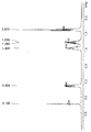
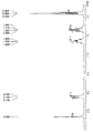
- Example 1 is a hydrogen atom nuclear magnetic resonance ( 1 H NMR) spectrum of Na (DBG) prepared in Example 1 according to the present invention
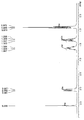
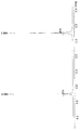
- Example 2 is a hydrogen atom nuclear magnetic resonance ( 1 H NMR) spectrum of In (DBG) 3 prepared in Example 1 according to the present invention
- TGA thermogravimetric analysis
- DTA differential thermal analysis
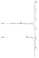
- Example 4 is a hydrogen atom nuclear magnetic resonance ( 1 H NMR) spectrum of Na (DMG) prepared in Example 2 according to the present invention
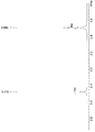
- Example 5 is a hydrogen atom nuclear magnetic resonance ( 1 H NMR) spectrum of In (DMG) 3 prepared in Example 2 according to the present invention.
- Example 6 is a hydrogen atom nuclear magnetic resonance ( 1 H NMR) spectrum of In (DEG) 3 prepared in Example 3 according to the present invention.
- Example 7 is a hydrogen atom nuclear magnetic resonance ( 1 H NMR) spectrum of In (DPG) 3 prepared in Example 4 according to the present invention.
- Example 8 is a hydrogen atom nuclear magnetic resonance ( 1 H NMR) spectrum of In (EMG) 3 prepared in Example 5 according to the present invention.
- TGA thermogravimetric analysis
- DTA differential thermal analysis
- Example 11 is a hydrogen atom nuclear magnetic resonance ( 1 H NMR) spectrum of Ga (DMG) 3 prepared in Example 7 according to the present invention.
- Example 12 is a hydrogen atom nuclear magnetic resonance ( 1 H NMR) spectrum of Ga (DEG) 3 prepared in Example 8 according to the present invention.
- Example 13 is a hydrogen atom nuclear magnetic resonance ( 1 H NMR) spectrum of Ga (DPG) 3 prepared in Example 9 according to the present invention.
- Example 14 is a hydrogen atom nuclear magnetic resonance ( 1 H NMR) spectrum of Ga (EMG) 3 prepared in Example 10 according to the present invention.
- the dibutylglycine ester (15 g, 0.07 mol) and sodium hydroxide (2.8 g, 0.07 mol) prepared in the above step were refluxed in excess distilled water (20 mL) for 3 hours, and ethanol produced as a by-product. After the water was removed, a powdery phase was obtained. The obtained powder was dissolved in methanol again, and excess acetone was added to precipitate sodium dibutylglycine, which was filtered and dried to obtain purified sodium dibutylglycine (Na (DBG)).
- 1 is a hydrogen atom nuclear magnetic resonance ( 1 H NMR) spectrum of the Na (DBG).
- Indium bromide (InBr 3 , 1 g, 2.8 mmol, 1eq) and sodium dibutylglycine (1.7 g, 8.4 mmol, 3eq) were added to 100 mL of toluene, stirred at room temperature for 12 hours, and the sodium bromide formed as a by-product was filtered. Remove and remove the solvent of the solution to afford the title compound.
- FIG. 2 is a hydrogen atom nuclear magnetic resonance ( 1 H NMR) spectrum of the indium (III) dibutylglycine (In (DBG) 3 ), and FIG. 3 is thermogravimetric analysis (TGA) and differential thermal analysis (DTA) (10). °C / min to 800 °C, 100 cc / min N2 purge) is a graph showing the results. Residual material at about 364 ° C. was about 3.5%.
- Dimethylglycine ester (15 g, 0.07 mol) and sodium hydroxide (2.8 g, 0.07 mol) were refluxed in an excess of distilled water (20 mL) for 3 hours. Obtained. The obtained powder was dissolved in methanol again, and excess acetone was added to precipitate sodium dimethylglycine, which was filtered and dried to obtain purified sodium dimethylglycine (Na (DMG)).
- DMG purified sodium dimethylglycine
- Figure 4 shows the hydrogen atom nuclear magnetic resonance ( 1 H NMR) spectrum of Na (DMG).
- Indium bromide (InBr 3 , 1 g, 2.8 mmol, 1eq) and sodium dimethylglycine (1.1 g, 8.4 mmol, 3eq) were added to 100 mL of toluene, stirred at room temperature for 12 hours, and the sodium bromide formed as a by-product was filtered off. The solvent in the solution was removed to afford the title compound (In (DMG) 3 ).
- Indium bromide (InBr 3 , 1 g, 2.8 mmol, 1eq) and sodium diethylglycine (1.3 g, 8.4 mmol, 3eq) were added to 100 mL of toluene, stirred at room temperature for 12 hours, and the sodium chloride formed as a by-product was filtered off. And the solvent in the solution was removed to afford the title compound.
- Indium bromide (InBr 3 , 1 g, 2.8 mmol, 1eq) and sodium dipropylglycine (1.5 g, 8.4 mmol, 3eq) were added to 100 mL of toluene, stirred at room temperature for 12 hours, and the sodium chloride formed as a by-product was filtered off. And the solvent in the solution was removed to afford the title compound.
- Indium bromide (InBr 3 , 1 g, 2.8 mmol, 1eq) and sodium ethylmethylglycine (1.2 g, 8.4 mmol, 3eq) were added to 100 mL of toluene, stirred at room temperature for 12 hours, and the sodium chloride formed as a by-product was filtered off. And the solvent in the solution was removed to afford the title compound.
- Gallium chloride (GaCl 3 , 1 g, 8.7 mmol, 1eq) and sodium dibutylglycine (5.5 g, 26.1 mmol, 3eq) were added to 100 mL of toluene, stirred at room temperature for 12 hours, and the resulting sodium chloride was filtered off. And the solvent in the solution is removed to afford the title compound.
- FIG. 9 is a hydrogen atom nuclear magnetic resonance ( 1 H NMR) spectrum of the gallium (III) dibutyl glycine (Ga (DBG) 3 ),
- Figure 10 is thermogravimetric analysis (TGA) and differential thermal analysis (DTA) (10 °C / min to 800 °C, 100 cc / min N 2 purge) is a graph showing the results. Weight reduction began at 84 ° C. with about 22% residual material at 284 ° C.
- Gallium chloride (GaCl 3 , 1 g, 8.7 mmol, 1eq) and sodium dimethylglycine (3.3 g, 26.1 mmol, 3eq) were added to 100 mL of toluene, stirred at room temperature for 12 hours, and the resulting sodium chloride was filtered off. The solvent in the solution was removed to afford the title compound.
- FIG. 11 shows hydrogen atom nuclear magnetic resonance ( 1 H NMR) spectra of Ga (DMG) 3.
- FIG. 11 shows hydrogen atom nuclear magnetic resonance ( 1 H NMR) spectra of Ga (DMG) 3.
- Gallium chloride (GaCl 3 , 1 g, 8.7 mmol, 1eq) and sodium diethylglycine (4.0 g, 26.1 mmol, 3eq) were added to 100 mL of toluene, stirred at room temperature for 12 hours, and the resulting sodium chloride was filtered off. And the solvent in the solution was removed to afford the title compound.
- Gallium chloride (GaCl 3 , 1 g, 8.7 mmol, 1eq) and sodium dipropylglycine (4.7 g, 26.1 mmol, 3eq) were added to 100 mL of toluene, stirred at room temperature for 12 hours, and the resulting sodium chloride was filtered off. And the solvent in the solution was removed to afford the title compound.
- FIG. 13 shows hydrogen atom nuclear magnetic resonance ( 1 H NMR) spectra of Ga (DPG) 3.
- Gallium chloride (GaCl 3 , 1 g, 8.7 mmol, 1eq) and sodium ethylmethylglycine (3.6 g, 26.1 mmol, 3eq) were added to 100 mL of toluene, stirred at room temperature for 12 hours, and the resulting sodium chloride was filtered off. And the solvent in the solution was removed to afford the title compound.
- the metal dialkylglycine compounds according to the present invention have high industrial applicability because they are stable in moisture, easy to store and have thermal stability.
- indium oxide nanoparticles, gallium oxide nanoparticles, composite metal materials including indium, and composite metal materials including gallium are prepared using the novel indium dialkylglycine compound and gallium dialkylglycine compound according to the present invention.
- indium dialkylglycine compound and gallium dialkylglycine compound according to the present invention there is an advantage in that three metal thin films including indium oxide thin film, gallium oxide thin film and indium or gallium may be manufactured through metal organic chemical vapor deposition (MOCVD).
- MOCVD metal organic chemical vapor deposition
Landscapes
- Chemical & Material Sciences (AREA)
- Organic Chemistry (AREA)
Abstract
본 발명은 변형된 글리신을 사용한 신규의 금속 디알킬글리신 및 이의 제조방법에 관한 것으로, 수분에서 안정하고 보관이 용이하며 열적 안정성이 있는 금속 디알킬글리신 및 이의 제조 방법에 관한 것이다.
Description
본 발명은 신규한 인듐 또는 갈륨 3가의 디알킬글리신 화합물에 관한 것으로서, 보다 상세하게는 인듐 또는 갈륨을 포함하는 물질을 제조하는데 전구체로서 유용한 금속 디알킬글리신 화합물 및 그 제조 방법에 관한 것이다.
인듐은 전기 도금을 통한 인듐 코팅분야에 있어 마모에 대한 저항력이 뛰어난 점과 알루미늄 전선에 접촉 시 저항이 낮다는 특성 때문에 유용하게 활용되고 있으며 유럽 지역에 있어 나트륨 가스램프(sodium vapor lamp)의 내부 코팅 재료로 산화 인듐이 이용되기도 한다. 또한 산화 인듐과 산화 주석-인듐 필름은 유리나 세라믹의 전도성을 띤 코팅 재료와 전자 발광 패널(electroluminescent pannels)에도 이용된다. 또한 산화 인듐은 열 절연체(heat insulator)로서 이용될 수 있고 태양 전지나 반도체 산업에도 응용될 수 있다 (M. Veith, S. Hill, V. Huch, Eur. J. Inorg. Chem., 1999, 1343). 또한 광전극 물질(photoelectrode material), 액정 표시 장치(liquid crystal display), 광기전 장치(photovoltaic device) 등에도 이용 가능하다 (C. R. Patra, A. Gedanken, New. J.Chem., 2004, 28, 1060).
산화 인듐 증착에 사용되어온 전구체로서 InCl3는 박막 증착 시에 염소 오염이 있을 수 있고 외부로부터 산소 원을 필요로 하는 단점이 있으며, Me3In나 Et3In 등의 트리알킬인듐(III)은 휘발성이 좋으나 산소와 수분에 매우 민감하다는 단점이 있다(C. Xu, T. H. Baum, I. Guzei, A. L. Rheingold, Inorg. Chem., 2000, 39, 2008).
또한 [In(OC2H4OMe)3]m, [In(OC2H4NMe2)3]m 등의 인듐 알콕사이드는 휘발성도 없고 공기 중에서 불안정하여 사용에 어려움이 많은 것으로 알려져 있다 (S. Daniele, D. Tchebou, L. G. Hubert-Pfalzgraf, S. Lecocq, Inorg. Chem. Comm., 2002, 5, 347). 또 다른 전구체로 In(thd)3 (여기서 thd는 2,2,6,6-테트라메틸-3,5-헵타디오네이트이다)와 In(acac)3 (여기서 acac는 acetylacetonate이다)와 같은 베타디케토네이트 리간드를 이용한 화합물이 있다 (P. Lobinger, H. S. Park, H. Hohmeister, H. W. Roesky, Chem. Vap. Deposition, 2001, 7, 105). 그러나 이들 베타디케토네이트 리간드를 이용한 화합물을 이용하여 인듐을 포함하는 재료를 만드는 경우 산소와 탄소의 오염으로 인하여 막의 성질이 나빠지는 단점이 있다.
또 다른 전구체로 [Et2InOH·Et2InNH2], [iPr2InOH·iPr2InNH2]와 같은 물과 InR3 (여기서 R은 Et2, iPr2) 유도체의 알케인 제거 반응을 이용한 화합물이 있다. (Peter Lobinger, Hyung S. Park, Holger Hohmeister, and Herbert W. Roesky, Chem. Vap. Deposition., 2001, 7, 105). 그러나 이 인듐 화합물은 암모니아를 첨가해 줌으로써 인듐 옥사이드 박막을 고온에서 증착할 수 있다. 또한 단순한 알콕사이드 리간드 대신에 두 자리 리간드를 사용하여 금속의 배위 자리를 포화시키는 방법이 알려져 있으며 또한 두 자리 리간드 중에서도 아미노 알콕사이드 계통이 알콕시 알콕사이드보다 더 유용하다고 알려져 있다 (L. G. Hubert-Pfalzgraf, H. Guillon, Appl. Organomet. Chem.,1998, 12, 221).
일반적으로 진공 공정으로 박막을 제조하기 위해서 해당 전구체가 높은 휘발성을 가져야 하고, 용액 공정을 이용하여 나노 물질을 제조하기 위해서는 전구체가 공기 중에서 안정하고 다루기 쉬워야 한다. 최근에는 인듐 화합물이 다른 금속과 함께 사용되어 인듐-갈륨-아연 산화물 (indium-gallium-zinc oxide, IGZO)와 같은 투명전자소자나 구리-인듐-갈륨 셀레나이드 (copper indium gallium selenide, CIGS)와 같은 무기태양전지소재를 제작하기 위한 전구체로 많이 연구하고 있다.
미국 특허 제 6,127,202호는 나노입자 합성 단계에서 Cu-In-O, Cu-(In,Ga) -O(이하 CI, CIG 산화물) 산화물 전구체를 합성한 뒤 이를 이용하여 다시 CIS 및 CIGS 광흡수층을 제조하는 방법을 보고하였다. 반면, 전착법은 이러한 전구체 합성 공정 같은 추가 공정 없이 CIGS 박막을 제조할 수 있어 공정을 단순화 할 수 있다. 전착법을 이용한 CIGS박막 공정에 대해서도 몇 가지 기술이 제안 되었다. 국제 특허(PCT) 제 WO01/078154호는 용액 상에서 전착법으로 CIGS 박막을 제조하는 방법에 대하여 보고하였다. 이 방법은 박막의 갈륨 조성비를 높이기 위하여 용액에 Sodium Dodecyl Sulfate(SDS, C12H25SO4Na) 등과 같은 계면활성제를 추가로 첨가하기 때문에 유기물에 의한 박막의 오염을 피할 수 없다는 것이 단점으로 지적되었다. 한편, 국제 특허 제 WO01/078154호는 전착법으로 형성된 CIGS박막을 이용하여 태양전지를 제조하여 9% 대의 에너지 효율을 보고하였다. 하지만, 이 방법에서는 추가적으로 물리증착법(PVD, Physical Vapor Deposition)을 사용하여 CIGS 박막의 부족한 인듐 성분을 보충하였다.
갈륨 옥사이드(Ga2O3)는 가스 센서(gas sensors), 투과성 전도체( transparent conductor), 형광체(phosphor) 등에 대한 새로운 물질로서 관심을 받고 있으며 넓은 밴드 갭 화합물(wide band gap compound, 4.8 eV)로써 다른 화합물의 첨가에 의해 산소가 약간 부족한 상태에서는 n-타입 반도체(n-type semiconductor)가 된다. 또한 Ga2O3는 상온에서는 전기 절연체(electrical insulator)이고, 화학적, 열적으로 안정한 단사결정계 형태(monoclinic form)를 갖는 500 ℃ 이상의 온도에서는 반도체(semiconducting)이다. 900 ℃ 이상에서는 산소의 농도에 의존해 전기 전도성이 변하기 때문에 산소의 농도(oxygen concentration)를 검출할 수 있다. 900 ℃ 이하에서는 에탄올과 같은 가스를 줄이기 위한 표면 조절 형태의 센서(surface-control-type sensor)로 작용한다. 그러므로 온도에 따른 가스 센서(gas sensor)로 이용할 수 있다. (J. S. Kim, S. B. Lee, J. H. Bahng, J. C. Choi, H. L. Park, S. I. Mho, T. W. Kim, Y. H. Whang, G. C. Kim, Phys. Stat. Sol. , 2001, 187, 569; S. Basharat, C. J. Carmalt, S. J. King, E. S. Peters, D. A. Tocher, Dalton Trans., 2004, 3475; R. Binions, C. J. Carmalt, I. P. Parkin, K. F. E. Pratt, G. A. Shaw, Chem. Mater., 2004, 16, 2489 ). 그리고 β-Ga2O3와 비결정성(amorphous) Ga2O3는 박막 전기 발광 소자(thin-film electroluminescent (TFEL) devices)에서의 새로운 형광 임자(phosphor host) 물질로서 집중을 받고 있다. 또한 Ga2O3:Mn, Ga2O3:Cr, Ga2O3:Eu는 박막 방출 층(thin-film emitting layer)과 두꺼운 세라믹 절연층(thick ceramic insulating layer)에서 높은 발광 다색 방출(high luminescence multicolor emissions)이 관찰되었다. (T. Miyata, T. Nakatani, T. Minami, Thin Solid Films, 2000, 373, 145; T. Minami, H. Yamada, Y. Kubota, T. Miyata, Jpn. J. Appl. Phys., 1997, 31, L1191; T. Xiao, A. H. Kitai, G. Liu, A. Nakua, J. Barbier, Appl. Phys. Lett., 1998, 72, 3356) 또한 전사법(lithography), 표면 개질(surface modification), 음이온 발생 (anion generation), 멸균 등의 목적으로 자외선 이용이 증가되고 있는데, 넓은 영역의 자외선 광학(deep UV optics)과 융화할 수 있는 물질의 중요성 또한 증대되고 있다. 이러한 관점에서 주석(tin)이 도핑된 β-Ga2O3 막은 넓은 영역의자외선 빛을 투과함과 동시에 전기전도성을 나타내는 독특한 산화물 막(oxide film)이라고 할 수 있다.(M. Orita, H. Hiramatsu, H. Ohta, M. Hirano, H. Hosono, Thin Solid Films, 2002, 411, 134; M. Orita, H. Hirano, H. Hosono, Appl. Phys. Lett., 2000, 77, 4166).
산화 갈륨 증착에 사용되고 있는 전구체로는 [Ga(hfac)]3 (hfac = hexafluoroacetoacetonate), [Ga(OCH(CF3)2)3(HNMe2)]등과 같은 불소(fluorine)를 포함하는 화합물과 [Ga(OBut)3]2, [Ga(OPri)3]4, [Ga(OCMe2Et)3]2 등의 갈륨 알콕사이드가 알려져 있다. 그러나 위에서 언급된 화합물들은 박막 증착 시 불소에 의해 불화갈륨(GaF3)이 형성되어 박막에 오염을 일으키며 알콕사이드 형태의 화합물은 단위체가 아니기 때문에 휘발성이 좋지 않은 단점을 가지고 있다. (G. A. Battiston, R. Gerbasi, M. Porchia, R. Bertoncello, F. Caccavale, Thin Solid Films, 1996, 279,115; L. Miinea, S. Suh, S. G. Bott, J.-R. Liu, W.-K. Chu, D. M. Hoffmam, J. Mater. Chem., 1999, 9, 929; M. Valet, D. M. Hoffman, Chem. mater., 2001, 13, 2135).
일반적으로 박막이나 나노 물질용 전구체를 고안하고 합성하기 위하여 높은 휘발성을 갖는 화합물의 합성이 가장 중요한 문제가 되고 있는데 단순한 알콕사이드 리간드 대신에 두 자리 리간드를 사용하여 금속의 배위 자리를 포화시키는 방법이 알려져 있으며 또한 두 자리 리간드 중에서도 아미노 알콕사이드 계통이 알콕시알콕사이드보다 더 유용하다고 알려져 있다 (L. G. Hubert-Pfalzgraf, H. Guillon, Appl. Organomet. Chem., 1998, 12, 221).
Ga(ORf)3(HNME2), Rf= CH(CF3)2, CMe2(CF3), CMe(CF3)2 이와 같은 불소화 알콕사이드 (fluorinated alkoxide) 유도체는 휘발성과 안전성이 강화될 뿐만 아니라 낮은 함량의 불소를 포함하는 옥사이드 박막 (oxide thin films)을 형성 한다 (Miinea, L.; Suh, S.; Bott, S.G.; J.-R.; Chu, W.-K.; Hoffman, D.M. J.Mater. Chem., 1999, 9, 929).
불소 알코올 리간드 (fluoro alcohol ligands)에 치환된 아미도 또는 이미노의 도입은 간단한 불소 알코올 리간드 (fluoro alcohol ligands)와 비교하여 첨가된 N→Ga 결합 때문에 독특한 구조적인 성질과 강화된 반응성을 나타낸다 (Yun Chi, T. Y. Chou, Y. J. Wang, S. F. Huang, A. J. Carty, L. Scoles, K. A. Udachin, S. M. Peng, G. H. Lee. Organometallics. 2004, 23, 95).
대한민국 특허 공개번호 10-2008-0066866 에 의하면, 산화 갈륨(Ga2O3)-산화아연 (ZnO) 계 스퍼터링 타겟 (GZO 계 타겟)은 특정 원소(산화지르코늄 (ZrO2), 산화알루미늄 (Al2O3))를 미량 첨가하여 도전성과 타겟의 벌크 밀도를 개선하는, 즉 성분 조성을 개선하여 소결 밀도를 올려 노듈의 형성을 억제하고, 이상 방전 및 파티클의 발생을 방지할 수 있는 타겟을 얻음과 함께 동일 타겟을 이용하여 투명 도전막을 형성한다.
산화 갈륨이 넓은 밴드갭과 높은 유전상수를 갖기 때문에 질화갈륨 나노선을 이용한 트랜지스터 산화 갈륨은 게이트 절연막의 역할을 수행할 수 있다. 대한민국 특허 공개번호 10-2008-0010062 에 의하면, 질화갈륨/산화 갈륨 나노케이블을 이용하면 소자 구현 및 집적화에 유리하게 하나의 1차원 나노구조체가 반도체/절연체 역할을 수행한다.
대한민국 특허 공개번호 10-2006-0007366 에 의하면, 크래킹이나 쌍정화 경향을 감소시키고, 결정성을 향상시킨 β-Ga2O3계 단결정, 고품질의 박막 단결정을 형성할 수 있는 박막 단결정을 성장 하고, 적외 영역에서 발광하는 Ga2O3계 발광 소자는 β-Ga2O3 단결정에 n형 불순물을 첨가하여 얻게 된 n형 기판과, 이 n형 기판의 상면에 β-Ga2O3 단결정에 p형 불순물을 첨가하여 얻게 된 p형층을 접합하여 그 접합부 부근에서 발광한다.
일반적으로 진공 공정으로 박막을 제조하기 위해서 해당 전구체가 높은 휘발성을 가져야 하고, 용액 공정을 이용하여 나노 물질을 제조하기 위해서는 전구체가 공기 중에서 안정하고 다루기 쉬워야 한다.
저온 폴리 실리콘(Low Temperature Poly-Silicon; LTPS)을 이용한 종래의 박막 트랜지스터 제조 방법은 레이저 열처리 등과 같은 고가의 공정이 포함되고 특성 제어가 어렵기 때문에 대면적의 기판에 적용이 어려운 문제점이 있다. 이러한 문제점을 해결하기 위해 최근에는 산화물 반도체를 활성층으로 이용하는 연구가 진행되고 있는데 최근 들어 비정질 상태의 InGaZnO(Indium-Gallium-Zinc oxide; 이하, IGZO라 한다)를 활성층으로 이용하는 박막트랜지스터가 제안되었다. IGZO로 이루어진 활성층은 10㎠/Vs 정도의 높은 이동도를 가지기 때문에 소자 특성을 향상시킬 수 있다.(K. Nomura et al., Nature (London) 432, 488 (2004) 및 H. Yabuta et al., Appl. Phys. Lett. 89, 112123 (2006))
IGZO와 같은 산화물 반도체에서 인듐(In)의 양을 증가시키면 케리어(전자)의 이동도가 증가되고, 갈륨(Ga)의 양을 증가시키면 케리어(전자)의 농도가 감소된다.대한민국 공개특허 10-2009-0007921에서는 IGZO와 같은 산화물 반도체에 함유된 인듐(In)의 양을 종래보다 증가시킬 수 있는 반도체 활성층 제조 방법을 제공하였다. InGaZnO로 이루어진 제 1 타겟으로부터 In, Ga 및 Zn을 포함하는 이온이 증착되어 기판 상에 IGZO층이 형성되도록 하며, InZnO로 이루어진 제 2 타겟으로부터 In을 포함하는 이온이 증착되어 In의 조성비가 증가되도록 하였다. 또 무기태양전지소재를 제작하기 위한 전구체로 구리-인듐-갈륨 셀레나이드 (copper indium gallium selenide, CIGS)를 많이 연구하고 있다.
이상과 같이 종래에 알려진 인듐 또는 갈륨 3가 화합물은 박막을 진공 공정에서 요구하는 충분하지 못한 휘발성, 제조된 막에 생기는 불소(fluorine) 오염 등의 문제점, 용액 공정에서 필요로 하는 공기 중에서 안정하고 적절한 온도에서 분해가 일어나지 않는 문제점을 가지고 있다. 따라서 용액 공정을 이용하여 산화 인듐, 산화갈륨, 인듐을 포함하는 복합 물질 또는 갈륨을 포함하는 복합 물질을 제조하기 위해서 전구체로서 화합물 자체에 할로겐을 사용하지 않고 공기 중에서 안정하며 나노 물질의 용이한 합성을 위해 유기 용매에 용해도가 좋으며 낮은 온도에서도 분해될 수 있는 인듐 또는 갈륨 3가 화합물의 개발은 그 의미가 상당히 크다고 할 수 있다.
본 발명은 새로운 리간드를 도입하여 인듐 금속 또는 갈륨 금속에 여러 전자 주개 리간드가 배위하도록 함으로써 탄소나 할로겐의 오염을 일으키지 않으며 수분에서 안정하여 다루기 쉽고 보관이 용이하며 열적 안정성이 개선된 신규의 인듐 디알킬글리신 화합물 및 그 제조 방법을 제공하는 것이다.
본 발명은 상기 목적을 달성하기 위하여, 하기 화학식 1로 표시되는 금속 디알킬글리신 화합물을 제공한다.
[화학식 1]

[상기 화학식 1에서, A는 In 또는 Ga이고, R1 및 R2는 서로 독립적으로 선형 또는 분지형의 C1-C5의 알킬기이다.]
상기의 화학식 1의 화합물은 William P. Schaefer (Journal of the American Chemical Society 91(6), 1319, 1969)의 실험방법을 참고하여 제조한 디알킬글리신 에스터를 다시 수산화나트륨과 반응하여 나트륨 디알킬글리신을 제조한 후 상기 나트륨 디알킬글리신과 인듐염 화합물 또는 갈륨염 화합물을 반응시켜 수득할 수 있다.
구체적으로 상기 화학식 1에서 R1 및 R2는 서로 독립적으로 CH3, C2H5, C3H7 또는 C4H9로부터 선택되는 것이 바람직하다.
이하, 본 발명에 따른 금속 디알킬글리신 화합물의 제조방법을 상세히 설명한다.
본 발명에 따른 상기 화학식 1의 금속 디알킬글리신 화합물은, 출발 물질로서 하기 화학식 2로 표시되는 금속 할라이드 화합물과, 하기 화학식 3으로 표시되는 나트륨 디알킬글리신을 유기용매 하에서 반응시켜 제조할 수 있으며, 이에 대한 반응은 하기 반응식 1로 나타낼 수 있다.
[화학식 2]
AX3
[화학식 3]
NaOCOCH2NR1R2
[상기 화학식 2 내지 화학식 3에서, A는 In 또는 Ga이고, X는 Cl, Br 또는 I이고, R1 및 R2는 서로 독립적으로 C1-C5의 선형 또는 분지형의 알킬기이다.]
구체적으로 상기 R1 및 R2는 서로 독립적으로 CH3, C2H5, C3H7 또는 C4H9로부터 선택되는 것이 바람직하다.
상기 반응식 1을 보다 구체적으로 설명하면, 출발 물질인 상기 화학식 2로 표시되는 금속 할라이드 화합물 1 당량과, 화학식 3의 나트륨 디알킬글리신 3 당량을 톨루엔과 같은 유기용매에서 6 내지 12 시간 동안 반응시키고 여과한 다음, 여과액으로부터 감압 하에서 용매를 제거하여 화학식 1의 화합물을 얻을 수 있다.
상기 화학식 2의 금속 할라이드화합물로 바람직하게는 브롬화인듐, 염화갈륨 등을 사용할 수 있고, 상기 화학식 3의 나트륨 디알킬글리신은 나트륨 디메틸글리신, 나트륨 디에틸글리신, 나트륨 디프로필글리신, 나트륨 디부틸글리신에서 선택되는 1종 또는 2종 이상의 혼합물이 바람직하게 사용될 수 있으나, 이에 한정되는 것은 아니다.
본 발명에 따른 금속 디알킬글리신 화합물의 제조방법에서 반응 용매는 특별히 한정되지는 않고 탄화수소 용매이면 가능하며, 특히 톨루엔, 메탄올, 에탄올, 벤젠, n-햅탄, 테트라하이드로퓨란(THF), 또는 이들의 혼합용매가 바람직하다.
또한 상기 반응 시 반응온도는 상온 내지 110℃에서 수행되나, 특별히 가온하지 않고 상온에서 6 내지 12 시간이면 반응이 완결된다.
본 발명에서 합성한 인듐 디알킬글리신 화합물 및 갈륨 디알킬글리신 화합물의 특성을 분석하기 위하여 수소 핵자기 공명 스펙트럼 (1H NMR)과 각 화합물의 열적 안정성, 휘발성, 분해 온도는 열무게 분석/시차 열분석법(thermogravimetric/differential thermal analysis, TG/DTA)을 이용하여 조사하였다.
도 1, 도 2, 도 4, 도 5, 도 6, 도 7 및 도 8은 각각 실시 예1과 실시 예1 내지 5에서 합성한 나트륨 디부틸글리신, 인듐 디부틸글리신(이하 In(DBG)3)과 나트륨 디메틸글리신, 인듐 디메틸글리신(이하 In(DMG)3), 인듐 디에틸글리신(이하 In(DEG)3), 인듐 디프로필글리신(이하 In(DPG)3), 인듐 에틸메틸글리신(이하 In(EMG)3)의 수소 원자 핵자기 공명 스펙트럼이다.
도 3에 In(DBG)3의 TG 그래프 (10 ℃/min to 800 ℃, 100 cc/min N2 purge)를 도시하였다. 364 ℃에서 잔류 물질이 약 3.5% 정도 되었다.
도 9, 도 11, 도 12, 도 13, 도14는 각각 실시 예6 내지 10에서 합성한 갈륨 디부틸글리신(이하 Ga(DBG)3)과 갈륨 디메틸글리신(이하 Ga(DMG)3), 갈륨 디에틸글리신(이하 Ga(DEG)3), 갈륨 디프로필글리신(이하 Ga(DPG)3), 갈륨 에틸메틸글리신(이하 Ga(EMG)3)의 수소 원자 핵자기 공명 스펙트럼이다.
도 10에 Ga(DBG)3의 TG/DTA 그래프 (10 ℃/min to 800 ℃, 100 cc/min N2 purge)를 도시하였다. 84 ℃에서 무게 감소가 시작되어 284 ℃에서 잔류 물질이 약 22% 정도 되었다.
실시 예에서 얻은 인듐(III) 디알킬글리신 화합물 및 갈륨(III) 디알킬글리신 화합물은 새로운 리간드를 도입하여 인듐 금속에 여러 전자 주개 리간드가 배위하도록 함으로써 탄소나 할로겐의 오염을 일으키지 않으며 수분에서 안정하여 다루기 쉽고 보관이 용이하며 열적 안정성이 개선된 신규의 화합물이다.
본 발명에 따른 신규의 인듐 디알킬글리신 화합물 및 갈륨 디알킬글리신 화합물을 이용하여 인듐 산화물 나노 입자, 갈륨 산화물 나노 입자, 인듐을 포함하는 복합금속 물질 및 갈륨을 포함하는 복합금속 물질을 제조할 수 있을 뿐만 아니라 금속 유기 화학 증착법(metal organic chemical vapor deposition, MOCVD)을 통하여 인듐 산화물 박막, 갈륨 산화물 박막 및 인듐 또는 갈륨을 포함하는 삼종금속 박막을 제조할 수 있는 장점이 있다.
본 발명에 따른 인듐 디알킬글리신 화합물 및 갈륨 디알킬글리신 화합물은 수분에 안정해 다루기가 쉽고, 보관이 용이하며, 열적 안정성을 나타냄으로써 인듐 산화물 나노 입자, 갈륨 산화물 나노 입자, 그리고 인듐 또는 갈륨을 포함하는 화합물을 생성할 수 있는 전구체로 유용하게 사용할 수 있는 효과가 있다.
도 1은 본 발명에 따른 실시예 1에서 제조한 Na(DBG)의 수소 원자 핵자기 공명 (1H NMR) 스펙트럼이고,
도 2는 본 발명에 따른 실시예 1에서 제조한 In(DBG)3의 수소 원자 핵자기 공명 (1H NMR) 스펙트럼이고,
도 3는 실시예 1에서 제조한 In(DBG)3 화합물의 열중량 분석(TGA) 및 시차 열분석 (DTA) 결과를 나타내는 그래프이다.
도 4는 본 발명에 따른 실시예 2에서 제조한 Na(DMG)의 수소 원자 핵자기 공명 (1H NMR) 스펙트럼이고,
도 5는 본 발명에 따른 실시예 2에서 제조한 In(DMG)3의 수소 원자 핵자기 공명 (1H NMR) 스펙트럼이다.
도 6은 본 발명에 따른 실시 예3에서 제조한 In(DEG)3의 수소 원자 핵자기 공명 (1H NMR) 스펙트럼이다.
도 7은 본 발명에 따른 실시 예4에서 제조한 In(DPG)3의 수소 원자 핵자기 공명 (1H NMR) 스펙트럼이다.
도 8은 본 발명에 따른 실시 예5에서 제조한 In(EMG)3의 수소 원자 핵자기 공명 (1H NMR) 스펙트럼이다.
도 9는 본 발명에 따른 실시 예6에서 제조한 Ga(DBG)3의 수소 원자 핵자기 공명 (1H NMR) 스펙트럼이고,
도 10은 실시 예6에서 제조한 Ga(DBG)3 화합물의 열중량 분석(TGA) 및 시차 열분석 (DTA) 결과를 나타내는 그래프이다.
도 11은 본 발명에 따른 실시 예7에서 제조한 Ga(DMG)3의 수소 원자 핵자기 공명 (1H NMR) 스펙트럼이다.
도 12는 본 발명에 따른 실시 예8에서 제조한 Ga(DEG)3의 수소 원자 핵자기 공명 (1H NMR) 스펙트럼이다.
도 13은 본 발명에 따른 실시 예9에서 제조한 Ga(DPG)3의 수소 원자 핵자기 공명 (1H NMR) 스펙트럼이다.
도 14는 본 발명에 따른 실시 예10에서 제조한 Ga(EMG)3의 수소 원자 핵자기 공명 (1H NMR) 스펙트럼이다.
본 발명은 하기의 실시 예에 의하여 더 잘 이해할 수 있으며, 하기의 실시 예는 본 발명의 예시 목적을 위한 것이며 첨부한 특허 청구 범위에 의하여 한정되는 보호 범위를 제한하고자 하는 것은 아니다.
[실시 예]
모든 실험은 장갑 상자 또는 슐렝크 관 (Schlenk line)을 이용하여 비활성 아르곤 또는 질소 분위기에서 수행하였다. 실시예 1 내지 5에서 각각 얻은 반응 생성물의 구조와 물성은 수소 원자 핵자기 공명법 (1H nuclear magnetic resonance, NMR), 열무게 분석/시차 열분석법 (Thermogravimetric/differential thermal analysis, TG/DTA)을 이용하여 확인하였다.
[실시 예1] 인듐(III) 디부틸글리신의 제조
디부틸글리신 에스터의 제조
에틸 클로로아세테이트(10 g, 0.082 mol)와 2당량의 디부틸아민(21 g, 0.164 mol)을 앱솔루트 에탄올 100 mL에서 환류반응으로 15 시간 반응시켰다. 반응이 끝난 후 상온으로 냉각하였다. 이때 결정성의 부산물이 석출되는데 분리를 위하여 디에틸에테르를 과량 첨가하고 이것을 필터하였다. 걸러진 용액은 다시 증류하여 디부틸글리신 에스터를 얻었다.(100℃, 10-1 torr)
나트륨 디부틸글리신의 제조
상기 단계에서 제조된 디부틸글리신 에스터(15 g, 0.07 mol)와 수산화나트륨(2.8 g, 0.07 mol)을 과량의 증류수(20 mL)에서 3 시간동안 환류반응을 한 후, 부산물로 생성된 에탄올과 물을 제거한 후 분말 상을 수득하였다. 수득된 분말을 다시 메탄올에 녹인 후 과량의 아세톤을 넣어 나트륨 디부틸글리신을 석출시키고 이것을 여과 및 건조시켜 정제된 나트륨 디부틸글리신(Na(DBG))을 수득하였다.
도 1은 상기 Na(DBG)의 수소 원자 핵자기 공명 (1H NMR) 스펙트럼이다.
인듐(III) 디부틸글리신(In(DBG)
3
)의 제조
브롬화인듐(InBr3, 1 g, 2.8 mmol, 1eq)과 나트륨 디부틸글리신(1.7 g, 8.4 mmol, 3eq)을 톨루엔 100 mL에 넣고 상온에서 12시간 교반시킨 후, 부산물로 생긴 브롬화나트륨은 여과하여 제거하고, 용액의 용매를 제거하여 표제 화합물을 수득하였다.
도 2는 상기 인듐(III) 디부틸글리신(In(DBG)3)의 수소 원자 핵자기 공명 (1H NMR) 스펙트럼이고, 도 3은 열중량 분석(TGA) 및 시차 열분석(DTA)(10 ℃/min to 800 ℃, 100 cc/min N2 purge) 결과를 나타내는 그래프이다. 364 ℃에서 잔류 물질이 약 3.5% 정도였다.
[실시 예2] 인듐(III) 디메틸글리신의 제조
나트륨 디메틸글리신의 제조
디메틸글리신 에스터(15 g, 0.07 mol)와 수산화나트륨(2.8 g, 0.07 mol)을 과량의 증류수(20 mL)에서 3 시간동안 환류반응을 한 후, 부산물로 생성된 에탄올과 물을 제거한 후 분말 상을 수득하였다. 수득된 분말을 다시 메탄올에 녹인 후 과량의 아세톤을 넣어 나트륨 디메틸글리신을 석출시키고 이것을 여과하여 건조시켜 정제된 나트륨 디메틸글리신(Na(DMG))을 수득하였다.
도 4는 Na(DMG)의 수소 원자 핵자기 공명 (1H NMR) 스펙트럼을 나타낸 것이다.
인듐(III) 디메틸글리신의 제조
브롬화인듐(InBr3, 1 g, 2.8 mmol, 1eq)와 나트륨 디메틸글리신(1.1 g, 8.4 mmol, 3eq)을 톨루엔 100 mL에 넣고 상온에서 12시간 교반시킨 후, 부산물로 생긴 브롬화나트륨은 여과하여 제거하고, 용액의 용매를 제거하여 표제 화합물(In(DMG)3)을 수득하였다.
도 5는 In(DMG)3의 수소 원자 핵자기 공명 (1H NMR) 스펙트럼을 나타낸 것이다.
[실시 예3] 인듐(III) 디에틸글리신의 제조
브롬화인듐(InBr3, 1 g, 2.8 mmol, 1eq)과 나트륨 디에틸글리신(1.3 g, 8.4 mmol, 3eq)을 톨루엔 100 mL에 넣고 상온에서 12시간 교반시킨 후, 부산물로 생긴 염화나트륨은 여과하여 제거하고, 용액의 용매를 제거하여 표제 화합물을 수득하였다.
도 6은 In(DEG)3의 수소 원자 핵자기 공명 (1H NMR) 스펙트럼을 나타낸 것이다.
[실시 예4] 인듐(III) 디프로필글리신의 제조
브롬화인듐(InBr3, 1 g, 2.8 mmol, 1eq)와 나트륨 디프로필글리신(1.5 g, 8.4 mmol, 3eq)을 톨루엔 100 mL에 넣고 상온에서 12시간 교반시킨 후, 부산물로 생긴 염화나트륨은 여과하여 제거하고, 용액의 용매를 제거하여 표제 화합물을 수득하였다.
도 7은 In(DPG)3의 수소 원자 핵자기 공명 (1H NMR) 스펙트럼을 나타낸 것이다.
[실시 예5] 인듐(III) 에틸메틸글리신의 제조
브롬화인듐(InBr3, 1 g, 2.8 mmol, 1eq)와 나트륨 에틸메틸글리신(1.2 g, 8.4 mmol, 3eq)을 톨루엔 100 mL에 넣고 상온에서 12시간 교반시킨 후, 부산물로 생긴 염화나트륨은 여과하여 제거하고, 용액의 용매를 제거하여 표제 화합물을 수득하였다.
도 8은 In(EMG)3의 수소 원자 핵자기 공명 (1H NMR) 스펙트럼을 나타낸 것이다.
[실시 예6] 갈륨(III) 디부틸글리신의 제조
갈륨(III) 디부틸글리신의 제조
염화갈륨(GaCl3, 1 g, 8.7 mmol, 1eq)와 나트륨 디부틸글리신(5.5 g, 26.1 mmol, 3eq)을 톨루엔 100 mL에 넣고 상온에서 12시간 교반시킨 후, 부산물로 생긴 염화나트륨은 여과하여 제거하고, 용액의 용매를 제거하여 표제 화합물을 수득한다.
도 9는 상기 갈륨(III) 디부틸글리신(Ga(DBG)3)의 수소 원자 핵자기 공명 (1H NMR) 스펙트럼이고, 도 10은 열중량 분석(TGA) 및 시차 열분석(DTA)(10 ℃/min to 800 ℃, 100 cc/min N2 purge) 결과를 나타내는 그래프이다. 84 ℃에서 무게 감소가 시작되어 284 ℃에서 잔류 물질이 약 22% 정도 되었다.
[실시 예7] 갈륨(III) 디메틸글리신네이트의 제조
갈륨(III) 디메틸글리신의 제조
염화갈륨(GaCl3, 1 g, 8.7 mmol, 1eq)와 나트륨 디메틸글리신(3.3 g, 26.1 mmol, 3eq)을 톨루엔 100 mL에 넣고 상온에서 12시간 교반시킨 후, 부산물로 생긴 염화나트륨은 여과하여 제거하고, 용액의 용매를 제거하여 표제 화합물을 수득하였다.
도 11은 Ga(DMG)3의 수소 원자 핵자기 공명 (1H NMR) 스펙트럼을 나타낸 것이다.
[실시 예8] 갈륨(III) 디에틸글리신의 제조
염화갈륨(GaCl3, 1 g, 8.7 mmol, 1eq)와 나트륨 디에틸글리신(4.0 g, 26.1 mmol, 3eq)을 톨루엔 100 mL에 넣고 상온에서 12시간 교반시킨 후, 부산물로 생긴 염화나트륨은 여과하여 제거하고, 용액의 용매를 제거하여 표제 화합물을 수득하였다.
도 12는 Ga(DEG)3의 수소 원자 핵자기 공명 (1H NMR) 스펙트럼을 나타낸 것이다.
[실시 예9] 갈륨(III) 디프로필글리신의 제조
염화갈륨(GaCl3, 1 g, 8.7 mmol, 1eq)와 나트륨 디프로필글리신(4.7 g, 26.1 mmol, 3eq)을 톨루엔 100 mL에 넣고 상온에서 12시간 교반시킨 후, 부산물로 생긴 염화나트륨은 여과하여 제거하고, 용액의 용매를 제거하여 표제 화합물을 수득하였다.
도 13은 Ga(DPG)3의 수소 원자 핵자기 공명 (1H NMR) 스펙트럼을 나타낸 것이다.
[실시 예10] 갈륨(III) 에틸메틸글리신의 제조
염화갈륨(GaCl3, 1 g, 8.7 mmol, 1eq)와 나트륨 에틸메틸글리신(3.6 g, 26.1 mmol, 3eq)을 톨루엔 100 mL에 넣고 상온에서 12시간 교반시킨 후, 부산물로 생긴 염화나트륨은 여과하여 제거하고, 용액의 용매를 제거하여 표제 화합물을 수득하였다.
도 14는 Ga(EMG)3의 수소 원자 핵자기 공명 (1H NMR) 스펙트럼을 나타낸 것이다.
본 발명에 따른 금속 디알킬글리신 화합물은 수분에서 안정하고 보관이 용이하며 열적 안정성이 있어 산업상 이용 가능성이 높다.
구체적으로, 본 발명에 따른 신규의 인듐 디알킬글리신 화합물 및 갈륨 디알킬글리신 화합물을 이용하여 인듐 산화물 나노 입자, 갈륨 산화물 나노 입자, 인듐을 포함하는 복합금속 물질 및 갈륨을 포함하는 복합금속 물질을 제조할 수 있을 뿐만 아니라 금속 유기 화학 증착법(metal organic chemical vapor deposition, MOCVD)을 통하여 인듐 산화물 박막, 갈륨 산화물 박막 및 인듐 또는 갈륨을 포함하는 삼종금속 박막을 제조할 수 있는 장점이 있다.
Claims (6)
- 하기 화학식 1로 표시되는 금속 디알킬글리신 화합물.[화학식 1]
 [상기 화학식 1에서, A는 In 또는 Ga이고, R1 및 R2는 서로 독립적으로 선형 또는 분지형의 C1-C5의 알킬기이다.]
 - 제 1 항에 있어서,상기 R1 및 R2는 독립적으로 CH3, C2H5, C3H7 또는 C4H9로부터 선택되는 금속 디알킬글리신 화합물.
- 하기 화학식 2로 표시되는 금속 할라이드 화합물과 하기 화학식 3으로 표시되는 나트륨 디알킬글리을 반응시키는 것을 특징으로 하는 화학식 1의 금속 디알킬글리신 화합물의 제조방법.[화학식 1]
 [화학식 2]AX3[화학식 3]NaOCOCH2NR1R2[상기 화학식 1 내지 화학식 3에서, A는 In 또는 Ga이고, X는 Cl, Br 또는 I이고, R1 및 R2는 서로 독립적으로 C1-C5의 선형 또는 분지형의 알킬기이다.]
 - 제 1항 또는 제 2항에 따른 금속 디알킬글리신 화합물을 전구체로 사용하는 금속 산화물 박막.
- 제 4항에 있어서,상기 박막은 금속 유기 화학 증착법(MOCVD)으로 형성되는 금속 산화물 박막.
- 제 1항 또는 제 2항에 따른 금속 디알킬글리신 화합물을 전구체로 사용하는 금속 나노 입자.
Applications Claiming Priority (4)
| Application Number | Priority Date | Filing Date | Title |
|---|---|---|---|
| KR10-2010-0014231 | 2010-02-17 | ||
| KR1020100014231A KR101187353B1 (ko) | 2010-02-17 | 2010-02-17 | 신규의 인듐 디알킬글리신 화합물 및 그 제조 방법 |
| KR1020100014241A KR101187700B1 (ko) | 2010-02-17 | 2010-02-17 | 신규의 갈륨 디알킬글리신 화합물 및 그 제조 방법 |
| KR10-2010-0014241 | 2010-02-17 |
Publications (1)
| Publication Number | Publication Date |
|---|---|
| WO2011102584A1 true WO2011102584A1 (ko) | 2011-08-25 |
Family
ID=44483152
Family Applications (1)
| Application Number | Title | Priority Date | Filing Date |
|---|---|---|---|
| PCT/KR2010/006959 Ceased WO2011102584A1 (ko) | 2010-02-17 | 2010-10-12 | 신규의 금속 디알킬글리신 화합물 및 그 제조 방법 |
Country Status (1)
| Country | Link |
|---|---|
| WO (1) | WO2011102584A1 (ko) |
Cited By (1)
| Publication number | Priority date | Publication date | Assignee | Title |
|---|---|---|---|---|
| WO2014027747A1 (ko) * | 2012-08-14 | 2014-02-20 | 지에스칼텍스(주) | Cis계 또는 cigs계 태양전지용 광흡수층의 제조방법 및 cis계 또는 cigs계 태양전지용 광흡수 잉크 |
-
2010
- 2010-10-12 WO PCT/KR2010/006959 patent/WO2011102584A1/ko not_active Ceased
Non-Patent Citations (4)
| Title |
|---|
| CARMALT, C. J. ET AL.: "Gallium (III) and Indium (III) Alkoxides and Aryloxides.", COORD. CHEM. REV., vol. 250, March 2006 (2006-03-01), pages 682 - 709, XP005294599 * |
| CARPENTIER, J. -F.: "Multidentate Fluorinated Alkoxide Ligand Platforms for Oxophilic Metal Centers: from MOCVD Source Reagents to Polymerization Catalysts.", DALTON TRANS., vol. 39, 17 September 2009 (2009-09-17), pages 37 - 48 * |
| CHOU T. -Y.: "Fluorinated Aminoalkoxide and Ketoiminate Indium Complexes as MOCVD Precursors for In203 Thin Film Deposition.", INORG. CHEM., vol. 42, 28 August 2003 (2003-08-28), pages 6041 - 6049 * |
| KOCHETKOV, A. P. ET AL.: "Compounds of Indium with Glycocoll.", ZHUMAL NEORGANICHESKOI KHIMII, vol. 8, no. 3, 1963, USSR, pages 772 - 774 * |
Cited By (1)
| Publication number | Priority date | Publication date | Assignee | Title |
|---|---|---|---|---|
| WO2014027747A1 (ko) * | 2012-08-14 | 2014-02-20 | 지에스칼텍스(주) | Cis계 또는 cigs계 태양전지용 광흡수층의 제조방법 및 cis계 또는 cigs계 태양전지용 광흡수 잉크 |
Similar Documents
| Publication | Publication Date | Title |
|---|---|---|
| TWI519510B (zh) | 用以製備氯二烷醇銦之方法 | |
| KR101404714B1 (ko) | 단차피복성이 우수한 루테늄 화합물 및 이를 이용하여 증착시킨 박막 | |
| KR102935328B1 (ko) | 인듐 전구체 화합물, 이를 이용한 박막의 제조 방법 및 이로부터 제조된 기판 | |
| KR101629696B1 (ko) | 신규한 인듐 전구체, 이의 제조 방법 및 이를 이용한 박막 | |
| Ahmed et al. | Semiconducting composite oxide Y 2 CuO 4–5CuO thin films for investigation of photoelectrochemical properties | |
| US8097302B2 (en) | Electroconductive tin oxide having high mobility and low electron concentration | |
| KR100897495B1 (ko) | 신규의 갈륨 아미노알콕사이드 화합물 및 그 제조방법 | |
| US9812330B2 (en) | Formulations for producing indium oxide-containing layers, process for producing them and their use | |
| WO2011102584A1 (ko) | 신규의 금속 디알킬글리신 화합물 및 그 제조 방법 | |
| KR101187700B1 (ko) | 신규의 갈륨 디알킬글리신 화합물 및 그 제조 방법 | |
| WO2015056944A1 (ko) | 몰리브데넘 화합물 또는 텅스텐 화합물, 이의 제조 방법 및 이를 이용하여 박막을 형성하는 방법 | |
| KR20100054313A (ko) | 신규의 갈륨 알콕사이드 화합물 및 그 제조방법 | |
| KR101187353B1 (ko) | 신규의 인듐 디알킬글리신 화합물 및 그 제조 방법 | |
| US9802964B2 (en) | Process for preparing indium alkoxide compounds, the indium alkoxide compounds preparable by the process and the use thereof | |
| KR20200083340A (ko) | 박막 형성용 전구체, 이의 제조방법, 이를 이용한 박막의 제조 방법 및 박막 | |
| KR100982972B1 (ko) | ZnO 박막 제조용 전구체 및 이를 이용한화학기상증착법에 의한 ZnO 박막의 제조 방법 | |
| KR101255850B1 (ko) | 신규의 갈륨 글리콜레이트 화합물 및 그 제조 방법 | |
| WO2014148830A1 (ko) | 산화아연 전구체의 제조방법, 이로부터 수득되는 산화아연 전구체 및 산화아연 박막 | |
| KR100965270B1 (ko) | 새로운 전자 주개 리간드를 가지는 갈륨 착화합물 및 이의제조방법 | |
| Jain | Synthesis and purification of some main group organometallic precursors for compound semiconductors | |
| KR101242772B1 (ko) | 신규한 비스무트 아미노 알콕사이드 화합물 및 그 제조 방법 | |
| KR101190161B1 (ko) | 신규의 아연 아미노알콕사이드 화합물 및 그 제조방법 | |
| KR101124216B1 (ko) | 신규의 알칼리 토금속 디알킬글리신 화합물 및 그 제조 방법 | |
| WO2025058377A1 (ko) | 갈륨 화합물을 포함하는 박막 증착용 조성물 및 이를 이용한 박막의 제조 방법 | |
| WO2013129746A1 (ko) | 황화주석 전구체, 상기 전구체를 이용한 박막 및 그 제조 방법 |
Legal Events
| Date | Code | Title | Description |
|---|---|---|---|
| 121 | Ep: the epo has been informed by wipo that ep was designated in this application |
Ref document number: 10846222 Country of ref document: EP Kind code of ref document: A1 |
|
| NENP | Non-entry into the national phase |
Ref country code: DE |
|
| 122 | Ep: pct application non-entry in european phase |
Ref document number: 10846222 Country of ref document: EP Kind code of ref document: A1 |