WO2011093207A1 - 異方性導電フィルム、接合体及び接続方法 - Google Patents
異方性導電フィルム、接合体及び接続方法 Download PDFInfo
- Publication number
- WO2011093207A1 WO2011093207A1 PCT/JP2011/051008 JP2011051008W WO2011093207A1 WO 2011093207 A1 WO2011093207 A1 WO 2011093207A1 JP 2011051008 W JP2011051008 W JP 2011051008W WO 2011093207 A1 WO2011093207 A1 WO 2011093207A1
- Authority
- WO
- WIPO (PCT)
- Prior art keywords
- conductive film
- mass
- circuit member
- anisotropic conductive
- resin
- Prior art date
- Legal status (The legal status is an assumption and is not a legal conclusion. Google has not performed a legal analysis and makes no representation as to the accuracy of the status listed.)
- Ceased
Links
Images


Classifications
-
- C—CHEMISTRY; METALLURGY
- C08—ORGANIC MACROMOLECULAR COMPOUNDS; THEIR PREPARATION OR CHEMICAL WORKING-UP; COMPOSITIONS BASED THEREON
- C08L—COMPOSITIONS OF MACROMOLECULAR COMPOUNDS
- C08L71/00—Compositions of polyethers obtained by reactions forming an ether link in the main chain; Compositions of derivatives of such polymers
-
- H—ELECTRICITY
- H01—ELECTRIC ELEMENTS
- H01B—CABLES; CONDUCTORS; INSULATORS; SELECTION OF MATERIALS FOR THEIR CONDUCTIVE, INSULATING OR DIELECTRIC PROPERTIES
- H01B5/00—Non-insulated conductors or conductive bodies characterised by their form
- H01B5/16—Non-insulated conductors or conductive bodies characterised by their form comprising conductive material in insulating or poorly conductive material, e.g. conductive rubber
-
- C—CHEMISTRY; METALLURGY
- C08—ORGANIC MACROMOLECULAR COMPOUNDS; THEIR PREPARATION OR CHEMICAL WORKING-UP; COMPOSITIONS BASED THEREON
- C08K—Use of inorganic or non-macromolecular organic substances as compounding ingredients
- C08K3/00—Use of inorganic substances as compounding ingredients
- C08K3/02—Elements
- C08K3/08—Metals
-
- C—CHEMISTRY; METALLURGY
- C08—ORGANIC MACROMOLECULAR COMPOUNDS; THEIR PREPARATION OR CHEMICAL WORKING-UP; COMPOSITIONS BASED THEREON
- C08L—COMPOSITIONS OF MACROMOLECULAR COMPOUNDS
- C08L33/00—Compositions of homopolymers or copolymers of compounds having one or more unsaturated aliphatic radicals, each having only one carbon-to-carbon double bond, and only one being terminated by only one carboxyl radical, or of salts, anhydrides, esters, amides, imides or nitriles thereof; Compositions of derivatives of such polymers
- C08L33/04—Homopolymers or copolymers of esters
- C08L33/06—Homopolymers or copolymers of esters of esters containing only carbon, hydrogen and oxygen, which oxygen atoms are present only as part of the carboxyl radical
-
- C—CHEMISTRY; METALLURGY
- C09—DYES; PAINTS; POLISHES; NATURAL RESINS; ADHESIVES; COMPOSITIONS NOT OTHERWISE PROVIDED FOR; APPLICATIONS OF MATERIALS NOT OTHERWISE PROVIDED FOR
- C09J—ADHESIVES; NON-MECHANICAL ASPECTS OF ADHESIVE PROCESSES IN GENERAL; ADHESIVE PROCESSES NOT PROVIDED FOR ELSEWHERE; USE OF MATERIALS AS ADHESIVES
- C09J11/00—Features of adhesives not provided for in group C09J9/00, e.g. additives
- C09J11/02—Non-macromolecular additives
-
- C—CHEMISTRY; METALLURGY
- C09—DYES; PAINTS; POLISHES; NATURAL RESINS; ADHESIVES; COMPOSITIONS NOT OTHERWISE PROVIDED FOR; APPLICATIONS OF MATERIALS NOT OTHERWISE PROVIDED FOR
- C09J—ADHESIVES; NON-MECHANICAL ASPECTS OF ADHESIVE PROCESSES IN GENERAL; ADHESIVE PROCESSES NOT PROVIDED FOR ELSEWHERE; USE OF MATERIALS AS ADHESIVES
- C09J5/00—Adhesive processes in general; Adhesive processes not provided for elsewhere, e.g. relating to primers
- C09J5/06—Adhesive processes in general; Adhesive processes not provided for elsewhere, e.g. relating to primers involving heating of the applied adhesive
-
- C—CHEMISTRY; METALLURGY
- C09—DYES; PAINTS; POLISHES; NATURAL RESINS; ADHESIVES; COMPOSITIONS NOT OTHERWISE PROVIDED FOR; APPLICATIONS OF MATERIALS NOT OTHERWISE PROVIDED FOR
- C09J—ADHESIVES; NON-MECHANICAL ASPECTS OF ADHESIVE PROCESSES IN GENERAL; ADHESIVE PROCESSES NOT PROVIDED FOR ELSEWHERE; USE OF MATERIALS AS ADHESIVES
- C09J7/00—Adhesives in the form of films or foils
- C09J7/10—Adhesives in the form of films or foils without carriers
-
- C—CHEMISTRY; METALLURGY
- C09—DYES; PAINTS; POLISHES; NATURAL RESINS; ADHESIVES; COMPOSITIONS NOT OTHERWISE PROVIDED FOR; APPLICATIONS OF MATERIALS NOT OTHERWISE PROVIDED FOR
- C09J—ADHESIVES; NON-MECHANICAL ASPECTS OF ADHESIVE PROCESSES IN GENERAL; ADHESIVE PROCESSES NOT PROVIDED FOR ELSEWHERE; USE OF MATERIALS AS ADHESIVES
- C09J9/00—Adhesives characterised by their physical nature or the effects produced, e.g. glue sticks
- C09J9/02—Electrically-conducting adhesives
-
- G—PHYSICS
- G02—OPTICS
- G02F—OPTICAL DEVICES OR ARRANGEMENTS FOR THE CONTROL OF LIGHT BY MODIFICATION OF THE OPTICAL PROPERTIES OF THE MEDIA OF THE ELEMENTS INVOLVED THEREIN; NON-LINEAR OPTICS; FREQUENCY-CHANGING OF LIGHT; OPTICAL LOGIC ELEMENTS; OPTICAL ANALOGUE/DIGITAL CONVERTERS
- G02F1/00—Devices or arrangements for the control of the intensity, colour, phase, polarisation or direction of light arriving from an independent light source, e.g. switching, gating or modulating; Non-linear optics
- G02F1/01—Devices or arrangements for the control of the intensity, colour, phase, polarisation or direction of light arriving from an independent light source, e.g. switching, gating or modulating; Non-linear optics for the control of the intensity, phase, polarisation or colour
- G02F1/13—Devices or arrangements for the control of the intensity, colour, phase, polarisation or direction of light arriving from an independent light source, e.g. switching, gating or modulating; Non-linear optics for the control of the intensity, phase, polarisation or colour based on liquid crystals, e.g. single liquid crystal display cells
- G02F1/133—Constructional arrangements; Operation of liquid crystal cells; Circuit arrangements
- G02F1/1333—Constructional arrangements; Manufacturing methods
- G02F1/1345—Conductors connecting electrodes to cell terminals
-
- H—ELECTRICITY
- H10—SEMICONDUCTOR DEVICES; ELECTRIC SOLID-STATE DEVICES NOT OTHERWISE PROVIDED FOR
- H10W—GENERIC PACKAGES, INTERCONNECTIONS, CONNECTORS OR OTHER CONSTRUCTIONAL DETAILS OF DEVICES COVERED BY CLASS H10
- H10W72/00—Interconnections or connectors in packages
- H10W72/071—Connecting or disconnecting
- H10W72/073—Connecting or disconnecting of die-attach connectors
-
- H—ELECTRICITY
- H10—SEMICONDUCTOR DEVICES; ELECTRIC SOLID-STATE DEVICES NOT OTHERWISE PROVIDED FOR
- H10W—GENERIC PACKAGES, INTERCONNECTIONS, CONNECTORS OR OTHER CONSTRUCTIONAL DETAILS OF DEVICES COVERED BY CLASS H10
- H10W72/00—Interconnections or connectors in packages
- H10W72/30—Die-attach connectors
-
- C—CHEMISTRY; METALLURGY
- C08—ORGANIC MACROMOLECULAR COMPOUNDS; THEIR PREPARATION OR CHEMICAL WORKING-UP; COMPOSITIONS BASED THEREON
- C08G—MACROMOLECULAR COMPOUNDS OBTAINED OTHERWISE THAN BY REACTIONS ONLY INVOLVING UNSATURATED CARBON-TO-CARBON BONDS
- C08G2650/00—Macromolecular compounds obtained by reactions forming an ether link in the main chain of the macromolecule
- C08G2650/28—Macromolecular compounds obtained by reactions forming an ether link in the main chain of the macromolecule characterised by the polymer type
- C08G2650/56—Polyhydroxyethers, e.g. phenoxy resins
-
- C—CHEMISTRY; METALLURGY
- C08—ORGANIC MACROMOLECULAR COMPOUNDS; THEIR PREPARATION OR CHEMICAL WORKING-UP; COMPOSITIONS BASED THEREON
- C08K—Use of inorganic or non-macromolecular organic substances as compounding ingredients
- C08K3/00—Use of inorganic substances as compounding ingredients
- C08K3/02—Elements
- C08K3/08—Metals
- C08K2003/0862—Nickel
-
- C—CHEMISTRY; METALLURGY
- C08—ORGANIC MACROMOLECULAR COMPOUNDS; THEIR PREPARATION OR CHEMICAL WORKING-UP; COMPOSITIONS BASED THEREON
- C08K—Use of inorganic or non-macromolecular organic substances as compounding ingredients
- C08K2201/00—Specific properties of additives
- C08K2201/001—Conductive additives
-
- C—CHEMISTRY; METALLURGY
- C08—ORGANIC MACROMOLECULAR COMPOUNDS; THEIR PREPARATION OR CHEMICAL WORKING-UP; COMPOSITIONS BASED THEREON
- C08K—Use of inorganic or non-macromolecular organic substances as compounding ingredients
- C08K9/00—Use of pretreated ingredients
- C08K9/02—Ingredients treated with inorganic substances
-
- C—CHEMISTRY; METALLURGY
- C09—DYES; PAINTS; POLISHES; NATURAL RESINS; ADHESIVES; COMPOSITIONS NOT OTHERWISE PROVIDED FOR; APPLICATIONS OF MATERIALS NOT OTHERWISE PROVIDED FOR
- C09J—ADHESIVES; NON-MECHANICAL ASPECTS OF ADHESIVE PROCESSES IN GENERAL; ADHESIVE PROCESSES NOT PROVIDED FOR ELSEWHERE; USE OF MATERIALS AS ADHESIVES
- C09J11/00—Features of adhesives not provided for in group C09J9/00, e.g. additives
- C09J11/02—Non-macromolecular additives
- C09J11/06—Non-macromolecular additives organic
-
- C—CHEMISTRY; METALLURGY
- C09—DYES; PAINTS; POLISHES; NATURAL RESINS; ADHESIVES; COMPOSITIONS NOT OTHERWISE PROVIDED FOR; APPLICATIONS OF MATERIALS NOT OTHERWISE PROVIDED FOR
- C09J—ADHESIVES; NON-MECHANICAL ASPECTS OF ADHESIVE PROCESSES IN GENERAL; ADHESIVE PROCESSES NOT PROVIDED FOR ELSEWHERE; USE OF MATERIALS AS ADHESIVES
- C09J2203/00—Applications of adhesives in processes or use of adhesives in the form of films or foils
- C09J2203/326—Applications of adhesives in processes or use of adhesives in the form of films or foils for bonding electronic components such as wafers, chips or semiconductors
-
- C—CHEMISTRY; METALLURGY
- C09—DYES; PAINTS; POLISHES; NATURAL RESINS; ADHESIVES; COMPOSITIONS NOT OTHERWISE PROVIDED FOR; APPLICATIONS OF MATERIALS NOT OTHERWISE PROVIDED FOR
- C09J—ADHESIVES; NON-MECHANICAL ASPECTS OF ADHESIVE PROCESSES IN GENERAL; ADHESIVE PROCESSES NOT PROVIDED FOR ELSEWHERE; USE OF MATERIALS AS ADHESIVES
- C09J2301/00—Additional features of adhesives in the form of films or foils
- C09J2301/20—Additional features of adhesives in the form of films or foils characterized by the structural features of the adhesive itself
- C09J2301/208—Additional features of adhesives in the form of films or foils characterized by the structural features of the adhesive itself the adhesive layer being constituted by at least two or more adjacent or superposed adhesive layers, e.g. multilayer adhesive
-
- C—CHEMISTRY; METALLURGY
- C09—DYES; PAINTS; POLISHES; NATURAL RESINS; ADHESIVES; COMPOSITIONS NOT OTHERWISE PROVIDED FOR; APPLICATIONS OF MATERIALS NOT OTHERWISE PROVIDED FOR
- C09J—ADHESIVES; NON-MECHANICAL ASPECTS OF ADHESIVE PROCESSES IN GENERAL; ADHESIVE PROCESSES NOT PROVIDED FOR ELSEWHERE; USE OF MATERIALS AS ADHESIVES
- C09J2301/00—Additional features of adhesives in the form of films or foils
- C09J2301/40—Additional features of adhesives in the form of films or foils characterized by the presence of essential components
- C09J2301/408—Additional features of adhesives in the form of films or foils characterized by the presence of essential components additives as essential feature of the adhesive layer
-
- C—CHEMISTRY; METALLURGY
- C09—DYES; PAINTS; POLISHES; NATURAL RESINS; ADHESIVES; COMPOSITIONS NOT OTHERWISE PROVIDED FOR; APPLICATIONS OF MATERIALS NOT OTHERWISE PROVIDED FOR
- C09J—ADHESIVES; NON-MECHANICAL ASPECTS OF ADHESIVE PROCESSES IN GENERAL; ADHESIVE PROCESSES NOT PROVIDED FOR ELSEWHERE; USE OF MATERIALS AS ADHESIVES
- C09J2433/00—Presence of (meth)acrylic polymer
-
- C—CHEMISTRY; METALLURGY
- C09—DYES; PAINTS; POLISHES; NATURAL RESINS; ADHESIVES; COMPOSITIONS NOT OTHERWISE PROVIDED FOR; APPLICATIONS OF MATERIALS NOT OTHERWISE PROVIDED FOR
- C09J—ADHESIVES; NON-MECHANICAL ASPECTS OF ADHESIVE PROCESSES IN GENERAL; ADHESIVE PROCESSES NOT PROVIDED FOR ELSEWHERE; USE OF MATERIALS AS ADHESIVES
- C09J2461/00—Presence of condensation polymers of aldehydes or ketones
-
- C—CHEMISTRY; METALLURGY
- C09—DYES; PAINTS; POLISHES; NATURAL RESINS; ADHESIVES; COMPOSITIONS NOT OTHERWISE PROVIDED FOR; APPLICATIONS OF MATERIALS NOT OTHERWISE PROVIDED FOR
- C09J—ADHESIVES; NON-MECHANICAL ASPECTS OF ADHESIVE PROCESSES IN GENERAL; ADHESIVE PROCESSES NOT PROVIDED FOR ELSEWHERE; USE OF MATERIALS AS ADHESIVES
- C09J4/00—Adhesives based on organic non-macromolecular compounds having at least one polymerisable carbon-to-carbon unsaturated bond ; adhesives, based on monomers of macromolecular compounds of groups C09J183/00 - C09J183/16
-
- H—ELECTRICITY
- H10—SEMICONDUCTOR DEVICES; ELECTRIC SOLID-STATE DEVICES NOT OTHERWISE PROVIDED FOR
- H10W—GENERIC PACKAGES, INTERCONNECTIONS, CONNECTORS OR OTHER CONSTRUCTIONAL DETAILS OF DEVICES COVERED BY CLASS H10
- H10W72/00—Interconnections or connectors in packages
- H10W72/071—Connecting or disconnecting
- H10W72/072—Connecting or disconnecting of bump connectors
-
- H—ELECTRICITY
- H10—SEMICONDUCTOR DEVICES; ELECTRIC SOLID-STATE DEVICES NOT OTHERWISE PROVIDED FOR
- H10W—GENERIC PACKAGES, INTERCONNECTIONS, CONNECTORS OR OTHER CONSTRUCTIONAL DETAILS OF DEVICES COVERED BY CLASS H10
- H10W72/00—Interconnections or connectors in packages
- H10W72/071—Connecting or disconnecting
- H10W72/073—Connecting or disconnecting of die-attach connectors
- H10W72/07331—Connecting techniques
- H10W72/07332—Compression bonding, e.g. thermocompression bonding
-
- H—ELECTRICITY
- H10—SEMICONDUCTOR DEVICES; ELECTRIC SOLID-STATE DEVICES NOT OTHERWISE PROVIDED FOR
- H10W—GENERIC PACKAGES, INTERCONNECTIONS, CONNECTORS OR OTHER CONSTRUCTIONAL DETAILS OF DEVICES COVERED BY CLASS H10
- H10W72/00—Interconnections or connectors in packages
- H10W72/071—Connecting or disconnecting
- H10W72/073—Connecting or disconnecting of die-attach connectors
- H10W72/07331—Connecting techniques
- H10W72/07337—Connecting techniques using a polymer adhesive, e.g. an adhesive based on silicone or epoxy
- H10W72/07338—Connecting techniques using a polymer adhesive, e.g. an adhesive based on silicone or epoxy hardening the adhesive by curing, e.g. thermosetting
-
- H—ELECTRICITY
- H10—SEMICONDUCTOR DEVICES; ELECTRIC SOLID-STATE DEVICES NOT OTHERWISE PROVIDED FOR
- H10W—GENERIC PACKAGES, INTERCONNECTIONS, CONNECTORS OR OTHER CONSTRUCTIONAL DETAILS OF DEVICES COVERED BY CLASS H10
- H10W72/00—Interconnections or connectors in packages
- H10W72/071—Connecting or disconnecting
- H10W72/074—Connecting or disconnecting of anisotropic conductive adhesives
-
- H—ELECTRICITY
- H10—SEMICONDUCTOR DEVICES; ELECTRIC SOLID-STATE DEVICES NOT OTHERWISE PROVIDED FOR
- H10W—GENERIC PACKAGES, INTERCONNECTIONS, CONNECTORS OR OTHER CONSTRUCTIONAL DETAILS OF DEVICES COVERED BY CLASS H10
- H10W72/00—Interconnections or connectors in packages
- H10W72/20—Bump connectors, e.g. solder bumps or copper pillars; Dummy bumps; Thermal bumps
- H10W72/241—Dispositions, e.g. layouts
-
- H—ELECTRICITY
- H10—SEMICONDUCTOR DEVICES; ELECTRIC SOLID-STATE DEVICES NOT OTHERWISE PROVIDED FOR
- H10W—GENERIC PACKAGES, INTERCONNECTIONS, CONNECTORS OR OTHER CONSTRUCTIONAL DETAILS OF DEVICES COVERED BY CLASS H10
- H10W72/00—Interconnections or connectors in packages
- H10W72/30—Die-attach connectors
- H10W72/321—Structures or relative sizes of die-attach connectors
- H10W72/322—Multilayered die-attach connectors, e.g. a coating on a top surface of a core
-
- H—ELECTRICITY
- H10—SEMICONDUCTOR DEVICES; ELECTRIC SOLID-STATE DEVICES NOT OTHERWISE PROVIDED FOR
- H10W—GENERIC PACKAGES, INTERCONNECTIONS, CONNECTORS OR OTHER CONSTRUCTIONAL DETAILS OF DEVICES COVERED BY CLASS H10
- H10W72/00—Interconnections or connectors in packages
- H10W72/30—Die-attach connectors
- H10W72/321—Structures or relative sizes of die-attach connectors
- H10W72/325—Die-attach connectors having a filler embedded in a matrix
-
- H—ELECTRICITY
- H10—SEMICONDUCTOR DEVICES; ELECTRIC SOLID-STATE DEVICES NOT OTHERWISE PROVIDED FOR
- H10W—GENERIC PACKAGES, INTERCONNECTIONS, CONNECTORS OR OTHER CONSTRUCTIONAL DETAILS OF DEVICES COVERED BY CLASS H10
- H10W72/00—Interconnections or connectors in packages
- H10W72/30—Die-attach connectors
- H10W72/351—Materials of die-attach connectors
-
- H—ELECTRICITY
- H10—SEMICONDUCTOR DEVICES; ELECTRIC SOLID-STATE DEVICES NOT OTHERWISE PROVIDED FOR
- H10W—GENERIC PACKAGES, INTERCONNECTIONS, CONNECTORS OR OTHER CONSTRUCTIONAL DETAILS OF DEVICES COVERED BY CLASS H10
- H10W72/00—Interconnections or connectors in packages
- H10W72/30—Die-attach connectors
- H10W72/351—Materials of die-attach connectors
- H10W72/352—Materials of die-attach connectors comprising metals or metalloids, e.g. solders
-
- H—ELECTRICITY
- H10—SEMICONDUCTOR DEVICES; ELECTRIC SOLID-STATE DEVICES NOT OTHERWISE PROVIDED FOR
- H10W—GENERIC PACKAGES, INTERCONNECTIONS, CONNECTORS OR OTHER CONSTRUCTIONAL DETAILS OF DEVICES COVERED BY CLASS H10
- H10W72/00—Interconnections or connectors in packages
- H10W72/30—Die-attach connectors
- H10W72/351—Materials of die-attach connectors
- H10W72/353—Materials of die-attach connectors not comprising solid metals or solid metalloids, e.g. ceramics
- H10W72/354—Materials of die-attach connectors not comprising solid metals or solid metalloids, e.g. ceramics comprising polymers
-
- H—ELECTRICITY
- H10—SEMICONDUCTOR DEVICES; ELECTRIC SOLID-STATE DEVICES NOT OTHERWISE PROVIDED FOR
- H10W—GENERIC PACKAGES, INTERCONNECTIONS, CONNECTORS OR OTHER CONSTRUCTIONAL DETAILS OF DEVICES COVERED BY CLASS H10
- H10W90/00—Package configurations
- H10W90/701—Package configurations characterised by the relative positions of pads or connectors relative to package parts
- H10W90/731—Package configurations characterised by the relative positions of pads or connectors relative to package parts of die-attach connectors
- H10W90/734—Package configurations characterised by the relative positions of pads or connectors relative to package parts of die-attach connectors between a chip and a stacked insulating package substrate, interposer or RDL
Definitions
- the present invention relates to an anisotropic conductive film having high conduction reliability and high adhesive strength, and particularly suitable for connection between COF and PWB, a bonded body using the anisotropic conductive film, and a connection method.
- a COF Chip On Film
- FPC flexible substrate
- PWB printed wiring board
- ACF anisotropic conductive film
- the LCD and COF, or the COF and PWB are ACF-connected so that electrical connection can be obtained between the adjacent electrodes, and insulation between the adjacent electrodes is maintained, and the LCD and COF or the COF and PWB are externally connected.
- the function of adhesion is also given so that it does not peel off with the force of.
- the pattern positional deviation accuracy during ACF thermocompression bonding becomes severe.
- the LCD side pattern and the COF pattern, and the COF pattern and the PWB side pattern are difficult to be misaligned.
- the former is a fine pitch, but the LCD side is glass, so the amount of thermal expansion is stable. This can be dealt with by correcting the pitch in advance.
- the thickness of the PWB glass and epoxy material is not stable in quality, the amount of thermal expansion is not stable, and the degree of positional displacement is high.
- the FR-4 standard of general-purpose PWB has a glass transition temperature (Tg) of 110 ° C to 130 ° C, and considering the reduction of PWB warpage and ACF connection damage, the temperature during crimping may be lower. preferable. Therefore, a low temperature connection is required for the connection between COF and PWB. Furthermore, in recent years, a demand for a short-time connection has been increasing in order to improve productivity.
- Tg glass transition temperature
- the adhesive strength (90 ° Y-axis peel strength of the COF and PWB joints) ) Tend to be low. This is because the binder quickly solidifies in the low temperature region, so that the polyimide material on the COF side and the binder are not sufficiently wetted and it is difficult to form a chemical bond, and the cured binder is hard and the 90 ° Y-axis peel strength is high. Since the amount of deformation of the cured binder itself at the connection portion is small at the time of measurement, it can be considered that the absorbed energy for deformation is small.
- Patent Document 1 and Patent Document 2 propose an ACF using Ni fine particles.
- Patent Document 3 Patent Document 4, and Patent Document 5 propose conductive particles obtained by performing Ni plating on a resin core and Au plating on an outer shell thereof, and ACF using the same.
- Patent Document 6 proposes an ACF in which a resin core is Ni-plated and its outer shell is Ag-plated.
- Patent Document 7 proposes an ACF including hard conductive particles and soft conductive particles. As the hard conductive particles, nickel plated with gold is used, and as the soft conductive particles, crosslinked polystyrene resin particles plated with gold are used.
- the present invention makes it a subject to solve the said various problems in the past and to achieve the following objectives. That is, the present invention provides an anisotropic conductive film having high adhesive strength under low temperature short time conditions and excellent conduction reliability, a joined body using the anisotropic conductive film, and a connection method. With the goal.
- the conductive layer comprises at least a two-layer structure of an insulating layer and a conductive layer, and the insulating layer contains a monofunctional monomer in order to obtain a high adhesive force, and the conductive layer Containing two kinds of conductive particles, Ni particles for breaking through the oxide film on the PWB electrode to obtain low connection resistance and resin particles having a resin core coated with at least Ni for obtaining high conduction reliability It has been found that the conductive film has high adhesive strength and excellent conduction reliability in spite of low temperature and short time conditions.
- the present invention is based on the above findings by the present inventors, and means for solving the above problems are as follows. That is, ⁇ 1> It has at least a conductive layer and an insulating layer,
- the insulating layer contains a binder, a monofunctional polymerizable monomer, and a curing agent
- the conductive layer contains Ni particles, metal-coated resin particles, a binder, a polymerizable monomer, and a curing agent
- An anisotropic conductive film wherein the metal-coated resin particles are resin particles in which a resin core is coated with at least Ni.
- ⁇ 2> The anisotropic conductive film according to ⁇ 1>, wherein the insulating layer contains at least a phenoxy resin, a monofunctional (meth) acrylic monomer, and an organic peroxide.
- ⁇ 3> The anisotropic conductive film according to any one of ⁇ 1> to ⁇ 2>, wherein the conductive layer contains at least a phenoxy resin, a (meth) acrylic monomer, and an organic peroxide.
- ⁇ 4> The above ⁇ 1> to ⁇ 3, wherein the metal-coated resin particles are any of resin particles in which a resin core is coated with Ni and resin particles in which a resin core is coated with Ni and the outermost surface is coated with Au.
- ⁇ 7> The above ⁇ 1> to ⁇ 6>, wherein the total content of the Ni particles and the metal-coated resin particles in the conductive layer is 3.0 to 20 parts by mass with respect to 100 parts by mass of the resin solid content of the conductive layer. It is an anisotropic conductive film in any one.
- the first circuit member is a printed wiring board, The joined body according to ⁇ 8>, wherein the second circuit member is COF.
- ⁇ 10> In the method of connecting the first circuit member and the second circuit member, The anisotropic conductive film according to any one of ⁇ 1> to ⁇ 7> is sandwiched between the first circuit member and the second circuit member, By pressing while heating from the first circuit member and the second circuit member, the anisotropic conductive film is cured, and the first circuit member and the second circuit member are connected.
- This is a characteristic connection method.
- the first circuit member is a printed wiring board
- the connection method according to ⁇ 10>, wherein the second circuit member is a COF.
- ⁇ 12> The connection method according to ⁇ 11>, wherein the conductive layer of the anisotropic conductive film is disposed on the printed wiring board side and the insulating layer of the anisotropic conductive film is disposed on the COF side.
- the above-mentioned problems can be solved and the object can be achieved, and an anisotropic conductive film having high adhesive strength under low temperature and short time conditions and excellent conduction reliability, A joined body using an anisotropic conductive film and a connection method can be provided.
- FIG. 1 is a schematic view showing an example of the anisotropic conductive film of the present invention.
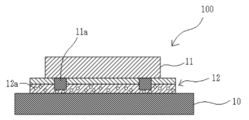
- FIG. 2 is a schematic view showing an example of the joined body of the present invention.
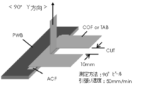
- FIG. 3 is an explanatory diagram showing a method for measuring peel strength in the examples.
- FIG. 4 is an explanatory diagram illustrating a method for measuring conduction resistance in the embodiment.
- the anisotropic conductive film of the present invention has at least a conductive layer and an insulating layer, and has a release substrate and, if necessary, other layers.
- the anisotropic conductive film may have a peeling substrate (separator), an insulating layer formed on the peeling substrate (separator), and a conductive layer formed on the insulating layer. preferable.
- the aspect which does not have a peeling base material may be sufficient as the said anisotropic conductive film, and when it has a peeling base material, a peeling base material is peeled and removed in the case of a connection.
- the insulating layer contains a binder, a monofunctional polymerizable monomer, and a curing agent, and contains a silane coupling agent and, if necessary, other components.
- a monofunctional monomer has not been used as a reaction main component of a binder of an anisotropic conductive film (ACF).
- ACF anisotropic conductive film
- the monofunctional monomer is used for the purpose of imparting tack to the film or dissolving the binder, and only the monofunctional monomer is the reactive component, and the cured binder becomes sticky or heat resistant. Since it becomes the binder hardened
- Tg glass transition temperature
- the anisotropy of the present invention having a two-layer structure having a conductive layer containing two kinds of conductive particles and an insulating layer is provided. Even if a monofunctional monomer is used for the insulating layer in the conductive film, there is no problem in the conduction characteristics.
- the anisotropic conductive film of the present invention has a configuration in which hard Ni particles contained in the conductive layer bite into the terminal, and sufficient adhesive strength (peel strength) is required to maintain the biting into the terminal.
- the binder composition includes two types of conductive particles (resin particles in which Ni particles and a resin core are coated with at least Ni) in the conductive layer, and a monofunctional monomer in the insulating layer. It will be indispensable.
- the binder is not particularly limited and may be appropriately selected depending on the intended purpose.
- phenoxy resin, epoxy resin, unsaturated polyester resin, saturated polyester resin, urethane resin, butadiene resin, polyimide resin, polyamide resin, polyolefin Resin etc. are mentioned. These may be used individually by 1 type and may use 2 or more types together.
- phenoxy resin is particularly preferable in terms of film forming property, processability, and connection reliability.
- the said phenoxy resin is resin synthesize
- the content of the binder in the insulating layer is not particularly limited and may be appropriately selected depending on the intended purpose. For example, it is preferably 20% by mass to 70% by mass, and more preferably 35% by mass to 55% by mass. preferable.
- the monofunctional polymerizable monomer is not particularly limited as long as it has one polymerizable group in the molecule, and can be appropriately selected according to the purpose.
- a monofunctional (meth) acryl monomer examples thereof include styrene monomers, butadiene monomers, and other olefinic monomers having a double bond. These may be used individually by 1 type and may use 2 or more types together.
- monofunctional (meth) acrylic monomers are particularly preferable in terms of adhesive strength and connection reliability.
- the monofunctional (meth) acrylic monomer is not particularly limited and may be appropriately selected depending on the intended purpose.
- acrylic acid methyl acrylate, ethyl acrylate, propyl acrylate, n-butyl acrylate, acrylic Acrylic acid such as isobutyl acid, n-octyl acrylate, n-dodecyl acrylate, 2-ethylhexyl acrylate, stearyl acrylate, 2-chloroethyl acrylate, phenyl acrylate, or the like; methacrylic acid, methacrylic acid Methyl acetate, ethyl methacrylate, propyl methacrylate, n-butyl methacrylate, isobutyl methacrylate, n-octyl methacrylate, n-dodecyl methacrylate, 2-ethylhexyl methacrylate, stearyl methacrylate, phenyl methacrylate, methacryl Acid dimethyl Ruaminoechiru, methacrylic
- the content of the monofunctional polymerizable monomer in the insulating layer is not particularly limited and may be appropriately selected depending on the purpose. It is preferably 2% by mass to 30% by mass, and preferably 5% by mass to 20%. More preferably, it is mass%.
- the curing agent is not particularly limited as long as it can cure the binder, and can be appropriately selected according to the purpose.
- an organic peroxide is preferable.
- the organic peroxide include lauroyl peroxide, butyl peroxide, benzyl peroxide, dilauroyl peroxide, dibutyl peroxide, benzyl peroxide, peroxydicarbonate, benzoyl peroxide, and the like. These may be used individually by 1 type and may use 2 or more types together.
- the content of the curing agent in the insulating layer is not particularly limited and may be appropriately selected depending on the purpose. It is preferably 1% by mass to 15% by mass, and preferably 3% by mass to 10% by mass. It is more preferable.
- the silane coupling agent is not particularly limited and may be appropriately selected depending on the purpose.
- an epoxy silane coupling agent, an acrylic silane coupling agent, a thiol silane coupling agent, an amine silane cup A ring agent etc. are mentioned.
- the content of the silane coupling agent in the insulating layer is not particularly limited and may be appropriately selected depending on the purpose. The content is preferably 0.5% by mass to 10% by mass, and preferably 1% by mass to 5%. More preferably, it is mass%.
- the insulating layer is prepared by, for example, preparing a coating solution for an insulating layer containing a binder, a monofunctional polymerizable monomer, a curing agent, preferably a silane coupling agent, and, if necessary, other components (such as an organic solvent). It can form by apply
- the thickness of the insulating layer is not particularly limited and may be appropriately selected depending on the purpose. For example, the thickness is preferably 10 ⁇ m to 25 ⁇ m, and more preferably 18 ⁇ m to 21 ⁇ m. If the thickness is too thin, the peel strength may be lowered. If the thickness is too thick, the conduction reliability may be deteriorated.
- the conductive layer contains Ni particles, metal-coated resin particles, a binder, a polymerizable monomer, and a curing agent, and further contains a silane coupling agent and, if necessary, other components.
- the Ni particles are used to achieve a low connection resistance.
- the Ni particles are not particularly limited and may be appropriately selected depending on the intended purpose, but the average particle size is preferably 1 ⁇ m to 5 ⁇ m. If the average particle size is less than 1 ⁇ m, there is a problem in connection reliability after crimping because the surface area is small. If the average particle size exceeds 5 ⁇ m, a short circuit between the wires may occur if the wires are fine pitch. May occur and cause problems.
- the surface of the Ni particles having metal protrusions or the surface of the Ni particles having an insulating film formed of an organic substance can also be used.
- the average particle diameter of the Ni particles represents a number average particle diameter, and can be measured by, for example, a particle size distribution measuring device (Microtrac MT3100, manufactured by Nikkiso Co., Ltd.).
- the hardness of the Ni particles is preferably, for example, 2,000kgf / mm 2 ⁇ 6,000kgf / mm 2.
- the hardness of the Ni particles can be determined from the test force when a load is applied to the Ni particles and displaced by 10%, for example, by a micro compressor test. As said Ni particle, what was synthesize
- the metal-coated resin particles are preferably resin particles in which the resin core is coated with at least Ni from the viewpoint of ensuring conduction reliability.
- the resin core is coated with Ni
- the resin core is coated with Ni
- resin particles whose outermost surface is coated with Au are listed.
- the method for coating the resin core with Ni or Au is not particularly limited and may be appropriately selected depending on the intended purpose. Examples thereof include an electroless plating method and a sputtering method.
- the material for the resin core is not particularly limited and may be appropriately selected depending on the intended purpose.
- Examples thereof include styrene-divinylbenzene copolymer, benzoguanamine resin, cross-linked polystyrene resin, acrylic resin, and styrene-silica composite resin. Can be mentioned. Among these, a styrene-divinylbenzene copolymer is particularly preferable from the viewpoint of allowing a flexible particle to have a large contact area when compressed and ensuring good conduction reliability.
- Hardness of the metal-coated resin particles is preferably, for example, 50kgf / mm 2 ⁇ 500kgf / mm 2.
- the hardness of the metal-coated resin particles can be determined from a test force when a load is applied to the metal-coated resin particles and displaced by 10%, for example, by a micro compressor test.
- the difference in hardness (AB) between the hardness (A) of the Ni particles and the hardness (B) of the metal-coated resin particles is preferably 1,500 kgf / mm 2 or more, and 2,000 kgf / mm 2 to 5 000 kgf / mm 2 is more preferable.
- the metal-coated resin particles those appropriately synthesized may be used, or commercially available products may be used.
- the average particle diameter of the metal-coated resin particles is preferably 5 ⁇ m or more, and more preferably 9 ⁇ m to 11 ⁇ m. When the average particle size is less than 5 ⁇ m, the repulsive force of the metal-coated resin particles at the time of pressure bonding is lowered, which may cause problems in connection reliability.
- the average particle diameter of the metal-coated resin particles represents a number average particle diameter, and can be measured by, for example, a particle size distribution measuring device (Microtrac MT3100, manufactured by Nikkiso Co., Ltd.).
- the content of the metal-coated resin particles in the conductive layer is not particularly limited and can be appropriately selected according to the purpose.
- the resin solid content (total amount of binder, polymerizable monomer, and curing agent) is 100 parts by mass.
- the amount is preferably 2 to 10 parts by weight, more preferably 2 to 8 parts by weight. If the content is too small, the conduction resistance may increase, and if it is too large, the risk of short circuit may increase.
- the total content of the Ni particles and the metal-coated resin particles in the conductive layer is preferably 3 parts by mass to 20 parts by mass with respect to 100 parts by mass of the resin solid content of the conductive layer. It is more preferable that If the content is too small, the conduction resistance may increase, and if it is too large, the risk of short circuit may increase.
- or polyfunctional polymerizable monomer can be used, for example, a monofunctional (meth) acryl monomer, a bifunctional (meth) acryl monomer, trifunctional ( And (meth) acrylic monomers. These may be used individually by 1 type and may use 2 or more types together.
- the content of the polymerizable monomer in the conductive layer is not particularly limited and may be appropriately selected depending on the purpose. It is preferably 3% by mass to 60% by mass, and 5% by mass to 50% by mass. More preferably.
- the binder, curing agent, silane coupling agent, and other components in the conductive layer are the same as those of the insulating layer.
- the content can be used.
- the conductive layer is prepared, for example, by applying a coating solution for a conductive layer containing Ni particles, metal-coated resin particles, a binder, a polymerizable monomer, a curing agent, preferably a silane coupling agent, and further other components as necessary. It can form by apply
- the thickness of the conductive layer is not particularly limited and may be appropriately selected depending on the purpose. For example, the thickness is preferably 10 ⁇ m to 25 ⁇ m, and more preferably 15 ⁇ m to 20 ⁇ m. If the thickness is too thin, the conduction reliability may be deteriorated, and if it is too thick, the peel strength may be lowered.
- the thickness of the anisotropic conductive film in which the insulating layer and the conductive layer are combined is preferably 25 ⁇ m to 55 ⁇ m, and more preferably 30 ⁇ m to 50 ⁇ m. If the thickness is too thin, the peel strength may be reduced due to insufficient filling, and if it is too thick, conduction failure due to insufficient push-in may occur.
- the release substrate is not particularly limited in its shape, structure, size, thickness, material (material), etc., and can be appropriately selected according to the purpose. Those having high properties are preferable, and examples thereof include a transparent release PET (polyethylene terephthalate) sheet and a PTFE (polytetrafluoroethylene) sheet coated with a release agent such as silicone.
- the thickness of the release substrate is not particularly limited and may be appropriately selected depending on the intended purpose. For example, the thickness is preferably 10 ⁇ m to 100 ⁇ m, and more preferably 20 ⁇ m to 80 ⁇ m.
- the anisotropic conductive film of the present invention includes a peeling substrate (separator) 20, an insulating layer 22 formed on the peeling substrate (separator) 20, and the insulating layer. 22 and a conductive layer 21 formed on the substrate 22.
- conductive particles 12a Ni particles and Ni / Au plated resin particles
- the conductive film 12 is attached so that the conductive layer 21 is on the PWB 10 side.
- the peeling substrate (separator) 20 is peeled off, and the COF 11 is pressure-bonded from the insulating layer 22 side, so that the joined body 100 is formed.
- the joined body of the present invention includes the first circuit member, the second circuit member, and the anisotropic conductive film of the present invention, and further includes other members as necessary.
- the first circuit member and the second circuit member are joined via the anisotropic conductive film.
- the conductive layer of the anisotropic conductive film is attached so as to be on the printed wiring board side as the first circuit member, and the release substrate is peeled off from the anisotropic conductive film.
- the insulating layer is disposed on the COF side as the second circuit member.
- connection method of the present invention is a connection method between the first circuit member and the second circuit member.
- the anisotropic conductive film of the present invention is sandwiched between the first circuit member and the second circuit member, By pressing while heating from the first circuit member and the second circuit member, the anisotropic conductive film is cured, and the first circuit member and the second circuit member are connected. is there.
- the first circuit member is a printed wiring board and the second circuit member is a COF.
- the anisotropic conductive film is disposed so that the conductive layer is on the printed wiring board side, and the insulating layer of the anisotropic conductive film is on the COF side. Is done.
- the heating is determined by the total amount of heat, and when the joining is completed within a connection time of 10 seconds or less, the heating temperature is preferably 120 ° C to 220 ° C.
- the pressure bonding differs depending on the type of the second circuit member and cannot be defined unconditionally. For example, in the case of TAB tape, the pressure is 2 MPa to 6 MPa, in the case of IC chip, the pressure is 20 MPa to 120 MPa, and in the case of COF, the pressure is 2 MPa. It is preferable to perform at 3 to 10 MPa at 3 to 10 MPa.
- the average particle diameter of the Ni particles or resin particles was measured with a particle size distribution measuring device (Microtrac MT3100, manufactured by Nikkiso Co., Ltd.).
- Electroless Ni plating is applied to the particle surface of styrene-divinylbenzene copolymer resin particles having an average particle size of 10 ⁇ m, and Au plating is further applied to the Ni plating surface by displacement plating to produce Ni / Au plated resin particles A. did.
- Example 1 ⁇ Preparation of anisotropic conductive film 1> -Production of insulating layer 1- 45 parts by mass of phenoxy resin (trade name: YP-50, manufactured by Toto Kasei Co., Ltd.), 20 parts by mass of urethane acrylate (trade name: U-2PPA, manufactured by Shin-Nakamura Chemical Co., Ltd.), monofunctional acrylic monomer (trade name: 4) -HBA, 10 parts by mass of Osaka Organic Chemical Co., Ltd., 2 parts by mass of phosphate ester acrylate (trade name: PM-2, Nippon Kayaku Co., Ltd.), benzoyl peroxide (Japan) A mixture of ethyl acetate and toluene containing 3 parts by mass of OIL Co., Ltd.
- phenoxy resin trade name: YP-50, manufactured by Toto Kasei Co., Ltd.
- U-2PPA manufactured by Shin-Nakamura Chemical Co., Ltd.
- monofunctional acrylic monomer
- conductive layer 1- 45 parts by mass of phenoxy resin (trade name: YP-50, manufactured by Toto Kasei Co., Ltd.), 20 parts by mass of urethane acrylate (trade name: U-2PPA, manufactured by Shin-Nakamura Chemical Co., Ltd.), bifunctional acrylic monomer (trade name: A -200, Shin-Nakamura Chemical Co., Ltd.) 20 parts by mass, monofunctional acrylic monomer (trade name: 4-HBA, Osaka Organic Chemical Industries, Ltd.) 10 parts by mass, phosphate ester acrylate (trade name: PM-2) 2 parts by mass, manufactured by Nippon Kayaku Co., Ltd., 3 parts by mass of benzoyl peroxide (manufactured by NOF Corporation) as an organic peroxide, and 3 parts by weight of dilauroyl peroxide (manufactured by NOF Corporation) as an organic peroxide Part by mass, Ni particles of Production Example 1 (average particle size 3 ⁇ m) 2.8 parts by mass
- this mixed solution was applied onto a polyethylene terephthalate (PET) film having a thickness of 50 ⁇ m, and then dried in an oven at 80 ° C. for 5 minutes, and the PET film was peeled off to produce a conductive layer 1 having a thickness of 17 ⁇ m.
- PET polyethylene terephthalate
- the produced insulating layer 1 and the conductive layer 1 are laminated by a roller, and bonded to form an anisotropic conductive film 1 having a two-layer structure including the insulating layer 1 and the conductive layer 1 having a total thickness of 35 ⁇ m.
- peel strength As shown in FIG. 3, 90 ° Y-axis direction peel strength was measured at a pulling speed of 50 mm / min. Since COF with respect to COF is harder to adhere than TCP, peel strength was measured based on the following criteria by measuring only COF with respect to COF. The results are shown by the maximum peel strength (N / cm). ⁇ Evaluation criteria ⁇ ⁇ : Peel strength is 8 N / cm or more ⁇ : Peel strength is less than 8 N / cm
- Example 2 ⁇ Production and Evaluation of Anisotropic Conductive Film 2>
- the conductive layer 1 was replaced with the following conductive layer 2
- the two-layer anisotropy composed of the insulating layer 1 and the conductive layer 2 having a total thickness of 35 ⁇ m was performed in the same manner as in Example 1.
- the conductive film 2 and the joined body 2 were produced.
- conductive layer 2- 45 parts by mass of phenoxy resin (trade name: YP-50, manufactured by Toto Kasei Co., Ltd.), 20 parts by mass of urethane acrylate (trade name: U-2PPA, manufactured by Shin-Nakamura Chemical Co., Ltd.), bifunctional acrylic monomer (trade name: A -200, Shin-Nakamura Chemical Co., Ltd.) 20 parts by mass, monofunctional acrylic monomer (trade name: 4-HBA, Osaka Organic Chemical Industries, Ltd.) 10 parts by mass, phosphate ester acrylate (trade name: PM-2) 2 parts by mass, manufactured by Nippon Kayaku Co., Ltd., 3 parts by mass of benzoyl peroxide (manufactured by NOF Corporation) as an organic peroxide, and 3 parts by weight of dilauroyl peroxide (manufactured by NOF Corporation) as an organic peroxide Part by mass, 2.8 parts by mass of Ni particles in Production Example 1 (average particle size 3 ⁇ m
- this mixed solution was applied onto a polyethylene terephthalate (PET) film having a thickness of 50 ⁇ m, and then dried in an oven at 80 ° C. for 5 minutes, and the PET film was peeled off to produce a conductive layer 2 having a thickness of 17 ⁇ m.
- PET polyethylene terephthalate
- Example 3 ⁇ Preparation of anisotropic conductive film 3>
- the anisotropy of the two-layer structure including the insulating layer 1 and the conductive layer 3 having a total thickness of 35 ⁇ m was performed in the same manner as in Example 1.
- the conductive film 3 and the joined body 3 were produced.
- conductive layer 3- 45 parts by mass of phenoxy resin (trade name: YP-50, manufactured by Toto Kasei Co., Ltd.), 20 parts by mass of urethane acrylate (trade name: U-2PPA, manufactured by Shin-Nakamura Chemical Co., Ltd.), bifunctional acrylic monomer (trade name: A -200, Shin-Nakamura Chemical Co., Ltd.) 20 parts by mass, monofunctional acrylic monomer (trade name: 4-HBA, Osaka Organic Chemical Industries, Ltd.) 10 parts by mass, phosphate ester acrylate (trade name: PM-2) 2 parts by mass, manufactured by Nippon Kayaku Co., Ltd., 3 parts by mass of benzoyl peroxide (manufactured by NOF Corporation) as an organic peroxide, and 3 parts by weight of dilauroyl peroxide (manufactured by NOF Corporation) as an organic peroxide Parts by mass, Ni particles of Production Example 1 (average particle size 3 ⁇ m) 2.8 parts by
- this mixed solution was applied onto a polyethylene terephthalate (PET) film having a thickness of 50 ⁇ m, and then dried in an oven at 80 ° C. for 5 minutes, and the PET film was peeled off to produce a conductive layer 3 having a thickness of 17 ⁇ m.
- PET polyethylene terephthalate
- Example 4 ⁇ Preparation of anisotropic conductive film 4>
- the conductive layer 1 was replaced with the following conductive layer 4
- the two-layer anisotropy composed of the insulating layer 1 and the conductive layer 4 having a total thickness of 35 ⁇ m was performed in the same manner as in Example 1.
- the conductive film 4 and the joined body 4 were produced.
- PET polyethylene terephthalate
- Example 5 ⁇ Preparation of anisotropic conductive film 5>
- the two-layer anisotropy composed of the insulating layer 1 and the conductive layer 5 having a total thickness of 35 ⁇ m was performed in the same manner as in Example 1.
- the conductive film 5 and the joined body 5 were produced.
- conductive layer 5- 45 parts by mass of phenoxy resin (trade name: YP-50, manufactured by Toto Kasei Co., Ltd.), 20 parts by mass of urethane acrylate (trade name: U-2PPA, manufactured by Shin-Nakamura Chemical Co., Ltd.), bifunctional acrylic monomer (trade name: A -200, Shin-Nakamura Chemical Co., Ltd.) 20 parts by mass, monofunctional acrylic monomer (trade name: 4-HBA, Osaka Organic Chemical Industries, Ltd.) 10 parts by mass, phosphate ester acrylate (trade name: PM-2) 2 parts by mass, manufactured by Nippon Kayaku Co., Ltd., 3 parts by mass of benzoyl peroxide (manufactured by NOF Corporation) as an organic peroxide, and 3 parts by weight of dilauroyl peroxide (manufactured by NOF Corporation) as an organic peroxide Parts by mass, Ni particles of Production Example 1 (average particle size 3 ⁇ m) 1.9 parts by
- this mixed solution was applied onto a polyethylene terephthalate (PET) film having a thickness of 50 ⁇ m, and then dried in an oven at 80 ° C. for 5 minutes, and the PET film was peeled off to produce a conductive layer 5 having a thickness of 17 ⁇ m.
- PET polyethylene terephthalate
- Example 1 ⁇ Preparation of anisotropic conductive film 6>
- the conductive layer 1 was replaced with the following conductive layer 6, the two-layered anisotropy composed of the insulating layer 1 having a total thickness of 35 ⁇ m and the conductive layer 6 was performed in the same manner as in Example 1.
- the conductive film 6 and the joined body 6 were produced.
- conductive layer 6- 45 parts by mass of phenoxy resin (trade name: YP-50, manufactured by Toto Kasei Co., Ltd.), 20 parts by mass of urethane acrylate (trade name: U-2PPA, manufactured by Shin-Nakamura Chemical Co., Ltd.), bifunctional acrylic monomer (trade name: A -200, Shin-Nakamura Chemical Co., Ltd.) 20 parts by mass, monofunctional acrylic monomer (trade name: 4-HBA, Osaka Organic Chemical Industries, Ltd.) 10 parts by mass, phosphate ester acrylate (trade name: PM-2) 2 parts by mass, manufactured by Nippon Kayaku Co., Ltd., 3 parts by mass of benzoyl peroxide (manufactured by NOF Corporation) as an organic peroxide, and 3 parts by weight of dilauroyl peroxide (manufactured by NOF Corporation) as an organic peroxide A mixed solution of ethyl acetate and toluene containing 2.8 parts by
- this mixed solution was applied on a polyethylene terephthalate (PET) film having a thickness of 50 ⁇ m, and then dried in an oven at 80 ° C. for 5 minutes, and the PET film was peeled off to produce a conductive layer 6 having a thickness of 17 ⁇ m.
- PET polyethylene terephthalate
- Example 2 (Comparative Example 2) ⁇ Preparation of anisotropic conductive film 7>
- the two-layer anisotropy composed of the insulating layer 1 having a total thickness of 35 ⁇ m and the conductive layer 7 was performed in the same manner as in Example 1.
- the conductive film 7 and the joined body 7 were produced.
- conductive layer 7- 45 parts by mass of phenoxy resin (trade name: YP-50, manufactured by Toto Kasei Co., Ltd.), 20 parts by mass of urethane acrylate (trade name: U-2PPA, manufactured by Shin-Nakamura Chemical Co., Ltd.), bifunctional acrylic monomer (trade name: A -200, Shin-Nakamura Chemical Co., Ltd.) 20 parts by mass, monofunctional acrylic monomer (trade name: 4-HBA, Osaka Organic Chemical Industries, Ltd.) 10 parts by mass, phosphate ester acrylate (trade name: PM-2) 2 parts by mass, manufactured by Nippon Kayaku Co., Ltd., 3 parts by mass of benzoyl peroxide (manufactured by NOF Corporation) as an organic peroxide, and 3 parts by weight of dilauroyl peroxide (manufactured by NOF Corporation) as an organic peroxide And 3.8 parts by mass of Ni / Au plated resin particles A (average particle size 10 ⁇
- PET polyethylene terephthalate
- Example 3 (Comparative Example 3) ⁇ Preparation of anisotropic conductive film 8>
- the two-layer anisotropy composed of the insulating layer 2 and the conductive layer 3 having a total thickness of 35 ⁇ m was performed in the same manner as in Example 3.
- the conductive film 8 and the joined body 8 were produced.
- insulating layer 2- 45 parts by mass of phenoxy resin (trade name: YP-50, manufactured by Toto Kasei Co., Ltd.), 20 parts by mass of urethane acrylate (trade name: U-2PPA, manufactured by Shin-Nakamura Chemical Co., Ltd.), bifunctional acrylic monomer (trade name: A -200, Shin-Nakamura Chemical Co., Ltd.) 20 parts by mass, monofunctional acrylic monomer (trade name: 4-HBA, Osaka Organic Chemical Industries, Ltd.) 10 parts by mass, phosphate ester acrylate (trade name: PM-2) 2 parts by weight, manufactured by Nippon Kayaku Co., Ltd., 3 parts by weight of benzoyl peroxide (manufactured by NOF Corporation) as an organic peroxide, and dilauroyl peroxide (manufactured by NOF Corporation) as an organic peroxide A mixed solution of ethyl acetate and toluene containing 3 parts by mass so that the solid
- this mixed solution was applied onto a polyethylene terephthalate (PET) film having a thickness of 50 ⁇ m, and then dried in an oven at 80 ° C. for 5 minutes, and the PET film was peeled off to produce an insulating layer 2 having a thickness of 18 ⁇ m.
- PET polyethylene terephthalate
- this mixed solution was applied onto a polyethylene terephthalate (PET) film having a thickness of 50 ⁇ m, dried in an oven at 80 ° C. for 5 minutes, and the PET film was peeled off, whereby the anisotropic layer comprising the conductive layer 3 having a thickness of 35 ⁇ m.
- Conductive film 9 was produced. Using this anisotropic conductive film 9, a joined body 9 was produced in the same manner as in Example 1, and peel strength and conduction resistance were measured in the same manner as in Example 1. The results are shown in Table 1.
- Examples 1 to 5 and Comparative Examples 1, 2, and 5 all show high peel strength and good adhesion despite low temperature and short time conditions of 130 ° C., 3 MPa, and 3 sec. Met. Further, Examples 1 to 5 and Comparative Examples 1, 4, and 5 were all good because the initial conduction resistance was as low as 0.06 ⁇ or less. In addition, Examples 3 and 4 and Comparative Examples 3 and 4 were all good because the conduction resistance after 1,000 hours was low under a high temperature and high humidity environment (85 ° C., 85% RH).
- Example 1 a benzoguanamine resin having an average particle size of 5 ⁇ m is used as the resin core of the metal-coated resin particles of the conductive layer, and the peel strength and initial conduction resistance are good, but the repulsive force of the resin core itself is high. It is larger than styrene-divinylbenzene copolymer, and the hardened binder is loosened by the repulsive force of the resin core in an environment of 85 ° C. and 85% RH. Therefore, it is 1 in a high temperature and high humidity environment (85 ° C., 85% RH). The conduction resistance after 3,000 hours was slightly increased.
- Example 2 cross-linked polystyrene is used as the resin core of the metal-coated resin particles of the conductive layer, and the peel strength and initial conduction resistance are good.
- the repulsive force of the resin core itself is styrene-divinyl. It is larger than benzene copolymer, and under high temperature and high humidity environment (85 ° C, 85% RH), the binder cured product holding the particles loosens under the influence of the repulsive force, resulting in 1,000 hours later.
- the conduction resistance was slightly higher.
- the insulating layer contains a monofunctional acrylic monomer
- the conductive layer contains Ni particles and Ni / Au plated resin particles A (resin core: styrene-divinylbenzene copolymer, average particle size 10 ⁇ m). It is the best mode of the invention.
- a soft styrene-divinylbenzene copolymer is used as the resin core of the metal-coated resin particles of the conductive layer, and the repulsive force is weakened. Even when only Ni plating is used, a low conductive resistance value that is not much different from Au / Ni plating is obtained after 1,000 hours in a high temperature and high humidity environment (85% RH at 85 ° C.). It was.
- Example 5 the total amount of Ni particles and Ni / Au plated resin particles A is 2.9 parts by mass with respect to 100 parts by mass of the resin solid content, and the Ni particles and Ni / Au plated resin particles of Example 3 Since the total amount of A is less than half of 6.4 parts by mass with respect to 100 parts by mass of the resin solid content, the conduction resistance after 1,000 hours under a high temperature and high humidity environment (85 ° C., 85% RH) It became high.
- Comparative Example 1 contains only Ni particles in the conductive layer, so that the peel strength and the initial conduction resistance are good, but after 1,000 hours under a high temperature and high humidity environment (85 ° C., 85% RH). The conduction resistance increased.
- Comparative Example 2 since the conductive layer does not contain Ni particles but contains Ni / Au plated resin particles A, the initial conduction resistance is slightly higher than that in Example 3 (best mode), and a high temperature and high humidity environment (85 C., 85% RH), the conduction resistance significantly increased after 1,000 hours. This is because the Ni / Au plating resin particles A alone cannot break through the oxide film formed on the surface of the PWB pattern to obtain conductivity, so that it is 1,000 in a high temperature and high humidity environment (85 ° C., 85% RH). It is thought that it rose greatly after time.
- Comparative Example 3 since the insulating layer contains a bifunctional acrylic monomer, the conduction resistance after 1,000 hours in the initial and high-temperature and high-humidity environment (85 ° C., 85% RH) is good, but the peel strength is high. Has fallen. In Comparative Example 4, the conductive layer was a single layer, and the peel strength was reduced. Comparative Example 5 is a reproduction of the example of Japanese Patent Application Laid-Open No. 11-339558. Since the conductive layer is a single layer and the curing reaction component is only a monofunctional monomer, the glass transition temperature of the binder cured product.
- Tg is low (> 85 ° C.) and loses the repulsive force of the hard particles of the resin core in a high temperature and high humidity environment (85% RH at 85 ° C.). As a result, the conduction resistance after 1,000 hours is OPEN. It became. Further, since the outer shell of the Ni particles is plated with soft Au, it is difficult to penetrate into the terminal and it is difficult to break through the oxide film. However, since the reaction component was only a monofunctional monomer and the glass transition temperature (Tg) was low, the peel strength was high.
- the anisotropic conductive film of the present invention has high adhesive strength under low temperature short time conditions and excellent conduction reliability, for example, connection between COF and PWB, connection between TCP and PWB, COF and glass substrate It is suitably used for connection between circuit members such as connection, connection between COF and COF, connection between IC substrate and glass substrate, connection between IC substrate and PWB.
Landscapes
- Chemical & Material Sciences (AREA)
- Organic Chemistry (AREA)
- Health & Medical Sciences (AREA)
- Chemical Kinetics & Catalysis (AREA)
- Medicinal Chemistry (AREA)
- Polymers & Plastics (AREA)
- Physics & Mathematics (AREA)
- Nonlinear Science (AREA)
- Crystallography & Structural Chemistry (AREA)
- Mathematical Physics (AREA)
- General Physics & Mathematics (AREA)
- Optics & Photonics (AREA)
- Adhesives Or Adhesive Processes (AREA)
- Non-Insulated Conductors (AREA)
- Adhesive Tapes (AREA)
- Chemically Coating (AREA)
Abstract
Description
この場合、LCDとCOF、又はCOFとPWBはACF接続することで、互いに電気的な接続が得られ、かつ隣接電極間で絶縁性が保たれると共に、LCDとCOF、又はCOFとPWBが外部の力で剥がれないように接着の機能も付与されている。
近年、LCDモジュールのコストダウンのために、1つのCOFを多出力化(=ファインピッチ化)することでCOFの部品点数を削減する活動が活発化されている。
一方、後者はPWBのガラスとエポキシ材料の厚みが品質的に安定していないため熱膨張量も安定せず、位置ズレ難易度が高い。また、汎用PWBのFR-4規格はガラス転移温度(Tg)が110℃~130℃であり、PWBの反りやACF接続部のダメージ低減を考慮すると、圧着時の温度はより低温であることが好ましい。そこで、COFとPWBの接続では低温接続が求められる。更に、近年では生産性向上のため、短時間接続の要求も強くなっている。
一方、90°Y軸方向ピール強度の測定時に接続部のバインダー硬化物自体の変形量を多くするために、バインダー硬化物の機械的強度(=弾性率)を低く設計すると、接着強度は上がるものの、導通信頼性が悪くなってしまう。
このように対COFの接着強度向上と、対TCP(Tape Carrier Package)の導通信頼性向上とのバランスを図ることは、極めて困難な課題の一つであった。
通常、LCDパネルにCOFを実装してLCDモジュールが完成するが、このLCDモジュールを筐体に組立てる際に、LCDパネルとCOF、COFとPWBのACF接続部に一時的な外的応力が加わる。
経験的にLCDパネルとCOF及びCOFとPWBのピール強度が4N/cm以上ないと、LCDモジュールを筐体に組立て作業する際、COFとACF接続部が剥離する可能性が高くなることが知られている。この場合、LCDパネルとCOF、及びCOFとPWBのピール強度が高いほど、組立て時の外的応力に耐えることができ、組立て作業者の使い勝手が向上する。
様々なCOFに高接着性を付与する手段として、ACFのバインダーのガラス転移温度(Tg)及び弾性率を下げることで各被着体への接着マージンを広げることが可能であるが、高温高湿環境(85℃で85%RH)下ではバインダーが緩みやすくなるため、導通抵抗が上がってしまうという課題がある。
また、特許文献3、特許文献4、及び特許文献5には、樹脂コアにNiメッキを行い、その外殻にAuメッキを施した導電性粒子及びそれを用いたACFが提案されている。
また、特許文献6には、樹脂コアにNiメッキを行い、その外殻にAgメッキを行ったACFが提案されている。
また、特許文献7には、硬質導電性粒子と軟質導電性粒子を含むACFが提案されている。前記硬質導電性粒子としてはニッケルに金めっきを施したものが用いられており、前記軟質導電性粒子としては架橋ポリスチレン樹脂粒子に金めっきを施したものが用いられている。
<1> 少なくとも導電層と、絶縁層とを有してなり、
前記絶縁層が、バインダー、単官能の重合性モノマー、及び硬化剤を含有し、
前記導電層が、Ni粒子、金属被覆樹脂粒子、バインダー、重合性モノマー、及び硬化剤を含有し、
前記金属被覆樹脂粒子が、樹脂コアを少なくともNiで被覆した樹脂粒子であることを特徴とする異方性導電フィルムである。
<2> 絶縁層が、フェノキシ樹脂、単官能の(メタ)アクリルモノマー、及び有機過酸化物を少なくとも含有する前記<1>に記載の異方性導電フィルムである。
<3> 導電層が、フェノキシ樹脂、(メタ)アクリルモノマー、及び有機過酸化物を少なくとも含有する前記<1>から<2>のいずれかに記載の異方性導電フィルムである。
<4> 金属被覆樹脂粒子が、樹脂コアをNiで被覆した樹脂粒子、及び樹脂コアをNiで被覆し、更に最表面をAuで被覆した樹脂粒子のいずれかである前記<1>から<3>のいずれかに記載の異方性導電フィルムである。
<5> 樹脂コアの材料が、スチレン-ジビニルベンゼン共重合体及びベンゾグアナミン樹脂のいずれかである前記<1>から<4>のいずれかに記載の異方性導電フィルムである。
<6> 金属被覆樹脂粒子の平均粒径が5μm以上である前記<1>から<5>のいずれかに記載の異方性導電フィルムである。
<7> Ni粒子及び金属被覆樹脂粒子の導電層における合計含有量が、導電層の樹脂固形分100質量部に対し3.0質量部~20質量部である前記<1>から<6>のいずれかに記載の異方性導電フィルムである。
<8> 第1の回路部材と、第2の回路部材と、前記<1>から<7>のいずれかに記載の異方性導電フィルムと、を備え、
前記異方性導電フィルムを介して、前記第1の回路部材と前記第2の回路部材とが接合されていることを特徴とする接合体である。
<9> 第1の回路部材が、プリント配線板であり、
第2の回路部材が、COFである前記<8>に記載の接合体である。
<10> 第1の回路部材と第2の回路部材との接続方法において、
前記<1>から<7>のいずれかに記載の異方性導電フィルムが、前記第1の回路部材と第2の回路部材の間に挟持され、
前記第1の回路部材及び第2の回路部材から加熱しながら押圧することにより、前記異方性導電フィルムを硬化させて、前記第1の回路部材と前記第2の回路部材を接続することを特徴とする接続方法である。
<11> 第1の回路部材が、プリント配線板であり、
第2の回路部材が、COFである前記<10>に記載の接続方法である。
<12> 異方性導電フィルムの導電層がプリント配線板側となり、前記異方性導電フィルムの絶縁層がCOF側になるように配置される前記<11>に記載の接続方法である。
本発明の異方性導電フィルムは、少なくとも導電層と、絶縁層とを有してなり、剥離基材、更に必要に応じてその他の層を有してなる。
前記異方性導電フィルムは、剥離基材(セパレータ)と、該剥離基材(セパレータ)上に形成された絶縁層と、該絶縁層上に形成された導電層とを有する態様であることが好ましい。なお、前記異方性導電フィルムは、剥離基材を有さない態様であってもよく、剥離基材を有する場合には接続の際には剥離基材は剥離除去される。
前記絶縁層は、バインダー、単官能の重合性モノマー、及び硬化剤を含有し、シランカップリング剤、更に必要に応じてその他の成分を含有してなる。
一方、異方性導電フィルムのバインダーは高ガラス転移温度(Tg)を示す方が、COFドライバ駆動時も40℃~60℃程度まで発熱することがあるので都合がよく、また、単官能モノマーを用いてもバインダーの配合割合を多くすることにより、機械的強度を上げることが可能なので、2種の導電性粒子を含む導電層と、絶縁層とを有する2層構成の本発明の異方性導電フィルムにおいて、絶縁層に単官能モノマーを用いても導通特性に問題が生じなくなった。
また、本発明の異方性導電フィルムは、導電層に含まれる硬いNi粒子が端子に食い込む構成であり、この端子への食い込みを維持するため十分な接着強度(ピール強度)が必要になる。更に、室温でのピール強度が高い状態であれば、組み立て時等の外部応力にも耐えることができ、Ni粒子の端子への食い込みが維持できる。
そこで、本発明の異方性導電フィルムにおいては、導電層に2種の導電性粒子(Ni粒子と樹脂コアを少なくともNiで被覆した樹脂粒子)を含み、絶縁層に単官能モノマーを含むバインダー組成にすることが必要不可欠となる。
前記バインダーとしては、特に制限はなく、目的に応じて適宜選択することができ、例えばフェノキシ樹脂、エポキシ樹脂、不飽和ポリエステル樹脂、飽和ポリエステル樹脂、ウレタン樹脂、ブタジエン樹脂、ポリイミド樹脂、ポリアミド樹脂、ポリオレフィン樹脂などが挙げられる。これらは、1種単独で使用してもよいし、2種以上を併用してもよい。これらの中でも、製膜性、加工性、接続信頼性の点でフェノキシ樹脂が特に好ましい。
前記フェノキシ樹脂とは、ビスフェノールAとエピクロルヒドリンより合成される樹脂であって、適宜合成したものを使用してもよいし、市販品を使用してもよい。該市販品としては、例えば商品名:YP-50(東都化成株式会社製)、YP-70(東都化成株式会社製)、EP1256(ジャパンエポキシレジン株式会社製)などが挙げられる。
前記バインダーの前記絶縁層における含有量としては、特に制限はなく、目的に応じて適宜選択することができるが、例えば、20質量%~70質量%が好ましく、35質量%~55質量%がより好ましい。
前記単官能の重合性モノマーとしては、分子内に重合性基を1つ有するものであれば特に制限はなく、目的に応じて適宜選択することができ、例えば単官能の(メタ)アクリルモノマー、スチレンモノマー、ブタジエンモノマー、その他2重結合を有するオレフィン系モノマーなどが挙げられる。これらは、1種単独で使用してもよいし、2種以上を併用してもよい。これらの中でも、接着強度、接続信頼性の点で単官能(メタ)アクリルモノマーが特に好ましい。
前記単官能(メタ)アクリルモノマーとしては、特に制限はなく、目的に応じて適宜選択することができ、例えばアクリル酸、アクリル酸メチル、アクリル酸エチル、アクリル酸プロピル、アクリル酸n-ブチル、アクリル酸イソブチル、アクリル酸n-オクチル、アクリル酸n-ドデシル、アクリル酸2-エチルへキシル、アクリル酸ステアリル、アクリル酸2-クロルエチル、アクリル酸フェニル等のアクリル酸、又はそのエステル類;メタクリル酸、メタクリル酸メチル、メタクリル酸エチル、メタクリル酸プロピル、メタクリル酸n-ブチル、メタクリル酸イソブチル、メタクリル酸n-オクチル、メタクリル酸n-ドデシル、メタクリル酸2-エチルへキシル、メタクリル酸ステアリル、メタクリル酸フェニル、メタクリル酸ジメチルアミノエチル、メタクリル酸ジエチルアミノエチル等のメタクリル酸又はそのエステル類、などが挙げられる。これらは、1種単独で使用してもよいし、2種以上を併用してもよい。
前記硬化剤としては、バインダーを硬化できるものであれば特に制限はなく、目的に応じて適宜選択することができるが、例えば有機過酸化物などが好適である。
前記有機過酸化物としては、例えばラウロイルパーオキサイド、ブチルパーオキサイド、ベンジルパーオキサイド、ジラウロイルパーオキサイド、ジブチルパーオキサイド、ベンジルパーオキサイド、パーオキシジカーボネート、ベンゾイルパーオキサイドなどが挙げられる。これらは、1種単独で使用してもよいし、2種以上を併用してもよい。
前記硬化剤の前記絶縁層における含有量は、特に制限はなく、目的に応じて適宜選択することができ、1質量%~15質量%であることが好ましく、3質量%~10質量%であることがより好ましい。
前記シランカップリング剤としては、特に制限はなく、目的に応じて適宜選択することができ、例えばエポキシ系シランカップリング剤、アクリル系シランカップリング剤、チオール系シランカップリング剤、アミン系シランカップリング剤などが挙げられる。
前記シランカップリング剤の前記絶縁層における含有量は、特に制限はなく、目的に応じて適宜選択することができ、0.5質量%~10質量%であることが好ましく、1質量%~5質量%であることがより好ましい。
前記その他の成分としては、特に制限はなく、目的に応じて適宜選択することができ、例えば充填剤、軟化剤、促進剤、老化防止剤、着色剤(顔料、染料)、有機溶剤、イオンキャッチャー剤などが挙げられる。前記その他の成分の添加量は、特に制限はなく、目的に応じて適宜選択することができる。
前記絶縁層の厚みは、特に制限はなく、目的に応じて適宜選択することができ、例えば10μm~25μmであることが好ましく、18μm~21μmであることがより好ましい。前記厚みが、薄すぎると、ピール強度が低下してしまうことがあり、厚すぎると、導通信頼性が悪くなるおそれがある。
前記導電層は、Ni粒子、金属被覆樹脂粒子、バインダー、重合性モノマー、及び硬化剤を含有し、シランカップリング剤、更に必要に応じてその他の成分を含有してなる。
前記Ni粒子は、低い接続抵抗を実現するために用いられる。前記Ni粒子としては、特に制限はなく、目的に応じて適宜選択することができるが、平均粒径が1μm~5μmであることが好ましい。前記平均粒径が、1μm未満であると、表面積が少ないために圧着後、接続信頼性に不具合が生じることがあり、5μmを超えると、配線がファインピッチである場合には配線間のショートが発生し不具合となることがある。
なお、前記Ni粒子の表面に金属突起を有するものやNi粒子の表面を有機物で絶縁皮膜を形成したものを用いることもできる。
前記Ni粒子の平均粒径は、数平均粒径を表し、例えば粒度分布測定装置(マイクロトラックMT3100、日機装株式会社製)などにより測定することができる。
前記Ni粒子の硬度は、例えば2,000kgf/mm2~6,000kgf/mm2であることが好ましい。前記Ni粒子の硬度は、例えば微小圧縮機試験により、Ni粒子に荷重を加え、10%変位させた時の試験力から求めることができる。
前記Ni粒子としては、適宜合成したものを使用してもよいし、市販品を使用してもよい。
前記Ni粒子の前記導電層における含有量は、特に制限はなく、目的に応じて適宜選択することができ、樹脂固形分(バインダーと重合性モノマーと硬化剤の合計量)100質量部に対し2質量部~10質量部であることが好ましく、2質量部~8質量部であることがより好ましい。前記含有量が、少なすぎると、導通抵抗が高くなることがあり、多すぎると、短絡の危険度が増すおそれがある。
前記金属被覆樹脂粒子としては、導通信頼性の確保の点から、樹脂コアを少なくともNiで被覆した樹脂粒子であることが好ましく、例えば樹脂コアをNiで被覆した樹脂粒子、樹脂コアをNiで被覆し、更に最表面をAuで被覆した樹脂粒子、などが挙げられる。
前記樹脂コアへのNi又はAuの被覆方法としては、特に制限はなく、目的に応じて適宜選択することができ、例えば無電解めっき法、スパッタリング法、などが挙げられる。
前記樹脂コアの材料としては、特に制限はなく、目的に応じて適宜選択することができ、例えばスチレン-ジビニルベンゼン共重合体、ベンゾグアナミン樹脂、架橋ポリスチレン樹脂、アクリル樹脂、スチレン-シリカ複合樹脂などが挙げられる。これらの中でも、柔軟な粒子が圧縮時に接触面積が大きくなり良好な導通信頼性を確保できる観点からスチレン-ジビニルベンゼン共重合体が特に好ましい。
前記Ni粒子の硬度(A)と前記金属被覆樹脂粒子の硬度(B)の硬度差(A-B)は、1,500kgf/mm2以上であることが好ましく、2,000kgf/mm2~5,000kgf/mm2であることがより好ましい。前記硬度差(A-B)が、1,500kgf/mm2未満であると、Ni粒子自体の硬度が不足し、Ni粒子が電極パターン上の金属酸化膜を突き破ることができず、導通不良となることがある。
前記金属被覆樹脂粒子としては、適宜合成したものを使用してもよいし、市販品を使用してもよい。
前記金属被覆樹脂粒子の平均粒径は、5μm以上であることが好ましく、9μm~11μmであることがより好ましい。前記平均粒径が、5μm未満であると、圧着時の金属被覆樹脂粒子の反発力が低下することになり、接続信頼性に不具合が生じることがある。
前記金属被覆樹脂粒子の平均粒径は、数平均粒径を表し、例えば粒度分布測定装置(マイクロトラックMT3100、日機装株式会社製)などにより測定することができる。
前記金属被覆樹脂粒子の前記導電層における含有量は、特に制限はなく、目的に応じて適宜選択することができ、樹脂固形分(バインダーと重合性モノマーと硬化剤の合計量)100質量部に対し2質量部~10質量部であることが好ましく、2質量部~8質量部であることがより好ましい。前記含有量が、少なすぎると、導通抵抗が高くなることがあり、多すぎると、短絡の危険度が増すおそれがある。
前記Ni粒子及び前記金属被覆樹脂粒子の導電層における合計含有量が、前記導電層の樹脂固形分100質量部に対し3質量部~20質量部であることが好ましく、5質量部~10質量部であることがより好ましい。前記含有量が、少なすぎると、導通抵抗が高くなることがあり、多すぎると、短絡の危険度が増すおそれがある。
前記重合性モノマーとしては、特に制限はなく、単官能乃至多官能の重合性モノマーを用いることができ、例えば単官能の(メタ)アクリルモノマー、2官能の(メタ)アクリルモノマー、3官能の(メタ)アクリルモノマーなどが挙げられる。これらは、1種単独で使用してもよいし、2種以上を併用してもよい。
前記重合性モノマーの前記導電層における含有量は、特に制限はなく、目的に応じて適宜選択することができ、3質量%~60質量%であることが好ましく、5質量%~50質量%であることがより好ましい。
前記導電層におけるバインダー、硬化剤、シランカップリング剤、及びその他の成分としては、前記絶縁層のバインダー、硬化剤、シランカップリング剤、及びその他の成分と同じものを、前記絶縁層と同様な含有量で用いることができる。
前記導電層の厚みは、特に制限はなく、目的に応じて適宜選択することができ、例えば10μm~25μmであることが好ましく、15μm~20μmであることがより好ましい。前記厚みが、薄すぎると、導通信頼性が悪くなることがあり、厚すぎると、ピール強度の低下が生じることがある。
前記絶縁層と前記導電層を合わせた異方性導電フィルムの厚みは、25μm~55μmであることが好ましく、30μm~50μmであることがより好ましい。前記厚みが、薄すぎると、充填不足によりピール強度が低下することがあり、厚すぎると、押し込み不足による導通不良が生じることがある。
前記剥離基材としては、その形状、構造、大きさ、厚み、材料(材質)などについては、特に制限はなく、目的に応じて適宜選択することができるが、剥離性の良好なものや耐熱性が高いものが好ましく、例えば、シリコーン等の剥離剤が塗布された透明な剥離PET(ポリエチレンテレフタレート)シート、PTFE(ポリテトラフルオロエチレン)シート、などが挙げられる。
前記剥離基材の厚みは、特に制限はなく、目的に応じて適宜選択することができ、例えば10μm~100μmであることが好ましく、20μm~80μmであることがより好ましい。
この導電性フィルム12は、図2に示すように、導電層21がPWB 10側となるように貼り付けられる。その後、剥離基材(セパレータ)20が剥がされ、COF 11が絶縁層22側から圧着されて、接合体100が形成される。
本発明の接合体は、第1の回路部材と、第2の回路部材と、本発明の前記異方性導電フィルムとを備えてなり、更に必要に応じてその他の部材を備えてなる。
前記異方性導電フィルムを介して、前記第1の回路部材と前記第2の回路部材とが接合されている。
前記第1の回路部材としては、特に制限はなく、目的に応じて適宜選択することができ、例えばFPC、PWBなどが挙げられる。これらの中でも、PWBが特に好ましい。
前記第2の回路部材としては、特に制限はなく、目的に応じて適宜選択することができ、FPC、COF(Chip On Film)、TCP、PWB、IC基板、パネルなどが挙げられる。これらの中でも、COFが特に好ましい。
本発明の接続方法は、第1の回路部材と第2の回路部材との接続方法において、
本発明の前記異方性導電フィルムが、前記第1の回路部材と第2の回路部材の間に挟持され、
前記第1の回路部材及び第2の回路部材から加熱しながら押圧することにより、前記異方性導電フィルムを硬化させて、前記第1の回路部材と前記第2の回路部材を接続するものである。
前記異方性導電フィルムの導電層がプリント配線板側となり、前記異方性導電フィルムの絶縁層がCOF側になるように配置されることが好ましく、COF上面から加熱しながら押圧することにより接合される。
前記加熱は、トータル熱量により決定され、接続時間10秒以下で接合を完了する場合には、加熱温度が120℃~220℃で行われることが好ましい。
前記圧着は、第2の回路部材の種類によって異なり一概には規定できないが、例えばTABテープの場合には圧力2MPa~6MPa、ICチップの場合には圧力20MPa~120MPa、COFの場合には圧力2MPa~6MPaで、それぞれ3~10秒間行うことが好ましい。
前記Ni粒子又は樹脂粒子の平均粒径は、粒度分布測定装置(マイクロトラックMT3100、日機装株式会社製)により測定した。
-Ni粒子の作製-
バーレインコ社製 ニッケルパウダー タイプT255を平均粒径が3μmになるように分級し、Ni粒子とした。
-AuめっきNi粒子の作製-
バーレインコ社製 ニッケルパウダー タイプT255を平均粒径が3μmになるように分級後、置換めっきによりAuをNi粒子表面にめっきし、AuめっきNi粒子とした。
-Niめっき樹脂粒子の作製-
平均粒径10μmのスチレン-ジビニルベンゼン共重合体の樹脂粒子に、無電解Niめっきを粒子表面に施し、Niめっき樹脂粒子を作製した。
-Ni/Auめっき樹脂粒子Aの作製-
平均粒径10μmのスチレン-ジビニルベンゼン共重合体の樹脂粒子に、無電解Niめっきを粒子表面に施し、更に置換めっきにてNiめっき表面にAuめっきを行い、Ni/Auめっき樹脂粒子Aを作製した。
-Ni/Auめっき樹脂粒子Bの作製-
平均粒径10μmの架橋ポリスチレン粒子に、無電解Niめっきを粒子表面に施し、更に置換めっきにてNiめっき表面にAuめっきを行い、Ni/Auめっき樹脂粒子Bを作製した。
-Ni/Auめっき樹脂粒子Cの作製-
平均粒径5μmのベンゾグアナミン粒子に、無電解Niめっきを粒子表面に施し、更に置換めっきにてNiめっき表面にAuめっきを行い、Ni/Auめっき樹脂粒子Cを作製した。
<異方性導電フィルム1の作製>
-絶縁層1の作製-
フェノキシ樹脂(商品名:YP-50、東都化成株式会社製)45質量部、ウレタンアクリレート(商品名:U-2PPA、新中村化学株式会社製)20質量部、単官能アクリルモノマー(商品名:4-HBA、大阪有機化学工業株式会社製)10質量部、リン酸エステル型アクリレート(商品名:PM-2、日本化薬株式会社製)2質量部、有機過酸化物としてのベンゾイルパーオキサイド(日油株式会社製)3質量部、及び有機過酸化物としてのジラウロイルパーオキサイド(日油株式会社製)3質量部を、固形分が50質量%になるように含有する酢酸エチルとトルエンの混合溶液を調製した。
次に、この混合溶液を、厚み50μmのポリエチレンテレフタレート(PET)フィルム上に塗布した後、80℃のオーブンで5分間乾燥し、PETフィルムを剥離することで、厚み18μmの絶縁層1を作製した。
フェノキシ樹脂(商品名:YP-50、東都化成株式会社製)45質量部、ウレタンアクリレート(商品名:U-2PPA、新中村化学株式会社製)20質量部、2官能アクリルモノマー(商品名:A-200、新中村化学株式会社製)20質量部、単官能アクリルモノマー(商品名:4-HBA、大阪有機化学工業株式会社製)10質量部、リン酸エステル型アクリレート(商品名:PM-2、日本化薬株式会社製)2質量部、有機過酸化物としてのベンゾイルパーオキサイド(日油株式会社製)3質量部、有機過酸化物としてのジラウロイルパーオキサイド(日油株式会社製)3質量部、製造例1のNi粒子(平均粒径3μm)2.8質量部、及び製造例6のNi/Auめっき樹脂粒子C(平均粒径5μm、樹脂コア:ベンゾグアナミン樹脂)3.8質量部を固形分が50質量%になるように含有する酢酸エチルとトルエンの混合溶液を調製した。
次に、この混合溶液を厚み50μmのポリエチレンテレフタレート(PET)フィルム上に塗布した後、80℃のオーブンで5分間乾燥し、PETフィルムを剥離することで、厚み17μmの導電層1を作製した。
次に、作製した絶縁層1と導電層1をローラーでラミネートすることにより、貼り合わせて、合計厚みが35μmである絶縁層1と導電層1からなる2層構成の異方性導電フィルム1を作製した。
作製した異方性導電フィルム1を介してCOF(ポリイミドフィルム厚み38μm、Cu厚み8μm、200μmP(ピッチ)(ライン:スペース=1:1)、Snめっき品)又はTCP(ポリイミドフィルム厚み75μm、Cu厚み18μm、エポキシ系接着剤層12μm、200μmP(ピッチ)(ライン:スペース=1:1)、Snめっき品)とPWB(ガラスエポキシ基板、Cu厚み35μm、200μmP(ピッチ)(ライン:スペース=1:1)、Auフラッシュめっき品)との接合を行い、接合体1を作製した。
なお、COF又はTCPとPWBの接続は、以下の圧着条件により行った。
<圧着条件>
・ACF幅:2.0mm
・ツール幅:2.0mm
・緩衝材:シリコーンラバー厚み0.2mm
・0.2mmP(ピッチ)-COF/PWB:130℃/3MPa/3sec
・0.2mmP(ピッチ)-TCP/PWB:140℃/3MPa/3sec
作製した接合体を、図3に示すようにして、引っ張り速度50mm/minで90°Y軸方向ピール強度を測定した。対COFはTCPよりも接着し難いため、ピール強度は、対COFのみを測定し、下記基準で評価した。なお、結果はピール強度の最大値(N/cm)で示した。
〔評価基準〕
○:ピール強度が8N/cm以上
×:ピール強度が8N/cm未満
作製した接合体を、図4に示すようにして、テスターを用いて1mAの定電流を印加した際の電圧を4端子法で導通抵抗〔初期の導通抵抗(Ω)、及び環境試験(85℃で85%RHに1,000時間放置)後の導通抵抗(Ω)〕を測定し、下記基準で評価した。対TCPの導通信頼性はCOFよりも厳しいため、導通抵抗は、対TCPのみを測定した。
〔初期の導通抵抗の評価基準〕
○:導通抵抗が0.060Ω以下
×:導通抵抗が0.060Ωを超える
〔環境試験(85℃で85%RHに1,000時間放置)後の導通抵抗の評価基準〕
○:(初期の導通抵抗/環境試験後の導通抵抗)が5倍未満
△:(環境試験後の導通抵抗/初期の導通抵抗)が5倍以上11倍未満
×:(環境試験後の導通抵抗/初期の導通抵抗)が11倍以上
<異方性導電フィルム2の作製及び評価>
実施例1において、導電層1を下記の導電層2に代えた以外は、実施例1と同様にして、合計厚みが35μmである絶縁層1と導電層2からなる2層構成の異方性導電フィルム2及び接合体2を作製した。
作製した異方性導電フィルム2及び接合体2について、実施例1と同様にして、ピール強度、及び導通抵抗を測定した。結果を表1に示す。
フェノキシ樹脂(商品名:YP-50、東都化成株式会社製)45質量部、ウレタンアクリレート(商品名:U-2PPA、新中村化学株式会社製)20質量部、2官能アクリルモノマー(商品名:A-200、新中村化学株式会社製)20質量部、単官能アクリルモノマー(商品名:4-HBA、大阪有機化学工業株式会社製)10質量部、リン酸エステル型アクリレート(商品名:PM-2、日本化薬株式会社製)2質量部、有機過酸化物としてのベンゾイルパーオキサイド(日油株式会社製)3質量部、有機過酸化物としてのジラウロイルパーオキサイド(日油株式会社製)3質量部、製造例1のNi粒子(平均粒径3μm)2.8質量部、及び製造例5のNi/Auめっき樹脂粒子B(平均粒径10μm、樹脂コア:架橋ポリスチレン)3.8質量部を固形分が50質量%になるように含有する酢酸エチルとトルエンの混合溶液を調製した。
次に、この混合溶液を厚み50μmのポリエチレンテレフタレート(PET)フィルム上に塗布した後、80℃のオーブンで5分間乾燥し、PETフィルムを剥離することで、厚み17μmの導電層2を作製した。
<異方性導電フィルム3の作製>
実施例1において、導電層1を下記の導電層3に代えた以外は、実施例1と同様にして、合計厚みが35μmである絶縁層1と導電層3からなる2層構成の異方性導電フィルム3及び接合体3を作製した。
作製した異方性導電フィルム3及び接合体3について、実施例1と同様にして、ピール強度、及び導通抵抗を測定した。結果を表1に示す。
フェノキシ樹脂(商品名:YP-50、東都化成株式会社製)45質量部、ウレタンアクリレート(商品名:U-2PPA、新中村化学株式会社製)20質量部、2官能アクリルモノマー(商品名:A-200、新中村化学株式会社製)20質量部、単官能アクリルモノマー(商品名:4-HBA、大阪有機化学工業株式会社製)10質量部、リン酸エステル型アクリレート(商品名:PM-2、日本化薬株式会社製)2質量部、有機過酸化物としてのベンゾイルパーオキサイド(日油株式会社製)3質量部、有機過酸化物としてのジラウロイルパーオキサイド(日油株式会社製)3質量部、製造例1のNi粒子(平均粒径3μm)2.8質量部、及び製造例4のNi/Auめっき樹脂粒子A(平均粒径10μm、樹脂コア:スチレン-ジビニルベンゼン共重合体)3.8質量部を固形分が50質量%になるように含有する酢酸エチルとトルエンの混合溶液を調製した。
次に、この混合溶液を厚み50μmのポリエチレンテレフタレート(PET)フィルム上に塗布した後、80℃のオーブンで5分間乾燥し、PETフィルムを剥離することで、厚み17μmの導電層3を作製した。
<異方性導電フィルム4の作製>
実施例1において、導電層1を下記の導電層4に代えた以外は、実施例1と同様にして、合計厚みが35μmである絶縁層1と導電層4からなる2層構成の異方性導電フィルム4及び接合体4を作製した。
作製した異方性導電フィルム4及び接合体4について、実施例1と同様にして、ピール強度、及び導通抵抗を測定した。結果を表1に示す。
フェノキシ樹脂(商品名:YP-50、東都化成株式会社製)45質量部、ウレタンアクリレート(商品名:U-2PPA、新中村化学株式会社製)20質量部、2官能アクリルモノマー(商品名:A-200、新中村化学株式会社製)20質量部、単官能アクリルモノマー(商品名:4-HBA、大阪有機化学工業株式会社製)10質量部、リン酸エステル型アクリレート(商品名:PM-2、日本化薬株式会社製)2質量部、有機過酸化物としてのベンゾイルパーオキサイド(日油株式会社製)3質量部、有機過酸化物としてのジラウロイルパーオキサイド(日油株式会社製)3質量部、製造例1のNi粒子(平均粒径3μm)2.8質量部、及び製造例3のNiめっき樹脂粒子(平均粒径10μm、樹脂コア:スチレン-ジビニルベンゼン共重合体)3.8質量部を固形分が50質量%になるように含有する酢酸エチルとトルエンの混合溶液を調製した。
次に、この混合溶液を厚み50μmのポリエチレンテレフタレート(PET)フィルム上に塗布した後、80℃のオーブンで5分間乾燥し、PETフィルムを剥離することで、厚み17μmの導電層4を作製した。
<異方性導電フィルム5の作製>
実施例1において、導電層1を下記の導電層5に代えた以外は、実施例1と同様にして、合計厚みが35μmである絶縁層1と導電層5からなる2層構成の異方性導電フィルム5及び接合体5を作製した。
作製した異方性導電フィルム5及び接合体5について、実施例1と同様にして、ピール強度、及び導通抵抗を測定した。結果を表1に示す。
フェノキシ樹脂(商品名:YP-50、東都化成株式会社製)45質量部、ウレタンアクリレート(商品名:U-2PPA、新中村化学株式会社製)20質量部、2官能アクリルモノマー(商品名:A-200、新中村化学株式会社製)20質量部、単官能アクリルモノマー(商品名:4-HBA、大阪有機化学工業株式会社製)10質量部、リン酸エステル型アクリレート(商品名:PM-2、日本化薬株式会社製)2質量部、有機過酸化物としてのベンゾイルパーオキサイド(日油株式会社製)3質量部、有機過酸化物としてのジラウロイルパーオキサイド(日油株式会社製)3質量部、製造例1のNi粒子(平均粒径3μm)1.9質量部、及び製造例4のNi/Auめっき樹脂粒子A(平均粒径10μm、樹脂コア:スチレン-ジビニルベンゼン共重合体)1.1質量部を固形分が50質量%になるように含有する酢酸エチルとトルエン混合溶液を調製した。
次に、この混合溶液を厚み50μmのポリエチレンテレフタレート(PET)フィルム上に塗布した後、80℃のオーブンで5分間乾燥し、PETフィルムを剥離することで、厚み17μmの導電層5を作製した。
<異方性導電フィルム6の作製>
実施例1において、導電層1を下記の導電層6に代えた以外は、実施例1と同様にして、合計厚みが35μmである絶縁層1と導電層6からなる2層構成の異方性導電フィルム6及び接合体6を作製した。
作製した異方性導電フィルム6及び接合体6について、実施例1と同様にして、ピール強度、及び導通抵抗を測定した。結果を表1に示す。
フェノキシ樹脂(商品名:YP-50、東都化成株式会社製)45質量部、ウレタンアクリレート(商品名:U-2PPA、新中村化学株式会社製)20質量部、2官能アクリルモノマー(商品名:A-200、新中村化学株式会社製)20質量部、単官能アクリルモノマー(商品名:4-HBA、大阪有機化学工業株式会社製)10質量部、リン酸エステル型アクリレート(商品名:PM-2、日本化薬株式会社製)2質量部、有機過酸化物としてのベンゾイルパーオキサイド(日油株式会社製)3質量部、有機過酸化物としてのジラウロイルパーオキサイド(日油株式会社製)3質量部、及び製造例1のNi粒子(平均粒径3μm)2.8質量部を固形分が50質量%になるように含有する酢酸エチルとトルエンの混合溶液を調製した。
次に、この混合溶液を厚み50μmのポリエチレンテレフタレート(PET)フィルム上に塗布した後、80℃のオーブンで5分間乾燥し、PETフィルムを剥離することで、厚み17μmの導電層6を作製した。
<異方性導電フィルム7の作製>
実施例1において、導電層1を下記の導電層7に代えた以外は、実施例1と同様にして、合計厚みが35μmである絶縁層1と導電層7からなる2層構成の異方性導電フィルム7及び接合体7を作製した。
作製した異方性導電フィルム7及び接合体7について、実施例1と同様にして、ピール強度、及び導通抵抗を測定した。結果を表1に示す。
フェノキシ樹脂(商品名:YP-50、東都化成株式会社製)45質量部、ウレタンアクリレート(商品名:U-2PPA、新中村化学株式会社製)20質量部、2官能アクリルモノマー(商品名:A-200、新中村化学株式会社製)20質量部、単官能アクリルモノマー(商品名:4-HBA、大阪有機化学工業株式会社製)10質量部、リン酸エステル型アクリレート(商品名:PM-2、日本化薬株式会社製)2質量部、有機過酸化物としてのベンゾイルパーオキサイド(日油株式会社製)3質量部、有機過酸化物としてのジラウロイルパーオキサイド(日油株式会社製)3質量部、及び製造例4のNi/Auめっき樹脂粒子A(平均粒径10μm、樹脂コア:スチレン-ジビニルベンゼン共重合体)3.8質量部を固形分が50質量%になるように含有する酢酸エチルとトルエンの混合溶液を調製した。
次に、この混合溶液を厚み50μmのポリエチレンテレフタレート(PET)フィルム上に塗布した後、80℃のオーブンで5分間乾燥し、PETフィルムを剥離することで、厚み17μmの導電層7を作製した。
<異方性導電フィルム8の作製>
実施例3において、絶縁層1を下記の絶縁層2に代えた以外は、実施例3と同様にして、合計厚みが35μmである絶縁層2と導電層3からなる2層構成の異方性導電フィルム8及び接合体8を作製した。
作製した異方性導電フィルム8及び接合体8について、実施例1と同様にして、ピール強度、及び導通抵抗を測定した。結果を表1に示す。
フェノキシ樹脂(商品名:YP-50、東都化成株式会社製)45質量部、ウレタンアクリレート(商品名:U-2PPA、新中村化学株式会社製)20質量部、2官能アクリルモノマー(商品名:A-200、新中村化学株式会社製)20質量部、単官能アクリルモノマー(商品名:4-HBA、大阪有機化学工業株式会社製)10質量部、リン酸エステル型アクリレート(商品名:PM-2、日本化薬株式会社製)2質量部、有機過酸化物としてのベンゾイルパーオキサイド(日油株式会社製)3質量部、及び有機過酸化物としてのジラウロイルパーオキサイド(日油株式会社製)3質量部を、固形分が50質量%になるように含有する酢酸エチルとトルエンの混合溶液を調製した。
次に、この混合溶液を厚み50μmのポリエチレンテレフタレート(PET)フィルム上に塗布した後、80℃のオーブンで5分間乾燥し、PETフィルムを剥離することで、厚み18μmの絶縁層2を作製した。
<異方性導電フィルム9の作製>
フェノキシ樹脂(商品名:YP-50、東都化成株式会社製)45質量部、ウレタンアクリレート(商品名:U-2PPA、新中村化学株式会社製)20質量部、2官能アクリルモノマー(商品名:A-200、新中村化学株式会社製)20質量部、単官能アクリルモノマー(商品名:4-HBA、大阪有機化学工業株式会社製)10質量部、リン酸エステル型アクリレート(商品名:PM-2、日本化薬株式会社製)2質量部、有機過酸化物としてのベンゾイルパーオキサイド(日油株式会社製)3質量部、有機過酸化物としてのジラウロイルパーオキサイド(日油株式会社製)3質量部、製造例1のNi粒子(平均粒径3μm)2.8質量部、及び製造例4のNi/Auめっき樹脂粒子A(平均粒径10μm、樹脂コア:スチレン-ジビニルベンゼン共重合体)3.8質量部を固形分が50質量%になるように含有する酢酸エチルとトルエンの混合溶液を調製した。
次に、この混合溶液を厚み50μmのポリエチレンテレフタレート(PET)フィルム上に塗布した後、80℃のオーブンで5分間乾燥し、PETフィルムを剥離することで、厚み35μmの導電層3からなる異方性導電フィルム9を作製した。
この異方性導電フィルム9を用い、実施例1と同様にして接合体9を作製し、実施例1と同様にして、ピール強度、及び導通抵抗を測定した。結果を表1に示す。
<異方性導電フィルム10の作製>
フェノキシ樹脂(商品名:YP-50、東都化成株式会社製)45質量部、ウレタンアクリレート(商品名:U-2PPA、新中村化学株式会社製)20質量部、単官能アクリルモノマー(商品名:4-HBA、大阪有機化学工業株式会社製)10質量部、リン酸エステル型アクリレート(商品名:PM-2、日本化薬株式会社製)2質量部、有機過酸化物としてのベンゾイルパーオキサイド(日油株式会社製)3質量部、有機過酸化物としてのジラウロイルパーオキサイド(日油株式会社製)3質量部、製造例2のAuめっきNi粒子(平均粒径3μm)2.8質量部、及び製造例5のNi/Auめっき樹脂粒子B(平均粒径10μm、樹脂コア:架橋ポリスチレン)3.8質量部を固形分が50質量%になるように含有する酢酸エチルとトルエンの混合溶液を調製した。
次に、この混合溶液を厚み50μmのポリエチレンテレフタレート(PET)フィルム上に塗布した後、80℃のオーブンで5分間乾燥し、PETフィルムを剥離することで、厚み35μmの導電層8からなる異方性導電フィルム10を作製した。
この異方性導電フィルム10を用い、実施例1と同様にして接合体10を作製し、実施例1と同様にして、ピール強度、及び導通抵抗を測定した。結果を表1に示す。

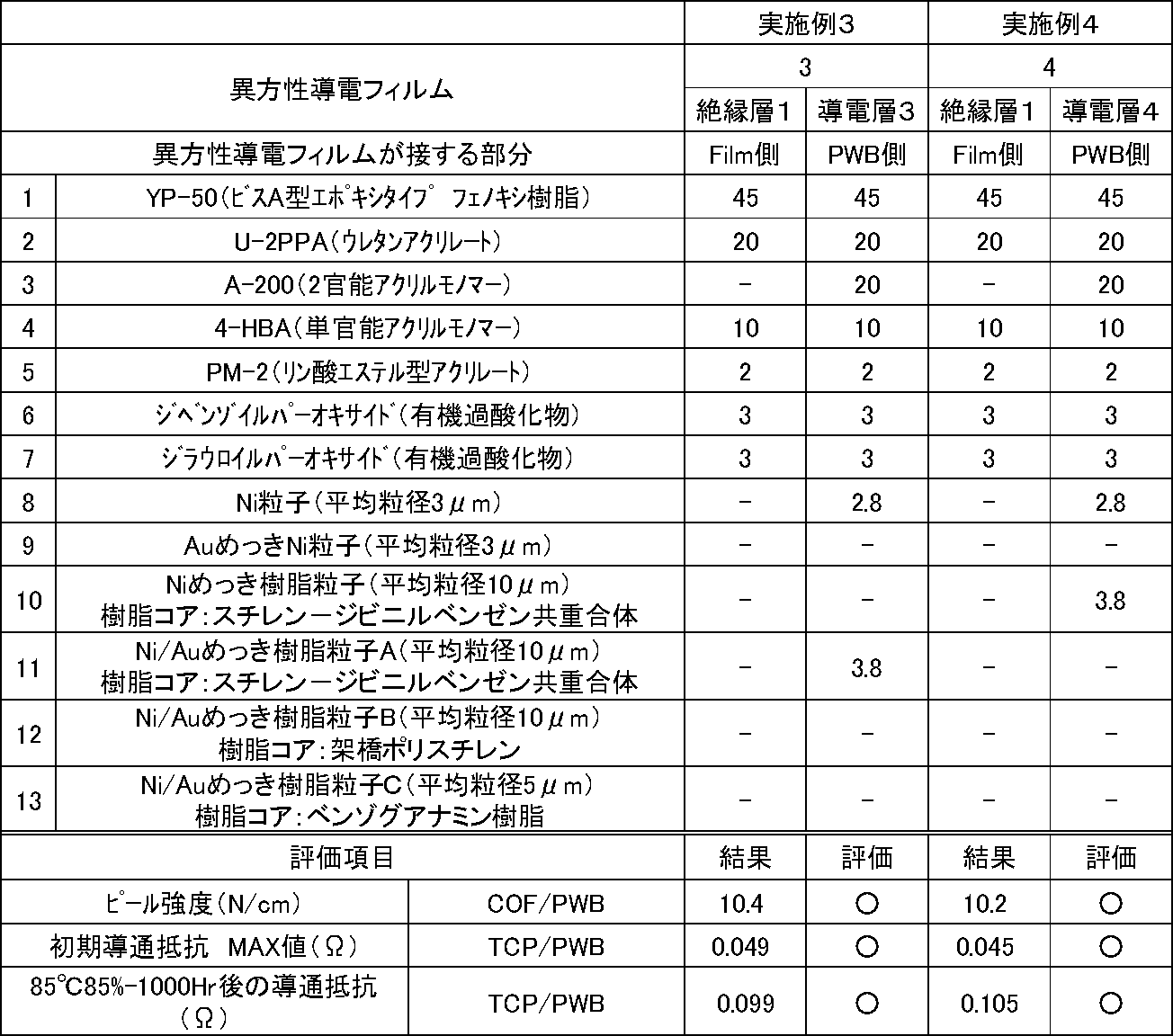
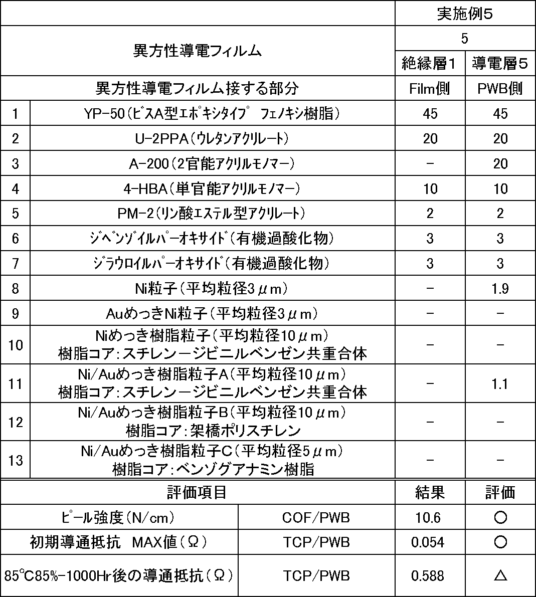
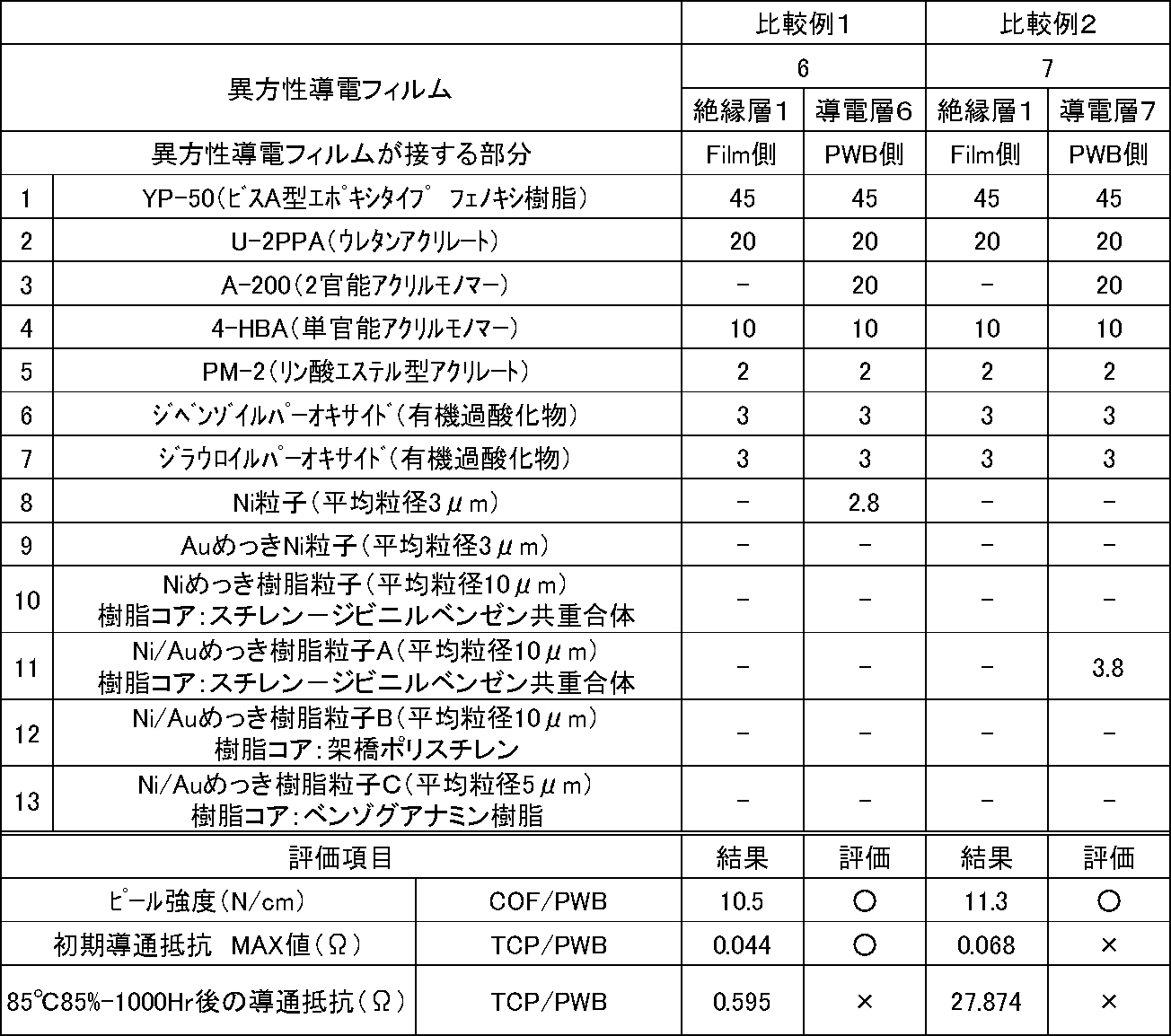
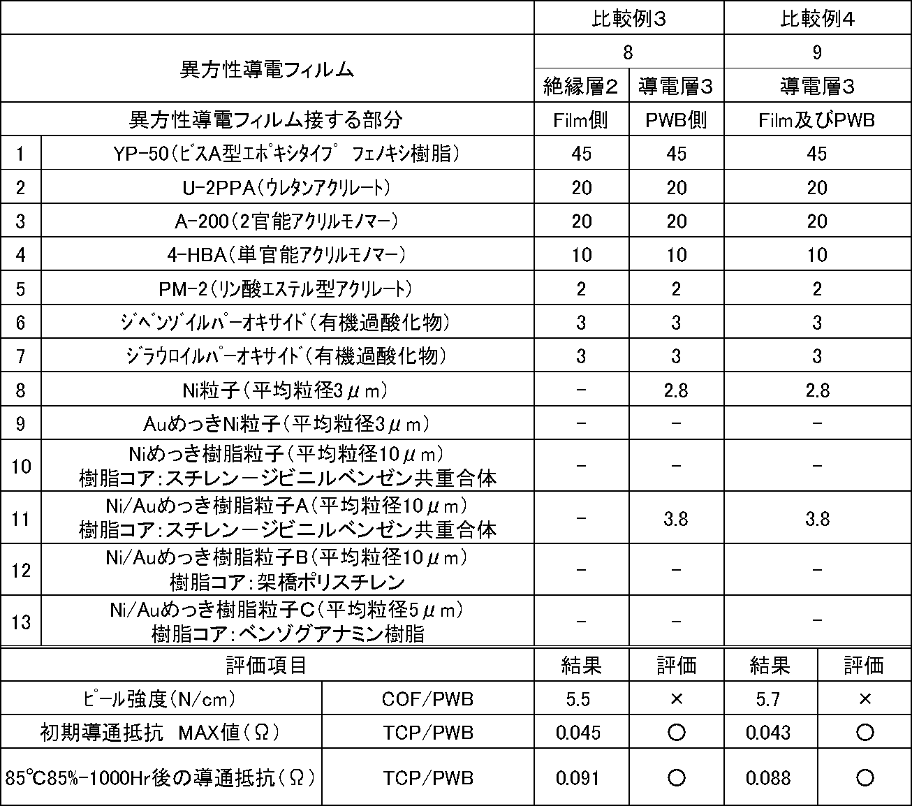

また、実施例1~5、及び比較例1、4、5は、いずれも初期導通抵抗が0.06Ω以下と低く、良好であった。
また、実施例3、4、及び比較例3、4は、いずれも高温高湿環境(85℃、85%RH)下で1,000時間後の導通抵抗が低く、良好であった。
また、実施例1は、導電層の金属被覆樹脂粒子の樹脂コアとして平均粒径が5μmのベンゾグアナミン樹脂を用いており、ピール強度及び初期導通抵抗は良好であるが、樹脂コア自体の反発力がスチレン-ジビニルベンゼン共重合体に比べ大きく、85℃、85%RH環境下では樹脂コアの反発力によりバインダー硬化物が緩んでしまうため、高温高湿環境(85℃、85%RH)下で1,000時間後の導通抵抗が若干高くなった。
また、実施例2は、導電層の金属被覆樹脂粒子の樹脂コアとして架橋ポリスチレンを用いており、ピール強度及び初期導通抵抗は良好であるが、架橋ポリスチレンは樹脂コア自体の反発力がスチレン-ジビニルベンゼン共重合体に比べて大きく、高温高湿環境(85℃、85%RH)下ではその反発力の影響で粒子を押さえつけているバインダー硬化物が緩んでしまい、結果として1,000時間後の導通抵抗が若干高くなった。
また、実施例3は、絶縁層に単官能アクリルモノマーを含み、導電層にNi粒子とNi/Auめっき樹脂粒子A(樹脂コア:スチレン-ジビニルベンゼン共重合体、平均粒径10μm)を含む本発明のベストモードである。
また、実施例4は、導電層の金属被覆樹脂粒子の樹脂コアとして柔らかいスチレン-ジビニルベンゼン共重合体を用いており、反発力が弱くなるため、粒子の潰れが良くなって粒子と電極の接触面積が大きくなり、Niめっきのみであっても、高温高湿環境(85℃で85%RH)下、1,000時間後でAu/Niめっきとあまり変わらないレベルの低い導通抵抗値が得られた。
また、実施例5は、Ni粒子とNi/Auめっき樹脂粒子Aの合計量が樹脂固形分100質量部に対し2.9質量部であり、実施例3のNi粒子とNi/Auめっき樹脂粒子Aの合計量が樹脂固形分100質量部に対し6.4質量部に比べて半分以下であるため、高温高湿環境(85℃、85%RH)下で1,000時間後の導通抵抗が高くなった。
これに対し、比較例1は、導電層にNi粒子のみを含むので、ピール強度及び初期導通抵抗は良好であるが、高温高湿環境(85℃、85%RH)下で1,000時間後の導通抵抗が高くなった。
また、比較例2は、導電層にNi粒子を含まず、Ni/Auめっき樹脂粒子Aを含むので、初期導通抵抗が、実施例3(ベストモード)よりも若干高く、高温高湿環境(85℃、85%RH)下で1,000時間後の導通抵抗は大きく上昇した。これは、Ni/Auめっき樹脂粒子AだけではPWBパターン表面に形成される酸化膜を突き破って導電性を得ることができないため、高温高湿環境(85℃、85%RH)下で1,000時間後に大きく上昇したと考えられる。
また、比較例3は、絶縁層に2官能アクリルモノマーを含むので、初期及び高温高湿環境(85℃、85%RH)下で1,000時間後の導通抵抗は良好であるが、ピール強度が低下してしまった。
また、比較例4は、導電層が単層であり、ピール強度が低下してしまった。
また、比較例5は、特開平11-339558号公報の実施例を再現したものであり、導電層が単層であり、硬化反応成分が単官能モノマーのみであるためバインダー硬化物のガラス転移温度(Tg)が低く(>85℃)、高温高湿環境(85℃で85%RH)下で樹脂コアの硬い粒子の反発力に負けてしまい、結果として1,000時間後の導通抵抗がOPENとなった。また、Ni粒子の外殻には柔らかいAuめっきがされているので、端子に食い込むことができず酸化膜を突き破ることも難しい。ただし、反応成分が単官能モノマーのみでガラス転移温度(Tg)が低くなるため、ピール強度は高い値を示した。
11 COF(第2の回路部材)
11a 端子
12 異方性導電フィルム
12a 導電性粒子(Ni粒子、少なくともNiで被覆した樹脂粒子)
20 剥離基材(セパレータ)
21 導電層
22 絶縁層
100 接合体
Claims (12)
- 少なくとも導電層と、絶縁層とを有してなり、
前記絶縁層が、バインダー、単官能の重合性モノマー、及び硬化剤を含有し、
前記導電層が、Ni粒子、金属被覆樹脂粒子、バインダー、重合性モノマー、及び硬化剤を含有し、
前記金属被覆樹脂粒子が、樹脂コアを少なくともNiで被覆した樹脂粒子であることを特徴とする異方性導電フィルム。 - 絶縁層が、フェノキシ樹脂、単官能の(メタ)アクリルモノマー、及び有機過酸化物を少なくとも含有する請求項1に記載の異方性導電フィルム。
- 導電層が、フェノキシ樹脂、(メタ)アクリルモノマー、及び有機過酸化物を少なくとも含有する請求項1から2のいずれかに記載の異方性導電フィルム。
- 金属被覆樹脂粒子が、樹脂コアをNiで被覆した樹脂粒子、及び樹脂コアをNiで被覆し、更に最表面をAuで被覆した樹脂粒子のいずれかである請求項1から3のいずれかに記載の異方性導電フィルム。
- 樹脂コアの材料が、スチレン-ジビニルベンゼン共重合体及びベンゾグアナミン樹脂のいずれかである請求項1から4のいずれかに記載の異方性導電フィルム。
- 金属被覆樹脂粒子の平均粒径が5μm以上である請求項1から5のいずれかに記載の異方性導電フィルム。
- Ni粒子及び金属被覆樹脂粒子の導電層における合計含有量が、導電層の樹脂固形分100質量部に対し3.0質量部~20質量部である請求項1から6のいずれかに記載の異方性導電フィルム。
- 第1の回路部材と、第2の回路部材と、請求項1から7のいずれかに記載の異方性導電フィルムと、を備え、
前記異方性導電フィルムを介して、前記第1の回路部材と前記第2の回路部材とが接合されていることを特徴とする接合体。 - 第1の回路部材が、プリント配線板であり、
第2の回路部材が、COFである請求項8に記載の接合体。 - 第1の回路部材と第2の回路部材との接続方法において、
請求項1から7のいずれかに記載の異方性導電フィルムが、前記第1の回路部材と第2の回路部材の間に挟持され、
前記第1の回路部材及び第2の回路部材から加熱しながら押圧することにより、前記異方性導電フィルムを硬化させて、前記第1の回路部材と前記第2の回路部材を接続することを特徴とする接続方法。 - 第1の回路部材が、プリント配線板であり、
第2の回路部材が、COFである請求項10に記載の接続方法。 - 異方性導電フィルムの導電層がプリント配線板側となり、前記異方性導電フィルムの絶縁層がCOF側になるように配置される請求項11に記載の接続方法。
Priority Applications (4)
| Application Number | Priority Date | Filing Date | Title |
|---|---|---|---|
| CN201180008066.XA CN102741943B (zh) | 2010-02-01 | 2011-01-20 | 异向性导电膜、接合体以及粘结方法 |
| KR1020157003087A KR20150023072A (ko) | 2010-02-01 | 2011-01-20 | 이방성 도전 필름, 접합체 및 접속 방법 |
| KR1020127022779A KR101640965B1 (ko) | 2010-02-01 | 2011-01-20 | 이방성 도전 필름, 접합체 및 접속 방법 |
| US13/534,667 US20120261171A1 (en) | 2010-02-01 | 2012-06-27 | Anisotropic conductive film, joined structure, and connecting method |
Applications Claiming Priority (2)
| Application Number | Priority Date | Filing Date | Title |
|---|---|---|---|
| JP2010-019974 | 2010-02-01 | ||
| JP2010019974A JP5833809B2 (ja) | 2010-02-01 | 2010-02-01 | 異方性導電フィルム、接合体及び接続方法 |
Related Child Applications (1)
| Application Number | Title | Priority Date | Filing Date |
|---|---|---|---|
| US13/534,667 Continuation US20120261171A1 (en) | 2010-02-01 | 2012-06-27 | Anisotropic conductive film, joined structure, and connecting method |
Publications (1)
| Publication Number | Publication Date |
|---|---|
| WO2011093207A1 true WO2011093207A1 (ja) | 2011-08-04 |
Family
ID=44319196
Family Applications (1)
| Application Number | Title | Priority Date | Filing Date |
|---|---|---|---|
| PCT/JP2011/051008 Ceased WO2011093207A1 (ja) | 2010-02-01 | 2011-01-20 | 異方性導電フィルム、接合体及び接続方法 |
Country Status (6)
| Country | Link |
|---|---|
| US (1) | US20120261171A1 (ja) |
| JP (1) | JP5833809B2 (ja) |
| KR (2) | KR20150023072A (ja) |
| CN (1) | CN102741943B (ja) |
| TW (1) | TWI540048B (ja) |
| WO (1) | WO2011093207A1 (ja) |
Cited By (2)
| Publication number | Priority date | Publication date | Assignee | Title |
|---|---|---|---|---|
| EP2791204A4 (en) * | 2011-12-13 | 2015-09-30 | Heraeus Precious Metals North America Conshohocken Llc | ELECTRICALLY CONDUCTIVE POLYMER COMPOSITIONS, CONTACTS AND ASSEMBLIES AND METHOD THEREFOR |
| CN106573424A (zh) * | 2014-04-08 | 2017-04-19 | 威廉马歇莱思大学 | 电子装置中的柔性导电膜和无机层的制作及用途 |
Families Citing this family (18)
| Publication number | Priority date | Publication date | Assignee | Title |
|---|---|---|---|---|
| JP5556488B2 (ja) * | 2010-08-06 | 2014-07-23 | デクセリアルズ株式会社 | 対向電極接続用接着剤 |
| WO2013042203A1 (ja) * | 2011-09-20 | 2013-03-28 | 日立化成株式会社 | 接着剤組成物、フィルム状接着剤、接着シート、回路接続体及び回路部材の接続方法 |
| KR101479658B1 (ko) * | 2011-11-18 | 2015-01-06 | 제일모직 주식회사 | 가압착 공정성이 개선된 이방성 도전 필름 |
| JP6218354B2 (ja) * | 2012-01-06 | 2017-10-25 | 積水化学工業株式会社 | 絶縁材料、多層フィルムの製造方法、積層体の製造方法、接続構造体及び接続構造体の製造方法 |
| JP5956362B2 (ja) * | 2013-02-19 | 2016-07-27 | デクセリアルズ株式会社 | 異方性導電フィルム、接続方法、及び接合体 |
| KR102125464B1 (ko) * | 2013-10-17 | 2020-06-23 | 삼성디스플레이 주식회사 | 이방성 도전 필름을 포함하는 표시 장치 및 이의 제조 방법 |
| KR101628440B1 (ko) * | 2013-10-31 | 2016-06-08 | 제일모직주식회사 | 이방성 도전 필름 및 이를 이용한 반도체 장치 |
| JP6280017B2 (ja) * | 2014-10-03 | 2018-02-14 | デクセリアルズ株式会社 | 異方性導電フィルム、並びに、接続方法及び接合体 |
| JP6457255B2 (ja) * | 2014-12-10 | 2019-01-23 | デクセリアルズ株式会社 | 接続体の検査方法、接続体、導電性粒子、異方性導電接着剤及び接続体の製造方法 |
| GB2539697A (en) * | 2015-06-25 | 2016-12-28 | Lussey David | Improved conductive polymer |
| KR101892341B1 (ko) | 2016-04-22 | 2018-08-27 | 삼성에스디아이 주식회사 | 이방성 도전 필름 |
| JP7039883B2 (ja) * | 2016-12-01 | 2022-03-23 | デクセリアルズ株式会社 | 異方性導電フィルム |
| KR101985499B1 (ko) * | 2017-12-28 | 2019-06-03 | 삼화콘덴서공업 주식회사 | 과전류 보호 기능을 가지는 금속 산화물 바리스터 |
| KR102469299B1 (ko) | 2018-01-03 | 2022-11-23 | 삼성디스플레이 주식회사 | 표시 장치 |
| JP7298256B2 (ja) * | 2019-04-11 | 2023-06-27 | 株式会社レゾナック | 導電粒子 |
| CN110358469A (zh) * | 2019-07-18 | 2019-10-22 | 业成科技(成都)有限公司 | 粘结组件及显示装置 |
| US11349053B1 (en) * | 2020-01-14 | 2022-05-31 | Facebook Technologies, Llc | Flexible interconnect using conductive adhesive |
| CN113903257A (zh) * | 2021-09-27 | 2022-01-07 | 业成科技(成都)有限公司 | 可拉伸电子模组及其应用的电子装置 |
Citations (2)
| Publication number | Priority date | Publication date | Assignee | Title |
|---|---|---|---|---|
| JP2001297631A (ja) * | 2000-04-13 | 2001-10-26 | Asahi Kasei Corp | 異方導電性フィルム |
| JP2009238635A (ja) * | 2008-03-27 | 2009-10-15 | Sony Chemical & Information Device Corp | 接合体及びその製造方法、並びに、異方性導電材料及びその製造方法 |
Family Cites Families (13)
| Publication number | Priority date | Publication date | Assignee | Title |
|---|---|---|---|---|
| JP3119230B2 (ja) * | 1998-03-03 | 2000-12-18 | 日本電気株式会社 | 樹脂フィルムおよびこれを用いた電子部品の接続方法 |
| JPH11339558A (ja) | 1998-05-26 | 1999-12-10 | Sekisui Chem Co Ltd | 異方性導電接着剤及び導電接続構造体 |
| JP4400674B2 (ja) * | 2002-02-28 | 2010-01-20 | 日立化成工業株式会社 | 回路接続材料及びそれを用いた回路端子の接続構造 |
| JP3940638B2 (ja) | 2002-06-10 | 2007-07-04 | 積水化学工業株式会社 | 導電性微粒子及び導電性微粒子の製造方法 |
| JP4188278B2 (ja) | 2004-05-06 | 2008-11-26 | 日本化学工業株式会社 | 異方導電性フィルムおよびヒートシールコネクター |
| JP2006233203A (ja) * | 2005-01-31 | 2006-09-07 | Asahi Kasei Electronics Co Ltd | 異方導電性接着剤フィルム |
| KR100720895B1 (ko) | 2005-07-05 | 2007-05-22 | 제일모직주식회사 | 농도 구배를 갖는 이종(異種) 복합 금속층이 형성된 전도성미립자, 그 제조방법 및 이를 이용한 이방 전도성 접착제조성물 |
| KR100719802B1 (ko) * | 2005-12-28 | 2007-05-18 | 제일모직주식회사 | 이방 전도 접속용 고신뢰성 전도성 미립자 |
| JP5033332B2 (ja) | 2006-02-09 | 2012-09-26 | ソニーケミカル&インフォメーションデバイス株式会社 | 異方導電性接着剤、異方導電性接着フィルム及び電極の接続方法 |
| JP2007242731A (ja) | 2006-03-06 | 2007-09-20 | Sekisui Chem Co Ltd | 接続構造体 |
| EP2134800A4 (en) * | 2007-03-16 | 2011-09-28 | 3M Innovative Properties Co | DICING- UDN THE-ATTACH-ADHESIVE |
| TWI389999B (zh) * | 2007-12-18 | 2013-03-21 | Cheil Ind Inc | 黏著性組成物及使用該黏著性組成物的各向異性導電膜 |
| JP5226562B2 (ja) * | 2008-03-27 | 2013-07-03 | デクセリアルズ株式会社 | 異方性導電フィルム、並びに、接合体及びその製造方法 |
-
2010
- 2010-02-01 JP JP2010019974A patent/JP5833809B2/ja active Active
-
2011
- 2011-01-20 KR KR1020157003087A patent/KR20150023072A/ko not_active Abandoned
- 2011-01-20 WO PCT/JP2011/051008 patent/WO2011093207A1/ja not_active Ceased
- 2011-01-20 CN CN201180008066.XA patent/CN102741943B/zh active Active
- 2011-01-20 KR KR1020127022779A patent/KR101640965B1/ko active Active
- 2011-01-28 TW TW100103367A patent/TWI540048B/zh active
-
2012
- 2012-06-27 US US13/534,667 patent/US20120261171A1/en not_active Abandoned
Patent Citations (2)
| Publication number | Priority date | Publication date | Assignee | Title |
|---|---|---|---|---|
| JP2001297631A (ja) * | 2000-04-13 | 2001-10-26 | Asahi Kasei Corp | 異方導電性フィルム |
| JP2009238635A (ja) * | 2008-03-27 | 2009-10-15 | Sony Chemical & Information Device Corp | 接合体及びその製造方法、並びに、異方性導電材料及びその製造方法 |
Cited By (2)
| Publication number | Priority date | Publication date | Assignee | Title |
|---|---|---|---|---|
| EP2791204A4 (en) * | 2011-12-13 | 2015-09-30 | Heraeus Precious Metals North America Conshohocken Llc | ELECTRICALLY CONDUCTIVE POLYMER COMPOSITIONS, CONTACTS AND ASSEMBLIES AND METHOD THEREFOR |
| CN106573424A (zh) * | 2014-04-08 | 2017-04-19 | 威廉马歇莱思大学 | 电子装置中的柔性导电膜和无机层的制作及用途 |
Also Published As
| Publication number | Publication date |
|---|---|
| JP5833809B2 (ja) | 2015-12-16 |
| CN102741943A (zh) | 2012-10-17 |
| US20120261171A1 (en) | 2012-10-18 |
| CN102741943B (zh) | 2016-02-10 |
| TW201136761A (en) | 2011-11-01 |
| KR20150023072A (ko) | 2015-03-04 |
| KR101640965B1 (ko) | 2016-07-19 |
| TWI540048B (zh) | 2016-07-01 |
| JP2011159486A (ja) | 2011-08-18 |
| KR20120124470A (ko) | 2012-11-13 |
Similar Documents
| Publication | Publication Date | Title |
|---|---|---|
| JP5833809B2 (ja) | 異方性導電フィルム、接合体及び接続方法 | |
| US8715833B2 (en) | Anisotropic conductive film | |
| CN101946371B (zh) | 连接膜、以及接合体及其制造方法 | |
| TWI628673B (zh) | Anisotropic conductive film, connection method, and connection structure | |
| CN101589514B (zh) | 各向异性导电膜 | |
| TWI655267B (zh) | Conductive adhesive and connection method of electronic parts | |
| KR20100100792A (ko) | 비전도성 접착제 조성물 및 필름 및 제조 방법 | |
| CN102782945A (zh) | 异向性导电膜、接合体以及接合体制造方法 | |
| JP5972564B2 (ja) | 接続方法、接続構造体、異方性導電フィルム及びその製造方法 | |
| US20120160539A1 (en) | Conductive adhesive tape | |
| JP6505423B2 (ja) | 実装体の製造方法、及び異方性導電フィルム | |
| JP5966069B2 (ja) | 異方性導電フィルム、接合体及び接続方法 | |
| KR102758192B1 (ko) | 접착제 조성물 | |
| TW201834858A (zh) | 異向性導電連接構造體、異向性導電連接構造體之製造方法、異向性導電膜、及異向性導電糊 | |
| JP4363844B2 (ja) | 低温硬化型接着剤及びこれを用いた異方導電性接着フィルム | |
| JP6286473B2 (ja) | 接合体 | |
| JP5924896B2 (ja) | 接合体の製造方法 | |
| HK1177321A (en) | Anisotropic conductive film, bonded body and bonding method | |
| WO2024116988A1 (ja) | 異方性導電フィルム、接続構造体および接続構造体の製造方法 | |
| WO2015133211A1 (ja) | 接続構造体、接続構造体の製造方法、及び回路接続材料 |
Legal Events
| Date | Code | Title | Description |
|---|---|---|---|
| WWE | Wipo information: entry into national phase |
Ref document number: 201180008066.X Country of ref document: CN |
|
| 121 | Ep: the epo has been informed by wipo that ep was designated in this application |
Ref document number: 11736921 Country of ref document: EP Kind code of ref document: A1 |
|
| NENP | Non-entry into the national phase |
Ref country code: DE |
|
| ENP | Entry into the national phase |
Ref document number: 20127022779 Country of ref document: KR Kind code of ref document: A |
|
| 122 | Ep: pct application non-entry in european phase |
Ref document number: 11736921 Country of ref document: EP Kind code of ref document: A1 |