WO2011093162A1 - Conductive connection sheet, method for connecting terminals, method for forming connection terminal, semiconductor device, and electronic device - Google Patents
Conductive connection sheet, method for connecting terminals, method for forming connection terminal, semiconductor device, and electronic device Download PDFInfo
- Publication number
- WO2011093162A1 WO2011093162A1 PCT/JP2011/050684 JP2011050684W WO2011093162A1 WO 2011093162 A1 WO2011093162 A1 WO 2011093162A1 JP 2011050684 W JP2011050684 W JP 2011050684W WO 2011093162 A1 WO2011093162 A1 WO 2011093162A1
- Authority
- WO
- WIPO (PCT)
- Prior art keywords
- resin composition
- conductive connection
- connection sheet
- terminals
- layer
- Prior art date
Links
Images


Classifications
-
- H—ELECTRICITY
- H01—ELECTRIC ELEMENTS
- H01L—SEMICONDUCTOR DEVICES NOT COVERED BY CLASS H10
- H01L24/00—Arrangements for connecting or disconnecting semiconductor or solid-state bodies; Methods or apparatus related thereto
- H01L24/01—Means for bonding being attached to, or being formed on, the surface to be connected, e.g. chip-to-package, die-attach, "first-level" interconnects; Manufacturing methods related thereto
- H01L24/26—Layer connectors, e.g. plate connectors, solder or adhesive layers; Manufacturing methods related thereto
- H01L24/28—Structure, shape, material or disposition of the layer connectors prior to the connecting process
- H01L24/29—Structure, shape, material or disposition of the layer connectors prior to the connecting process of an individual layer connector
-
- B—PERFORMING OPERATIONS; TRANSPORTING
- B32—LAYERED PRODUCTS
- B32B—LAYERED PRODUCTS, i.e. PRODUCTS BUILT-UP OF STRATA OF FLAT OR NON-FLAT, e.g. CELLULAR OR HONEYCOMB, FORM
- B32B15/00—Layered products comprising a layer of metal
- B32B15/04—Layered products comprising a layer of metal comprising metal as the main or only constituent of a layer, which is next to another layer of the same or of a different material
- B32B15/08—Layered products comprising a layer of metal comprising metal as the main or only constituent of a layer, which is next to another layer of the same or of a different material of synthetic resin
-
- C—CHEMISTRY; METALLURGY
- C09—DYES; PAINTS; POLISHES; NATURAL RESINS; ADHESIVES; COMPOSITIONS NOT OTHERWISE PROVIDED FOR; APPLICATIONS OF MATERIALS NOT OTHERWISE PROVIDED FOR
- C09D—COATING COMPOSITIONS, e.g. PAINTS, VARNISHES OR LACQUERS; FILLING PASTES; CHEMICAL PAINT OR INK REMOVERS; INKS; CORRECTING FLUIDS; WOODSTAINS; PASTES OR SOLIDS FOR COLOURING OR PRINTING; USE OF MATERIALS THEREFOR
- C09D5/00—Coating compositions, e.g. paints, varnishes or lacquers, characterised by their physical nature or the effects produced; Filling pastes
- C09D5/24—Electrically-conducting paints
-
- H—ELECTRICITY
- H01—ELECTRIC ELEMENTS
- H01L—SEMICONDUCTOR DEVICES NOT COVERED BY CLASS H10
- H01L23/00—Details of semiconductor or other solid state devices
- H01L23/48—Arrangements for conducting electric current to or from the solid state body in operation, e.g. leads, terminal arrangements ; Selection of materials therefor
- H01L23/488—Arrangements for conducting electric current to or from the solid state body in operation, e.g. leads, terminal arrangements ; Selection of materials therefor consisting of soldered or bonded constructions
- H01L23/498—Leads, i.e. metallisations or lead-frames on insulating substrates, e.g. chip carriers
- H01L23/49811—Additional leads joined to the metallisation on the insulating substrate, e.g. pins, bumps, wires, flat leads
-
- H—ELECTRICITY
- H01—ELECTRIC ELEMENTS
- H01L—SEMICONDUCTOR DEVICES NOT COVERED BY CLASS H10
- H01L24/00—Arrangements for connecting or disconnecting semiconductor or solid-state bodies; Methods or apparatus related thereto
- H01L24/01—Means for bonding being attached to, or being formed on, the surface to be connected, e.g. chip-to-package, die-attach, "first-level" interconnects; Manufacturing methods related thereto
- H01L24/10—Bump connectors ; Manufacturing methods related thereto
- H01L24/11—Manufacturing methods
-
- H—ELECTRICITY
- H01—ELECTRIC ELEMENTS
- H01L—SEMICONDUCTOR DEVICES NOT COVERED BY CLASS H10
- H01L24/00—Arrangements for connecting or disconnecting semiconductor or solid-state bodies; Methods or apparatus related thereto
- H01L24/01—Means for bonding being attached to, or being formed on, the surface to be connected, e.g. chip-to-package, die-attach, "first-level" interconnects; Manufacturing methods related thereto
- H01L24/10—Bump connectors ; Manufacturing methods related thereto
- H01L24/15—Structure, shape, material or disposition of the bump connectors after the connecting process
- H01L24/16—Structure, shape, material or disposition of the bump connectors after the connecting process of an individual bump connector
-
- H—ELECTRICITY
- H01—ELECTRIC ELEMENTS
- H01L—SEMICONDUCTOR DEVICES NOT COVERED BY CLASS H10
- H01L24/00—Arrangements for connecting or disconnecting semiconductor or solid-state bodies; Methods or apparatus related thereto
- H01L24/01—Means for bonding being attached to, or being formed on, the surface to be connected, e.g. chip-to-package, die-attach, "first-level" interconnects; Manufacturing methods related thereto
- H01L24/26—Layer connectors, e.g. plate connectors, solder or adhesive layers; Manufacturing methods related thereto
- H01L24/31—Structure, shape, material or disposition of the layer connectors after the connecting process
- H01L24/32—Structure, shape, material or disposition of the layer connectors after the connecting process of an individual layer connector
-
- H—ELECTRICITY
- H01—ELECTRIC ELEMENTS
- H01L—SEMICONDUCTOR DEVICES NOT COVERED BY CLASS H10
- H01L24/00—Arrangements for connecting or disconnecting semiconductor or solid-state bodies; Methods or apparatus related thereto
- H01L24/80—Methods for connecting semiconductor or other solid state bodies using means for bonding being attached to, or being formed on, the surface to be connected
- H01L24/81—Methods for connecting semiconductor or other solid state bodies using means for bonding being attached to, or being formed on, the surface to be connected using a bump connector
-
- H—ELECTRICITY
- H05—ELECTRIC TECHNIQUES NOT OTHERWISE PROVIDED FOR
- H05K—PRINTED CIRCUITS; CASINGS OR CONSTRUCTIONAL DETAILS OF ELECTRIC APPARATUS; MANUFACTURE OF ASSEMBLAGES OF ELECTRICAL COMPONENTS
- H05K3/00—Apparatus or processes for manufacturing printed circuits
- H05K3/30—Assembling printed circuits with electric components, e.g. with resistor
- H05K3/32—Assembling printed circuits with electric components, e.g. with resistor electrically connecting electric components or wires to printed circuits
- H05K3/34—Assembling printed circuits with electric components, e.g. with resistor electrically connecting electric components or wires to printed circuits by soldering
- H05K3/341—Surface mounted components
- H05K3/3431—Leadless components
- H05K3/3436—Leadless components having an array of bottom contacts, e.g. pad grid array or ball grid array components
-
- H—ELECTRICITY
- H05—ELECTRIC TECHNIQUES NOT OTHERWISE PROVIDED FOR
- H05K—PRINTED CIRCUITS; CASINGS OR CONSTRUCTIONAL DETAILS OF ELECTRIC APPARATUS; MANUFACTURE OF ASSEMBLAGES OF ELECTRICAL COMPONENTS
- H05K3/00—Apparatus or processes for manufacturing printed circuits
- H05K3/30—Assembling printed circuits with electric components, e.g. with resistor
- H05K3/32—Assembling printed circuits with electric components, e.g. with resistor electrically connecting electric components or wires to printed circuits
- H05K3/34—Assembling printed circuits with electric components, e.g. with resistor electrically connecting electric components or wires to printed circuits by soldering
- H05K3/3457—Solder materials or compositions; Methods of application thereof
- H05K3/3478—Applying solder preforms; Transferring prefabricated solder patterns
-
- B—PERFORMING OPERATIONS; TRANSPORTING
- B32—LAYERED PRODUCTS
- B32B—LAYERED PRODUCTS, i.e. PRODUCTS BUILT-UP OF STRATA OF FLAT OR NON-FLAT, e.g. CELLULAR OR HONEYCOMB, FORM
- B32B2311/00—Metals, their alloys or their compounds
- B32B2311/14—Lead
-
- B—PERFORMING OPERATIONS; TRANSPORTING
- B32—LAYERED PRODUCTS
- B32B—LAYERED PRODUCTS, i.e. PRODUCTS BUILT-UP OF STRATA OF FLAT OR NON-FLAT, e.g. CELLULAR OR HONEYCOMB, FORM
- B32B2311/00—Metals, their alloys or their compounds
- B32B2311/16—Tin
-
- H—ELECTRICITY
- H01—ELECTRIC ELEMENTS
- H01L—SEMICONDUCTOR DEVICES NOT COVERED BY CLASS H10
- H01L2224/00—Indexing scheme for arrangements for connecting or disconnecting semiconductor or solid-state bodies and methods related thereto as covered by H01L24/00
- H01L2224/01—Means for bonding being attached to, or being formed on, the surface to be connected, e.g. chip-to-package, die-attach, "first-level" interconnects; Manufacturing methods related thereto
- H01L2224/10—Bump connectors; Manufacturing methods related thereto
- H01L2224/11—Manufacturing methods
- H01L2224/114—Manufacturing methods by blanket deposition of the material of the bump connector
- H01L2224/1143—Manufacturing methods by blanket deposition of the material of the bump connector in solid form
- H01L2224/11436—Lamination of a preform, e.g. foil, sheet or layer
-
- H—ELECTRICITY
- H01—ELECTRIC ELEMENTS
- H01L—SEMICONDUCTOR DEVICES NOT COVERED BY CLASS H10
- H01L2224/00—Indexing scheme for arrangements for connecting or disconnecting semiconductor or solid-state bodies and methods related thereto as covered by H01L24/00
- H01L2224/01—Means for bonding being attached to, or being formed on, the surface to be connected, e.g. chip-to-package, die-attach, "first-level" interconnects; Manufacturing methods related thereto
- H01L2224/10—Bump connectors; Manufacturing methods related thereto
- H01L2224/11—Manufacturing methods
- H01L2224/115—Manufacturing methods by chemical or physical modification of a pre-existing or pre-deposited material
- H01L2224/1152—Self-assembly, e.g. self-agglomeration of the bump material in a fluid
- H01L2224/11522—Auxiliary means therefor, e.g. for self-assembly activation
-
- H—ELECTRICITY
- H01—ELECTRIC ELEMENTS
- H01L—SEMICONDUCTOR DEVICES NOT COVERED BY CLASS H10
- H01L2224/00—Indexing scheme for arrangements for connecting or disconnecting semiconductor or solid-state bodies and methods related thereto as covered by H01L24/00
- H01L2224/01—Means for bonding being attached to, or being formed on, the surface to be connected, e.g. chip-to-package, die-attach, "first-level" interconnects; Manufacturing methods related thereto
- H01L2224/10—Bump connectors; Manufacturing methods related thereto
- H01L2224/12—Structure, shape, material or disposition of the bump connectors prior to the connecting process
- H01L2224/13—Structure, shape, material or disposition of the bump connectors prior to the connecting process of an individual bump connector
- H01L2224/13001—Core members of the bump connector
- H01L2224/1302—Disposition
- H01L2224/13022—Disposition the bump connector being at least partially embedded in the surface
-
- H—ELECTRICITY
- H01—ELECTRIC ELEMENTS
- H01L—SEMICONDUCTOR DEVICES NOT COVERED BY CLASS H10
- H01L2224/00—Indexing scheme for arrangements for connecting or disconnecting semiconductor or solid-state bodies and methods related thereto as covered by H01L24/00
- H01L2224/01—Means for bonding being attached to, or being formed on, the surface to be connected, e.g. chip-to-package, die-attach, "first-level" interconnects; Manufacturing methods related thereto
- H01L2224/10—Bump connectors; Manufacturing methods related thereto
- H01L2224/12—Structure, shape, material or disposition of the bump connectors prior to the connecting process
- H01L2224/13—Structure, shape, material or disposition of the bump connectors prior to the connecting process of an individual bump connector
- H01L2224/13001—Core members of the bump connector
- H01L2224/13099—Material
- H01L2224/131—Material with a principal constituent of the material being a metal or a metalloid, e.g. boron [B], silicon [Si], germanium [Ge], arsenic [As], antimony [Sb], tellurium [Te] and polonium [Po], and alloys thereof
- H01L2224/13101—Material with a principal constituent of the material being a metal or a metalloid, e.g. boron [B], silicon [Si], germanium [Ge], arsenic [As], antimony [Sb], tellurium [Te] and polonium [Po], and alloys thereof the principal constituent melting at a temperature of less than 400°C
- H01L2224/13111—Tin [Sn] as principal constituent
-
- H—ELECTRICITY
- H01—ELECTRIC ELEMENTS
- H01L—SEMICONDUCTOR DEVICES NOT COVERED BY CLASS H10
- H01L2224/00—Indexing scheme for arrangements for connecting or disconnecting semiconductor or solid-state bodies and methods related thereto as covered by H01L24/00
- H01L2224/01—Means for bonding being attached to, or being formed on, the surface to be connected, e.g. chip-to-package, die-attach, "first-level" interconnects; Manufacturing methods related thereto
- H01L2224/10—Bump connectors; Manufacturing methods related thereto
- H01L2224/15—Structure, shape, material or disposition of the bump connectors after the connecting process
- H01L2224/16—Structure, shape, material or disposition of the bump connectors after the connecting process of an individual bump connector
- H01L2224/161—Disposition
- H01L2224/16151—Disposition the bump connector connecting between a semiconductor or solid-state body and an item not being a semiconductor or solid-state body, e.g. chip-to-substrate, chip-to-passive
- H01L2224/16221—Disposition the bump connector connecting between a semiconductor or solid-state body and an item not being a semiconductor or solid-state body, e.g. chip-to-substrate, chip-to-passive the body and the item being stacked
- H01L2224/16225—Disposition the bump connector connecting between a semiconductor or solid-state body and an item not being a semiconductor or solid-state body, e.g. chip-to-substrate, chip-to-passive the body and the item being stacked the item being non-metallic, e.g. insulating substrate with or without metallisation
-
- H—ELECTRICITY
- H01—ELECTRIC ELEMENTS
- H01L—SEMICONDUCTOR DEVICES NOT COVERED BY CLASS H10
- H01L2224/00—Indexing scheme for arrangements for connecting or disconnecting semiconductor or solid-state bodies and methods related thereto as covered by H01L24/00
- H01L2224/01—Means for bonding being attached to, or being formed on, the surface to be connected, e.g. chip-to-package, die-attach, "first-level" interconnects; Manufacturing methods related thereto
- H01L2224/26—Layer connectors, e.g. plate connectors, solder or adhesive layers; Manufacturing methods related thereto
- H01L2224/28—Structure, shape, material or disposition of the layer connectors prior to the connecting process
- H01L2224/29—Structure, shape, material or disposition of the layer connectors prior to the connecting process of an individual layer connector
- H01L2224/29001—Core members of the layer connector
- H01L2224/2901—Shape
- H01L2224/29012—Shape in top view
-
- H—ELECTRICITY
- H01—ELECTRIC ELEMENTS
- H01L—SEMICONDUCTOR DEVICES NOT COVERED BY CLASS H10
- H01L2224/00—Indexing scheme for arrangements for connecting or disconnecting semiconductor or solid-state bodies and methods related thereto as covered by H01L24/00
- H01L2224/01—Means for bonding being attached to, or being formed on, the surface to be connected, e.g. chip-to-package, die-attach, "first-level" interconnects; Manufacturing methods related thereto
- H01L2224/26—Layer connectors, e.g. plate connectors, solder or adhesive layers; Manufacturing methods related thereto
- H01L2224/28—Structure, shape, material or disposition of the layer connectors prior to the connecting process
- H01L2224/29—Structure, shape, material or disposition of the layer connectors prior to the connecting process of an individual layer connector
- H01L2224/29001—Core members of the layer connector
- H01L2224/29099—Material
- H01L2224/291—Material with a principal constituent of the material being a metal or a metalloid, e.g. boron [B], silicon [Si], germanium [Ge], arsenic [As], antimony [Sb], tellurium [Te] and polonium [Po], and alloys thereof
- H01L2224/29101—Material with a principal constituent of the material being a metal or a metalloid, e.g. boron [B], silicon [Si], germanium [Ge], arsenic [As], antimony [Sb], tellurium [Te] and polonium [Po], and alloys thereof the principal constituent melting at a temperature of less than 400°C
- H01L2224/29109—Indium [In] as principal constituent
-
- H—ELECTRICITY
- H01—ELECTRIC ELEMENTS
- H01L—SEMICONDUCTOR DEVICES NOT COVERED BY CLASS H10
- H01L2224/00—Indexing scheme for arrangements for connecting or disconnecting semiconductor or solid-state bodies and methods related thereto as covered by H01L24/00
- H01L2224/01—Means for bonding being attached to, or being formed on, the surface to be connected, e.g. chip-to-package, die-attach, "first-level" interconnects; Manufacturing methods related thereto
- H01L2224/26—Layer connectors, e.g. plate connectors, solder or adhesive layers; Manufacturing methods related thereto
- H01L2224/28—Structure, shape, material or disposition of the layer connectors prior to the connecting process
- H01L2224/29—Structure, shape, material or disposition of the layer connectors prior to the connecting process of an individual layer connector
- H01L2224/29001—Core members of the layer connector
- H01L2224/29099—Material
- H01L2224/291—Material with a principal constituent of the material being a metal or a metalloid, e.g. boron [B], silicon [Si], germanium [Ge], arsenic [As], antimony [Sb], tellurium [Te] and polonium [Po], and alloys thereof
- H01L2224/29101—Material with a principal constituent of the material being a metal or a metalloid, e.g. boron [B], silicon [Si], germanium [Ge], arsenic [As], antimony [Sb], tellurium [Te] and polonium [Po], and alloys thereof the principal constituent melting at a temperature of less than 400°C
- H01L2224/29111—Tin [Sn] as principal constituent
-
- H—ELECTRICITY
- H01—ELECTRIC ELEMENTS
- H01L—SEMICONDUCTOR DEVICES NOT COVERED BY CLASS H10
- H01L2224/00—Indexing scheme for arrangements for connecting or disconnecting semiconductor or solid-state bodies and methods related thereto as covered by H01L24/00
- H01L2224/01—Means for bonding being attached to, or being formed on, the surface to be connected, e.g. chip-to-package, die-attach, "first-level" interconnects; Manufacturing methods related thereto
- H01L2224/26—Layer connectors, e.g. plate connectors, solder or adhesive layers; Manufacturing methods related thereto
- H01L2224/28—Structure, shape, material or disposition of the layer connectors prior to the connecting process
- H01L2224/29—Structure, shape, material or disposition of the layer connectors prior to the connecting process of an individual layer connector
- H01L2224/29001—Core members of the layer connector
- H01L2224/29099—Material
- H01L2224/2919—Material with a principal constituent of the material being a polymer, e.g. polyester, phenolic based polymer, epoxy
-
- H—ELECTRICITY
- H01—ELECTRIC ELEMENTS
- H01L—SEMICONDUCTOR DEVICES NOT COVERED BY CLASS H10
- H01L2224/00—Indexing scheme for arrangements for connecting or disconnecting semiconductor or solid-state bodies and methods related thereto as covered by H01L24/00
- H01L2224/01—Means for bonding being attached to, or being formed on, the surface to be connected, e.g. chip-to-package, die-attach, "first-level" interconnects; Manufacturing methods related thereto
- H01L2224/26—Layer connectors, e.g. plate connectors, solder or adhesive layers; Manufacturing methods related thereto
- H01L2224/28—Structure, shape, material or disposition of the layer connectors prior to the connecting process
- H01L2224/29—Structure, shape, material or disposition of the layer connectors prior to the connecting process of an individual layer connector
- H01L2224/29001—Core members of the layer connector
- H01L2224/29099—Material
- H01L2224/29198—Material with a principal constituent of the material being a combination of two or more materials in the form of a matrix with a filler, i.e. being a hybrid material, e.g. segmented structures, foams
- H01L2224/29199—Material of the matrix
- H01L2224/2929—Material of the matrix with a principal constituent of the material being a polymer, e.g. polyester, phenolic based polymer, epoxy
-
- H—ELECTRICITY
- H01—ELECTRIC ELEMENTS
- H01L—SEMICONDUCTOR DEVICES NOT COVERED BY CLASS H10
- H01L2224/00—Indexing scheme for arrangements for connecting or disconnecting semiconductor or solid-state bodies and methods related thereto as covered by H01L24/00
- H01L2224/01—Means for bonding being attached to, or being formed on, the surface to be connected, e.g. chip-to-package, die-attach, "first-level" interconnects; Manufacturing methods related thereto
- H01L2224/26—Layer connectors, e.g. plate connectors, solder or adhesive layers; Manufacturing methods related thereto
- H01L2224/28—Structure, shape, material or disposition of the layer connectors prior to the connecting process
- H01L2224/29—Structure, shape, material or disposition of the layer connectors prior to the connecting process of an individual layer connector
- H01L2224/29001—Core members of the layer connector
- H01L2224/29099—Material
- H01L2224/29198—Material with a principal constituent of the material being a combination of two or more materials in the form of a matrix with a filler, i.e. being a hybrid material, e.g. segmented structures, foams
- H01L2224/29298—Fillers
- H01L2224/29299—Base material
- H01L2224/293—Base material with a principal constituent of the material being a metal or a metalloid, e.g. boron [B], silicon [Si], germanium [Ge], arsenic [As], antimony [Sb], tellurium [Te] and polonium [Po], and alloys thereof
- H01L2224/29301—Base material with a principal constituent of the material being a metal or a metalloid, e.g. boron [B], silicon [Si], germanium [Ge], arsenic [As], antimony [Sb], tellurium [Te] and polonium [Po], and alloys thereof the principal constituent melting at a temperature of less than 400°C
- H01L2224/29311—Tin [Sn] as principal constituent
-
- H—ELECTRICITY
- H01—ELECTRIC ELEMENTS
- H01L—SEMICONDUCTOR DEVICES NOT COVERED BY CLASS H10
- H01L2224/00—Indexing scheme for arrangements for connecting or disconnecting semiconductor or solid-state bodies and methods related thereto as covered by H01L24/00
- H01L2224/01—Means for bonding being attached to, or being formed on, the surface to be connected, e.g. chip-to-package, die-attach, "first-level" interconnects; Manufacturing methods related thereto
- H01L2224/26—Layer connectors, e.g. plate connectors, solder or adhesive layers; Manufacturing methods related thereto
- H01L2224/31—Structure, shape, material or disposition of the layer connectors after the connecting process
- H01L2224/32—Structure, shape, material or disposition of the layer connectors after the connecting process of an individual layer connector
- H01L2224/321—Disposition
- H01L2224/32151—Disposition the layer connector connecting between a semiconductor or solid-state body and an item not being a semiconductor or solid-state body, e.g. chip-to-substrate, chip-to-passive
- H01L2224/32221—Disposition the layer connector connecting between a semiconductor or solid-state body and an item not being a semiconductor or solid-state body, e.g. chip-to-substrate, chip-to-passive the body and the item being stacked
- H01L2224/32225—Disposition the layer connector connecting between a semiconductor or solid-state body and an item not being a semiconductor or solid-state body, e.g. chip-to-substrate, chip-to-passive the body and the item being stacked the item being non-metallic, e.g. insulating substrate with or without metallisation
-
- H—ELECTRICITY
- H01—ELECTRIC ELEMENTS
- H01L—SEMICONDUCTOR DEVICES NOT COVERED BY CLASS H10
- H01L2224/00—Indexing scheme for arrangements for connecting or disconnecting semiconductor or solid-state bodies and methods related thereto as covered by H01L24/00
- H01L2224/73—Means for bonding being of different types provided for in two or more of groups H01L2224/10, H01L2224/18, H01L2224/26, H01L2224/34, H01L2224/42, H01L2224/50, H01L2224/63, H01L2224/71
- H01L2224/732—Location after the connecting process
- H01L2224/73201—Location after the connecting process on the same surface
- H01L2224/73203—Bump and layer connectors
- H01L2224/73204—Bump and layer connectors the bump connector being embedded into the layer connector
-
- H—ELECTRICITY
- H01—ELECTRIC ELEMENTS
- H01L—SEMICONDUCTOR DEVICES NOT COVERED BY CLASS H10
- H01L2224/00—Indexing scheme for arrangements for connecting or disconnecting semiconductor or solid-state bodies and methods related thereto as covered by H01L24/00
- H01L2224/80—Methods for connecting semiconductor or other solid state bodies using means for bonding being attached to, or being formed on, the surface to be connected
- H01L2224/83—Methods for connecting semiconductor or other solid state bodies using means for bonding being attached to, or being formed on, the surface to be connected using a layer connector
- H01L2224/831—Methods for connecting semiconductor or other solid state bodies using means for bonding being attached to, or being formed on, the surface to be connected using a layer connector the layer connector being supplied to the parts to be connected in the bonding apparatus
- H01L2224/83101—Methods for connecting semiconductor or other solid state bodies using means for bonding being attached to, or being formed on, the surface to be connected using a layer connector the layer connector being supplied to the parts to be connected in the bonding apparatus as prepeg comprising a layer connector, e.g. provided in an insulating plate member
-
- H—ELECTRICITY
- H01—ELECTRIC ELEMENTS
- H01L—SEMICONDUCTOR DEVICES NOT COVERED BY CLASS H10
- H01L2224/00—Indexing scheme for arrangements for connecting or disconnecting semiconductor or solid-state bodies and methods related thereto as covered by H01L24/00
- H01L2224/80—Methods for connecting semiconductor or other solid state bodies using means for bonding being attached to, or being formed on, the surface to be connected
- H01L2224/83—Methods for connecting semiconductor or other solid state bodies using means for bonding being attached to, or being formed on, the surface to be connected using a layer connector
- H01L2224/832—Applying energy for connecting
- H01L2224/83201—Compression bonding
- H01L2224/83203—Thermocompression bonding, e.g. diffusion bonding, pressure joining, thermocompression welding or solid-state welding
-
- H—ELECTRICITY
- H01—ELECTRIC ELEMENTS
- H01L—SEMICONDUCTOR DEVICES NOT COVERED BY CLASS H10
- H01L2224/00—Indexing scheme for arrangements for connecting or disconnecting semiconductor or solid-state bodies and methods related thereto as covered by H01L24/00
- H01L2224/80—Methods for connecting semiconductor or other solid state bodies using means for bonding being attached to, or being formed on, the surface to be connected
- H01L2224/83—Methods for connecting semiconductor or other solid state bodies using means for bonding being attached to, or being formed on, the surface to be connected using a layer connector
- H01L2224/832—Applying energy for connecting
- H01L2224/83201—Compression bonding
- H01L2224/83205—Ultrasonic bonding
-
- H—ELECTRICITY
- H01—ELECTRIC ELEMENTS
- H01L—SEMICONDUCTOR DEVICES NOT COVERED BY CLASS H10
- H01L2224/00—Indexing scheme for arrangements for connecting or disconnecting semiconductor or solid-state bodies and methods related thereto as covered by H01L24/00
- H01L2224/80—Methods for connecting semiconductor or other solid state bodies using means for bonding being attached to, or being formed on, the surface to be connected
- H01L2224/83—Methods for connecting semiconductor or other solid state bodies using means for bonding being attached to, or being formed on, the surface to be connected using a layer connector
- H01L2224/832—Applying energy for connecting
- H01L2224/8322—Applying energy for connecting with energy being in the form of electromagnetic radiation
- H01L2224/83222—Induction heating, i.e. eddy currents
-
- H—ELECTRICITY
- H01—ELECTRIC ELEMENTS
- H01L—SEMICONDUCTOR DEVICES NOT COVERED BY CLASS H10
- H01L2224/00—Indexing scheme for arrangements for connecting or disconnecting semiconductor or solid-state bodies and methods related thereto as covered by H01L24/00
- H01L2224/80—Methods for connecting semiconductor or other solid state bodies using means for bonding being attached to, or being formed on, the surface to be connected
- H01L2224/83—Methods for connecting semiconductor or other solid state bodies using means for bonding being attached to, or being formed on, the surface to be connected using a layer connector
- H01L2224/832—Applying energy for connecting
- H01L2224/8322—Applying energy for connecting with energy being in the form of electromagnetic radiation
- H01L2224/83224—Applying energy for connecting with energy being in the form of electromagnetic radiation using a laser
-
- H—ELECTRICITY
- H01—ELECTRIC ELEMENTS
- H01L—SEMICONDUCTOR DEVICES NOT COVERED BY CLASS H10
- H01L2224/00—Indexing scheme for arrangements for connecting or disconnecting semiconductor or solid-state bodies and methods related thereto as covered by H01L24/00
- H01L2224/80—Methods for connecting semiconductor or other solid state bodies using means for bonding being attached to, or being formed on, the surface to be connected
- H01L2224/83—Methods for connecting semiconductor or other solid state bodies using means for bonding being attached to, or being formed on, the surface to be connected using a layer connector
- H01L2224/838—Bonding techniques
- H01L2224/83801—Soldering or alloying
- H01L2224/83815—Reflow soldering
-
- H—ELECTRICITY
- H01—ELECTRIC ELEMENTS
- H01L—SEMICONDUCTOR DEVICES NOT COVERED BY CLASS H10
- H01L2224/00—Indexing scheme for arrangements for connecting or disconnecting semiconductor or solid-state bodies and methods related thereto as covered by H01L24/00
- H01L2224/80—Methods for connecting semiconductor or other solid state bodies using means for bonding being attached to, or being formed on, the surface to be connected
- H01L2224/83—Methods for connecting semiconductor or other solid state bodies using means for bonding being attached to, or being formed on, the surface to be connected using a layer connector
- H01L2224/838—Bonding techniques
- H01L2224/83886—Involving a self-assembly process, e.g. self-agglomeration of a material dispersed in a fluid
-
- H—ELECTRICITY
- H01—ELECTRIC ELEMENTS
- H01L—SEMICONDUCTOR DEVICES NOT COVERED BY CLASS H10
- H01L2224/00—Indexing scheme for arrangements for connecting or disconnecting semiconductor or solid-state bodies and methods related thereto as covered by H01L24/00
- H01L2224/91—Methods for connecting semiconductor or solid state bodies including different methods provided for in two or more of groups H01L2224/80 - H01L2224/90
- H01L2224/92—Specific sequence of method steps
- H01L2224/9201—Forming connectors during the connecting process, e.g. in-situ formation of bumps
-
- H—ELECTRICITY
- H01—ELECTRIC ELEMENTS
- H01L—SEMICONDUCTOR DEVICES NOT COVERED BY CLASS H10
- H01L2224/00—Indexing scheme for arrangements for connecting or disconnecting semiconductor or solid-state bodies and methods related thereto as covered by H01L24/00
- H01L2224/91—Methods for connecting semiconductor or solid state bodies including different methods provided for in two or more of groups H01L2224/80 - H01L2224/90
- H01L2224/92—Specific sequence of method steps
- H01L2224/921—Connecting a surface with connectors of different types
- H01L2224/9211—Parallel connecting processes
-
- H—ELECTRICITY
- H01—ELECTRIC ELEMENTS
- H01L—SEMICONDUCTOR DEVICES NOT COVERED BY CLASS H10
- H01L24/00—Arrangements for connecting or disconnecting semiconductor or solid-state bodies; Methods or apparatus related thereto
- H01L24/01—Means for bonding being attached to, or being formed on, the surface to be connected, e.g. chip-to-package, die-attach, "first-level" interconnects; Manufacturing methods related thereto
- H01L24/10—Bump connectors ; Manufacturing methods related thereto
- H01L24/12—Structure, shape, material or disposition of the bump connectors prior to the connecting process
- H01L24/13—Structure, shape, material or disposition of the bump connectors prior to the connecting process of an individual bump connector
-
- H—ELECTRICITY
- H01—ELECTRIC ELEMENTS
- H01L—SEMICONDUCTOR DEVICES NOT COVERED BY CLASS H10
- H01L2924/00—Indexing scheme for arrangements or methods for connecting or disconnecting semiconductor or solid-state bodies as covered by H01L24/00
- H01L2924/0001—Technical content checked by a classifier
- H01L2924/00013—Fully indexed content
-
- H—ELECTRICITY
- H01—ELECTRIC ELEMENTS
- H01L—SEMICONDUCTOR DEVICES NOT COVERED BY CLASS H10
- H01L2924/00—Indexing scheme for arrangements or methods for connecting or disconnecting semiconductor or solid-state bodies as covered by H01L24/00
- H01L2924/01—Chemical elements
- H01L2924/01004—Beryllium [Be]
-
- H—ELECTRICITY
- H01—ELECTRIC ELEMENTS
- H01L—SEMICONDUCTOR DEVICES NOT COVERED BY CLASS H10
- H01L2924/00—Indexing scheme for arrangements or methods for connecting or disconnecting semiconductor or solid-state bodies as covered by H01L24/00
- H01L2924/01—Chemical elements
- H01L2924/01005—Boron [B]
-
- H—ELECTRICITY
- H01—ELECTRIC ELEMENTS
- H01L—SEMICONDUCTOR DEVICES NOT COVERED BY CLASS H10
- H01L2924/00—Indexing scheme for arrangements or methods for connecting or disconnecting semiconductor or solid-state bodies as covered by H01L24/00
- H01L2924/01—Chemical elements
- H01L2924/01006—Carbon [C]
-
- H—ELECTRICITY
- H01—ELECTRIC ELEMENTS
- H01L—SEMICONDUCTOR DEVICES NOT COVERED BY CLASS H10
- H01L2924/00—Indexing scheme for arrangements or methods for connecting or disconnecting semiconductor or solid-state bodies as covered by H01L24/00
- H01L2924/01—Chemical elements
- H01L2924/01011—Sodium [Na]
-
- H—ELECTRICITY
- H01—ELECTRIC ELEMENTS
- H01L—SEMICONDUCTOR DEVICES NOT COVERED BY CLASS H10
- H01L2924/00—Indexing scheme for arrangements or methods for connecting or disconnecting semiconductor or solid-state bodies as covered by H01L24/00
- H01L2924/01—Chemical elements
- H01L2924/01013—Aluminum [Al]
-
- H—ELECTRICITY
- H01—ELECTRIC ELEMENTS
- H01L—SEMICONDUCTOR DEVICES NOT COVERED BY CLASS H10
- H01L2924/00—Indexing scheme for arrangements or methods for connecting or disconnecting semiconductor or solid-state bodies as covered by H01L24/00
- H01L2924/01—Chemical elements
- H01L2924/01019—Potassium [K]
-
- H—ELECTRICITY
- H01—ELECTRIC ELEMENTS
- H01L—SEMICONDUCTOR DEVICES NOT COVERED BY CLASS H10
- H01L2924/00—Indexing scheme for arrangements or methods for connecting or disconnecting semiconductor or solid-state bodies as covered by H01L24/00
- H01L2924/01—Chemical elements
- H01L2924/01023—Vanadium [V]
-
- H—ELECTRICITY
- H01—ELECTRIC ELEMENTS
- H01L—SEMICONDUCTOR DEVICES NOT COVERED BY CLASS H10
- H01L2924/00—Indexing scheme for arrangements or methods for connecting or disconnecting semiconductor or solid-state bodies as covered by H01L24/00
- H01L2924/01—Chemical elements
- H01L2924/01029—Copper [Cu]
-
- H—ELECTRICITY
- H01—ELECTRIC ELEMENTS
- H01L—SEMICONDUCTOR DEVICES NOT COVERED BY CLASS H10
- H01L2924/00—Indexing scheme for arrangements or methods for connecting or disconnecting semiconductor or solid-state bodies as covered by H01L24/00
- H01L2924/01—Chemical elements
- H01L2924/0103—Zinc [Zn]
-
- H—ELECTRICITY
- H01—ELECTRIC ELEMENTS
- H01L—SEMICONDUCTOR DEVICES NOT COVERED BY CLASS H10
- H01L2924/00—Indexing scheme for arrangements or methods for connecting or disconnecting semiconductor or solid-state bodies as covered by H01L24/00
- H01L2924/01—Chemical elements
- H01L2924/01032—Germanium [Ge]
-
- H—ELECTRICITY
- H01—ELECTRIC ELEMENTS
- H01L—SEMICONDUCTOR DEVICES NOT COVERED BY CLASS H10
- H01L2924/00—Indexing scheme for arrangements or methods for connecting or disconnecting semiconductor or solid-state bodies as covered by H01L24/00
- H01L2924/01—Chemical elements
- H01L2924/01033—Arsenic [As]
-
- H—ELECTRICITY
- H01—ELECTRIC ELEMENTS
- H01L—SEMICONDUCTOR DEVICES NOT COVERED BY CLASS H10
- H01L2924/00—Indexing scheme for arrangements or methods for connecting or disconnecting semiconductor or solid-state bodies as covered by H01L24/00
- H01L2924/01—Chemical elements
- H01L2924/01047—Silver [Ag]
-
- H—ELECTRICITY
- H01—ELECTRIC ELEMENTS
- H01L—SEMICONDUCTOR DEVICES NOT COVERED BY CLASS H10
- H01L2924/00—Indexing scheme for arrangements or methods for connecting or disconnecting semiconductor or solid-state bodies as covered by H01L24/00
- H01L2924/01—Chemical elements
- H01L2924/01049—Indium [In]
-
- H—ELECTRICITY
- H01—ELECTRIC ELEMENTS
- H01L—SEMICONDUCTOR DEVICES NOT COVERED BY CLASS H10
- H01L2924/00—Indexing scheme for arrangements or methods for connecting or disconnecting semiconductor or solid-state bodies as covered by H01L24/00
- H01L2924/01—Chemical elements
- H01L2924/0105—Tin [Sn]
-
- H—ELECTRICITY
- H01—ELECTRIC ELEMENTS
- H01L—SEMICONDUCTOR DEVICES NOT COVERED BY CLASS H10
- H01L2924/00—Indexing scheme for arrangements or methods for connecting or disconnecting semiconductor or solid-state bodies as covered by H01L24/00
- H01L2924/01—Chemical elements
- H01L2924/01051—Antimony [Sb]
-
- H—ELECTRICITY
- H01—ELECTRIC ELEMENTS
- H01L—SEMICONDUCTOR DEVICES NOT COVERED BY CLASS H10
- H01L2924/00—Indexing scheme for arrangements or methods for connecting or disconnecting semiconductor or solid-state bodies as covered by H01L24/00
- H01L2924/01—Chemical elements
- H01L2924/01059—Praseodymium [Pr]
-
- H—ELECTRICITY
- H01—ELECTRIC ELEMENTS
- H01L—SEMICONDUCTOR DEVICES NOT COVERED BY CLASS H10
- H01L2924/00—Indexing scheme for arrangements or methods for connecting or disconnecting semiconductor or solid-state bodies as covered by H01L24/00
- H01L2924/01—Chemical elements
- H01L2924/01075—Rhenium [Re]
-
- H—ELECTRICITY
- H01—ELECTRIC ELEMENTS
- H01L—SEMICONDUCTOR DEVICES NOT COVERED BY CLASS H10
- H01L2924/00—Indexing scheme for arrangements or methods for connecting or disconnecting semiconductor or solid-state bodies as covered by H01L24/00
- H01L2924/01—Chemical elements
- H01L2924/01078—Platinum [Pt]
-
- H—ELECTRICITY
- H01—ELECTRIC ELEMENTS
- H01L—SEMICONDUCTOR DEVICES NOT COVERED BY CLASS H10
- H01L2924/00—Indexing scheme for arrangements or methods for connecting or disconnecting semiconductor or solid-state bodies as covered by H01L24/00
- H01L2924/01—Chemical elements
- H01L2924/01079—Gold [Au]
-
- H—ELECTRICITY
- H01—ELECTRIC ELEMENTS
- H01L—SEMICONDUCTOR DEVICES NOT COVERED BY CLASS H10
- H01L2924/00—Indexing scheme for arrangements or methods for connecting or disconnecting semiconductor or solid-state bodies as covered by H01L24/00
- H01L2924/01—Chemical elements
- H01L2924/01082—Lead [Pb]
-
- H—ELECTRICITY
- H01—ELECTRIC ELEMENTS
- H01L—SEMICONDUCTOR DEVICES NOT COVERED BY CLASS H10
- H01L2924/00—Indexing scheme for arrangements or methods for connecting or disconnecting semiconductor or solid-state bodies as covered by H01L24/00
- H01L2924/01—Chemical elements
- H01L2924/01087—Francium [Fr]
-
- H—ELECTRICITY
- H01—ELECTRIC ELEMENTS
- H01L—SEMICONDUCTOR DEVICES NOT COVERED BY CLASS H10
- H01L2924/00—Indexing scheme for arrangements or methods for connecting or disconnecting semiconductor or solid-state bodies as covered by H01L24/00
- H01L2924/013—Alloys
- H01L2924/0132—Binary Alloys
-
- H—ELECTRICITY
- H01—ELECTRIC ELEMENTS
- H01L—SEMICONDUCTOR DEVICES NOT COVERED BY CLASS H10
- H01L2924/00—Indexing scheme for arrangements or methods for connecting or disconnecting semiconductor or solid-state bodies as covered by H01L24/00
- H01L2924/013—Alloys
- H01L2924/0133—Ternary Alloys
-
- H—ELECTRICITY
- H01—ELECTRIC ELEMENTS
- H01L—SEMICONDUCTOR DEVICES NOT COVERED BY CLASS H10
- H01L2924/00—Indexing scheme for arrangements or methods for connecting or disconnecting semiconductor or solid-state bodies as covered by H01L24/00
- H01L2924/013—Alloys
- H01L2924/014—Solder alloys
-
- H—ELECTRICITY
- H01—ELECTRIC ELEMENTS
- H01L—SEMICONDUCTOR DEVICES NOT COVERED BY CLASS H10
- H01L2924/00—Indexing scheme for arrangements or methods for connecting or disconnecting semiconductor or solid-state bodies as covered by H01L24/00
- H01L2924/06—Polymers
- H01L2924/0665—Epoxy resin
-
- H—ELECTRICITY
- H01—ELECTRIC ELEMENTS
- H01L—SEMICONDUCTOR DEVICES NOT COVERED BY CLASS H10
- H01L2924/00—Indexing scheme for arrangements or methods for connecting or disconnecting semiconductor or solid-state bodies as covered by H01L24/00
- H01L2924/06—Polymers
- H01L2924/078—Adhesive characteristics other than chemical
- H01L2924/0781—Adhesive characteristics other than chemical being an ohmic electrical conductor
- H01L2924/07811—Extrinsic, i.e. with electrical conductive fillers
-
- H—ELECTRICITY
- H01—ELECTRIC ELEMENTS
- H01L—SEMICONDUCTOR DEVICES NOT COVERED BY CLASS H10
- H01L2924/00—Indexing scheme for arrangements or methods for connecting or disconnecting semiconductor or solid-state bodies as covered by H01L24/00
- H01L2924/10—Details of semiconductor or other solid state devices to be connected
- H01L2924/11—Device type
- H01L2924/12—Passive devices, e.g. 2 terminal devices
- H01L2924/1204—Optical Diode
- H01L2924/12042—LASER
-
- H—ELECTRICITY
- H01—ELECTRIC ELEMENTS
- H01L—SEMICONDUCTOR DEVICES NOT COVERED BY CLASS H10
- H01L2924/00—Indexing scheme for arrangements or methods for connecting or disconnecting semiconductor or solid-state bodies as covered by H01L24/00
- H01L2924/10—Details of semiconductor or other solid state devices to be connected
- H01L2924/11—Device type
- H01L2924/14—Integrated circuits
-
- H—ELECTRICITY
- H01—ELECTRIC ELEMENTS
- H01L—SEMICONDUCTOR DEVICES NOT COVERED BY CLASS H10
- H01L2924/00—Indexing scheme for arrangements or methods for connecting or disconnecting semiconductor or solid-state bodies as covered by H01L24/00
- H01L2924/15—Details of package parts other than the semiconductor or other solid state devices to be connected
- H01L2924/151—Die mounting substrate
- H01L2924/156—Material
- H01L2924/1579—Material with a principal constituent of the material being a polymer, e.g. polyester, phenolic based polymer, epoxy
-
- H—ELECTRICITY
- H01—ELECTRIC ELEMENTS
- H01L—SEMICONDUCTOR DEVICES NOT COVERED BY CLASS H10
- H01L2924/00—Indexing scheme for arrangements or methods for connecting or disconnecting semiconductor or solid-state bodies as covered by H01L24/00
- H01L2924/30—Technical effects
- H01L2924/301—Electrical effects
- H01L2924/3025—Electromagnetic shielding
-
- H—ELECTRICITY
- H05—ELECTRIC TECHNIQUES NOT OTHERWISE PROVIDED FOR
- H05K—PRINTED CIRCUITS; CASINGS OR CONSTRUCTIONAL DETAILS OF ELECTRIC APPARATUS; MANUFACTURE OF ASSEMBLAGES OF ELECTRICAL COMPONENTS
- H05K2201/00—Indexing scheme relating to printed circuits covered by H05K1/00
- H05K2201/10—Details of components or other objects attached to or integrated in a printed circuit board
- H05K2201/10613—Details of electrical connections of non-printed components, e.g. special leads
- H05K2201/10621—Components characterised by their electrical contacts
- H05K2201/10674—Flip chip
-
- H—ELECTRICITY
- H05—ELECTRIC TECHNIQUES NOT OTHERWISE PROVIDED FOR
- H05K—PRINTED CIRCUITS; CASINGS OR CONSTRUCTIONAL DETAILS OF ELECTRIC APPARATUS; MANUFACTURE OF ASSEMBLAGES OF ELECTRICAL COMPONENTS
- H05K2201/00—Indexing scheme relating to printed circuits covered by H05K1/00
- H05K2201/10—Details of components or other objects attached to or integrated in a printed circuit board
- H05K2201/10613—Details of electrical connections of non-printed components, e.g. special leads
- H05K2201/10954—Other details of electrical connections
- H05K2201/10977—Encapsulated connections
-
- H—ELECTRICITY
- H05—ELECTRIC TECHNIQUES NOT OTHERWISE PROVIDED FOR
- H05K—PRINTED CIRCUITS; CASINGS OR CONSTRUCTIONAL DETAILS OF ELECTRIC APPARATUS; MANUFACTURE OF ASSEMBLAGES OF ELECTRICAL COMPONENTS
- H05K3/00—Apparatus or processes for manufacturing printed circuits
- H05K3/30—Assembling printed circuits with electric components, e.g. with resistor
- H05K3/32—Assembling printed circuits with electric components, e.g. with resistor electrically connecting electric components or wires to printed circuits
- H05K3/34—Assembling printed circuits with electric components, e.g. with resistor electrically connecting electric components or wires to printed circuits by soldering
- H05K3/3489—Composition of fluxes; Methods of application thereof; Other methods of activating the contact surfaces
-
- Y—GENERAL TAGGING OF NEW TECHNOLOGICAL DEVELOPMENTS; GENERAL TAGGING OF CROSS-SECTIONAL TECHNOLOGIES SPANNING OVER SEVERAL SECTIONS OF THE IPC; TECHNICAL SUBJECTS COVERED BY FORMER USPC CROSS-REFERENCE ART COLLECTIONS [XRACs] AND DIGESTS
- Y02—TECHNOLOGIES OR APPLICATIONS FOR MITIGATION OR ADAPTATION AGAINST CLIMATE CHANGE
- Y02P—CLIMATE CHANGE MITIGATION TECHNOLOGIES IN THE PRODUCTION OR PROCESSING OF GOODS
- Y02P70/00—Climate change mitigation technologies in the production process for final industrial or consumer products
- Y02P70/50—Manufacturing or production processes characterised by the final manufactured product
Definitions
- the present invention relates to a conductive connection sheet, a method for connecting terminals, a method for forming connection terminals, a semiconductor device, and an electronic apparatus.
- an anisotropic conductive adhesive or anisotropic conductive film is a film or paste in which conductive particles are dispersed in an adhesive mainly composed of a thermosetting resin, and the electronic member to be connected thereto By disposing them in between and thermocompression bonding, a large number of opposing terminals can be connected together, while insulation between adjacent terminals can be ensured by the resin in the adhesive.
- the anisotropic conductive adhesive or anisotropic conductive film it is difficult to control the aggregation of the conductive particles, and the conductive particles and the terminals or the conductive particles face each other without sufficiently contacting each other. Some of the terminals do not conduct, or conductive particles remain in the resin (insulating region) other than between the opposing terminals (conducting region), and insulation between adjacent terminals is not sufficiently secured. There was a problem. For this reason, it was difficult to cope with further narrowing of the pitch between terminals.
- connection terminal on an electronic member when manufacturing a connection terminal on an electronic member, conventionally, a solder paste is printed on a substrate provided with a metal pad, and the solder paste is heated and melted using a solder reflow apparatus or the like.
- the connection terminals have a narrow pitch, the cost of the mask used when printing the solder paste increases, and if the connection terminals are small, printing may not be possible.
- solder balls are mounted on the connection terminals and the solder balls are heated and melted using a solder reflow device or the like, if the connection terminals are small, the manufacturing cost of the solder balls increases, and the solder balls having a small diameter In some cases, it was technically difficult to fabricate.
- the molten metal material selectively aggregates between the facing terminals. Since the resin component is filled in the region between the terminals, a large number of opposing terminals can be connected together with a metal material selectively aggregated together, and the resin component contained in the resin composition Thus, insulation between adjacent terminals can be ensured.
- the flux activity of the resin composition layer becomes too low, so that the molten metal material has sufficient cohesive force.
- the metal material cannot be selectively agglomerated between the terminals, and it has been found that leakage current occurs between the adjacent terminals. It was.
- an object of the present invention is to provide a conductive connection sheet that is excellent in cohesiveness of metal materials and has reduced leakage current between adjacent terminals, a method for connecting terminals using such a conductive connection sheet, and formation of connection terminals. It is an object to provide a method, a highly reliable semiconductor device, and an electronic device.
- Requirement A In a state where at least a part of a metal ball composed of a low melting point metal material is disposed in the resin composition layer, in accordance with the soldering resin flux test method specified in JIS Z 3197, When the metal ball is heated to a melting temperature or higher and then the wet spread rate of the metal ball is measured, the wet spread rate is 37% or higher.
- the wetting spread rate S [%] is expressed by the following formula 1 when the diameter of the metal ball before heating is D [mm] and the height of the metal ball after heating is H [mm].
- the conductive connection sheet according to (1) which is required.
- the metal balls include tin (Sn), lead (Pb), silver (Ag), bismuth (Bi), indium (In), zinc (Zn), nickel (Ni), antimony (Sb), iron ( (1) or (2) which is an alloy of at least two kinds of metals selected from the group consisting of Fe), aluminum (Al), gold (Au), germanium (Ge) and copper (Cu) or a simple substance of tin. ) Conductive connection sheet.
- n is an integer of 1 to 20
- (12) The conductive connection sheet according to (10), wherein the compound having the flux function includes at least one of compounds represented by the following general formula (2) and the following general formula (3).
- R 1 to R 5 are each independently a monovalent organic group, and at least one of R 1 to R 5 is a hydroxyl group.
- R 6 to R 20 are each independently a monovalent organic group, and at least one of R 6 to R 20 is a hydroxyl group or a carboxyl group.
- the laminate is composed of two resin composition layers and one metal layer, and the resin composition layer, metal layer, and resin composition layer are laminated in this order.
- the conductive connection sheet according to any one of (1) to (12).
- An arrangement step of arranging the conductive connection sheet according to any one of (1) to (13) between opposing terminals, a melting point of the metal material or more, and curing of the resin composition A method for connecting terminals, comprising: a heating step of heating the conductive connection sheet at a temperature not completed; and a curing step of curing the resin composition.
- a method for connecting terminals comprising: a heating step of heating the conductive connection sheet at a temperature; and a solidification step of solidifying the resin composition.
- a semiconductor characterized in that opposing terminals are electrically connected via a connection portion formed using the conductive connection sheet according to any one of (1) to (13). apparatus.
- FIG. 1 is a longitudinal sectional view showing an example of a semiconductor device manufactured using the conductive connection sheet of the present invention.
- FIG. 2 is a longitudinal sectional view showing an embodiment of the conductive connection sheet of the present invention.
- FIG. 3 is a plan view showing another configuration example of the metal layer provided in the conductive connection sheet of the present invention.
- FIG. 4 is a longitudinal sectional view for explaining a method of manufacturing a connection portion and a sealing layer included in a semiconductor device using the connection method between terminals of the present invention.
- FIG. 5 is a longitudinal sectional view for explaining a method of measuring the wet spread rate of a metal ball in accordance with JIS Z 3197.
- FIG. 6 is a longitudinal sectional view for explaining a method of forming connection terminals corresponding to terminals provided in a semiconductor chip using the connection terminal formation method of the present invention.
- FIG. 1 is a longitudinal sectional view showing an example of a semiconductor device manufactured using the conductive connection sheet of the present invention.
- the upper side in FIG. 1 is referred to as “upper” and the lower side is referred to as “lower”.
- a semiconductor device 10 shown in FIG. 1 includes a semiconductor chip (semiconductor element) 20, an interposer (substrate) 30 that supports the semiconductor chip 20, a wiring pattern 40 formed in a predetermined pattern, and a plurality of conductive bumps. (Terminal) 70.
- the interposer 30 is an insulating substrate and is made of various resin materials such as polyimide, epoxy, cyanate, bismaleimide triazine (BT resin).
- the plan view shape of the interposer 30 is usually a square such as a square or a rectangle.
- a wiring pattern 40 including terminals 41 made of a conductive metal material such as copper is provided in a predetermined shape.
- the interposer 30 has a plurality of vias (through holes: through holes) (not shown) penetrating in the thickness direction.
- each bump 70 is electrically connected to a part of the wiring pattern 40 through each via, and the other end (lower end) protrudes from the lower surface (the other surface) of the interposer 30. ing.
- the portion of the bump 70 protruding from the interposer 30 has a substantially spherical shape (Ball shape).
- the bump 70 is composed mainly of a brazing material such as solder, silver brazing, copper brazing, or phosphor copper brazing.
- a wiring pattern 40 is formed on the interposer 30.
- a terminal 21 included in the semiconductor chip 20 is electrically connected to the wiring pattern 40 via a connection portion 81.
- the gap between the semiconductor chip 20 and the interposer 30 or the wiring pattern 40 is filled with a sealing material made of various resin materials, and the sealing layer 80 is formed by a cured product of this sealing material. Is formed.
- the sealing layer 80 has a function of improving the bonding strength between the semiconductor chip 20 and the interposer 30 or the wiring pattern 40 and a function of preventing entry of foreign matter, moisture, and the like into the gap.
- the conductive connection sheet of the present invention is applied to the formation of the connection portion 81 and the sealing layer 80.
- FIG. 2 is a longitudinal sectional view showing an embodiment of the conductive connection sheet of the present invention
- FIG. 3 is a plan view showing another configuration example of the metal layer provided in the conductive connection sheet of the present invention.
- the upper side in FIG. 2 is referred to as “upper” and the lower side is referred to as “lower”.
- the conductive connection sheet of the present invention is a laminate comprising a resin composition layer composed of a resin composition containing a resin component and a compound having a flux function, and a metal layer composed of a low melting point metal material.
- the resin composition layer is characterized by satisfying the following requirement A.
- Requirement A In a state where at least a part of a metal ball composed of a low melting point metal material is disposed in the resin composition layer, in accordance with the soldering resin flux test method specified in JIS Z 3197, When the metal ball is heated to a melting temperature or higher and then the wet spread rate of the metal ball is measured, the wet spread rate is 37% or higher.
- connection sheet when applied to the formation of a connection portion that electrically connects the terminals, the heat-melted metal material is selectively aggregated between the terminals to form a connection portion, A sealing layer composed of a resin component can be formed around the periphery. As a result, since the periphery of the connection portion can be covered with the resin component, the connection portion is fixed. Moreover, since the insulation between adjacent terminals is ensured by the sealing layer, it is possible to reliably prevent leakage current from occurring between adjacent terminals.
- connection terminal when applied to the formation of a connection terminal provided corresponding to the electrode using a conductive connection sheet, the metal material that has been heated and melted is selectively agglomerated on the electrode to form a connection terminal.
- a reinforcing layer composed of a resin component can be formed.
- the connection terminal since the periphery of the connection terminal can be covered with the resin component, the connection terminal is fixed.
- the insulation between the adjacent connection terminals is ensured by the reinforcing layer, it is possible to reliably prevent leakage current from occurring between the adjacent connection terminals.
- such a conductive connection sheet 1 includes a first resin composition layer 11, a metal layer 12, and a second resin composition layer 13 that are laminated in this order. It is composed of a laminated body having a three-layer structure.
- the first resin composition layer 11 and the second resin composition layer 13 are composed of a resin composition containing a resin component and a compound having a flux function, and the metal layer 12 is formed.
- each layer which comprises the conductive connection sheet 1 is demonstrated one by one, about the 1st resin composition layer 11 and the 2nd resin composition layer 13, both are resin containing the compound which has a resin component and a flux function. Since it is composed of a composition, the first resin composition layer 11 will be described as a representative. Hereinafter, the first resin composition layer 11 and the second resin composition layer 13 may be simply referred to as “resin composition layer 11” and “resin composition layer 13”.
- Resin composition layer 11 >> The resin composition layer 11 is composed of a resin composition containing a resin component and a compound having a flux function.
- the resin composition can be used in a liquid or solid form at room temperature.
- liquid state at room temperature means a state that does not have a certain form at room temperature (25 ° C.), and includes a paste form.
- the resin composition is not particularly limited as long as it contains a resin component and a compound having a flux function, and a curable resin composition or a thermoplastic resin composition can be used.
- the curable resin composition examples include a curable resin composition that is cured by heating and a curable resin composition that is cured by irradiation with actinic radiation. Among these, a curable resin that is cured by heating. A composition is preferably used.
- the curable resin composition cured by heating is excellent in mechanical properties such as linear expansion coefficient and elastic modulus after curing.
- thermoplastic resin composition is not particularly limited as long as it is flexible enough to be molded by heating to a predetermined temperature.
- Curable resin composition contains a curable resin component and a compound having a flux function, and is melted and cured by heating.
- the curable resin composition contains a film-forming resin, a curing agent, a curing accelerator, a silane coupling agent, and the like as necessary. May be.
- curable resin component Although a curable resin component will not be specifically limited if it melts and hardens
- Such a curable resin component is not particularly limited.
- Maleimide resin, polyimide resin (polyimide precursor resin), bismaleimide-triazine resin and the like it is preferable to use a thermosetting resin containing at least one selected from the group consisting of epoxy resins, (meth) acrylate resins, phenoxy resins, polyester resins, polyimide resins, silicone resins, maleimide resins, and bismaleimide-triazine resins.
- an epoxy resin is preferable from the viewpoint of excellent curability and storage stability, heat resistance, moisture resistance, and chemical resistance of a cured product.
- these curable resin components may be used individually by 1 type, or may use 2 or more types together.
- the epoxy resin is not particularly limited, and any epoxy resin that is liquid at room temperature and solid at room temperature can be used. It is also possible to use an epoxy resin that is liquid at room temperature and an epoxy resin that is solid at room temperature. When the curable resin composition is liquid, it is preferable to use an epoxy resin that is liquid at room temperature. When the curable resin composition is solid, both liquid and solid epoxy resins should be used. Furthermore, it is preferable that the curable resin composition contains a film-forming resin component.
- a bisphenol A type epoxy resin, a bisphenol F type epoxy resin, etc. are mentioned, Among these, it can use combining 1 type or 2 types. .
- the epoxy equivalent of the epoxy resin that is liquid at room temperature is preferably 150 to 300 g / eq, more preferably 160 to 250 g / eq, and particularly preferably 170 to 220 g / eq.
- the epoxy equivalent is less than the lower limit, depending on the type of epoxy resin used, the shrinkage of the cured product tends to increase, and the semiconductor device 10 and the electronic device including the semiconductor device 10 may be warped.
- it exceeds the said upper limit when it is set as the structure which uses a film-forming resin component together with a curable resin composition, it may show the tendency for the reactivity with a film-forming resin component, especially a polyimide resin to fall. .
- the epoxy resin solid at room temperature (25 ° C.) is not particularly limited, but bisphenol A type epoxy resin, bisphenol S type epoxy resin, phenol novolac type epoxy resin, cresol novolac type epoxy resin, glycidylamine type epoxy resin. , A glycidyl ester type epoxy resin, a trifunctional epoxy resin, a tetrafunctional epoxy resin, and the like. Among these, solid trifunctional epoxy resins, cresol novolac type epoxy resins, and the like are preferably used.
- the epoxy equivalent of a solid epoxy resin at room temperature is preferably 150 to 3000 g / eq, more preferably 160 to 2500 g / eq, and particularly preferably 170 to 2000 g / eq.
- the softening point of the epoxy resin solid at room temperature is preferably about 40 to 120 ° C., more preferably about 50 to 110 ° C., and particularly preferably about 60 to 100 ° C. When the softening point is within the above range, tackiness of the curable resin composition can be suppressed, and the softening point can be easily handled.
- the blending amount of the curable resin component described above can be appropriately set according to the form of the curable resin composition to be used.
- the blending amount of the curable resin component is preferably 10% by weight or more, more preferably 15% by weight or more in the curable resin composition. It is preferably 20% by weight or more, more preferably 25% by weight or more, still more preferably 30% by weight or more, and particularly preferably 35% by weight or more. Further, it is preferably less than 100% by weight, more preferably 95% by weight or less, further preferably 90% by weight or less, still more preferably 75% by weight or less, and 65% by weight or less. Is still more preferable, and it is especially preferable that it is 55 weight% or less.
- the amount of the curable resin component in the curable resin composition is preferably 5% by weight or more, and preferably 10% by weight or more. More preferably, it is more preferably 15% by weight or more, and particularly preferably 20% by weight or more. Further, it is preferably 90% by weight or less, more preferably 85% by weight or less, still more preferably 80% by weight or less, still more preferably 75% by weight or less, and 65% by weight or less. It is still more preferable that it is 55% by weight or less.
- the electrical connection strength and the mechanical adhesive strength between the terminals 21 and 41 can be sufficiently ensured.
- (Ii) Film-forming resin component As described above, when a solid resin is used as the curable resin composition, in addition to the curable resin component, the film-forming resin is further included in the curable resin composition. A constitution containing a resin component is preferred.
- Such a film-forming resin component is not particularly limited as long as it is soluble in an organic solvent and has a film-forming property alone, and is any one of a thermoplastic resin or a thermosetting resin. Can also be used, and these can also be used in combination.
- the film-forming resin component is not particularly limited.
- (meth) acrylic resin refers to a polymer of (meth) acrylic acid and its derivatives, or a co-polymerization of (meth) acrylic acid and its derivatives and other monomers. Means coalescence.
- (meth) acrylic acid or the like means “acrylic acid or methacrylic acid” or the like.
- the (meth) acrylic resin is not particularly limited, and examples thereof include polyacrylic acid such as polyacrylic acid, polymethacrylic acid, polymethyl acrylate, polyethyl acrylate, polybutyl acrylate, and polyacrylic acid-2-ethylhexyl.
- Acid esters such as polymethyl methacrylate, polyethyl methacrylate, polybutyl methacrylate, polyacrylonitrile, polymethacrylonitrile, polyacrylamide, butyl acrylate-ethyl acrylate-acrylonitrile copolymer, acrylonitrile- Butadiene copolymer, acrylonitrile-butadiene-acrylic acid copolymer, acrylonitrile-butadiene-styrene copolymer, acrylonitrile-styrene copolymer, methyl methacrylate-styrene copolymer, methacrylate Acid methyl-acrylonitrile copolymer, methyl methacrylate- ⁇ -methylstyrene copolymer, butyl acrylate-ethyl acrylate-acrylonitrile-2-hydroxyethyl methacrylate-methacrylic acid copolymer, butyl acrylate-ethy
- the skeleton of the phenoxy resin is not particularly limited, and examples thereof include bisphenol A type, bisphenol F type, and biphenyl type.
- the polyimide resin is not particularly limited as long as it has an imide bond in the repeating unit.
- the polyimide resin is obtained by reacting diamine and acid dianhydride and heating and dehydrating and ring-closing the resulting polyamic acid. Can be mentioned.
- the diamine is not particularly limited, and examples thereof include aromatics such as 3,3′-dimethyl-4,4′-diaminodiphenyl, 4,6-dimethyl-m-phenylenediamine, and 2,5-dimethyl-p-phenylenediamine.
- siloxane diamines such as 1,3-bis (3-aminopropyl) -1,1,3,3-tetramethyldisiloxane, and one or a combination of two or more of these may be used. it can.
- Examples of the acid dianhydride include 3,3 ′, 4,4′-biphenyltetracarboxylic acid, pyromellitic dianhydride, 4,4′-oxydiphthalic dianhydride, and the like. Among them, one kind or a combination of two or more kinds can be used.
- the polyimide resin may be either soluble or insoluble in the solvent, but it is easy to varnish when mixed with other components (curable resin component), and is a solvent because it is easy to handle. Soluble ones are preferred.
- a siloxane-modified polyimide resin is preferably used because it can be dissolved in various organic solvents.
- the weight average molecular weight of the film-forming resin is not particularly limited, but is preferably about 8,000 to 1,000,000, more preferably about 8,500 to 950,000, and 9,000 to More preferably, it is about 900,000.
- the weight average molecular weight of the film-forming resin is within the above range, the film-forming property can be improved, and the fluidity of the resin composition layer 11 before curing can be suppressed.
- the weight average molecular weight of the film-forming resin can be measured by, for example, GPC (gel permeation chromatography).
- the film-forming resin component a commercial product of this product can be used, and further, various plasticizers, stabilizers, inorganic fillers, antistatic agents, pigments, etc., as long as the effects of the present invention are not impaired. What mix
- blended the additive can also be used.
- the blending amount of the film-forming resin component described above can be appropriately set according to the form of the curable resin composition to be used.
- the blending amount of the film-forming resin component is preferably 5% by weight or more and preferably 10% by weight or more in the curable resin composition. Is more preferable, and it is further more preferable that it is 15 weight% or more. Further, it is preferably 50% by weight or less, more preferably 45% by weight or less, and further preferably 40% by weight or less.
- the blending amount of the film-forming resin component is within the above range, the fluidity of the curable resin composition before melting can be suppressed, and the resin composition layer (conductive connection material) 11 can be easily handled. It becomes.
- (Iii) Compound having a flux function
- the compound having a flux function has a function of reducing the surface oxide films formed on the terminals 21 and 41 and the metal layer 12.
- the compound having such a flux function is not particularly limited.
- a compound having a phenolic hydroxyl group and / or a carboxyl group is preferably used.
- Examples of the compound having a phenolic hydroxyl group include phenol, o-cresol, 2,6-xylenol, p-cresol, m-cresol, o-ethylphenol, 2,4-xylenol, 2,5-xylenol, m- Ethylphenol, 2,3-xylenol, mesitol, 3,5-xylenol, p-tert-butylphenol, catechol, p-tert-amylphenol, resorcinol, p-octylphenol, p-phenylphenol, bisphenol F, bisphenol AF, biphenol Monomers containing phenolic hydroxyl groups such as diallyl bisphenol F, diallyl bisphenol A, trisphenol, tetrakisphenol, phenol novolac resins, o-cresol novolac resins, bisphenols Nord F novolak resins, resins containing phenolic manufactured hydroxyl group, such as
- examples of the compound having a carboxyl group include aliphatic acid anhydrides, alicyclic acid anhydrides, aromatic acid anhydrides, aliphatic carboxylic acids, aromatic carboxylic acids, and the like.
- examples of the aliphatic acid anhydride include succinic anhydride, polyadipic acid anhydride, polyazeline acid anhydride, polysebacic acid anhydride, and the like.
- Examples of the alicyclic acid anhydride include methyltetrahydrophthalic anhydride, methylhexahydrophthalic anhydride, methylhymic anhydride, hexahydrophthalic anhydride, tetrahydrophthalic anhydride, trialkyltetrahydrophthalic anhydride, methylcyclohexene dicarboxylic acid.
- An anhydride etc. are mentioned.
- the aromatic acid anhydride include phthalic anhydride, trimellitic anhydride, pyromellitic anhydride, benzophenone tetracarboxylic acid anhydride, ethylene glycol bistrimellitate, glycerol tris trimellitate, etc. Species or a combination of two or more can be used.
- the aliphatic carboxylic acid is not particularly limited, for example, formic acid, acetic acid, propionic acid, butyric acid, valeric acid, pivalic acid, caproic acid, caprylic acid, lauric acid, myristic acid, palmitic acid, stearic acid, acrylic acid, Methacrylic acid, crotonic acid, oleic acid, fumaric acid, maleic acid, oxalic acid, malonic acid, succinic acid, glutaric acid, adipic acid, sebacic acid, dodecanedioic acid, pimelic acid, etc. Two or more kinds can be used in combination.
- n is an integer of 1 to 20
- adipic acid, sebacic acid, and dodecanedioic acid are more preferably used.
- the structure of the aromatic carboxylic acid is not particularly limited, but a compound represented by the following formula (2) or the following formula (3) is preferable.
- R 1 to R 5 are each independently a monovalent organic group, and at least one of R 1 to R 5 is a hydroxyl group.
- R 6 to R 20 are each independently a monovalent organic group, and at least one of R 6 to R 20 is a hydroxyl group or a carboxyl group.
- aromatic carboxylic acids include benzoic acid, phthalic acid, isophthalic acid, terephthalic acid, hemimellitic acid, trimellitic acid, trimesic acid, merophanic acid, planitic acid, pyromellitic acid, meritic acid, and xylic acid.
- Hemelitic acid mesitylene acid, prenylic acid, toluic acid, cinnamic acid, salicylic acid, 2,3-dihydroxybenzoic acid, 2,4-dihydroxybenzoic acid, gentisic acid (2,5-dihydroxybenzoic acid), 2,6 -Benzoic acid derivatives such as dihydroxybenzoic acid, 3,5-dihydroxybenzoic acid, gallic acid (3,4,5-trihydroxybenzoic acid), 1,4-dihydroxy-2-naphthoic acid, 3,5-dihydroxy- 2-naphthoic acid, naphthoic acid derivatives such as 3,5-dihydroxy-2-naphthoic acid, phenolphthaline Diphenol acid and the like, it can be used singly or in combination of two or more of them.
- the compound having such a flux function exhibits an action of reducing the surface oxide film of the metal layer 12 and the terminals 21 and 41 and is cured so that the metal layer 12 and the terminals 21 and 41 can be electrically connected. It preferably has a function as a curing agent for curing the curable resin component, that is, a functional group capable of reacting with the curable resin component.
- Such a functional group is appropriately selected according to the type of the curable resin component.
- the curable resin component is an epoxy resin
- a functional group capable of reacting with an epoxy group such as a carboxyl group, a hydroxyl group, and an amino group.
- the compound having such a flux function reduces the surface oxide film formed on the metal layer 12 and the terminals 21 and 41 when the curable resin composition is melted to improve the wettability of these surfaces, and the connection portion 81 is formed. It can be easily formed and the terminals 21 and 41 can be electrically connected.
- this compound acts as a curing agent and is added to the curable resin component to increase the elastic modulus or Tg of the resin. Demonstrate. Therefore, when a compound having such a flux function is used as the flux, flux cleaning is unnecessary, and the occurrence of ion migration due to the remaining flux can be suppressed or prevented accurately.
- Examples of the compound having such a function and having a flux function include compounds having at least one carboxyl group.
- the curable resin component is an epoxy resin
- examples thereof include aliphatic dicarboxylic acids and compounds having a carboxyl group and a phenolic hydroxyl group.
- the aliphatic dicarboxylic acid is not particularly limited, and examples thereof include compounds in which two carboxyl groups are bonded to an aliphatic hydrocarbon group.
- the aliphatic hydrocarbon group may be saturated or unsaturated acyclic, or may be saturated or unsaturated cyclic. Further, when the aliphatic hydrocarbon group is acyclic, it may be linear or branched.
- aliphatic dicarboxylic acids examples include compounds in which n is an integer of 1 to 20 in the above formula (1).
- n in the formula (1) is within the above range, the balance between the flux activity, the outgas at the time of adhesion, the elastic modulus after curing of the curable resin composition, and the glass transition temperature becomes good.
- n is preferably 3 or more from the viewpoint that the increase in the elastic modulus after curing of the curable resin composition can be suppressed and the adhesion with an adherend such as the interposer 30 can be improved. From the viewpoint of suppressing the decrease in elastic modulus and further improving the connection reliability, n is preferably 10 or less.
- Examples of the aliphatic dicarboxylic acid represented by the formula (1) include glutaric acid, adipic acid, pimelic acid, suberic acid, azelaic acid, sebacic acid, undecanedioic acid, dodecanedioic acid, tridecanedioic acid, and tetradecanedioic acid. Pentadecanedioic acid, octadecanedioic acid, nonadecanedioic acid, eicosanedioic acid and the like. Among these, adipic acid, suberic acid, sebacic acid and dodencandioic acid are preferable, and sebacic acid is more preferable.
- compounds having a carboxyl group and a phenolic hydroxyl group include salicylic acid, 2,3-dihydroxybenzoic acid, 2,4-dihydroxybenzoic acid, gentisic acid (2,5-dihydroxybenzoic acid), 2,6-dihydroxy.
- Benzoic acid derivatives such as benzoic acid, 3,4-dihydroxybenzoic acid, gallic acid (3,4,5-trihydroxybenzoic acid), 1,4-dihydroxy-2-naphthoic acid, 3,5-dihydroxy-2- Examples thereof include naphthoic acid derivatives such as naphthoic acid, phenolphthaline, and diphenolic acid.
- phenolphthaline, gentisic acid, 2,4-dihydroxybenzoic acid, and 2,6-dihydroxybenzoic acid are preferable, and phenolphthalin and gentisic acid are more preferable.
- the compounds having a flux function as described above may be used singly or in combination of two or more.
- any compound since any compound easily absorbs moisture and causes voids, it is preferably dried in advance before use in the present invention.
- the content of the compound having a flux function can be appropriately set according to the form of the resin composition to be used.
- the content of the compound having a flux function is preferably 1% by weight or more, more preferably 2% by weight or more, and more preferably 3% by weight with respect to the total weight of the curable resin composition.
- the above is particularly preferable.
- 50 weight% or less is preferable, 40 weight% or less is more preferable, 30 weight% or less is further more preferable, and 25 weight% or less is especially preferable.
- the content of the compound having a flux function is preferably 1% by weight or more, more preferably 2% by weight or more based on the total weight of the curable resin composition, 3% by weight or more is particularly preferable. Moreover, 50 weight% or less is preferable, 40 weight% or less is more preferable, 30 weight% or less is further more preferable, and 25 weight% or less is especially preferable.
- the metal layer 12 and the surface oxide films of the terminals 21 and 41 can be reliably removed so that they can be electrically joined. Furthermore, when the resin composition is a curable resin composition, it can be efficiently added to the curable resin component at the time of curing to increase the elastic modulus or Tg of the curable resin composition. Moreover, generation
- the curing agent other than the compound having a flux function is not particularly limited, and examples thereof include phenols, amines, and thiols.
- curing agent can be suitably selected according to the kind etc. of curable resin component.
- an epoxy resin is used as the curable resin component, good reactivity with the epoxy resin, low dimensional change during curing, and appropriate physical properties after curing (eg heat resistance, moisture resistance, etc.) are obtained.
- curing agent may be used individually by 1 type, and may be used in combination of 2 or more type.
- phenols examples include bisphenol A, tetramethyl bisphenol A, diallyl bisphenol A, biphenol, bisphenol F, diallyl bisphenol F, trisphenol, tetrakisphenol, phenol novolac resin, cresol novolac resin, etc. Species or a combination of two or more can be used. Among these, a phenol novolac resin and a cresol novolac resin are preferable from the viewpoints of good melt viscosity, reactivity with an epoxy resin, and excellent physical properties after curing.
- the amount of the curing agent described above is such that the type of the curable resin component and the curing agent to be used, and the compound having a flux function have a functional group that functions as a curing agent. It is set as appropriate depending on the type of group and the amount used.
- the content of the curing agent is preferably about 0.1 to 50% by weight with respect to the total weight of the curable resin composition, and preferably 0.2 to 40%. It is more preferably about wt%, and further preferably about 0.5 to 30 wt%.
- the content of the curing agent is within the above range, the electrical connection strength and the mechanical adhesive strength of the connection portion 81 formed between the terminals 21 and 41 can be sufficiently ensured.
- (V) Curing accelerator In addition to the various components described above, a curing accelerator can be further added to the curable resin composition. Thereby, a curable resin composition can be hardened reliably and easily.
- the curing accelerator is not particularly limited, and examples thereof include imidazole, 2-methylimidazole, 2-undecylimidazole, 2-heptadecylimidazole, 1,2-dimethylimidazole, 2-ethyl-4-methylimidazole, 2- Phenylimidazole, 2-phenyl-4-methylimidazole, 1-benzyl-2-phenylimidazole, 1-benzyl-2-methylimidazole, 1-cyanoethyl-2-methylimidazole, 1-cyanoethyl-2-ethyl-4-methyl Imidazole, 1-cyanoethyl-2-undecylimidazole, 1-cyanoethyl-2-phenylimidazole, 1-cyanoethyl-2-undecylimidazolium trimellitate, 1-cyanoethyl-2-phenylimidazolium trimellitate, 2, -Diamino-6- [2'-methylimidazolyl
- the blending amount of the above-described curing accelerator can be appropriately set according to the type of the curing accelerator to be used.
- the amount of the imidazole compound is preferably 0.001% by weight or more, more preferably 0.003% by weight or more in the curable resin composition, More preferably, it is 0.005% by weight or more. Further, it is preferably 1.0% by weight or less, more preferably 0.7% by weight or less, and further preferably 0.5% by weight or less.
- the blending amount of the imidazole compound is less than the lower limit, depending on the type of the curing accelerator to be used, the effect as the curing accelerator may not be sufficiently exhibited, and the curable resin composition may not be sufficiently cured. .
- the metal layer 12 of a molten state cannot fully move to the surface of the terminals 21 and 41, but it becomes an insulating area
- silane coupling agent A silane coupling agent can be further added to the curable resin composition.
- silane coupling agent for example, an epoxy silane coupling agent, an aromatic containing aminosilane coupling agent, etc. are mentioned. By adding such a silane coupling agent, it is possible to improve the adhesion between the joining member (adhered body) such as the interposer 30 and the curable resin composition.
- silane coupling agent may be used individually by 1 type, and can also be used in combination of 2 or more type.
- the amount of the silane coupling agent described above is appropriately set according to the type of the joining member, the curable resin component, and the like.
- the curable resin composition it is preferably 0.01% by weight or more, more preferably 0.05% by weight or more, and further preferably 0.1% by weight or more. Further, it is preferably 2% by weight or less, more preferably 1.5% by weight or less, and further preferably 1% by weight or less.
- the curable resin composition further contains a plasticizer, a stabilizer, a tackifier, a lubricant, an antioxidant, a filler, an antistatic agent, a pigment, and the like. Also good.
- the curable resin composition as described above can be prepared by mixing and dispersing the above components.
- the mixing method and dispersion method of each component are not specifically limited, It can mix and disperse
- the liquid curable resin composition by mixing each said component in a solvent or under absence of solvent.
- the solvent used at this time is not particularly limited as long as it is inert to each component.
- MEK methyl ethyl ketone
- MIBK methyl isobutyl ketone
- DIBK diisobutyl ketone
- cyclohexanone Ketones such as diacetone alcohol (DAA), aromatic hydrocarbons such as benzene, xylene and toluene, alcohols such as methyl alcohol, ethyl alcohol, isopropyl alcohol and n-butyl alcohol, methyl cellosolve, ethyl cellosolve, butyl cellosolve, Cellosolves such as methyl cellosolve acetate and ethyl cellosolve acetate, N-methyl-2-pyrrolidone (NMP), tetrahydrofuran (THF), di
- the amount of solvent used is preferably such that the solid content concentration of the components mixed in the solvent is 10 to 60% by weight.
- Thermoplastic resin composition contains a thermoplastic resin component and a compound having a flux function, and is softened at a predetermined temperature.
- thermoplastic resin composition may contain a film-forming resin, a silane coupling agent, and the like as necessary.
- thermoplastic resin component is not particularly limited.
- the softening point of the thermoplastic resin component is not particularly limited, but is preferably 10 ° C. or more lower than the melting point of the metal layer 12 constituting the conductive connection sheet 1, more preferably 20 ° C. or more, and more preferably 30 ° C. or less. Further preferred.
- the decomposition temperature of the thermoplastic resin component is not particularly limited, but is preferably 10 ° C. or higher, more preferably 20 ° C. or higher, more preferably 30 ° C. or higher than the melting point of the metal layer 12.
- thermoplastic resin composition the blending amount of the thermoplastic resin component described above is appropriately set according to the form of the thermoplastic resin composition to be used.
- the blending amount of the thermoplastic resin component is preferably 10% by weight or more, more preferably 15% by weight or more in the thermoplastic resin composition. It is preferably 20% by weight or more, more preferably 25% by weight or more, still more preferably 30% by weight or more, and particularly preferably 35% by weight or more. Further, it is preferably 100% by weight or less, more preferably 95% by weight or less, still more preferably 90% by weight or less, still more preferably 75% by weight or less, and 65% by weight or less. Is still more preferable, and it is especially preferable that it is 55 weight% or less.
- the amount of the thermoplastic resin component is preferably 5% by weight or more, and preferably 10% by weight or more in the thermoplastic resin composition. More preferably, it is more preferably 15% by weight or more, and particularly preferably 20% by weight or more. Further, it is preferably 90% by weight or less, more preferably 85% by weight or less, still more preferably 80% by weight or less, still more preferably 75% by weight or less, and 65% by weight or less. It is still more preferable that it is 55% by weight or less.
- thermoplastic resin component in the thermoplastic resin composition When the blending amount of the thermoplastic resin component in the thermoplastic resin composition is within the above range, the electrical connection strength and the mechanical adhesive strength between the terminals 21 and 41 can be sufficiently secured.
- (Ii) Compound having a flux function As the compound having a flux function, the same compounds as those described in the above-mentioned "(a) curable resin composition" can be used. Further, the same applies to preferred compounds and their blending amounts.
- thermoplastic resin components and compounds having a flux function film-forming resins, silane coupling agents, plasticizers, stabilizers, tackifiers, lubricants, antioxidants, inorganics
- a filler, a filler, an antistatic agent, a pigment, and the like may be blended, and these can be the same as those described in the above-mentioned “(a) curable resin composition”. Further, the same applies to preferred compounds and their blending amounts.
- the epoxy resin is 10 to 90% by weight
- the curing agent is 0.1 to 50% by weight
- the film-forming resin is 5 to 50% by weight
- the compound having a flux function is 1 to 50% by weight with respect to the total weight of the resin composition. More preferably, it contains The epoxy resin is 20 to 80% by weight
- the curing agent is 0.2 to 40% by weight
- the film-forming resin is 10 to 45% by weight
- the compound having a flux function is 2 to 40% by weight with respect to the total weight of the resin composition.
- those containing The epoxy resin is 35 to 55% by weight, the curing agent is 0.5 to 30% by weight, the film-forming resin is 15 to 40% by weight, and the compound having a flux function is 3 to 25% by weight with respect to the total weight of the resin composition.
- those containing are particularly preferred. As a result, it is possible to sufficiently ensure the electrical connection strength and the mechanical adhesive strength between the terminals 21 and 41.
- the blending amount of the curable resin composition or the thermoplastic resin composition described above, that is, the occupation amount of the resin composition layers 11 and 13 is appropriately determined according to the form of the resin composition to be used. Is set.
- liquid resin composition it is preferably 10% by weight or more, more preferably 20% by weight or more, and 25% by weight with respect to 100% by weight of the conductive connection sheet. More preferably, it is the above. Further, it is preferably 95% by weight or less, more preferably 80% by weight or less, and further preferably 75% by weight or less.
- a solid resin composition it is preferably 10% by weight or more, more preferably 15% by weight or more, and more preferably 20% by weight or more with respect to 100% by weight of the conductive connection sheet. Is more preferable. Further, it is preferably 95% by weight or less, more preferably 80% by weight or less, and further preferably 75% by weight or less.
- the blending amount of the resin composition in the conductive connection sheet 1 that is, the occupation amount of the resin composition layers 11 and 13 is within the above range, sufficient electrical connection strength and mechanical adhesive strength between the connection members such as the interposer 30 are obtained. It can be secured.
- the thickness of the resin composition layer 11 in the conductive connection sheet 1 is not particularly limited, but is preferably 1 ⁇ m or more, more preferably 3 ⁇ m or more, and further preferably 5 ⁇ m or more.
- the thickness of the resin composition layer 11 is preferably 200 ⁇ m or less, more preferably 150 ⁇ m or less, and further preferably 100 ⁇ m or less.
- the conductive connection sheet 1 is a structure provided with two layers, the 1st resin composition layer 11 and the 2nd resin composition layer 13, the 2nd resin composition layer 13 is What is necessary is just the thing of the structure similar to the 1st resin composition layer 11 mentioned above, the thing of the same composition as the 1st resin composition layer 11 may be sufficient, and the thing of a different composition may be sufficient. .
- the conductive connection sheet 1 should just be provided with the at least 1 layer of resin composition layer, and even if any one of the 1st resin composition layer 11 and the 2nd resin composition layer 13 is abbreviate
- the metal layer (metal foil layer) 12 is a layer composed of a metal foil composed of a low melting point metal material.
- the metal layer 12 melts when heated to the melting point or higher, and further, since the resin composition layer 11 contains a compound having a flux function, the action of the compound having a flux function contained in the resin composition layer 11, Since the oxide film formed on the surface of the metal layer 12 is reduced, the wettability of the molten metal layer 12 is improved. Therefore, the metal layer 12 selectively aggregates between the terminals 21 and 41, and finally, the connection portion 81 is formed by the solidified material.
- a low melting point metal material having a melting point of 330 ° C. or lower, preferably 300 ° C. or lower, more preferably 280 ° C. or lower, more preferably 260 ° C. or lower is appropriately selected.
- the low melting point metal material has a melting point of 100 ° C. or higher, preferably 110 ° C. As described above, a material having a temperature of 120 ° C. or higher is appropriately selected.
- the melting point of the low melting point metal material that is, the metal layer 12
- DSC differential scanning calorimeter
- Such a low-melting-point metal material has the above-described melting point, and further, as long as the oxide film formed on the surface of the metal layer 12 can be removed by the reducing action of the compound having a flux function.
- tin (Sn), lead (Pb), silver (Ag), bismuth (Bi), indium (In), zinc (Zn), nickel (Ni), antimony (Sb), iron (Fe) An alloy of at least two kinds of metals selected from the group consisting of aluminum (Al), gold (Au), germanium (Ge) and copper (Cu), or a simple substance of tin.
- low melting point metal materials include Sn—Pb alloys, Sn—Bi alloys that are lead-free solders, Sn—Ag—Cu, in view of their melting temperature and mechanical properties.
- the alloy is preferably composed of an alloy containing Sn, such as an alloy, an Sn—In alloy, or an Sn—Ag alloy.
- the content of tin is preferably 30% by weight or more and less than 100% by weight, and preferably 35% by weight or more and less than 100% by weight. More preferably, it is more preferably 40% by weight or more and less than 100% by weight.
- the content of tin is preferably 15% by weight or more and less than 100% by weight, more preferably 20% by weight or more and less than 100% by weight, and more preferably 25% by weight or more and 100% by weight. More preferably, it is less than% by weight.
- Sn-Pb alloy is Sn-37Pb (melting point 183 ° C)
- lead-free solder is Sn-3.0Ag-0.5Cu (melting point 217 ° C), Sn-3.5Ag. (Melting point 221 ° C), Sn-58Bi (melting point 139 ° C), Sn-9.0Zn (melting point 199 ° C), Sn-3.5Ag-0.5Bi-3.0In (melting point 193 ° C), Au-20Sn (melting point) 280 ° C.).
- the thickness of the metal layer 12 is not particularly limited, but is appropriately set according to the gap between the opposing terminals 21 and 41, the separation distance between the adjacent terminals 21 and 41, and the like.
- the thickness of the metal layer 12 is preferably 0.5 ⁇ m or more, more preferably 3 ⁇ m or more, and 5 ⁇ m. More preferably, it is 100 ⁇ m or less, more preferably 50 ⁇ m or less, and further preferably 20 ⁇ m or less. If the thickness of the metal layer 12 is less than the lower limit, unconnected terminals 21 and 41 may be generated due to a shortage of the metal material constituting the metal layer 12, and if the upper limit is exceeded, adjacent terminals due to surplus metal material. 21 and 41 may cause a bridge due to the connecting portion 81 to cause a short circuit.
- the method for producing the metal layer 12 is not particularly limited, and examples thereof include a method for producing from a lump such as an ingot by rolling, a method for forming the resin layer 11 directly by vapor deposition, sputtering, plating, and the like.
- the amount of the low melting point metal material described above, that is, the occupation amount of the metal layer 12 is preferably 5% by weight or more in the conductive connection sheet 1, and is 20% by weight or more. More preferably, it is more preferably 30% by weight or more. Moreover, it is preferable that it is less than 100 weight%, It is more preferable that it is 80 weight% or less, It is further more preferable that it is 70 weight% or less.
- the blending amount of the metal material in the conductive connection sheet 1 that is, the occupation amount of the metal layer 12 is less than the lower limit, there is a possibility that unconnected terminals 21 and 41 are generated due to a shortage of the metal material constituting the metal layer 12. If the upper limit is exceeded, a surplus of the metal material may cause bridging by the connecting portion 81 between the adjacent terminals 21 and 41, which may cause a short circuit.
- the occupation amount of the metal layer 12 may be defined by a volume ratio with respect to the conductive connection sheet 1.
- the occupation amount (blending amount) of the metal layer 12 is preferably 1% by volume or more, more preferably 5% by volume or more, and more preferably 10% by volume or more with respect to the conductive connection sheet 1. Further preferred. Moreover, it is preferable that it is 90 volume% or less, It is more preferable that it is 80 volume% or less, It is further more preferable that it is 70 volume% or less.
- the occupied amount of the metal layer 12 is less than the lower limit, there is a possibility that unconnected terminals 21 and 41 may be generated due to a shortage of the metal material constituting the metal layer 12, and if the upper limit is exceeded, the metal layer 12 is adjacent due to surplus metal material. There is a possibility that a bridge is formed between the terminals 21 and 41 by the connecting portion 81 and a short circuit occurs.
- the present invention is not limited to this, and the metal layer 12 is a flat surface.
- the shape is not particularly limited as long as it is formed on at least a part of the resin composition layer 11 in view.
- a certain shape may be repeatedly formed in a pattern, or the shape may be irregular.
- a regular shape and an irregular shape may be mixed.
- a metal layer 12 patterned in various shapes is formed on the resin composition layer 11.
- the shape of the metal layer 12 may be a dotted pattern (a), a striped pattern (b), a polka dot pattern (c), a rectangular pattern (d), a checkered pattern (e), a frame shape ( f), lattice pattern shape (g), multiple frame shape (h) and the like. These shapes are examples, and these shapes can be combined or deformed depending on the purpose and application.
- the method for producing the repetitive patterned metal layer is not particularly limited, but a method of punching a metal foil formed in a planar shape into a predetermined pattern, a method of forming a predetermined pattern by etching, etc.
- a method of forming by vapor deposition, sputtering, plating or the like by using a mask or the like can be mentioned.
- the form of the conductive connection sheet 1 as described above is appropriately set according to the form of the resin composition constituting the resin composition layer 11 and the like.
- the metal layer 12 is prepared, the curable resin composition is applied to both surfaces thereof, and this is semi-cured (B-staged) at a predetermined temperature.
- the material layers 11 and 13 can be used as the conductive connection sheet 1.
- a curable resin composition is applied on a release substrate such as a polyester sheet, and this is formed into a film for the purpose of semi-curing (B-stage) at a predetermined temperature, and then peeled off from the release substrate to form a metal. What was laminated on the layer 12 and formed on a film can be used as the conductive connection sheet 1.
- a resin composition varnish dissolved in an organic solvent is applied onto a release substrate such as a polyester sheet and dried at a predetermined temperature to form a resin composition layer 11. Then, the laminated metal layer 12 can be used as the conductive connection sheet 1. Moreover, what formed the metal layer 12 on the resin composition layer 11 obtained by carrying out similarly to the above using methods, such as vapor deposition, and made it into the film form can also be provided as the electrically conductive connection sheet 1.
- the metal layer 12 may be embossed for the purpose of enhancing the adhesion with the resin composition layer 11.
- the thickness of the conductive connection sheet 1 is not particularly limited, but is preferably 1 ⁇ m or more, more preferably 3 ⁇ m or more, further preferably 5 ⁇ m or more, and preferably 200 ⁇ m or less. 150 ⁇ m or less is more preferable, and 100 ⁇ m or less is further preferable.
- the thickness of the conductive connection sheet 1 is within the above range, the gap between the adjacent terminals 21 and 41 can be sufficiently filled with the sealing layer 80 made of the resin composition.
- the mechanical adhesive strength after the resin component is cured or solidified and the electrical connection between the opposing terminals can be sufficiently ensured.
- the conductive connection sheet 1 described above can be manufactured, for example, by the following manufacturing method.
- the metal layer 12 can be manufactured, for example, by rolling from a lump such as an ingot.
- the liquid resin composition is adhered to both surfaces of the metal layer 12, and then the resin composition is semi-cured at a predetermined temperature.
- the conductive connection sheet 1 in which the resin composition layers 11 and 13 are formed on both surfaces of the metal layer 12 can be manufactured.
- the metal layer 12 immersed in the liquid resin composition is passed through a bar coater having a certain gap, By spraying the liquid resin composition onto the metal layer 12 with a spray coater or the like, the resin composition layers 11 and 13 having a target thickness can be easily manufactured.
- a varnish obtained by dissolving the resin composition in an organic solvent is applied onto a release substrate and then dried at a predetermined temperature to form a film-like resin composition.
- the metal layer 12 when using the wound metal layer 12, the metal layer 12 is used as a base substrate, and the above-described film-shaped resin composition is laminated on both sides of the metal layer 12 using a hot roll.
- the wound conductive connection sheet 1 can be obtained.
- the varnish obtained as described above is directly applied to both surfaces of the metal layer 12, and then the solvent is stripped and dried to form the wound metal layer 12.
- the conductive connection sheet 1 can be obtained.
- a metal layer that forms a sheet is disposed on a release substrate, and the metal layer is formed using a mold from the metal layer side.
- Half-cutting removes the extra metal layer to form a patterned metal layer.
- the film-like resin composition obtained by the above-described method is placed on the surface of the metal layer opposite to the release substrate, and in this state, the laminate is laminated using a hot roll, and then the release substrate. Is peeled off from the metal layer.
- the film-like resin composition obtained by the above-described method is placed on the surface of the metal layer from which the release substrate is peeled, and laminated in this state using a hot roll, so that the both sides of the metal layer are laminated.
- a conductive connection sheet on which the resin composition layer is formed can be produced.
- the manufacturing method of an electroconductive connection sheet is not limited to the method mentioned above, The manufacturing method of an electroconductive connection sheet can be suitably selected according to the objective and a use.
- connection method between terminals of the present invention or the method of forming connection terminals of the present invention is applied to the formation of the connection portion 81 and the sealing layer 80 using the conductive connection sheet 1.
- connection method between terminals of the present invention is explained in full detail.
- FIG. 4 is a longitudinal sectional view for explaining a method of manufacturing a connection portion and a sealing layer included in a semiconductor device using the connection method between terminals of the present invention
- FIG. 5 is based on JIS Z 3197. It is a longitudinal cross-sectional view for demonstrating the method to measure the wetting spread rate of a metal ball.
- the upper side in FIG. 4 is referred to as “upper” and the lower side is referred to as “lower”.
- connection portion 81 and the sealing layer 80 In the method for forming the connection portion 81 and the sealing layer 80 described below (the connection method between terminals of the present invention), an arrangement step of arranging the conductive connection sheet 1 between the opposing terminals 21 and 41, and the conductive connection sheet 1 And a curing / solidifying step for curing or solidifying the resin composition.
- connection part 81 and the sealing layer 80 when forming the connection part 81 and the sealing layer 80, when the resin composition layers 11 and 13 with which the electroconductive connection sheet 1 is provided are comprised with a curable resin composition, it is comprised with a thermoplastic resin composition. In some cases, the formation method is slightly different. Therefore, in the following, the case where the resin composition layers 11 and 13 are made of a curable resin composition is referred to as the first embodiment, and the case where the resin composition layers 11 and 13 are made of a thermoplastic resin composition is described as a second embodiment for each embodiment. explain.
- First Embodiment In the first embodiment in which the resin composition layers 11 and 13 provided in the conductive connection sheet 1 are formed of a curable resin composition, conductive connection is made between the semiconductor chip 20 and the interposer 30 provided with the wiring pattern 40. An arrangement step of arranging the sheet 1 and a heating step of heating the conductive connection sheet 1 at a temperature equal to or higher than the melting point of the metal layer 12 and at which the curing of the curable resin composition constituting the resin composition layers 11 and 13 is not completed. And a curing step for completing the curing of the curable resin composition.
- the conductive connection sheet 1 is thermocompression bonded to the surface on the wiring pattern 40 side of the interposer 30 using an apparatus such as a roll laminator or a press.
- the semiconductor chip 20 and the wiring pattern 40 on the interposer 30 are aligned so that the terminals 21 and the terminals 41 included in the semiconductor chip 20 and the terminals 41 face each other, as shown in FIG. .
- the conductive connection sheet 1 is disposed between the semiconductor chip 20 and the interposer 30 provided with the wiring pattern 40 in a state where the terminals 21 and the terminals 41 face each other.
- the conductive connection sheet 1 is not limited to being thermocompression bonded to the interposer 30 side, and may be thermocompression bonded to the semiconductor chip 20 side. It may be thermocompression bonded.
- the heating temperature may be equal to or higher than the melting point of the metal layer 12.
- the range in which the metal material can move in the curable resin composition by adjusting the heating time such as shortening the heating time, that is, “curable resin”.
- the upper limit is not particularly limited as long as it is in the range where the curing of the composition is not completed.
- the heating temperature is preferably 5 ° C. or more higher than the melting point of the metal layer 12, more preferably 10 ° C. or more, and even more preferably 20 ° C. or more. It is particularly preferable that the temperature be 30 ° C. or higher.
- the heating temperature is appropriately set depending on the composition of the metal layer 12 and the curable resin composition to be used, but is preferably 100 ° C. or higher, more preferably 130 ° C. or higher, and 140 More preferably, it is 150 degreeC or more, and it is most preferable that it is 150 degreeC or more.
- the heating temperature is preferably 260 ° C. or lower, more preferably 250 ° C. or lower, and 240 ° C. or lower from the viewpoint of preventing thermal deterioration of the semiconductor chip 20 and interposer 30 to be connected. More preferably it is.
- the metal layer 12 is melted, and the molten metal layer 12, that is, the low melting point metal material can move in the resin composition layers 11 and 13.
- the oxide film formed on the surface of the metal layer 12 is removed by reduction by the reducing action of the compound having a flux function contained in the curable resin composition. Therefore, the molten metal material is in a state in which the wettability is enhanced and the metal bonding is promoted, so that the molten metal material is likely to be aggregated between the terminals 21 and 41 arranged opposite to each other.
- the oxide film formed on the surfaces of the terminals 21 and 41 is also removed by the reducing action of the compound having a flux function, and the wettability is enhanced. As a result, metal bonding with the metal material is promoted, and from this point of view, the molten metal material is easily aggregated between the terminals 21 and 41 arranged to face each other.
- the metal layer 12 has a layer shape (foil shape), when the molten metal layer 12 is divided into a plurality of pieces and aggregates on the surfaces of the terminals 21 and 41, a part of the metal layer 12 is formed. It is possible to accurately suppress or prevent the resin composition layers 11 and 13 from remaining in the terminal 41 without aggregating. Therefore, it is possible to reliably prevent the occurrence of a leakage current due to a part of the metal layer 12 remaining in the sealing layer 80.
- the molten metal material moves through the curable resin component and selectively aggregates between the terminals 21 and 41.
- a connection part 81 made of a metal material is formed between the terminals 21 and 41, and the terminal 21 and the terminal 41 are electrically connected via the connection part 81.
- the sealing layer 80 is formed by surrounding the connection portion 81 and filling with the curable resin composition. As a result, insulation between the adjacent terminals 21 and 41 is ensured, so that a short circuit between the adjacent terminals 21 and 41 is prevented.
- the connecting portion 81 and the sealing layer 80 are formed through the above-described process, but when the distance between the adjacent terminals 21 and 41 is a narrow pitch, the fusion between the opposing terminals 21 and 41 is performed. As a result, the metal material in a state cannot be selectively aggregated, resulting in a problem that a leak current is generated between the adjacent terminals 21 and 41.
- the inventor has specified at least part of the metal balls made of the low melting point metal material in the resin composition layers 11 and 13 and specified in JIS Z 3197.
- the wet spread rate is 37% or higher.
- the wetting and spreading rate S [%] of the metal ball in accordance with the soldering resin flux test method specified in JIS Z 3197 is the diameter D [mm] of the metal ball before melting by heating and the heating.
- the height H [mm] of the metal ball after melting by is measured, and can be obtained from these values using the following formula 1.
- the metal ball 91 used for obtaining the wet spread rate of the metal ball is not particularly limited.
- an Sn—Pb alloy, an Sn—Ag—Cu alloy or an Sn—Ag alloy as a main material, and moreover, an Sn—37Pb alloy (melting point 183 ° C.) or It is more preferable to use an Sn-3.0Ag-0.5Cu alloy (melting point: 217 ° C.).
- a metal ball 91 composed of such an alloy when the wet spread rate is measured to be 37% or more, a molten metal material is more preferably placed between the opposing terminals 21 and 41. It can be aggregated selectively. As a result, the occurrence of a leak current between the adjacent terminals 21 and 41 is accurately prevented or suppressed.
- thermocompression bonding apparatus for example, “TMV1-200ABS” manufactured by Tsukuba Mechanics Co., Ltd.
- TMV1-200ABS manufactured by Tsukuba Mechanics Co., Ltd.
- the metal ball 91 is embedded in the resin composition layer 11 by pressure bonding of the metal ball 91, but 1/100 to 3/50 of the diameter D [mm] of the metal ball 91. About 1/50 to 3/50 is more preferably embedded. If the metal ball 91 is embedded in the resin composition layer 11 within such a range, the oxide film formed on the metal ball 91 is removed by the compound having a flux function contained in the resin composition layer 11. Can do.
- the conditions for thermocompression bonding of the metal balls 91 to the resin composition layer 11 are not particularly limited, but are set to, for example, a load of 50 N, a temperature of 80 ° C., and a time of 5 seconds.
- the metal ball 91 is melted by heating the metal ball 91 to a temperature higher than the melting point of the low-melting metal material constituting the metal ball 91 (see FIG. 5C).
- bowl 91 should just be higher than melting
- the time for heating the metal ball 91 is preferably 5 seconds or more, and more preferably about 20 seconds.
- the entire metal ball 91 can be almost uniformly melted.
- the molten metal ball 91 is formed by removing the oxide film formed on the surface thereof by the reducing action of the compound having the flux function contained in the resin composition layer 11, resulting in the copper plate 90. It will spread over the top. Therefore, in the resin composition layer 11, when the compound having the flux function sufficiently exhibits its reducing action, it sufficiently spreads on the copper plate 90, and on the contrary, sufficiently exhibits its reducing action. If not, the copper plate 90 will not be sufficiently wetted and spread.
- the resin composition layer 11 is dissolved in a solvent and removed from the copper plate 90 (see FIG. 5D).
- the height H [mm] of the metal ball 91 exposed on the copper plate 90 by removing the resin composition layer 11 is measured, and the wet spread rate S [%] of the metal ball is calculated using the above formula 1. ].
- the compound having the flux function is sufficiently reduced in the resin composition layer 11. It can be said that the oxide film formed on the metal layer 12 can be surely removed by the reducing action. As a result, the molten metal material can be reliably agglomerated between the terminals 21 and 41 facing each other, so that the occurrence of a leakage current between the adjacent terminals 21 and 41 is accurately prevented or suppressed. Become so.
- the wet spreading rate S may be 37% or more, but is preferably 50% or more, and more preferably 55% or more.
- the molten metal material can be more reliably aggregated between the terminals 21 and 41 facing each other, and the sealing layer 80 is caused by excessively containing a compound having a flux function. It is possible to accurately suppress or prevent a decrease in moisture resistance.
- the wet spreading rate of the metal balls 91 has a correlation with the acid value amount of the resin composition layer 11, and the acid value amount of the resin composition layer 11 is 3 It has been found that when the ratio is 0.0 ⁇ 10 ⁇ 5 to 1.0 ⁇ 10 ⁇ 2 mol / g, the wet spread rate of the metal balls 91 can be set to 37% or more more reliably.
- the acid value of the resin composition layer 11 can be determined in accordance with “Petroleum products and lubricating oil-neutralization number test method” defined in JIS K 2501.
- the acid value of the resin composition layer 11 is prepared by preparing a resin composition solution in which the resin composition (about 0.2 g) constituting the resin composition layer 11 is dissolved in acetone (100 mL).
- the resin composition solution is titrated with a sodium hydroxide aqueous solution (0.05 mol / L) by potentiometric titration, and titrated using an automatic potentiometric titrator (for example, “AT-500N” manufactured by Kyoto Electronics Industry Co., Ltd.). Measure the curve.
- the end point of the aqueous sodium hydroxide solution when the weight M [g] of the resin composition, the concentration C [mol / L] of the aqueous sodium hydroxide solution, and the inflection point on the obtained titration curve are taken as the end points ( It can be calculated using the following formula 2 from the drop amount (titration amount) A [L] up to the inflection point.
- Acid value [mol / g] (A ⁇ C) / M Equation 2
- the acid value of the resin composition layer 11 is preferably 3.0 ⁇ 10 ⁇ 5 to 1.0 ⁇ 10 ⁇ 2 mol / g, preferably 8 ⁇ 10 ⁇ 5 to 5 ⁇ 10 ⁇ 3 mol / g. More preferably. Thereby, the wet spreading rate of the metal balls 91 can be set to 37% or more more reliably.
- the compounding amount of the compound having a flux function in the resin composition layer 11, that is, the resin composition is slightly different depending on the kind of the compound having the flux function to be selected, but is preferably about 1 to 50% by weight.
- the amount is more preferably about 2 to 40% by weight, and particularly preferably about 3 to 25% by weight.
- the acid value of the resin composition layer 11 can be reliably set within the range of 3.0 ⁇ 10 ⁇ 5 to 1.0 ⁇ 10 ⁇ 2 mol / g.
- the compound having a flux function among the compounds described above, the aliphatic carboxylic acid represented by the formula (1) and the aromatic carboxylic acid represented by the formula (2) or the formula (3) are mentioned. Preferably used.
- the acid value of the resin composition layer 11 can be more reliably set within the above range.
- connection part 81 is formed by selectively agglomerating the heated and melted metal material between the terminals 21 and 41, A sealing layer 80 made of a curable resin composition can be formed around the periphery. As a result, the insulation between the adjacent terminals 21 and 41 can be secured and the occurrence of leakage current can be reliably prevented, so that the connection reliability of the connection via the connection portion 81 between the terminals 21 and 41 is improved. Can do.
- connection portion 81 and the sealing layer 80 can be increased by curing the curable resin composition.
- the semiconductor chip 20 and the interposer 30 may be heated in a pressurized state so that the distance between the opposing terminals 21 and 41 is reduced.
- the distance between the terminals 21 and 41 facing each other can be increased by heating and pressurizing the semiconductor chip 20 and the interposer 30 in FIG. Since it can be controlled to be constant, it is possible to increase the electrical connection reliability by the connecting portion 81 between the opposing terminals 21 and 41.
- an ultrasonic wave or an electric field may be applied, or special heating such as laser or electromagnetic induction may be applied.
- the curable resin composition having a high insulation resistance value at the time of high melt viscosity is used, the insulating property of the sealing layer (insulating region) 80 can be more reliably ensured.
- Curing of the curable resin composition can be carried out by heating the curable resin composition.
- the curing temperature of the curable resin composition can be appropriately set according to the composition of the curable resin composition. Specifically, the temperature is preferably at least 5 ° C. lower than the heating temperature in the heating step [2], and more preferably at least 10 ° C. lower. More specifically, it is preferably 100 ° C. or higher, more preferably 120 ° C. or higher, further preferably 130 ° C. or higher, and most preferably 150 ° C. or higher.
- the curable resin composition can be sufficiently cured while reliably preventing the conductive connection sheet 1 from being thermally decomposed.
- connection portion 81 and the sealing layer 80 are formed between the semiconductor chip 20 and the interposer 30 provided with the wiring pattern 40.
- conductive connection is made between the semiconductor chip 20 and the interposer 30 provided with the wiring pattern 40.
- the heating temperature is preferably 5 ° C or higher than the melting point of the metal layer 12, more preferably 10 ° C or higher, more preferably 20 ° C or higher, and more preferably 30 ° C or higher. Is particularly preferred.
- the heating temperature is appropriately set depending on the composition of the metal layer 12 and the thermoplastic resin composition to be used, and for example, the same as described in the heating step [2] of the first embodiment described above. Is set in the temperature range.
- the metal layer 12 is melted, and the molten metal layer 12, that is, the low melting point metal material can move in the resin composition layers 11 and 13.
- the kind and content of the compound having a flux function contained in the thermoplastic resin composition are set so that the wet spreading rate of the metal balls 91 is 37% or more. Therefore, the oxide film formed on the surface of the metal layer 12 is reduced and reliably removed by the reducing action of the compound having the flux function. Therefore, the molten metal material is in a state in which wettability is enhanced and metal bonding is promoted, so that the molten metal material is likely to agglomerate between the terminals 21 and 41 arranged facing each other.
- the metal layer 12 has a layer shape (foil shape), when the molten metal layer 12 is divided into a plurality of pieces and aggregates on the surface of the terminal 41, a part of the metal layer 12 is a terminal 41. It can be accurately suppressed or prevented from remaining in the resin composition layers 11 and 13 without agglomerating. Therefore, it is possible to reliably prevent the occurrence of a leakage current due to a part of the metal layer 12 remaining in the sealing layer 80.
- the oxide film formed on the surfaces of the terminals 21 and 41 is also removed by the reducing action of the compound having a flux function, the wettability is reliably improved. As a result, metal bonding with the metal material is promoted, and from this point of view, the molten metal material is easily aggregated between the terminals 21 and 41 arranged to face each other.
- the molten metal material moves through the thermoplastic resin component and selectively aggregates between the terminals 21 and 41.
- a connection part 81 made of a metal material is formed between the terminals 21 and 41, and the terminal 21 and the terminal 41 are electrically connected via the connection part 81.
- the sealing layer 80 is formed by surrounding the connection portion 81 and filling with the thermoplastic resin composition.
- connection portion 81 and the sealing layer 80 As described above, the metal material heated and melted is selectively aggregated between the terminals 21 and 41 to form the connection portion 81, and the thermoplastic resin composition is formed around the connection portion 81.
- the sealing layer 80 comprised by this can be formed. As a result, the insulation between the adjacent terminals 21 and 41 can be secured and the occurrence of leakage current can be reliably prevented, so that the connection reliability of the connection via the connection portion 81 between the terminals 21 and 41 is improved. Can do.
- connection portion 81 and the sealing layer 80 can be increased by solidifying the thermoplastic resin composition.
- the solidification of the thermoplastic resin composition can be carried out by cooling the thermoplastic resin composition heated in the heating step [2].
- the solidification of the thermoplastic resin composition by the cooling of the thermoplastic resin composition is appropriately selected according to the composition of the thermoplastic resin composition. Specifically, a method by natural cooling may be used, and a method such as blowing cold air is appropriately selected.
- the solidification temperature of the thermoplastic resin composition is not particularly limited, but is preferably lower than the melting point of the metal layer 12. Specifically, the solidification temperature of the thermoplastic resin composition is preferably 10 ° C. or more lower than the melting point of the metal layer 12, and more preferably 20 ° C. or more. Moreover, it is preferable that the solidification temperature of a thermoplastic resin composition is 50 degreeC or more, It is more preferable that it is 60 degreeC or more, It is further more preferable that it is 100 degreeC or more.
- the connecting portion 81 can be reliably formed, and the sealing layer 80 can exhibit excellent heat resistance. As a result, insulation between the adjacent terminals 21 and 41 can be ensured accurately, and a short circuit between the adjacent terminals 21 and 41 can be prevented more reliably.
- connection portion 81 and the sealing layer 80 are formed between the semiconductor chip 20 and the interposer 30 provided with the wiring pattern 40.
- connection portion 81 is formed and electrically connected between the terminal 21 and the terminal 41 provided in the semiconductor chip 20 and the wiring pattern 40, respectively.
- the present invention is not limited to this case, and can be applied to electrically connecting terminals included in electronic components of various electronic devices. Examples of the electronic components include a semiconductor wafer, a rigid substrate, and a flexible substrate. Is mentioned. ⁇ Method for Forming Connection Terminal of the Present Invention> Next, the case where the connection part 81 and the sealing layer 80 are formed using the connection terminal forming method of the present invention will be described.
- connection terminal 85 and the reinforcing layer 86 are formed on the surface on the terminal 21 side of the semiconductor chip 20 by applying the connection terminal forming method of the present invention, and then the connection terminal 85 and the reinforcing layer 86.
- connection portion 81 and the sealing layer 80 are formed.
- connection terminal 85 and the reinforcing layer 86 on the surface of the semiconductor chip 20 on the terminal 21 side by applying the connection terminal forming method of the present invention will be described in detail.
- FIG. 6 is a longitudinal sectional view for explaining a method of forming a connection terminal corresponding to a terminal included in a semiconductor chip using the connection terminal forming method of the present invention.
- the upper side in FIG. 6 is referred to as “upper” and the lower side is referred to as “lower”.
- connection terminal 85 and the reinforcing layer 86 there are an arrangement step of arranging the conductive connection sheet 1 on the surface of the semiconductor chip 20 on the terminal 21 side, and a heating step of heating the conductive connection sheet 1. is doing.
- connection terminal 85 and the reinforcement layer 86 when forming the connection terminal 85 and the reinforcement layer 86, when the resin composition layers 11 and 13 with which the conductive connection sheet 1 is provided are composed of a curable resin composition, it is composed of a thermoplastic resin composition. In some cases, the formation method is slightly different. Therefore, in the following, the case where the resin composition layers 11 and 13 are made of a curable resin composition is referred to as a third embodiment, and the case where the resin composition layers 11 and 13 are made of a thermoplastic resin composition is described as a fourth embodiment for each embodiment. explain.
- the conductive connection sheet 1 is thermocompression-bonded (arranged) to the surface on the terminal 21 side of the semiconductor chip 20 using an apparatus such as a roll laminator or a press.
- the conductive connection sheet 1 comes into contact with the terminal 21 exposed on the surface of the semiconductor chip 20 on the terminal 21 side.
- the temperature for heating the conductive connection sheet 1 is set to the same temperature as the temperature for heating the conductive connection sheet 1 in the heating step [2] of the first embodiment.
- the metal layer 12 is melted, and the molten metal layer 12, that is, the low melting point metal material can move in the resin composition layers 11 and 13.
- the type and content of the compound having a flux function contained in the curable resin composition are set so that the wet spread rate of the metal balls 91 is 37% or more. Therefore, the oxide film formed on the surface of the metal layer 12 is reduced and reliably removed by the reducing action of the compound having the flux function. Therefore, the molten metal material is in a state in which wettability is enhanced and metal bonding is promoted, so that the molten metal material is likely to aggregate on the surface of the terminal 21.
- the oxide film formed on the surface of the terminal 21 is also removed by the reducing action of the compound having a flux function, its wettability is enhanced. As a result, metal bonding with the metal material is promoted, and from this point of view, the molten metal layer 12 easily aggregates on the surface of the terminal 21.
- the metal layer 12 has a layer shape (foil shape), when the molten metal layer 12 is divided into a plurality of pieces and aggregates on the surface of the terminal 21, a part of the metal layer 12 is a terminal 21. It can be accurately suppressed or prevented from remaining in the resin composition layers 11 and 13 without agglomerating. Therefore, it is possible to reliably prevent the occurrence of a leakage current due to a part of the metal layer 12 remaining in the reinforcing layer 86.
- the molten metal material moves in the resin composition layers 11 and 13, that is, in the curable resin component, and selectively aggregates on the surface of the terminal 21.
- a connection terminal 85 made of a solidified metal material is formed on the surface of the terminal 21 as shown in FIG.
- the reinforcing layer 86 is formed by surrounding the connection terminal 85 and being filled with the curable resin composition.
- connection terminal 85 and the reinforcing layer 86 As described above, the metal material heated and melted is selectively aggregated on the terminal 21 to form the connection terminal 85, and the periphery thereof is made of a curable resin composition. A reinforcing layer 86 can be formed. As a result, insulation between adjacent connection terminals 85 can be ensured.
- connection terminals 85 can be collectively formed corresponding to the terminals 21.
- the conductive connection sheet 1 and the semiconductor chip 20 may be heated in a pressurized state so that the distance between the conductive connection sheet 1 and the terminal 21 is reduced.
- the conductive connection sheet 1 and the terminal 21 are heated and pressed using means such as a known thermocompression bonding device in a direction in which the conductive connection sheet 1 and the semiconductor chip 20 in FIG. Since the distance can be controlled to be constant, it is possible to further enhance the aggregating ability of the molten metal material on the surface of the terminal 21.
- an ultrasonic wave or an electric field may be applied, or special heating such as laser or electromagnetic induction may be applied.
- connection terminal 85 and the reinforcing layer 86 are formed. That is, the method for forming the connection terminal and the reinforcing layer of the present invention is applied to the arranging step [1] and the heating step [2] for forming the connecting terminal 85 and the reinforcing layer 86.
- the curable resin composition is not completely cured. It is preferable to keep the state.
- the semiconductor chip 20 provided with the connection terminals 85 and the reinforcing layer 86 is mounted on the surface of the interposer 30 on the wiring pattern 40 side, the reinforcing layer 86 is heated, so that the molten state is obtained again. Will be able to.
- connection terminal 85 and the reinforcing layer 86 By heating the connection terminal 85 and the reinforcing layer 86 in a state where the semiconductor chip 20 provided with the connection terminal 85 and the reinforcing layer 86 is disposed on the surface of the interposer 30 on the wiring pattern 40 side, Since the connection terminal 85 is in a molten state again, the connection portion 81 and the sealing layer 80 can be formed between the semiconductor chip 20 and the wiring pattern 40 by cooling thereafter.
- the curable resin component is contained as a resin component contained in the resin composition layers 11 and 13 and this thing exists in an uncured state, the curable resin composition is cured. By doing so, the sealing layer 80 is fixed. Thereby, the mechanical strength of the connection part 81 and the sealing layer 80 can be raised.
- thermoplastic resin composition an arrangement step of arranging the conductive connection sheet 1 on the surface of the semiconductor chip 20 on the terminal 21 side; And a heating step of heating the conductive connection sheet 1 at a temperature equal to or higher than the melting point of the metal layer 12 and at which the thermoplastic resin composition constituting the resin composition layers 11 and 13 is softened.
- the temperature for heating the conductive connection sheet 1 is set to the same temperature as the temperature for heating the conductive connection sheet 1 in the heating step [2] of the first embodiment.
- the metal layer 12 is melted, and the molten metal layer 12, that is, the low melting point metal material can move in the resin composition layers 11 and 13.
- the kind and content of the compound having a flux function contained in the thermoplastic resin composition are set so that the wet spreading rate of the metal balls 91 is 37% or more. Therefore, the oxide film formed on the surface of the metal layer 12 is removed by reduction by the reducing action of the compound having the flux function. Therefore, the molten metal material is in a state in which wettability is enhanced and metal bonding is promoted, so that the molten metal material is likely to aggregate on the surface of the terminal 21.
- the oxide film formed on the surface of the terminal 21 is also removed by the reducing action of the compound having a flux function, its wettability is enhanced. As a result, metal bonding with the metal material is promoted, and from this point of view, the molten metal layer 12 easily aggregates on the surface of the terminal 21.
- the metal layer 12 has a layer shape (foil shape), when the molten metal layer 12 is divided into a plurality of pieces and aggregates on the surface of the terminal 21, a part of the metal layer 12 is a terminal 21. It can be accurately suppressed or prevented from remaining in the resin composition layers 11 and 13 without agglomerating. Therefore, it is possible to reliably prevent the occurrence of a leakage current due to a part of the metal layer 12 remaining in the reinforcing layer 86.
- the molten metal material moves in the resin composition layers 11 and 13, that is, in the thermoplastic resin component, and selectively aggregates on the surface of the terminal 21.
- a connection terminal 85 made of a metal material is formed on the surface of the terminal 21.
- the reinforcing layer 86 is formed by cooling the thermoplastic resin composition so as to surround and solidify the periphery of the connection terminal 85. As a result, insulation between the adjacent connection terminals 85 is ensured, so that a short circuit between the adjacent connection terminals 85 is reliably prevented.
- connection terminal 85 and the reinforcing layer 86 As described above, the metal material heated and melted is selectively aggregated on the terminal 21 to form the connection terminal 85, and the periphery thereof is formed of the thermoplastic resin composition. A reinforcing layer 86 can be formed. As a result, insulation between adjacent connection terminals 85 can be ensured.
- connection terminals 85 can be collectively formed corresponding to the terminals 21.
- the conductive connection sheet 1 and the semiconductor chip 20 may be heated in a pressurized state so that the distance between the conductive connection sheet 1 and the terminal 21 is reduced.
- the conductive connection sheet 1 and the terminal 21 are heated and pressed using means such as a known thermocompression bonding device in a direction in which the conductive connection sheet 1 and the semiconductor chip 20 in FIG. Since the distance can be controlled to be constant, it is possible to further enhance the aggregating ability of the molten metal material on the surface of the terminal 21.
- an ultrasonic wave or an electric field may be applied, or special heating such as laser or electromagnetic induction may be applied.
- connection terminal 85 and the reinforcing layer 86 are formed. That is, the method for forming the connection terminal and the reinforcing layer of the present invention is applied to the arranging step [1] and the heating step [2] for forming the connecting terminal 85 and the reinforcing layer 86.
- connection terminal 85 is formed on the surface on the terminal 21 side of the semiconductor chip 20 using the conductive connection sheet 1, the conductive connection sheet 1 is arranged and heated in a portion where the connection terminal 85 is to be formed. As a result, the molten metal layer 12 is selectively agglomerated on the terminal 21, and as a result, the connection terminal 85 is formed.
- thermoplastic resin component is contained as a resin component contained in the resin composition layers 11 and 13
- the thermoplastic resin composition can be solidified by cooling as described above.
- connection terminal 85 is formed on the surface of the semiconductor chip 20 on which the terminal 21 is provided, and the reinforcing layer 86 is formed so as to surround the connection terminal 85.
- connection terminal forming method of the present invention is applied when the connection terminal 85 is formed so as to correspond to the terminal 21 included in the semiconductor chip 20 has been described.
- the present invention is not limited to this case, and can be applied to the case where connection terminals (bumps) are formed on terminals (electrodes) included in electronic parts used in various electronic devices. Examples of various electronic parts include semiconductors A wafer, a flexible substrate, etc. are mentioned.
- connection sheet As described above, the conductive connection sheet, the connection method between terminals, the formation method of the connection terminal, the semiconductor device, and the electronic device of the present invention have been described, but the present invention is not limited to these.
- each part of the conductive connection sheet of the present invention can be replaced with an arbitrary one that can exhibit the same function, or an arbitrary configuration can be added.
- connection terminals may be added to the method for connecting terminals and the method for forming connection terminals of the present invention as necessary.
- connection resistance The resistance between opposing terminals in the obtained terminal connection body was determined by a four-terminal method (resistance meter: manufactured by Iwasaki Tsushinki Co., Ltd., “Digital Multimeter VOA7510”, measurement probe: Hioki Electric Co., Ltd.) 12 points were measured by “Pin type lead 9771” manufactured by the manufacturer, and when the average value was less than 30 m ⁇ , it was determined as “A”, and when it was 30 m ⁇ or more, it was determined as “B”.
- wet spread rate of the metal balls in the resin composition layer of the conductive connection sheet of each example and each comparative example was determined as follows.
- thermocompression bonding apparatus manufactured by Tsukuba Mechanics Co., Ltd.
- a load of 50 N a temperature of 80 ° C.
- a time of 5 seconds a part of the metal ball was embedded in the resin composition layer.
- the metal ball was heated to 30 ° C. higher than the melting point of the low melting point metal material constituting the metal ball for 20 seconds to bring the metal ball into a molten state.
- the resin composition layer was dissolved in acetone and removed from the copper plate.
- the height H [mm] of the metal ball exposed on the copper plate by removing the resin composition layer is measured, and the wet spread rate S [%] of the metal ball is obtained using the above formula 1. It was.
- the oxidation amount of the resin composition layer of the conductive connection sheet of each example and each comparative example was calculated as follows.
- seat of each Example and each comparative example is equipped is methyl ethyl ketone (with a compounding ratio as shown in Tables 1 and 2 for every Example and Comparative Example.
- a resin composition varnish having a resin solid content of 40% was prepared by dissolving in MEK). And the obtained varnish was apply
- a metal layer of solder foil A or solder foil B is selected, and a film-like resin composition prepared for each Example and each Comparative Example Was laminated on both surfaces of the metal layer under the conditions of 60 ° C., 0.3 MPa, and 0.3 m / min to prepare a conductive connection sheet having a resin composition layer having a thickness of 30 ⁇ m on both surfaces of the metal layer.
- a solder ball A or a solder ball B is selected as a metal ball so that the solder foil A and the solder foil B shown in Tables 1 and 2 correspond to each other.
- the wet spread rate of the metal ball is measured by placing the metal ball on the resin composition layer. A sheet for measuring the wet spread rate was prepared.
- connection between opposing terminals was performed using the conductive connection sheets of each Example and each Comparative Example.
- the substrate is composed of an FR-4 base material (thickness 0.1 mm) and a circuit layer (copper circuit, thickness 12 ⁇ m), and Ni / Au plating (thickness 3 ⁇ m) is applied on the copper circuit.
- FR-4 base material thinness 0.1 mm
- circuit layer copper circuit, thickness 12 ⁇ m
- Ni / Au plating thinness 3 ⁇ m
- thermocompression bonding apparatus (“TMV1-200ASB, manufactured by Tsukuba Mechanics Co., Ltd.) is used. )
- thermocompression bonding (inter-substrate gap of 50 ⁇ m) is performed under the conditions shown in Tables 1 and 2 to form a connection portion between the opposing terminals, thereby electrically connecting the terminals. did.
- the resin composition was hardened by heating at 180 degreeC for 1 hour, and the terminal connection body was obtained.
- the obtained terminal connection body was evaluated according to the method described above for connection resistance between opposing terminals, conduction path formation between terminals, and presence of residual solder in the insulating region. .
- the results are shown in Tables 1 and 2.
- the acid value of the resin composition layer is in the range of 3.0 ⁇ 10 ⁇ 5 to 1.0 ⁇ 10 ⁇ 2 mol / g, Due to this, the wet spread rate of the metal balls could be set to 37% or more.
- the metal layer can be selectively aggregated between the terminals, and excellent results are obtained in each evaluation. I found out.
- connection sheet of the present invention when applied to the formation of a connection portion that electrically connects the terminals, the heat-melted metal material is selectively aggregated between the terminals to form a connection portion, A sealing layer composed of a resin component can be formed around the periphery. As a result, since the periphery of the connection portion can be covered with the resin component, the connection portion is fixed. Moreover, since the insulation between adjacent terminals is ensured by the sealing layer, it is possible to reliably prevent leakage current from occurring between adjacent terminals.
- connection terminal when applied to the formation of a connection terminal provided corresponding to the electrode using a conductive connection sheet, the metal material that has been heated and melted is selectively agglomerated on the electrode to form a connection terminal.
- a reinforcing layer composed of a resin component can be formed.
- the connection terminal since the periphery of the connection terminal can be covered with the resin component, the connection terminal is fixed.
- the insulation between the adjacent connection terminals is ensured by the reinforcing layer, it is possible to reliably prevent leakage current from occurring between the adjacent connection terminals. Therefore, it has industrial applicability.
Landscapes
- Engineering & Computer Science (AREA)
- Microelectronics & Electronic Packaging (AREA)
- Power Engineering (AREA)
- Computer Hardware Design (AREA)
- Manufacturing & Machinery (AREA)
- Chemical & Material Sciences (AREA)
- Life Sciences & Earth Sciences (AREA)
- General Physics & Mathematics (AREA)
- Physics & Mathematics (AREA)
- Condensed Matter Physics & Semiconductors (AREA)
- Materials Engineering (AREA)
- Wood Science & Technology (AREA)
- Organic Chemistry (AREA)
- Wire Bonding (AREA)
- Non-Insulated Conductors (AREA)
- Electric Connection Of Electric Components To Printed Circuits (AREA)
- Compositions Of Macromolecular Compounds (AREA)
- Adhesives Or Adhesive Processes (AREA)
Abstract
Description
前記樹脂組成物層は、下記要件Aを満足することを特徴とする導電接続シート。
要件A: 前記樹脂組成物層中に低融点の金属材料で構成される金属ボールの少なくとも一部を配置した状態で、JIS Z 3197に規定の半田付用樹脂系フラックス試験方法に準拠して、前記金属ボールの溶融温度以上に加熱し、その後、前記金属ボールの濡れ広がり率を測定したとき、該濡れ広がり率が37%以上となる。 (1) Conductivity constituted by a laminate including a resin composition layer composed of a resin composition containing a resin component and a compound having a flux function, and a metal layer composed of a metal material having a low melting point. A connection sheet,
The said resin composition layer satisfies the following requirement A, The electrically conductive connection sheet | seat characterized by the above-mentioned.
Requirement A: In a state where at least a part of a metal ball composed of a low melting point metal material is disposed in the resin composition layer, in accordance with the soldering resin flux test method specified in JIS Z 3197, When the metal ball is heated to a melting temperature or higher and then the wet spread rate of the metal ball is measured, the wet spread rate is 37% or higher.
(3) 前記金属ボールは、錫(Sn)、鉛(Pb)、銀(Ag)、ビスマス(Bi)、インジウム(In)、亜鉛(Zn)、ニッケル(Ni)、アンチモン(Sb)、鉄(Fe)、アルミニウム(Al)、金(Au)、ゲルマニウム(Ge)および銅(Cu)からなる群から選択される少なくとも2種以上の金属の合金または錫の単体である上記(1)または(2)に記載の導電接続シート。 S [%] = (DH) / D × 100 Formula 1
(3) The metal balls include tin (Sn), lead (Pb), silver (Ag), bismuth (Bi), indium (In), zinc (Zn), nickel (Ni), antimony (Sb), iron ( (1) or (2) which is an alloy of at least two kinds of metals selected from the group consisting of Fe), aluminum (Al), gold (Au), germanium (Ge) and copper (Cu) or a simple substance of tin. ) Conductive connection sheet.
(式(1)中、nは、1~20の整数である。)
(12) 前記フラックス機能を有する化合物は、下記一般式(2)および下記一般式(3)で表わされる化合物のうちの少なくとも一方を含有する上記(10)に記載の導電接続シート。 HOOC- (CH 2 ) n-COOH (1)
(In formula (1), n is an integer of 1 to 20)
(12) The conductive connection sheet according to (10), wherein the compound having the flux function includes at least one of compounds represented by the following general formula (2) and the following general formula (3).


(13) 前記積層体は、2つの前記樹脂組成物層および1つの前記金属層で構成され、前記樹脂組成物層、金属層および前記樹脂組成物層がこの順で積層されたものである上記(1)ないし(12)のいずれかに記載の導電接続シート。 [Wherein, R 6 to R 20 are each independently a monovalent organic group, and at least one of R 6 to R 20 is a hydroxyl group or a carboxyl group. ]
(13) The laminate is composed of two resin composition layers and one metal layer, and the resin composition layer, metal layer, and resin composition layer are laminated in this order. The conductive connection sheet according to any one of (1) to (12).
<半導体装置>
図1は、本発明の導電接続シートを用いて製造された半導体装置の一例を示す縦断面図である。なお、以下の説明では、図1中の上側を「上」、下側を「下」と言う。 First, prior to describing the conductive connection sheet of the present invention, a semiconductor device manufactured using the conductive connection sheet of the present invention will be described.
<Semiconductor device>
FIG. 1 is a longitudinal sectional view showing an example of a semiconductor device manufactured using the conductive connection sheet of the present invention. In the following description, the upper side in FIG. 1 is referred to as “upper” and the lower side is referred to as “lower”.
<導電接続シート>
図2は、本発明の導電接続シートの実施形態を示す縦断面図、図3は、本発明の導電接続シートが備える金属層の他の構成例を示す平面図である。なお、以下の説明では、図2中の上側を「上」、下側を「下」と言う。 Hereinafter, the conductive connection sheet of the present invention will be described.
<Conductive connection sheet>
FIG. 2 is a longitudinal sectional view showing an embodiment of the conductive connection sheet of the present invention, and FIG. 3 is a plan view showing another configuration example of the metal layer provided in the conductive connection sheet of the present invention. In the following description, the upper side in FIG. 2 is referred to as “upper” and the lower side is referred to as “lower”.
要件A: 前記樹脂組成物層中に低融点の金属材料で構成される金属ボールの少なくとも一部を配置した状態で、JIS Z 3197に規定の半田付用樹脂系フラックス試験方法に準拠して、前記金属ボールの溶融温度以上に加熱し、その後、前記金属ボールの濡れ広がり率を測定したとき、該濡れ広がり率が37%以上となる。 The conductive connection sheet of the present invention is a laminate comprising a resin composition layer composed of a resin composition containing a resin component and a compound having a flux function, and a metal layer composed of a low melting point metal material. The resin composition layer is characterized by satisfying the following requirement A.
Requirement A: In a state where at least a part of a metal ball composed of a low melting point metal material is disposed in the resin composition layer, in accordance with the soldering resin flux test method specified in JIS Z 3197, When the metal ball is heated to a melting temperature or higher and then the wet spread rate of the metal ball is measured, the wet spread rate is 37% or higher.
<<樹脂組成物層11>>
樹脂組成物層11は、樹脂成分およびフラックス機能を有する化合物を含有する樹脂組成物で構成される。 Hereinafter, although each layer which comprises the conductive connection sheet 1 is demonstrated one by one, about the 1st
<<
The
(a)硬化性樹脂組成物
硬化性樹脂組成物は、硬化性樹脂成分およびフラックス機能を有する化合物を含有し、加熱することにより溶融し硬化するものである。 In addition, the thermoplastic resin composition is not particularly limited as long as it is flexible enough to be molded by heating to a predetermined temperature.
(A) Curable resin composition The curable resin composition contains a curable resin component and a compound having a flux function, and is melted and cured by heating.
硬化性樹脂成分は、加熱することにより溶融し硬化するものであれば特に限定されないが、通常、半導体装置製造用の接着剤成分として使用できるものが用いられる。 (I) Curable resin component Although a curable resin component will not be specifically limited if it melts and hardens | cures by heating, Usually, what can be used as an adhesive agent component for semiconductor device manufacture is used.
上述したように、硬化性樹脂組成物として、固形状のものを使用する場合、硬化性樹脂組成物には、前記硬化性樹脂成分の他に、さらにフィルム形成性樹脂成分を含有する構成とするのが好ましい。 (Ii) Film-forming resin component As described above, when a solid resin is used as the curable resin composition, in addition to the curable resin component, the film-forming resin is further included in the curable resin composition. A constitution containing a resin component is preferred.
フラックス機能を有する化合物は、端子21、41および金属層12に形成された表面酸化膜を還元する作用を有するものである。 (Iii) Compound having a flux function The compound having a flux function has a function of reducing the surface oxide films formed on the
HOOC-(CH2)n-COOH (1)
(式(1)中、nは1~20の整数である。)
で表される脂肪族カルボン酸が好ましく用いられ、これらのうち、アジピン酸、セバシン酸、ドデカンジオン酸がより好ましく用いられる。 The aliphatic carboxylic acid is not particularly limited, for example, formic acid, acetic acid, propionic acid, butyric acid, valeric acid, pivalic acid, caproic acid, caprylic acid, lauric acid, myristic acid, palmitic acid, stearic acid, acrylic acid, Methacrylic acid, crotonic acid, oleic acid, fumaric acid, maleic acid, oxalic acid, malonic acid, succinic acid, glutaric acid, adipic acid, sebacic acid, dodecanedioic acid, pimelic acid, etc. Two or more kinds can be used in combination. Among these, the following formula (1):
HOOC- (CH 2 ) n —COOH (1)
(In formula (1), n is an integer of 1 to 20)
Of these, adipic acid, sebacic acid, and dodecanedioic acid are more preferably used.
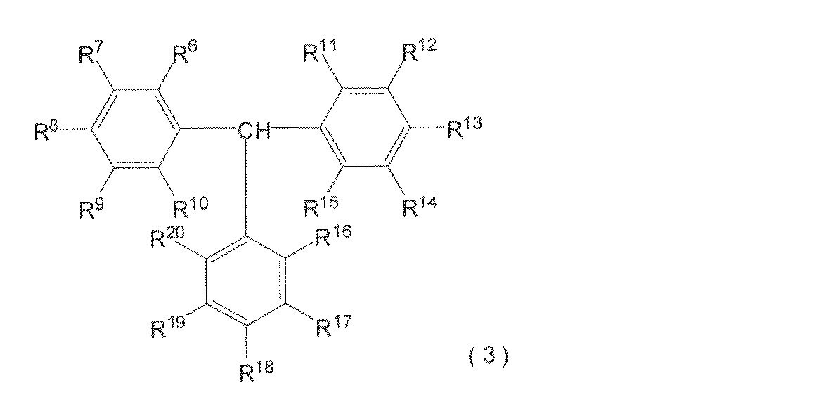
このような芳香族カルボン酸としては、例えば、安息香酸、フタル酸、イソフタル酸、テレフタル酸、ヘミメリット酸、トリメリット酸、トリメシン酸、メロファン酸、プレーニト酸、ピロメリット酸、メリット酸、キシリル酸、ヘメリト酸、メシチレン酸、プレーニチル酸、トルイル酸、ケイ皮酸、サリチル酸、2,3-ジヒドロキシ安息香酸、2,4-ジヒドロキシ安息香酸、ゲンチジン酸(2,5-ジヒドロキシ安息香酸)、2,6-ジヒドロキシ安息香酸、3,5-ジヒドロキシ安息香酸、没食子酸(3,4,5-トリヒドロキシ安息香酸)等の安息香酸誘導体、1,4-ジヒドロキシ-2-ナフトエ酸、3,5-ジヒドロキシ-2-ナフトエ酸、3,5-ジヒドロキシ-2-ナフトエ酸等のナフトエ酸誘導体、フェノールフタリン、ジフェノール酸等が挙げられ、これらのうち1種または2種以上を組み合わせて用いることができる。 [Wherein, R 6 to R 20 are each independently a monovalent organic group, and at least one of R 6 to R 20 is a hydroxyl group or a carboxyl group. ]
Examples of such aromatic carboxylic acids include benzoic acid, phthalic acid, isophthalic acid, terephthalic acid, hemimellitic acid, trimellitic acid, trimesic acid, merophanic acid, planitic acid, pyromellitic acid, meritic acid, and xylic acid. , Hemelitic acid, mesitylene acid, prenylic acid, toluic acid, cinnamic acid, salicylic acid, 2,3-dihydroxybenzoic acid, 2,4-dihydroxybenzoic acid, gentisic acid (2,5-dihydroxybenzoic acid), 2,6 -Benzoic acid derivatives such as dihydroxybenzoic acid, 3,5-dihydroxybenzoic acid, gallic acid (3,4,5-trihydroxybenzoic acid), 1,4-dihydroxy-2-naphthoic acid, 3,5-dihydroxy- 2-naphthoic acid, naphthoic acid derivatives such as 3,5-dihydroxy-2-naphthoic acid, phenolphthaline Diphenol acid and the like, it can be used singly or in combination of two or more of them.
フラックス機能を有する化合物以外の硬化剤としては、特に限定されないが、例えば、フェノール類、アミン類、チオール類等が挙げられる。このような硬化剤は、硬化性樹脂成分の種類等に応じて適宜選択することができる。例えば、硬化性樹脂成分としてエポキシ樹脂を使用する場合には、エポキシ樹脂との良好な反応性、硬化時の低寸法変化および硬化後の適切な物性(例えば、耐熱性、耐湿性等)が得られる点で硬化剤としてフェノール類を用いることが好ましく、硬化性樹脂成分の硬化後の物性が優れている点で2官能以上のフェノール類がより好ましく用いられる。なお、このような硬化剤は、1種単独で用いてもよいし、2種以上を併用して用いてもよい。 (Iv) Curing Agent The curing agent other than the compound having a flux function is not particularly limited, and examples thereof include phenols, amines, and thiols. Such a hardening | curing agent can be suitably selected according to the kind etc. of curable resin component. For example, when an epoxy resin is used as the curable resin component, good reactivity with the epoxy resin, low dimensional change during curing, and appropriate physical properties after curing (eg heat resistance, moisture resistance, etc.) are obtained. In view of the above, it is preferable to use a phenol as a curing agent, and a bifunctional or higher functional phenol is more preferably used in terms of excellent physical properties after curing of the curable resin component. In addition, such a hardening | curing agent may be used individually by 1 type, and may be used in combination of 2 or more type.
また、硬化性樹脂組成物には、上述した各種成分の他に、さらに、硬化促進剤を添加することができる。これにより、硬化性樹脂組成物を、確実かつ容易に硬化させることができる。 (V) Curing accelerator In addition to the various components described above, a curing accelerator can be further added to the curable resin composition. Thereby, a curable resin composition can be hardened reliably and easily.
また、硬化性樹脂組成物には、さらに、シランカップリング剤を添加することができる。 (Vi) Silane coupling agent A silane coupling agent can be further added to the curable resin composition.
(b)熱可塑性樹脂組成物
熱可塑性樹脂組成物は、熱可塑性樹脂成分およびフラックス機能を有する化合物を含有し、所定温度により軟化するものである。 Moreover, you may prepare the liquid curable resin composition by mixing each said component in a solvent or under absence of solvent. The solvent used at this time is not particularly limited as long as it is inert to each component. For example, acetone, methyl ethyl ketone (MEK), methyl isobutyl ketone (MIBK), diisobutyl ketone (DIBK), cyclohexanone, Ketones such as diacetone alcohol (DAA), aromatic hydrocarbons such as benzene, xylene and toluene, alcohols such as methyl alcohol, ethyl alcohol, isopropyl alcohol and n-butyl alcohol, methyl cellosolve, ethyl cellosolve, butyl cellosolve, Cellosolves such as methyl cellosolve acetate and ethyl cellosolve acetate, N-methyl-2-pyrrolidone (NMP), tetrahydrofuran (THF), dimethylformamide (DMF), dibasic acid ester (DBE), 3 Ethyl ethoxypropionate (EEP), dimethyl carbonate (DMC) and the like, can be used singly or in combination of two or more of them. The amount of solvent used is preferably such that the solid content concentration of the components mixed in the solvent is 10 to 60% by weight.
(B) Thermoplastic resin composition The thermoplastic resin composition contains a thermoplastic resin component and a compound having a flux function, and is softened at a predetermined temperature.
熱可塑性樹脂成分としては、特に限定されないが、例えば、酢酸ビニル系、ポリビニルアルコール樹脂、ポリビニルブチラール樹脂、塩化ビニル樹脂、(メタ)アクリル樹脂、フェノキシ樹脂、ポリエステル樹脂、ポリイミド樹脂、ポリアミドイミド樹脂、シロキサン変性ポリイミド樹脂、ポリブタジエン樹脂、アクリル樹脂、スチレン樹脂、ポリエチレン樹脂、ポリプロピレン樹脂、ポリアミド樹脂、セルロース樹脂、イソブチレン樹脂、ビニルエーテル樹脂、液晶ポリマー樹脂、ポリフェニレンスルフィド樹脂、ポリフェニレンエーテル樹脂、ポリエーテルサルフォン樹脂、ポリエーテルイミド樹脂、ポリエーテルエーテルケトン樹脂、ポリウレタン樹脂、スチレン-ブタジエン-スチレン共重合体、スチレン-エチレン-ブチレン-スチレン共重合体、ポリアセタール樹脂、ポリビニルアセタール樹脂、ブチルゴム、クロロプレンゴム、アクリロニトリル-ブタジエン共重合体、アクリロニトリル-ブタジエン-アクリル酸共重合体、アクリロニトリル-ブタジエン-スチレン共重合体、ポリ酢酸ビニル等が挙げられる。これら熱可塑性樹脂成分は、単一の重合体でもよく、これら熱可塑性樹脂成分の少なくとも2種以上の共重合体でもよい。 (I) Thermoplastic resin component The thermoplastic resin component is not particularly limited. For example, vinyl acetate, polyvinyl alcohol resin, polyvinyl butyral resin, vinyl chloride resin, (meth) acrylic resin, phenoxy resin, polyester resin, polyimide Resin, polyamideimide resin, siloxane-modified polyimide resin, polybutadiene resin, acrylic resin, styrene resin, polyethylene resin, polypropylene resin, polyamide resin, cellulose resin, isobutylene resin, vinyl ether resin, liquid crystal polymer resin, polyphenylene sulfide resin, polyphenylene ether resin, Polyethersulfone resin, polyetherimide resin, polyetheretherketone resin, polyurethane resin, styrene-butadiene-styrene copolymer, styrene- Tylene-butylene-styrene copolymer, polyacetal resin, polyvinyl acetal resin, butyl rubber, chloroprene rubber, acrylonitrile-butadiene copolymer, acrylonitrile-butadiene-acrylic acid copolymer, acrylonitrile-butadiene-styrene copolymer, polyvinyl acetate Etc. These thermoplastic resin components may be a single polymer, or may be a copolymer of at least two of these thermoplastic resin components.
フラックス機能を有する化合物としては、前述した「(a)硬化性樹脂組成物」において説明したものと同じものを用いることができる。さらに、好ましい化合物およびその配合量等についても同様である。 (Ii) Compound having a flux function As the compound having a flux function, the same compounds as those described in the above-mentioned "(a) curable resin composition" can be used. Further, the same applies to preferred compounds and their blending amounts.
また、熱可塑性樹脂成分およびフラックス機能を有する化合物の他、フィルム形成性樹脂、シランカップリング剤や、可塑剤、安定剤、粘着付与剤、滑剤、酸化防止剤、無機フィラー、充てん剤、帯電防止剤および顔料等が配合されていてもよいが、これらのものは、前述した「(a)硬化性樹脂組成物」において説明したものと同じものを用いることができる。さらに、好ましい化合物およびその配合量等についても同様である。 (Iii) Other additives In addition to thermoplastic resin components and compounds having a flux function, film-forming resins, silane coupling agents, plasticizers, stabilizers, tackifiers, lubricants, antioxidants, inorganics A filler, a filler, an antistatic agent, a pigment, and the like may be blended, and these can be the same as those described in the above-mentioned “(a) curable resin composition”. Further, the same applies to preferred compounds and their blending amounts.
<<金属層12>>
金属層(金属箔層)12は、低融点の金属材料で構成される金属箔で構成される層である。 Moreover, the conductive connection sheet 1 should just be provided with the at least 1 layer of resin composition layer, and even if any one of the 1st
<<
The metal layer (metal foil layer) 12 is a layer composed of a metal foil composed of a low melting point metal material.
<導電接続シートの製造方法>
上述した導電接続シート1は、例えば、以下のような製造方法により、製造することができる。 The thickness of the conductive connection sheet 1 is not particularly limited, but is preferably 1 μm or more, more preferably 3 μm or more, further preferably 5 μm or more, and preferably 200 μm or less. 150 μm or less is more preferable, and 100 μm or less is further preferable. When the thickness of the conductive connection sheet 1 is within the above range, the gap between the
<Method for producing conductive connection sheet>
The conductive connection sheet 1 described above can be manufactured, for example, by the following manufacturing method.
第1の樹脂組成物層11および第2の樹脂組成物層13を構成する樹脂組成物が、25℃で液状をなす場合、まず、金属層12を用意する。 (I) When the resin composition is in a liquid state at 25 ° C. When the resin composition constituting the first
第1の樹脂組成物層11および第2の樹脂組成物層13を構成する樹脂組成物が、25℃でフィルム状をなす場合、まず、ポリエステルシート等の剥離基材を用意する。 (Ii) When the resin composition forms a film at 25 ° C. When the resin composition constituting the first
<本発明の端子間の接続方法>
以下では、まず、本発明の端子間の接続方法を適用して、接続部81と封止層80とを形成する場合について詳述する。 The connection method between terminals of the present invention or the method of forming connection terminals of the present invention is applied to the formation of the
<Connection method between terminals of the present invention>
Below, the case where the
<<第1実施形態>>
導電接続シート1が備える樹脂組成物層11、13が硬化性樹脂組成物で構成される第1実施形態では、半導体チップ20と、配線パターン40が設けられたインターポーザー30との間に導電接続シート1を配置する配置工程と、金属層12の融点以上で、かつ、樹脂組成物層11、13を構成する硬化性樹脂組成物の硬化が完了しない温度で導電接続シート1を加熱する加熱工程と、硬化性樹脂組成物の硬化を完了させる硬化工程とを有している。 In addition, when forming the
<< First Embodiment >>
In the first embodiment in which the resin composition layers 11 and 13 provided in the conductive connection sheet 1 are formed of a curable resin composition, conductive connection is made between the
まず、半導体チップ20と、配線パターン40が設けられたインターポーザー30とを用意する。 [1] Arrangement Step First, the
次に、前記配置工程[1]において、半導体チップ20と、配線パターン40が設けられたインターポーザー30との間に配置された導電接続シート1を、図4(b)に示すように、金属層12の融点以上で加熱する。 [2] Heating Step Next, in the arrangement step [1], the conductive connection sheet 1 arranged between the
より具体的には、まず、銅板(例えば、縦1.0cm×横1.0cm×厚さ0.3mm)90を用意し、この銅板90上に、厚さ30μmの樹脂組成物層11を形成した後、さらに、この樹脂組成物層11上に、直径Dが0.5mmの金属ボール91を配置する(図5(a)参照。)。 S [%] = (DH) / D × 100 Formula 1
More specifically, first, a copper plate (for example, length 1.0 cm × width 1.0 cm × thickness 0.3 mm) 90 is prepared, and a
樹脂組成物層11の酸価量は、3.0×10⁻⁵~1.0×10⁻²mol/gであるのが好ましく、8×10-5~5×10-3mol/gであるのがより好ましい。これにより、金属ボール91の濡れ広がり率をより確実に37%以上に設定することができる。 Acid value [mol / g] = (A × C) / M Equation 2
The acid value of the
次に、前記加熱工程[2]において、接続部81と封止層80とを形成した後、硬化性樹脂組成物を硬化させることにより、封止層80を固定する。 [3] Curing Step Next, in the heating step [2], after forming the connecting
<<第2実施形態>>
導電接続シート1が備える樹脂組成物層11、13が熱可塑性樹脂組成物で構成される第2実施形態では、半導体チップ20と、配線パターン40が設けられたインターポーザー30との間に導電接続シート1を配置する配置工程と、金属層12の融点以上で、かつ、樹脂組成物層11、13を構成する熱可塑性樹脂組成物が軟化する温度で導電接続シート1を加熱する加熱工程と、熱可塑性樹脂組成物を固化させる固化工程とを有している。 Through the steps as described above, the
<< Second Embodiment >>
In the second embodiment in which the resin composition layers 11 and 13 included in the conductive connection sheet 1 are formed of a thermoplastic resin composition, conductive connection is made between the
樹脂組成物層11、13が熱可塑性樹脂組成物で構成される本実施形態においても、樹脂組成物層11、13が熱硬化性樹脂組成物で構成される前記第1実施形態と同様にして、端子21と端子41とがそれぞれ対向した状態で、半導体チップ20と、配線パターン40が設けられたインターポーザー30との間に、導電接続シート1を配置する。 [1] Arrangement Step The first embodiment in which the resin composition layers 11 and 13 are made of a thermosetting resin composition also in the present embodiment in which the resin composition layers 11 and 13 are made of a thermoplastic resin composition. Similarly to the embodiment, the conductive connection sheet 1 is disposed between the
次に、前記配置工程[1]において、半導体チップ20と、配線パターン40が設けられたインターポーザー30との間に配置された導電接続シート1を、図4(b)に示すように、金属層12の融点以上の温度で加熱する。 [2] Heating Step Next, in the arrangement step [1], the conductive connection sheet 1 arranged between the
次に、前記加熱工程[2]において、接続部81と封止層80とを形成した後、熱可塑性樹脂組成物を固化させることにより、封止層80を固定する。 [3] Solidification Step Next, in the heating step [2], after forming the
<本発明の接続端子の形成方法>
次に、本発明の接続端子の形成方法を用いて、接続部81と封止層80とを形成する場合について説明する。 In the first embodiment and the second embodiment, the case where the
<Method for Forming Connection Terminal of the Present Invention>
Next, the case where the
<<第3実施形態>>
導電接続シート1が備える樹脂組成物層11、13が硬化性樹脂組成物で構成される第3実施形態では、半導体チップ20の端子21側の面に、導電接続シート1を配置する配置工程と、金属層12の融点以上で、かつ、樹脂組成物層11、13を構成する硬化性樹脂組成物の硬化が完了しない温度で導電接続シート1を加熱する加熱工程とを有している。 In addition, when forming the
<< Third Embodiment >>
In the third embodiment in which the resin composition layers 11 and 13 provided in the conductive connection sheet 1 are formed of a curable resin composition, an arrangement step of arranging the conductive connection sheet 1 on the surface of the
まず、図6(a)に示すように、下面側に端子21を備える半導体チップ20を用意する。 [1] Arrangement Step First, as shown in FIG. 6A, a
次に、前記配置工程[1]において、半導体チップ20の端子21側の面に配置された導電接続シート1(金属層12)を、図6(b)に示すように、金属層12の融点以上で加熱する。 [2] Heating step Next, in the placement step [1], the conductive connection sheet 1 (metal layer 12) placed on the surface on the terminal 21 side of the
<<第4実施形態>>
導電接続シート1が備える樹脂組成物層11、13が熱可塑性樹脂組成物で構成される第4実施形態では、半導体チップ20の端子21側の面に、導電接続シート1を配置する配置工程と、金属層12の融点以上で、かつ、樹脂組成物層11、13を構成する熱可塑性樹脂組成物が軟化する温度で導電接続シート1を加熱する加熱工程とを有している。 And in this embodiment, since the curable resin component is contained as a resin component contained in the resin composition layers 11 and 13 and this thing exists in an uncured state, the curable resin composition is cured. By doing so, the
<< Fourth Embodiment >>
In the fourth embodiment in which the resin composition layers 11 and 13 included in the conductive connection sheet 1 are made of a thermoplastic resin composition, an arrangement step of arranging the conductive connection sheet 1 on the surface of the
樹脂組成物層11、13が熱可塑性樹脂組成物で構成される本実施形態においても、樹脂組成物層11、13が熱硬化性樹脂組成物で構成される前記第3実施形態と同様にして、半導体チップ20の端子21側に導電接続シート1を熱圧着(配置)させて、半導体チップ20の端子21側の面において露出する端子21に、導電接続シート1を接触させる。 [1] Arrangement Step The third embodiment in which the resin composition layers 11 and 13 are made of a thermosetting resin composition also in the present embodiment in which the resin composition layers 11 and 13 are made of a thermoplastic resin composition. In the same manner as in the embodiment, the conductive connection sheet 1 is thermocompression-bonded (arranged) on the terminal 21 side of the
次に、前記配置工程[1]において、半導体チップ20の端子21側の面に配置された導電接続シート1(金属層12)を、図6(b)に示すように、金属層12の融点以上で加熱する。 [2] Heating step Next, in the placement step [1], the conductive connection sheet 1 (metal layer 12) placed on the surface on the terminal 21 side of the
各実施例および各比較例の導電接続シートを用いて、対向する端子同士を接続するために作製した端子接続体において、端子間の接続抵抗、導通路(接続部)形成性および導通路以外の領域に位置する封止層に残存する金属層の有無を以下の方法により測定または評価した。 1. Evaluation method In the terminal connection body produced in order to connect opposing terminals using the conductive connection sheet of each Example and each comparative example, the connection resistance between terminals, a conduction path (connection part) formability, and a conduction path The presence or absence of a metal layer remaining in the sealing layer located in a region other than the above was measured or evaluated by the following method.
得られた端子接続体中の対向する端子間の抵抗を4端子法(抵抗計:岩崎通信機(株)製、「デジタルマルチメータVOA7510」、測定プローブ:日置電機(株)製「ピン型リード9771」)により12点測定し、その平均値が30mΩ未満の場合を「A」、30mΩ以上の場合を「B」と判定した。 (1) Connection resistance The resistance between opposing terminals in the obtained terminal connection body was determined by a four-terminal method (resistance meter: manufactured by Iwasaki Tsushinki Co., Ltd., “Digital Multimeter VOA7510”, measurement probe: Hioki Electric Co., Ltd.) 12 points were measured by “Pin type lead 9771” manufactured by the manufacturer, and when the average value was less than 30 mΩ, it was determined as “A”, and when it was 30 mΩ or more, it was determined as “B”.
得られた端子接続体中の対向する端子10組について、その端子間の断面を走査型電子顕微鏡(日本電子(株)製、「JSM-7401F」)で観察し、10組全てにおいて半田により円柱状の導通路(接続部)が形成されている場合を「A」、1組でも導通路が形成されていない端子が存在する場合を「B」、隣接している端子とショート接触している場合を「C」と判定した。 (2) Conducting path forming property With respect to 10 sets of opposing terminals in the obtained terminal connection body, the cross section between the terminals was observed with a scanning electron microscope (“JSM-7401F” manufactured by JEOL Ltd.), “A” indicates that a cylindrical conductive path (connecting portion) is formed by solder in all 10 sets, and “B” indicates that there is a terminal in which no conductive path is formed even in one set, which are adjacent. The case of short contact with the terminal was determined as “C”.
得られた端子接続体の断面を走査型電子顕微鏡(SEM)(日本電子社製、型番「JSM-7401F」)で観察し、全ての金属層(金属材料)が対向する端子間の導通路形成に寄与している場合を「A」、導通路形成に寄与せずに対向する端子間(接続部)以外の樹脂(封止層)中に金属層の一部が残存している場合を「B」と判定した。 (3) Presence or absence of residual solder The cross section of the obtained terminal connection body is observed with a scanning electron microscope (SEM) (manufactured by JEOL Ltd., model number “JSM-7401F”), and all metal layers (metal materials) face each other. "A" when contributing to the formation of the conduction path between the terminals to be performed, a part of the metal layer is in the resin (sealing layer) other than between the terminals (connection portion) facing each other without contributing to the formation of the conduction path The case where it remained was determined as “B”.
各実施例および各比較例の導電接続シートが備える樹脂組成物層中に、金属ボールを、その少なくとも一部が埋入するように配置した状態で、この金属ボールを加熱することにより溶融した際における金属ボールの濡れ広がり率を求めた。 2. Measurement of Wetting and Spreading Ratio of Metal Ball In a state where the metal ball is disposed so that at least a part of the metal ball is embedded in the resin composition layer provided in the conductive connection sheet of each example and each comparative example. The wetting and spreading rate of the metal balls when melted by heating was determined.
各実施例および各比較例の導電接続シートが備える樹脂組成物層の酸価量を、電位差滴定法を用いて測定した。 3. Measurement of Acid Value Amount of Resin Composition Layer The acid value amount of the resin composition layer included in the conductive connection sheet of each example and each comparative example was measured using a potentiometric titration method.
[実施例1~6、比較例1、2]
まず、エポキシ樹脂として、ビスフェノールA型エポキシ樹脂(大日本インキ化学工業社製、「EPICLON-840S」、エポキシ当量185g/eq)を、硬化剤として、フェノールノボラック樹脂(住友ベークライト社製、「PR-53647」)を、フィルム形成性樹脂として、変性ビフェノール型エポキシ樹脂(ジャパンエポキシレジン社製、「YX-6954」)を、フラックス機能を有する化合物として、セバシン酸(東京化成工業社製、化合物1)、ゲンチジン酸(みどり化学社製、化合物2)およびフェノールフタリン(東京化成工業社製、化合物3)を、シランカップリング剤として、2-(3,4-エポキシシクロヘキシル)エチルトリメトキシシラン(信越化学工業社製、「KBM-303」)を、硬化促進剤として、2-フェニル-4-メチルイミダゾール(四国化成工業社製、「キュアゾール2P4MZ」)をそれぞれ用意した。 4). Preparation of conductive connection sheet and sheet for measuring wetting spread rate [Examples 1 to 6, Comparative Examples 1 and 2]
First, bisphenol A type epoxy resin (manufactured by Dainippon Ink and Chemicals, "EPICLON-840S", epoxy equivalent 185 g / eq) is used as an epoxy resin, and phenol novolac resin (manufactured by Sumitomo Bakelite, "PR-" is used as a curing agent. 53647 ") as a film-forming resin, modified biphenol type epoxy resin (Japan Epoxy Resin Co., Ltd.," YX-6594 ") as a compound having a flux function, and sebacic acid (Tokyo Chemical Industry Co., Ltd., Compound 1) 2- (3,4-epoxycyclohexyl) ethyltrimethoxysilane (Shin-Etsu) using gentisic acid (manufactured by Midori Chemical Co., Compound 2) and phenolphthaline (manufactured by Tokyo Chemical Industry Co., Ltd., Compound 3) as silane coupling agents “KBM-303” manufactured by Chemical Industry Co., Ltd. Te, 2-phenyl-4-methylimidazole (Shikoku Chemicals Corporation, "Curezol 2P4MZ") were prepared, respectively.
次に、各実施例および各比較例の導電接続シートを用いて、対向する端子間の接続を行った。 5. Connection Between Terminals Using Conductive Connection Sheet Next, connection between opposing terminals was performed using the conductive connection sheets of each Example and each Comparative Example.
各実施例および各比較例用に調製した樹脂組成物を乾燥させたものを、それぞれ、0.2gずつ秤量し、その後、これらのものを前述した樹脂組成物層の酸価量の測定方法を用いて、その酸化量を求めた。その結果を表1、2に示す。 6). Measurement of acid value of resin composition layer provided in conductive connection sheet 0.2 g of each dried resin composition prepared for each example and each comparative example was weighed, and then those The amount of oxidation was determined using the method for measuring the acid value of the resin composition layer described above. The results are shown in Tables 1 and 2.


Claims (19)
- 樹脂成分と、フラックス機能を有する化合物とを含有する樹脂組成物で構成される樹脂組成物層と、低融点の金属材料で構成される金属層とを備える積層体により構成される導電接続シートであって、
前記樹脂組成物層は、下記要件Aを満足することを特徴とする導電接続シート。
要件A: 前記樹脂組成物層中に低融点の金属材料で構成される金属ボールの少なくとも一部を配置した状態で、JIS Z 3197に規定の半田付用樹脂系フラックス試験方法に準拠して、前記金属ボールの溶融温度以上に加熱し、その後、前記金属ボールの濡れ広がり率を測定したとき、該濡れ広がり率が37%以上となる。 A conductive connection sheet comprising a laminate comprising a resin composition comprising a resin component and a resin composition containing a compound having a flux function, and a metal layer comprising a metal material having a low melting point. There,
The said resin composition layer satisfies the following requirement A, The electrically conductive connection sheet | seat characterized by the above-mentioned.
Requirement A: In a state where at least a part of a metal ball composed of a low melting point metal material is disposed in the resin composition layer, in accordance with the soldering resin flux test method specified in JIS Z 3197, When the metal ball is heated to a melting temperature or higher and then the wet spread rate of the metal ball is measured, the wet spread rate is 37% or higher. - 前記濡れ広がり率S[%]は、加熱前の前記金属ボールの直径をD[mm]とし、加熱後の前記金属ボールの高さをH[mm]としたとき、下記式1により求められる請求項1に記載の導電接続シート。
S[%]=(D-H)/D×100 ・・・ 式1 The wet spreading rate S [%] is obtained by the following formula 1 when the diameter of the metal ball before heating is D [mm] and the height of the metal ball after heating is H [mm]. Item 2. The conductive connection sheet according to Item 1.
S [%] = (DH) / D × 100 Formula 1 - 前記金属ボールは、錫(Sn)、鉛(Pb)、銀(Ag)、ビスマス(Bi)、インジウム(In)、亜鉛(Zn)、ニッケル(Ni)、アンチモン(Sb)、鉄(Fe)、アルミニウム(Al)、金(Au)、ゲルマニウム(Ge)および銅(Cu)からなる群から選択される少なくとも2種以上の金属の合金または錫の単体である請求項1または2に記載の導電接続シート。 The metal balls are tin (Sn), lead (Pb), silver (Ag), bismuth (Bi), indium (In), zinc (Zn), nickel (Ni), antimony (Sb), iron (Fe), 3. The conductive connection according to claim 1, wherein the conductive connection is an alloy of at least two kinds of metals selected from the group consisting of aluminum (Al), gold (Au), germanium (Ge), and copper (Cu), or a simple substance of tin. Sheet.
- 前記金属ボールは、Sn-Pb合金、Sn-Ag-Cu合金またはSn-Ag合金を主材料として構成される請求項3に記載の導電接続シート。 4. The conductive connection sheet according to claim 3, wherein the metal ball is composed mainly of a Sn—Pb alloy, a Sn—Ag—Cu alloy, or a Sn—Ag alloy.
- 前記金属ボールは、Sn-37Pb合金またはSn-3.0Ag-0.5Cu合金を主材料として構成される請求項4に記載の導電接続シート。 5. The conductive connection sheet according to claim 4, wherein the metal ball is composed of a Sn-37Pb alloy or a Sn-3.0Ag-0.5Cu alloy as a main material.
- 前記金属ボールは、加熱前の直径が0.5mmである請求項1ないし5のいずれかに記載の導電接続シート。 The conductive connection sheet according to any one of claims 1 to 5, wherein the metal ball has a diameter of 0.5 mm before heating.
- 前記樹脂組成物は、その酸価量が3.0×10⁻⁵~1.0×10⁻²mol/gである請求項1ないし6のいずれかに記載の導電接続シート。 7. The conductive connection sheet according to claim 1, wherein the resin composition has an acid value of 3.0 × 10 −5 to 1.0 × 10 −2 mol / g.
- 前記酸価量は、酸化還元滴定法を用いて算出される請求項1ないし7のいずれかに記載の導電接続シート。 The conductive connection sheet according to any one of claims 1 to 7, wherein the acid value is calculated using a redox titration method.
- 前記樹脂組成物において、前記フラックス機能を有する化合物の含有量は、1~50重量%である請求項1ないし8のいずれかに記載の導電接続シート。 9. The conductive connection sheet according to claim 1, wherein the content of the compound having a flux function in the resin composition is 1 to 50% by weight.
- 前記フラックス機能を有する化合物は、フェノール性水酸基およびカルボキシル基のうちの少なくとも一方を有する化合物を含有する請求項1ないし9のいずれかに記載の導電接続シート。 The conductive connection sheet according to any one of claims 1 to 9, wherein the compound having a flux function contains a compound having at least one of a phenolic hydroxyl group and a carboxyl group.
- 前記フラックス機能を有する化合物は、下記一般式(1)で表わされる化合物を含有する請求項10に記載の導電接続シート。
HOOC-(CH2)n-COOH・・・・・(1)
(式(1)中、nは、1~20の整数である。) The conductive connection sheet according to claim 10, wherein the compound having a flux function contains a compound represented by the following general formula (1).
HOOC- (CH 2 ) n-COOH (1)
(In formula (1), n is an integer of 1 to 20) - 前記フラックス機能を有する化合物は、下記一般式(2)および下記一般式(3)で表わされる化合物のうちの少なくとも一方を含有する請求項10に記載の導電接続シート。

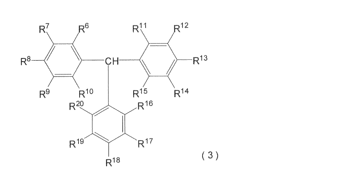
- 前記積層体は、2つの前記樹脂組成物層および1つの前記金属層で構成され、前記樹脂組成物層、金属層および前記樹脂組成物層がこの順で積層されたものである請求項1ないし12のいずれかに記載の導電接続シート。 The laminate is composed of two resin composition layers and one metal layer, and the resin composition layer, metal layer, and resin composition layer are laminated in this order. The conductive connection sheet according to any one of 12.
- 請求項1ないし13のいずれかに記載の導電接続シートを対向する端子間に配置する配置工程と、前記金属材料の融点以上であり、かつ、前記樹脂組成物の硬化が完了しない温度で前記導電接続シートを加熱する加熱工程と、前記樹脂組成物を硬化させる硬化工程とを有することを特徴とする端子間の接続方法。 The arrangement | positioning process which arrange | positions the electrically-conductive connection sheet in any one of Claims 1 thru | or 13 between the terminals which oppose, and it is more than melting | fusing point of the said metal material, and the said electroconductivity is the temperature at which hardening of the said resin composition is not completed. A method for connecting terminals, comprising: a heating step for heating the connection sheet; and a curing step for curing the resin composition.
- 請求項1ないし13のいずれかに記載の導電接続シートを対向する端子間に配置する配置工程と、前記金属材料の融点以上であり、かつ、前記樹脂組成物が軟化する温度で前記導電接続シートを加熱する加熱工程と、前記樹脂組成物を固化させる固化工程とを有することを特徴とする端子間の接続方法。 The arrangement | positioning process which arrange | positions between the terminals which oppose the electrically conductive connection sheet in any one of Claim 1 thru | or 13, The said electrically conductive connection sheet at the temperature which is more than melting | fusing point of the said metal material, and the said resin composition softens A method for connecting terminals, comprising: a heating step for heating the resin composition; and a solidification step for solidifying the resin composition.
- 請求項1ないし13のいずれかに記載の導電接続シートを電子部材の電極上に配置する配置工程と、前記金属材料の融点以上であり、かつ、前記樹脂組成物の硬化が完了しない温度で前記導電接続シートを加熱する加熱工程とを有することを特徴とする接続端子の形成方法。 The disposing step of disposing the conductive connection sheet according to any one of claims 1 to 13 on an electrode of an electronic member, the melting point of the metal material, and a temperature at which the curing of the resin composition is not completed And a heating step of heating the conductive connection sheet.
- 請求項1ないし13のいずれかに記載の導電接続シートを電子部材の電極上に配置する配置工程と、前記金属箔の融点以上であり、かつ、前記樹脂組成物が軟化する温度で前記導電接続シートを加熱する加熱工程とを有することを特徴とする接続端子の形成方法。 The arrangement | positioning process which arrange | positions the electroconductive connection sheet in any one of Claim 1 thru | or 13 on the electrode of an electronic member, It is more than melting | fusing point of the said metal foil, and the said electroconductive connection is the temperature which the said resin composition softens And a heating step of heating the sheet.
- 対向する端子同士が、請求項1ないし13のいずれかに記載の導電接続シートを用いて形成された接続部を介して電気的に接続されていることを特徴とする半導体装置。 14. A semiconductor device, wherein terminals facing each other are electrically connected via a connection portion formed using the conductive connection sheet according to any one of claims 1 to 13.
- 対向する端子同士が、請求項1ないし13のいずれかに記載の導電接続シートを用いて形成された接続部を介して電気的に接続されていることを特徴とする電子機器。 An electronic device, wherein terminals facing each other are electrically connected through a connection portion formed using the conductive connection sheet according to any one of claims 1 to 13.
Priority Applications (6)
| Application Number | Priority Date | Filing Date | Title |
|---|---|---|---|
| CN201180007138.9A CN102725912B (en) | 2010-01-29 | 2011-01-18 | The formation method of the method for attachment between conductive connecting piece, terminal, splicing ear, semiconductor device and electronic equipment |
| KR1020127022345A KR101622438B1 (en) | 2010-01-29 | 2011-01-18 | Conductive connection sheet, method for connecting terminals, method for forming connection terminal, semiconductor device, and electronic device |
| US13/575,718 US20120319268A1 (en) | 2010-01-29 | 2011-01-18 | Conductive connection sheet, method for connecting terminals, method for forming connection terminal, semiconductor device, and electronic device |
| EP11736877.9A EP2530786A4 (en) | 2010-01-29 | 2011-01-18 | Conductive connection sheet, method for connecting terminals, method for forming connection terminal, semiconductor device, and electronic device |
| JP2011551804A JP5664558B2 (en) | 2010-01-29 | 2011-01-18 | Conductive connection sheet, connection method between terminals, formation method of connection terminal, semiconductor device and electronic device |
| SG2012056198A SG182787A1 (en) | 2010-01-29 | 2011-01-18 | Conductive connection sheet, method for connecting terminals, method for forming connection terminal, semiconductor device, and electronic device |
Applications Claiming Priority (2)
| Application Number | Priority Date | Filing Date | Title |
|---|---|---|---|
| JP2010019737 | 2010-01-29 | ||
| JP2010-019737 | 2010-01-29 |
Publications (1)
| Publication Number | Publication Date |
|---|---|
| WO2011093162A1 true WO2011093162A1 (en) | 2011-08-04 |
Family
ID=44319154
Family Applications (1)
| Application Number | Title | Priority Date | Filing Date |
|---|---|---|---|
| PCT/JP2011/050684 WO2011093162A1 (en) | 2010-01-29 | 2011-01-18 | Conductive connection sheet, method for connecting terminals, method for forming connection terminal, semiconductor device, and electronic device |
Country Status (8)
| Country | Link |
|---|---|
| US (1) | US20120319268A1 (en) |
| EP (1) | EP2530786A4 (en) |
| JP (1) | JP5664558B2 (en) |
| KR (1) | KR101622438B1 (en) |
| CN (1) | CN102725912B (en) |
| SG (1) | SG182787A1 (en) |
| TW (1) | TWI533382B (en) |
| WO (1) | WO2011093162A1 (en) |
Cited By (3)
| Publication number | Priority date | Publication date | Assignee | Title |
|---|---|---|---|---|
| JP2015119163A (en) * | 2013-12-18 | 2015-06-25 | コリア アトミック エナジー リサーチ インスティテュートKoreaAtomic Energy Research Institute | Mounting substrate for surface-mounting semiconductor sensor and mounting method of the same |
| JP2018063950A (en) * | 2012-05-14 | 2018-04-19 | 積水化学工業株式会社 | Conductive particle material, conductive material, connection structure, and method for producing connection structure |
| KR20190053655A (en) * | 2017-11-10 | 2019-05-20 | 조인셋 주식회사 | Electric connecting terminal for metal case |
Families Citing this family (12)
| Publication number | Priority date | Publication date | Assignee | Title |
|---|---|---|---|---|
| CN103846549B (en) * | 2012-11-29 | 2016-02-10 | 北京航星机器制造公司 | A kind of laser welding packaging method of electronics member and electronic product casing |
| US9196559B2 (en) * | 2013-03-08 | 2015-11-24 | Taiwan Semiconductor Manufacturing Company, Ltd. | Directly sawing wafers covered with liquid molding compound |
| JP6049606B2 (en) * | 2013-12-25 | 2016-12-21 | 株式会社ノリタケカンパニーリミテド | Heat-curing conductive paste |
| US9899330B2 (en) * | 2014-10-03 | 2018-02-20 | Mc10, Inc. | Flexible electronic circuits with embedded integrated circuit die |
| TW201731603A (en) * | 2016-03-02 | 2017-09-16 | Dijiya Energy Saving Tech Inc | Lithium battery conductive connection piece and forming method thereof enabling to meet the use needs of charging and discharging of large current having high amplification factor |
| GB201613051D0 (en) | 2016-07-28 | 2016-09-14 | Landa Labs (2012) Ltd | Applying an electrical conductor to a substrate |
| JP2018035286A (en) * | 2016-09-01 | 2018-03-08 | パナソニックIpマネジメント株式会社 | Conductive resin composition and electronic circuit member using the same |
| JP6495368B2 (en) * | 2017-04-19 | 2019-04-03 | 立山科学工業株式会社 | Electronic module |
| KR101977473B1 (en) * | 2017-07-27 | 2019-05-10 | 주식회사 기가레인 | Flux diffusion is improved probe pin and method of manufacturing the same |
| EP3547352B1 (en) * | 2018-03-27 | 2020-09-30 | Infineon Technologies AG | Method for joining two joining members |
| US10971471B2 (en) * | 2018-12-29 | 2021-04-06 | Micron Technology, Inc. | Methods and systems for manufacturing semiconductor devices |
| JP7135880B2 (en) * | 2019-01-18 | 2022-09-13 | 株式会社オートネットワーク技術研究所 | Connecting terminal |
Citations (5)
| Publication number | Priority date | Publication date | Assignee | Title |
|---|---|---|---|---|
| JPS61276873A (en) | 1985-05-31 | 1986-12-06 | Sony Chem Kk | Electrically conductive anisotropic adhesive |
| JP2004114104A (en) * | 2002-09-26 | 2004-04-15 | Omae Seiko Kk | Flux for soldering |
| JP2004244486A (en) * | 2003-02-13 | 2004-09-02 | Sumitomo Bakelite Co Ltd | Adhesive film, and semiconductor package and semiconductor device using it |
| JP2004260131A (en) | 2003-02-05 | 2004-09-16 | Japan Science & Technology Agency | Connection method between terminals, and packaging method of semiconductor device |
| JP2009262227A (en) * | 2008-04-02 | 2009-11-12 | Hitachi Chem Co Ltd | Flux activator, adhesive resin composition, adhesive paste, adhesive film, semiconductor device fabrication method, and semiconductor device |
Family Cites Families (9)
| Publication number | Priority date | Publication date | Assignee | Title |
|---|---|---|---|---|
| JP2004209852A (en) * | 2003-01-06 | 2004-07-29 | Sumitomo Bakelite Co Ltd | Bump built-in double-side copper-clad sheet |
| KR101057608B1 (en) * | 2003-02-05 | 2011-08-18 | 고조 후지모토 | How to connect between terminals and mounting method of semiconductor device |
| JP2005203693A (en) * | 2004-01-19 | 2005-07-28 | Mitsubishi Electric Corp | Method for mounting connection sheet and surface-mounted component |
| TW200633810A (en) * | 2004-12-28 | 2006-10-01 | Arakawa Chem Ind | Lead-free solder flux and solder paste |
| US7732920B2 (en) * | 2005-03-28 | 2010-06-08 | Panasonic Corporation | Flip chip mounting body, flip chip mounting method and flip chip mounting apparatus |
| JP5217260B2 (en) | 2007-04-27 | 2013-06-19 | 住友ベークライト株式会社 | Semiconductor wafer bonding method and semiconductor device manufacturing method |
| US8039305B2 (en) * | 2007-04-27 | 2011-10-18 | Sumitomo Bakelite Company, Ltd. | Method for bonding semiconductor wafers and method for manufacturing semiconductor device |
| US20110311790A1 (en) * | 2008-09-05 | 2011-12-22 | Sumitomo Bakelite Co., Ltd. | Conductive connecting material, method for connecting terminals using the conductive connecting material, and method for producing a connecting terminal |
| JP4924773B2 (en) * | 2009-12-24 | 2012-04-25 | 住友ベークライト株式会社 | Conductive connection material, method for manufacturing electronic component, electronic member with conductive connection material, and electronic component |
-
2011
- 2011-01-18 KR KR1020127022345A patent/KR101622438B1/en not_active IP Right Cessation
- 2011-01-18 SG SG2012056198A patent/SG182787A1/en unknown
- 2011-01-18 EP EP11736877.9A patent/EP2530786A4/en not_active Withdrawn
- 2011-01-18 US US13/575,718 patent/US20120319268A1/en not_active Abandoned
- 2011-01-18 CN CN201180007138.9A patent/CN102725912B/en not_active Expired - Fee Related
- 2011-01-18 WO PCT/JP2011/050684 patent/WO2011093162A1/en active Application Filing
- 2011-01-18 JP JP2011551804A patent/JP5664558B2/en not_active Expired - Fee Related
- 2011-01-21 TW TW100102339A patent/TWI533382B/en not_active IP Right Cessation
Patent Citations (5)
| Publication number | Priority date | Publication date | Assignee | Title |
|---|---|---|---|---|
| JPS61276873A (en) | 1985-05-31 | 1986-12-06 | Sony Chem Kk | Electrically conductive anisotropic adhesive |
| JP2004114104A (en) * | 2002-09-26 | 2004-04-15 | Omae Seiko Kk | Flux for soldering |
| JP2004260131A (en) | 2003-02-05 | 2004-09-16 | Japan Science & Technology Agency | Connection method between terminals, and packaging method of semiconductor device |
| JP2004244486A (en) * | 2003-02-13 | 2004-09-02 | Sumitomo Bakelite Co Ltd | Adhesive film, and semiconductor package and semiconductor device using it |
| JP2009262227A (en) * | 2008-04-02 | 2009-11-12 | Hitachi Chem Co Ltd | Flux activator, adhesive resin composition, adhesive paste, adhesive film, semiconductor device fabrication method, and semiconductor device |
Non-Patent Citations (1)
| Title |
|---|
| See also references of EP2530786A4 |
Cited By (4)
| Publication number | Priority date | Publication date | Assignee | Title |
|---|---|---|---|---|
| JP2018063950A (en) * | 2012-05-14 | 2018-04-19 | 積水化学工業株式会社 | Conductive particle material, conductive material, connection structure, and method for producing connection structure |
| JP2015119163A (en) * | 2013-12-18 | 2015-06-25 | コリア アトミック エナジー リサーチ インスティテュートKoreaAtomic Energy Research Institute | Mounting substrate for surface-mounting semiconductor sensor and mounting method of the same |
| KR20190053655A (en) * | 2017-11-10 | 2019-05-20 | 조인셋 주식회사 | Electric connecting terminal for metal case |
| KR102026465B1 (en) | 2017-11-10 | 2019-09-27 | 조인셋 주식회사 | Electric connecting terminal for metal case |
Also Published As
| Publication number | Publication date |
|---|---|
| JPWO2011093162A1 (en) | 2013-05-30 |
| TWI533382B (en) | 2016-05-11 |
| TW201142964A (en) | 2011-12-01 |
| JP5664558B2 (en) | 2015-02-04 |
| KR20130033343A (en) | 2013-04-03 |
| KR101622438B1 (en) | 2016-05-18 |
| SG182787A1 (en) | 2012-08-30 |
| US20120319268A1 (en) | 2012-12-20 |
| EP2530786A4 (en) | 2013-07-10 |
| EP2530786A1 (en) | 2012-12-05 |
| CN102725912A (en) | 2012-10-10 |
| CN102725912B (en) | 2016-04-06 |
Similar Documents
| Publication | Publication Date | Title |
|---|---|---|
| JP5664558B2 (en) | Conductive connection sheet, connection method between terminals, formation method of connection terminal, semiconductor device and electronic device | |
| JP4924773B2 (en) | Conductive connection material, method for manufacturing electronic component, electronic member with conductive connection material, and electronic component | |
| JP4730484B2 (en) | Conductive connection material, connection method between terminals, and manufacturing method of connection terminals | |
| JP4752985B2 (en) | Conductive connection material and connection method between terminals using the same | |
| JP2011171258A (en) | Conductive connection sheet, method of connecting between terminals, method of forming connection terminal, semiconductor device, and electronic apparatus | |
| JP5482143B2 (en) | Conductive connection material, connection method between terminals, and manufacturing method of connection terminals | |
| JP2014075317A (en) | Conductive connection sheet, semiconductor device and electronic apparatus | |
| JP5564964B2 (en) | Conductive connection sheet, connection method between terminals, formation method of connection terminal, semiconductor device and electronic device | |
| JP5471551B2 (en) | Conductive connection sheet, connection method between terminals, formation method of connection terminal, semiconductor device and electronic device | |
| JP2011181467A (en) | Method for manufacturing conductive connection sheet, connection method between terminals, method for forming connection terminal, semiconductor device, and electronic device | |
| JP5447008B2 (en) | Connection method between terminals and method for manufacturing connection terminals | |
| JP5381775B2 (en) | Conductive connection sheet, connection method between terminals, formation method of connection terminal, semiconductor device and electronic device | |
| JP5381774B2 (en) | Method for forming solder layer, method for connecting terminals, semiconductor device and electronic device | |
| JP2011187487A (en) | Conductive connection sheet, method of making connection between terminals, method of forming connection terminal, and electronic apparatus | |
| JP2011165954A (en) | Conductive connection material, connection method between terminals, method of manufacturing connection terminal, electronic member, and electric and electronic component | |
| JP5544915B2 (en) | Conductive connection sheet, connection method between terminals, formation method of connection terminal, semiconductor device and electronic device | |
| JP5381784B2 (en) | Conductive connection sheet, connection method between terminals, formation method of connection terminal, semiconductor device and electronic device | |
| JP5381783B2 (en) | Conductive connection sheet, connection method between terminals, formation method of connection terminal, semiconductor device and electronic device | |
| JP5471601B2 (en) | Conductive connection sheet, connection method between terminals, formation method of connection terminal, semiconductor device and electronic device | |
| JP5381769B2 (en) | Connection method between terminals | |
| JP2014056992A (en) | Electronic device and electronic device manufacturing method | |
| JP2014082465A (en) | Conductive connection sheet, connection method between terminals, formation method of connection terminal, semiconductor device and electronic apparatus | |
| JP2011176143A (en) | Conductive connection sheet, method of connecting between terminals, method of forming connection terminal, semiconductor device, and electronic device | |
| JP2011181703A (en) | Method of manufacturing conductive connection sheet, method of connecting terminals, method of forming connection terminal, semiconductor device, and electronic equipment | |
| JP2012079527A (en) | Conductive connection sheet, method of connecting terminals, method of forming connection terminals, and electronic apparatus |
Legal Events
| Date | Code | Title | Description |
|---|---|---|---|
| WWE | Wipo information: entry into national phase |
Ref document number: 201180007138.9 Country of ref document: CN |
|
| 121 | Ep: the epo has been informed by wipo that ep was designated in this application |
Ref document number: 11736877 Country of ref document: EP Kind code of ref document: A1 |
|
| WWE | Wipo information: entry into national phase |
Ref document number: 2011551804 Country of ref document: JP |
|
| WWE | Wipo information: entry into national phase |
Ref document number: 12012501533 Country of ref document: PH |
|
| WWE | Wipo information: entry into national phase |
Ref document number: 13575718 Country of ref document: US Ref document number: 2011736877 Country of ref document: EP |
|
| NENP | Non-entry into the national phase |
Ref country code: DE |
|
| ENP | Entry into the national phase |
Ref document number: 20127022345 Country of ref document: KR Kind code of ref document: A |