WO2011065396A1 - 導電性ペースト及びプリント配線板、並びにその製造方法 - Google Patents
導電性ペースト及びプリント配線板、並びにその製造方法 Download PDFInfo
- Publication number
- WO2011065396A1 WO2011065396A1 PCT/JP2010/070974 JP2010070974W WO2011065396A1 WO 2011065396 A1 WO2011065396 A1 WO 2011065396A1 JP 2010070974 W JP2010070974 W JP 2010070974W WO 2011065396 A1 WO2011065396 A1 WO 2011065396A1
- Authority
- WO
- WIPO (PCT)
- Prior art keywords
- conductive paste
- vegetable oil
- binder resin
- wax
- epoxidized
- Prior art date
- Legal status (The legal status is an assumption and is not a legal conclusion. Google has not performed a legal analysis and makes no representation as to the accuracy of the status listed.)
- Ceased
Links
Images
Classifications
-
- H—ELECTRICITY
- H01—ELECTRIC ELEMENTS
- H01B—CABLES; CONDUCTORS; INSULATORS; SELECTION OF MATERIALS FOR THEIR CONDUCTIVE, INSULATING OR DIELECTRIC PROPERTIES
- H01B1/00—Conductors or conductive bodies characterised by the conductive materials; Selection of materials as conductors
- H01B1/20—Conductive material dispersed in non-conductive organic material
- H01B1/22—Conductive material dispersed in non-conductive organic material the conductive material comprising metals or alloys
-
- H—ELECTRICITY
- H05—ELECTRIC TECHNIQUES NOT OTHERWISE PROVIDED FOR
- H05K—PRINTED CIRCUITS; CASINGS OR CONSTRUCTIONAL DETAILS OF ELECTRIC APPARATUS; MANUFACTURE OF ASSEMBLAGES OF ELECTRICAL COMPONENTS
- H05K1/00—Printed circuits
- H05K1/02—Details
- H05K1/09—Use of materials for the conductive, e.g. metallic pattern
- H05K1/092—Dispersed materials, e.g. conductive pastes or inks
- H05K1/095—Dispersed materials, e.g. conductive pastes or inks for polymer thick films, i.e. having a permanent organic polymeric binder
-
- H—ELECTRICITY
- H05—ELECTRIC TECHNIQUES NOT OTHERWISE PROVIDED FOR
- H05K—PRINTED CIRCUITS; CASINGS OR CONSTRUCTIONAL DETAILS OF ELECTRIC APPARATUS; MANUFACTURE OF ASSEMBLAGES OF ELECTRICAL COMPONENTS
- H05K3/00—Apparatus or processes for manufacturing printed circuits
- H05K3/40—Forming printed elements for providing electric connections to or between printed circuits
- H05K3/4038—Through-connections; Vertical interconnect access [VIA] connections
- H05K3/4053—Through-connections; Vertical interconnect access [VIA] connections by thick-film techniques
- H05K3/4069—Through-connections; Vertical interconnect access [VIA] connections by thick-film techniques for via connections in organic insulating substrates
-
- H—ELECTRICITY
- H05—ELECTRIC TECHNIQUES NOT OTHERWISE PROVIDED FOR
- H05K—PRINTED CIRCUITS; CASINGS OR CONSTRUCTIONAL DETAILS OF ELECTRIC APPARATUS; MANUFACTURE OF ASSEMBLAGES OF ELECTRICAL COMPONENTS
- H05K2203/00—Indexing scheme relating to apparatus or processes for manufacturing printed circuits covered by H05K3/00
- H05K2203/12—Using specific substances
- H05K2203/122—Organic non-polymeric compounds, e.g. oil, wax or thiol
Definitions
- the present invention relates to a conductive paste containing a conductive metal material, a printed wiring board using the same, and a method for manufacturing the same.
- a substrate material in a B-stage state (semi-cured state) called a prepreg has been provided.
- Many of the B-stage substrate materials have relatively low heat resistance, and if the hot pressing is performed at a temperature necessary for interlayer connection, the substrate material characteristics may be deteriorated. For this reason, development of the electrically conductive paste which can perform interlayer connection at low temperature is desired.
- the conductive paste does not sufficiently diffuse into the conductor layer even though low melting point metal powder is used for the conductive paste, and the connection reliability between the layers decreases. End up.
- conductive paste sealed in an insulating material in a B-stage state does not sufficiently promote metal diffusion even when it is hot-pressed at a temperature high enough to deteriorate the material characteristics, and the interlayer connection Reliability will be reduced.
- the present invention has been proposed in view of the above circumstances, and an object thereof is to provide a conductive paste that improves the connection reliability between layers, a printed wiring board using the same, and a method of manufacturing the same.
- the present inventors have made it easier for metal diffusion of the conductive paste to proceed when any of epoxidized vegetable oil, esterified vegetable oil, and wax is contained as the binder resin of the conductive paste. And found that the connection reliability is improved.
- the conductive paste according to the present invention contains a binder resin and a conductive metal material in a conductive paste filled in a through via or a bottomed via provided in an insulating resin layer in a B stage state, and includes a binder.
- the resin is characterized by containing any one of epoxidized vegetable oil, esterified vegetable oil, and wax.
- the printed wiring board according to the present invention is a conductive printed circuit board in which a conductive paste is filled in a through via or a bottomed via provided in an insulating resin layer in a B-stage state, and the interlayer connection is performed by heat and pressure.
- the conductive paste contains a binder resin and a conductive metal material, and the binder resin contains any one of epoxidized vegetable oil, esterified vegetable oil, and wax.
- the printed wiring board manufacturing method includes a printed wiring board in which a conductive paste is filled in a through via or a bottomed via provided in an insulating resin layer in a B stage state, and the interlayer connection is performed by heating and pressing.
- the conductive paste contains a binder resin and a conductive metal material, and the binder resin contains any one of epoxidized vegetable oil, esterified vegetable oil, and wax.
- the conductive metal material of the conductive paste is easily diffused, and the connection reliability between the layers can be improved.
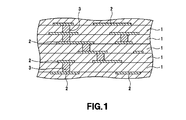
- FIG. 1 is a schematic cross-sectional view showing a configuration example of a multilayer wiring board.
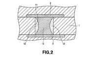
- FIG. 2 is a schematic cross-sectional view schematically showing a via-hole conductor.
- the conductive paste in the present embodiment contains a binder resin and a conductive metal material, and is a through via or bottomed via (hereinafter referred to as a prepreg) provided in an insulating resin layer in a B stage state (semi-cured state). Called via hole).
- a prepreg through via or bottomed via
- epoxidized vegetable oil, esterified vegetable oil, or wax is used as the binder resin.
- the binder resin epoxidized vegetable oil, esterified vegetable oil, or wax.
- Epoxidized vegetable oil is a compound obtained by epoxidizing an unsaturated double bond of vegetable oil using, for example, peracid.
- epoxidized vegetable oils include epoxidized soybean oil, epoxidized linseed oil, epoxidized castor oil, epoxidized corn oil, epoxidized rapeseed oil, epoxidized safflower oil, epoxidized sunflower oil, epoxidized palm oil, and epoxidized Examples include cottonseed oil, epoxidized olive oil, and epoxidized cocoa butter.
- low viscosity epoxidized soybean oil is preferably used.
- Esterified vegetable oil is a compound in which unsaturated fatty acid of vegetable oil and alcohol are ester-bonded.
- esterified vegetable oils include esterified soybean oil, esterified linseed oil, castor oil, esterified corn oil, esterified rapeseed oil, esterified safflower oil, esterified sunflower oil, esterified palm oil, esterified cottonseed oil, Examples include esterified olive oil and esterified cocoa butter.
- the vegetable oil which is a raw material for the epoxidized vegetable oil and esterified vegetable oil preferably contains at least one of oleic acid, linoleic acid and ⁇ -linolenic acid.
- specific examples of vegetable oils include soybean oil (about 20% oleic acid, about 50% linoleic acid, about 10% palmitic acid), linseed oil (about 40% ⁇ -linolenic acid), castor oil (about 87% ricinoleic acid, Oleic acid about 7%, linoleic acid about 3%), corn oil (linoleic acid about 55%, oleic acid about 30%, palmitic acid about 10%), rapeseed oil (oleic acid about 50%, linoleic acid 25-30%, ⁇ -linolenic acid 6-9%), safflower oil (conventional species: linoleic acid 73-82%, oleic acid 9-17%, high oleic: linoleic
- Wax is a compound in which a higher fatty acid and a higher alcohol are ester-bonded.
- specific examples of waxes include plant waxes such as carnauba wax and candelilla wax, animal waxes such as lanolin (wool wax) and lard, and synthetic waxes such as synthetic wood wax (hydrogenated vegetable oil and fat, oxidized wax). It is done.
- the conductive metal material of the conductive paste in this embodiment includes a low melting point metal and a high melting point metal, and a conductor is formed by alloying the high melting point metal and the low melting point metal.
- a low melting point metal can be used as the low melting point metal, it is preferable that Sn (tin) is contained. By containing Sn as the low melting point metal, the occurrence of swelling can be suppressed.
- Sn titanium dioxide
- Sn and another low melting point metal may be used in combination.
- Sn alloy examples include various solder alloys, such as SnAg solder, SnCu solder, and SnAgCu solder. It is also possible to use a solder added with In (indium), Bi (bismuth), Zn (zinc) or the like.
- the content of Sn which is a low melting point metal, is preferably 30% by mass to 60% by mass with respect to the entire conductive metal material. If the Sn content is less than 30% by mass, lowering of the melting point due to alloying with a refractory metal becomes insufficient, and there is a possibility that the resistance becomes high. On the other hand, if the Sn content exceeds 60% by mass, the proportion of the refractory metal is relatively decreased, and the reliability of the formed conductor itself and the connection reliability in the interlayer connection may be decreased.
- any refractory metal can be used.
- Ag, Cu, Ni, Zn, and alloys thereof can be used.
- the use of Ag or Cu is desirable, and this makes it possible to form a via-hole conductor having excellent conductivity.
- the content of the refractory metal can be arbitrarily set according to the Sn content.
- the content when Ag is used as the refractory metal is preferably 60% by mass or less of the entire conductive metal material. If the Ag content exceeds 60% by mass, alloying does not proceed sufficiently and connection reliability may be reduced.
- conductive metal materials are in the form of particles (metal particles), but metal particles having a particle size of about several ⁇ m to several tens of ⁇ m may be used.
- the conductive metal material is not limited to metal particles, and any material can be used as long as it can be mixed evenly.
- the blending ratio of the conductive metal material and the binder resin is preferably 85.0: 15.0 to 99.5: 0.5 by weight, and 90.0: 10.0 to 99.0: 1.0. Is more desirable. If the ratio of the binder resin is less than 0.5% by weight, for example, the filling state of the conductive paste into the via hole may be deteriorated, and the resistance value of the via hole conductor may be increased or the yield may be deteriorated. is there. On the contrary, when the ratio of the binder resin exceeds 10.0% by weight, the ratio of the conductive metal material is relatively reduced, and not only the conductor formation may be hindered, but also the gas generation amount is increased. There is a possibility that the swelling increases.
- the conductive paste having the above-described configuration can be obtained by dissolving a binder resin in an organic solvent, adding conductive metal material particles to the obtained solution, and mixing them. Further, an appropriate amount of an organic solvent may be added and mixed again in order to adjust the viscosity suitable for printing filling. In addition, when wax is used as the binder resin, the conductive metal material particles may be added and mixed to form a paste while being melted by heat.
- the organic solvent has a high boiling point.
- the boiling point of the organic solvent is desirably 200 ° C. or higher.
- any solvent can be used as long as it can dissolve the binder resin and impart appropriate fluidity to the conductive paste in the printing process.
- triethylene glycol dimethyl ether triglyme is preferably used because it has a boiling point of 216 ° C. and exhibits good solubility in a binder resin.
- the conductive paste at the time of filling preferably has a viscosity of 10 to 50 Pa ⁇ s so as to fill minute via holes with high density.
- the conductive paste thus obtained is filled in a via hole provided in the insulating resin layer in the B stage state, and a high melting point metal and a low melting point metal are alloyed by heating to form an alloyed semi-molten metal mixture.
- a columnar conductor (via-hole conductor) is formed by causing phase separation between the molten binder resin and the molten binder resin.
- any of epoxidized vegetable oil, esterified vegetable oil, and wax is used as the binder resin of the conductive paste.
- the conductive metal material can be sufficiently diffused, and the connection reliability between the layers can be improved.
- the connection reliability is improved.
- the printed wiring board is a multilayered structure in which a plurality of base materials 1 on which a surface conductor pattern 2 is formed are stacked.
- a composite material in a B-stage state (semi-cured state) called a so-called prepreg is used.
- a specific example of the base material for example, a composite material in which a non-woven aromatic polyamide fiber is impregnated with a thermosetting epoxy resin can be used.
- the surface conductor pattern 2 is formed on the base material 1 of each layer to form a predetermined circuit, and the surface conductor patterns 2 are interlayer-connected by via-hole conductors 3 formed on each base material 1. Thereby, the surface conductor pattern 2 of each base material 1 is electrically connected, and a multilayer wiring board in which circuit wiring is formed at high density is realized.
- the via-hole conductor 3 by forming the via-hole conductor 3 with the above-described conductive paste, the connection reliability between the layers can be improved.
- the conductive paste described above is used to form the via-hole conductor 3. That is, a conductive paste containing a high melting point metal and a low melting point metal as the conductive metal material, and containing any one of epoxidized vegetable oil, esterified vegetable oil, and wax as the binder resin is used.
- a via hole is formed at a predetermined position of each substrate 1.
- a masking tape is laminated on the resin surface of a single-sided copper-clad plate, and the surface on which the masking tape is disposed is irradiated with laser to form a via hole so that at least the masking tape and the prepreg penetrate.
- the smear is removed and a conductive paste is printed and filled in the via hole.
- the printing and filling of the conductive paste is performed under a vacuum of about 1000 Pa to 5000 Pa.
- the conductive paste is melted by heat and vacuum filled into the via hole.
- the masking tape is peeled off to expose the conductive paste.
- the upper surface of the via hole portion is pressurized and heated under a vacuum of, for example, 180 ° C. to laminate the base material 1 and form a via hole conductor.
- the base material 1 may be stacked one after another, or may be a multi-layer stack in which a plurality of base materials 1 are stacked together.
- FIG. 2 shows the formation state of the via-hole conductor 3.
- the via hole 11 formed in the base material 1 is filled with a conductive paste.
- the filled conductive paste is separated into a binder resin phase 12 and a conductive metal material phase 13 and alloyed semi-molten metal.
- the conductive metal material phase 13 formed by integrating the mixture functions as the via-hole conductor 3.
- the via-hole conductor 3 is formed using the above-described conductive paste, so that the conductive paste is sufficiently diffused into the conductor layer even at a press temperature as low as about 180 ° C., and high connection reliability is achieved. Sex can be obtained. Further, by setting the hot press temperature to a low temperature, it is possible to suppress warping and breakage of the substrate and shorten the manufacturing tact time.
- Example 1 A binder resin and conductive metal powder were dissolved in an organic solvent (triglyme) to prepare a conductive paste of sample 1 (sample 1).
- Epoxidized soybean oil Kapox S-6 manufactured by Kao Corporation
- the mass ratio of the binder resin in the total amount of the conductive metal powder and the binder resin was 8 wt%.
- Example 2 Conductivity is the same as in Sample 1 except that epoxy acrylate (SP1509 manufactured by Showa Polymer Co., Ltd.) is used for the binder resin 2 and the mass ratio of the binder resin is 4 wt% in the total amount of the conductive metal powder and the binder resin.
- a paste (Sample 2) was prepared.
- Example 3 Conductivity is the same as Sample 1 except that epoxy acrylate (VR90 manufactured by Showa Polymer Co., Ltd.) is used for the binder resin 3 and the mass ratio of the binder resin is 4 wt% in the total amount of the conductive metal powder and the binder resin.
- a paste (Sample 3) was prepared.
- Example 4 Conductivity is the same as in Sample 1 except that epoxy acrylate (VR60 manufactured by Showa Polymer Co., Ltd.) is used for the binder resin 4 and the mass ratio of the binder resin is 4 wt% in the total amount of the conductive metal powder and the binder resin.
- a paste (Sample 4) was prepared.
- a conductive paste (sample) is the same as sample 1 except that polyester (UE3200G manufactured by Unitika Ltd.) is used for binder resin 5 and the mass ratio of binder resin is 4 wt% in the total amount of conductive metal powder and binder resin. 5) was prepared.
- Samples 1 to 5 were filled in a TEG (Test Element Group) substrate of a prepreg for connection reliability evaluation, and hot pressing was performed at respective temperatures of 180 ° C., 210 ° C., and 250 ° C.
- Table 1 shows the measurement results of via-hole conductor resistance values after hot pressing of each sample. Table 1 also shows the viscosity when each sample is filled. The viscosity was measured with an E-type viscometer (25 ° C.).
- Sample 1 had a viscosity of 30.3 Pa ⁇ s when dissolved in an organic solvent (triglyme).
- This sample 1 was filled in a TEG substrate of a connection reliability evaluation prepreg and subjected to hot pressing at temperatures of 180 ° C., 210 ° C. and 250 ° C.
- the via-hole conductor resistance values were 16.7 m ⁇ and 11.6 m ⁇ , respectively. 5.0 m ⁇ .
- Sample 2 had a viscosity of 17.9 Pa ⁇ s when dissolved in an organic solvent (triglyme).
- This sample 2 was filled in a TEG substrate of a prepreg for connection reliability evaluation and subjected to hot pressing at temperatures of 180 ° C., 210 ° C., and 250 ° C.
- the via-hole conductor resistance values were 105 m ⁇ , 72.4 m ⁇ , 12 0.2 m ⁇ .
- Sample 3 had a viscosity of 16.6 Pa ⁇ s when dissolved in an organic solvent (triglyme).
- This sample 3 was filled in a TEG substrate of a prepreg for connection reliability evaluation and subjected to hot pressing at temperatures of 180 ° C., 210 ° C., and 250 ° C.
- Sample 4 had a viscosity of 24.4 Pa ⁇ s when dissolved in an organic solvent (triglyme).
- This sample 4 was filled in a TEG substrate of a prepreg for connection reliability evaluation and subjected to hot pressing at temperatures of 180 ° C., 210 ° C., and 250 ° C.
- Sample 5 had a viscosity of 24.2 Pa ⁇ s when dissolved in an organic solvent (triglyme).
- the sample 5 was filled in a TEG substrate of a prepreg for connection reliability evaluation, and subjected to hot pressing at temperatures of 180 ° C., 210 ° C., and 250 ° C.
- connection reliability can be greatly improved even in a low-temperature press.
Landscapes
- Engineering & Computer Science (AREA)
- Chemical & Material Sciences (AREA)
- Dispersion Chemistry (AREA)
- Microelectronics & Electronic Packaging (AREA)
- Physics & Mathematics (AREA)
- Spectroscopy & Molecular Physics (AREA)
- Manufacturing & Machinery (AREA)
- Conductive Materials (AREA)
- Manufacturing Of Printed Wiring (AREA)
- Non-Insulated Conductors (AREA)
- Printing Elements For Providing Electric Connections Between Printed Circuits (AREA)
Abstract
本発明は、層間の接続信頼性を向上させる。プリプレグに設けられた貫通ビア又は有底ビアに導電性ペーストを充填し、加熱加圧によって層間接続する。導電性ペーストに含まれるバインダ樹脂として、エポキシ化植物油、エステル化植物油、蝋のいずれかを用いる。これにより、導電性ペーストの導電金属材料が十分に拡散するため、層間の接続信頼性を向上させることができる。
Description
本発明は、導電金属材料を含有する導電性ペースト及びそれを用いたプリント配線板、並びにその製造方法に関する。
本出願は、日本国において2009年11月25日に出願された日本特許出願番号特願2009-267606を基礎として優先権を主張するものであり、この出願は参照されることにより、本出願に援用される。
本出願は、日本国において2009年11月25日に出願された日本特許出願番号特願2009-267606を基礎として優先権を主張するものであり、この出願は参照されることにより、本出願に援用される。
従来、プリプレグと呼ばれるBステージ状態(半硬化状態)にある基板材料が提供されている。このBステージ状態の基板材料は、耐熱性が比較的低いものが多く、層間接続のために必要な温度で熱プレスを実施すると、基板材料特性が劣化してしまうことがある。このため、低温で層間接続を行うことができる導電性ペーストの開発が望まれている。
しかしながら、低温で熱プレスを実施すると、導電性ペーストに低融点金属粉を用いているにも関わらず、導電性ペーストが導電体層に十分に金属拡散せず、層間の接続信頼性が低下してしまう。
また、Bステージ状態の絶縁材料に密閉された導電性ペーストは、材料特性が劣化してしまう程度に高い温度で熱プレスされた場合であっても、金属拡散が十分に進まず、層間の接続信頼性が低下してしまう。
本発明は、上記実情に鑑みて提案されたものであり、層間の接続信頼性を向上させる導電性ペースト及びそれを用いたプリント配線板、並びにその製造方法を提供することを目的とする。
本発明者らは、鋭意研究を重ねた結果、導電性ペーストのバインダ樹脂として、エポキシ化植物油、エステル化植物油、蝋のいずれかを含有させた場合に、導電性ペーストの金属拡散が進み易くなり、接続信頼性が向上することを見出した。
すなわち、本発明に係る導電性ペーストは、Bステージ状態の絶縁樹脂層に設けられた貫通ビア又は有底ビアに充填される導電性ペーストにおいて、バインダ樹脂と、導電金属材料とを含有し、バインダ樹脂は、エポキシ化植物油、エステル化植物油、蝋のいずれかを含有することを特徴とする。
また、本発明に係るプリント配線板は、Bステージ状態の絶縁樹脂層に設けられた貫通ビア又は有底ビアに導電性ペーストが充填され、加熱加圧によって層間接続されたプリント配線板において、導電性ペーストは、バインダ樹脂と、導電金属材料とを含有し、バインダ樹脂は、エポキシ化植物油、エステル化植物油、蝋のいずれかを含有することを特徴とする。
また、本発明に係るプリント配線板の製造方法は、Bステージ状態の絶縁樹脂層に設けられた貫通ビア又は有底ビアに導電性ペーストを充填し、加熱加圧によって層間接続するプリント配線板の製造方法において、導電性ペーストは、バインダ樹脂と、導電金属材料とを含有し、バインダ樹脂は、エポキシ化植物油、エステル化植物油、蝋のいずれかを含有することを特徴とする。
本発明によれば、エポキシ化植物油、エステル化植物油、蝋のいずれかを含有するため、導電性ペーストの導電金属材料が拡散し易くなり、層間の接続信頼性を向上させることができる。
以下、本発明を適用した具体的な実施の形態(以下、「本実施の形態」と称する。)について、図面を参照しながら下記順序で詳細に説明する。
1.導電性ペースト
2.プリント配線板及びその製造方法
1.導電性ペースト
2.プリント配線板及びその製造方法
<1.導電性ペースト>
本実施の形態における導電性ペーストは、バインダ樹脂と、導電金属材料とを含有し、プリプレグと呼ばれるBステージ状態(半硬化状態)の絶縁樹脂層に設けられた貫通ビア又は有底ビア(以下、ビアホールと呼ぶ。)に充填されるものである。
本実施の形態における導電性ペーストは、バインダ樹脂と、導電金属材料とを含有し、プリプレグと呼ばれるBステージ状態(半硬化状態)の絶縁樹脂層に設けられた貫通ビア又は有底ビア(以下、ビアホールと呼ぶ。)に充填されるものである。
ここで、バインダ樹脂として、エポキシ化植物油、エステル化植物油、蝋のいずれかを用いる。これにより、導電性ペーストがプリプレグに密閉されていても、導電金属材料を十分に拡散させることができ、層間の接続信頼性を向上させることができる。また、これらのバインダ樹脂に導電金属材料を分散させることにより、低融点金属と高融点金属が合金化を起こし易くなり、接続信頼性が向上する。
エポキシ化植物油は、植物油の不飽和二重結合を例えば過酸を用いてエポキシ化させた化合物である。エポキシ化植物油の具体例としては、エポキシ化大豆油、エポキシ化亜麻仁油、エポキシ化ひまし油、エポキシ化コーン油、エポキシ化菜種油、エポキシ化サフラワー油、エポキシ化ひまわり油、エポキシ化パーム油、エポキシ化綿実油、エポキシ化オリーブ油、エポキシ化ココアバターなどが挙げられる。このようなエポキシ化植物油の中でも、低粘度のエポキシ化大豆油が好適に用いられる。
エステル化植物油は、植物油の不飽和脂肪酸とアルコールとをエステル結合させた化合物である。エステル化植物油の具体例としては、エステル化大豆油、エステル化亜麻仁油、ひまし油、エステル化コーン油、エステル化菜種油、エステル化サフラワー油、エステル化ひまわり油、エステル化パーム油、エステル化綿実油、エステル化オリーブ油、エステル化ココアバターなどが挙げられる。
エポキシ化植物油及びエステル化植物油の原料である植物油は、少なくともオレイン酸、リノール酸、α-リノレン酸のいずれかを含んでいることが好ましい。植物油の具体例としては、例えば大豆油(オレイン酸約20%、リノール酸約50%、パルチミン酸約10%)、亜麻仁油(α-リノレン酸約40%)、ひまし油(リシノール酸約87%、オレイン酸約7%、リノール酸約3%)、コーン油(リノール酸約55%、オレイン酸約30%、パルチミン酸約10%)、菜種油(オレイン酸約50%、リノール酸25-30%、α-リノレン酸6-9%)、サフラワー油(在来種:リノール酸73-82%、オレイン酸9-17%、ハイオレイック:リノール酸13-16%、オレイン酸74-79%)、ひまわり油(リノール酸約70%、オレイン酸15-20%)、パーム油(パルミチン酸約45%、オレイン酸が約40%、リノール酸が約10%)、綿実油(リノール酸50%、パルミチン酸20-30%)、オリーブ油(オレイン酸70-80%)、ココアバター(オレイン酸約95%)などが挙げられる。
蝋(ワックス)は、高級脂肪酸と高級アルコールとをエステル結合させた化合物である。蝋の具体例としては、カルナバワックス、キャンデリラワックスなどの植物性ワックス、ラノリン(羊毛蝋)、ラードなどの動物性ワックス、合成木蝋(水添動植物油脂、酸化ワックス)などの合成ワックスなどが挙げられる。
本実施の形態における導電性ペーストの導電金属材料は、低融点金属と高融点金属とを含み、高融点金属と低融点金属の合金化により導体を形成する。低融点金属としては、任意の低融点金属を使用することが可能であるが、Sn(錫)を含んでいることが望ましい。低融点金属としてSnを含むことにより、膨れの発生を抑制することができる。低融点金属は、Snのみを用いてもよいし、Snと他の低融点金属を組み合わせて用いてもよい。
また、Sn合金を用いることも可能である。Sn合金としては、各種はんだ合金を挙げることができ、例えばSnAgはんだ、SnCuはんだ、SnAgCuはんだ等を挙げることができる。これらはんだに、In(インジウム)、Bi(ビスマス)、Zn(亜鉛)等を添加したものも使用可能である。
低融点金属であるSnの含有量は、導電金属材料全体の30質量%~60質量%であることが好ましい。Snの含有量が30質量%未満であると、高融点金属との合金化による低融点化が不十分になり、高抵抗となるおそれがある。一方、Snの含有量が60質量%を越えると、相対的に高融点金属の割合が低下し、形成される導体自体の信頼性や、層間接続における接続信頼性が低下する虞がある。
高融点金属としては、任意の高融点金属を用いることができ、例えばAg、Cu、Ni、Zn、さらにはこれらの合金等を使用することが可能である。中でも、AgやCuの使用が望ましく、これにより導電性に優れたビアホール導体の形成が可能である。
高融点金属の含有量については、Snの含有量に応じて任意に設定することが可能である。例えば、高融点金属としてAgを用いた場合の含有量は、導電金属材料全体の60質量%以下であることが好ましい。Agの含有量が60質量%を越えると、合金化が充分に進まず、接続信頼性が低下する虞がある。
これらの導電金属材料は、粒子状のもの(金属粒子)を用いるが、金属粒子としては、粒径が数μm~数十μm程度のものを用いればよい。勿論、導電金属材料が金属粒子に限られるわけではなく、均等に混合可能であれば任意の形態のものを使用することが可能である。
導電金属材料とバインダ樹脂の配合比は、重量比で85.0:15.0~99.5:0.5とすることが望ましく、90.0:10.0~99.0:1.0とすることがより望ましい。バインダ樹脂の比率が重量比で0.5%未満であると、例えばビアホール内部への導電性ペーストの充填状態が悪化し、ビアホール導体の抵抗値が上昇したり、歩留まりが悪化したりする虞がある。逆に、バインダ樹脂の比率が重量比で10.0%を越えると、相対的に導電金属材料の比率が減ることになり、導体形成に支障をきたす虞があるばかりでなく、ガス発生量が増えて膨れが発生する虞がある。
前述した構成の導電性ペーストは、バインダ樹脂を有機溶剤に溶解させ、得られた溶液に導電金属材料の粒子を加えて混合して得られる。さらに、印刷充填に適した粘度に調整するために有機溶剤を適量加え、再度混合してもよい。また、バインダ樹脂として、蝋(ワックス)を用いる場合、熱溶融させながら導電金属材料の粒子を加えて混合してペースト化すればよい。
有機溶剤は、沸点が高いことが望ましい。具体的には、例えば1000Pa~5000Pa程度の真空下で印刷充填を行う場合、有機溶剤の沸点は200℃以上であることが望ましい。これにより、真空下で印刷充填を行う際、導電性ペースト中の有機溶剤の揮発を防止し、微小なビアホールに導電性ペーストを高密度に充填させることができる。
また、有機溶剤は、バインダ樹脂を溶解し、印刷工程において導電性ペーストに適度な流動性を付与し得るものであれば任意のものを用いることが可能である。特に、トリエチレングリコールジメチルエーテル(トリグライム)は、沸点が216℃であり、バインダ樹脂に対して良好な溶解性を示すため、好適に用いられる。
また、充填時の導電性ペーストは、微小なビアホールに高密度に充填させるために10~50Pa・sの粘度であることが好ましい。
このようにして得られた導電性ペーストは、Bステージ状態の絶絶縁樹脂層に設けられたビアホールに充填され、加熱によって高融点金属と低融点金属とが合金化し、合金化した半溶融金属混合物と溶融したバインダ樹脂とが相分離を起こすことによって、柱状の導体(ビアホール導体)を形成する。
ここで、導電性ペーストのバインダ樹脂として、エポキシ化植物油、エステル化植物油、蝋のいずれかを用いる。これにより、導電性ペーストがプリプレグに密閉されていても、導電金属材料を十分に拡散させることができ、層間の接続信頼性を向上させることができる。また、これらのバインダ樹脂に導電金属材料を分散させることにより、低融点金属と高融点金属が合金化を起こし易くなり、接続信頼性が向上する。
<2.プリント配線板及びその製造方法>
次に、プリント配線板の構成、及び前述の導電性ペーストを用いたビアホール導体の形成方法について説明する。
次に、プリント配線板の構成、及び前述の導電性ペーストを用いたビアホール導体の形成方法について説明する。
図1に示すように、プリント配線板は、表面導体パターン2が形成された複数の基材1を重ね、多層化したものである。基材1としては、いわゆるプリプレグと呼ばれるBステージ状態(半硬化状態)の複合材が用いられる。基材1の具体例としては、例えば、不織布の芳香族ポリアミド繊維に熱硬化性エポキシ樹脂を含浸させた複合材を使用することができる。
各層の基材1には、それぞれ表面導体パターン2が形成され、所定の回路を形成するとともに、各基材1に形成されたビアホール導体3によって表面導体パターン2間が層間接続されている。これにより、各基材1の表面導体パターン2間が電気的に接続され、高密度に回路配線が形成された多層配線基板が実現される。ここで、ビアホール導体3が、前述した導電性ペーストで形成されることにより、層間の接続信頼性を向上させることができる。
続いて、プリント配線板の製造方法について説明する。図1に示す多層配線基板において、ビアホール導体3の形成には、先に説明した導電性ペーストを用いる。すなわち、導電金属材料として高融点金属及び低融点金属を含有し、バインダ樹脂としてエポキシ化植物油、エステル化植物油、蝋のいずれかを含有する導電性ペーストを用いる。
先ず、各基材1の所定の位置にビアホールを形成する。例えば、片面銅張り板の樹脂面にマスキングテープをラミネートし、マスキングテープが配置された面にレーザ照射し、少なくともマスキングテープ及びプリプレグが貫通するようにビアホールを形成する。
ビアホールの形成の後、スミアを除去し、導電性ペーストをビアホール内に印刷充填する。導電性ペーストの印刷充填は、1000Pa~5000Pa程度の真空下で行う。また、バインダ樹脂として蝋(ワックス)を用いた導電性ペーストの場合、導電性ペーストを熱溶融させてビアホール内に真空充填する。
導電性ペーストの充填の後、マスキングテープを剥離し、導電性ペーストを露出させる。ビアホール部の上面に対して例えば180℃の真空下で加圧加熱を行い、基材1の積層及びビアホール導体の形成を行う。なお、基材1の積層は、1枚ずつ積層する逐次積層であってもよいし、複数の基材1を一括して積層する一括積層であってもよい。
ビアホールに導電性ペーストを充填して加熱加圧を行うと、導電性ペーストに含まれる高融点金属と低融点金属が合金化し、合金化した半溶融金属混合物と溶融したバインダ樹脂とが相分離を起こすことによって、柱状の導体(ビアホール導体3)が形成される。
図2は、ビアホール導体3の形成状態を示すものである。基材1に形成されたビアホール11内には導電性ペーストが充填されるが、充填された導電性ペーストは、バインダ樹脂相12と導電金属材料相13とに分離し、合金化した半溶融金属混合物が一体化することで形成された導電金属材料相13がビアホール導体3として機能する。
本実施の形態において、ビアホール導体3が、前述の導電性ペーストを用いて形成されることにより、180℃程度の低いプレス温度でも導電性ペーストが導電体層に十分に金属拡散し、高い接続信頼性を得ることができる。また、熱プレス温度を低温とすることにより、基板の反りや破損を抑制するとともに製造のタクトタイムを短縮することができる。
以下、実施例を挙げて、本発明を具体的に説明する。この実施例では、各導電性ペーストの熱プレス後の層間接続について評価した。なお、本発明はこれらの実施例に限定されるものではない。
[サンプル1]
バインダ樹脂及び導電金属粉を有機溶剤(トリグライム)に溶解させてサンプル1の導電性ペースト(サンプル1)を調製した。バインダ樹脂1にエポキシ化大豆油(花王株式会社製 カポックスS-6)を用い、導電金属粉の組成を、Sn・Bi(合金)半田:Ag:Cu=0.5:0.375:0.125(質量比)とした。また、導電金属粉とバインダ樹脂の総量のうち、バインダ樹脂の質量比を8wt%とした。
バインダ樹脂及び導電金属粉を有機溶剤(トリグライム)に溶解させてサンプル1の導電性ペースト(サンプル1)を調製した。バインダ樹脂1にエポキシ化大豆油(花王株式会社製 カポックスS-6)を用い、導電金属粉の組成を、Sn・Bi(合金)半田:Ag:Cu=0.5:0.375:0.125(質量比)とした。また、導電金属粉とバインダ樹脂の総量のうち、バインダ樹脂の質量比を8wt%とした。
[サンプル2]
バインダ樹脂2にエポキシアクリレート(昭和高分子株式会社製 SP1509)を用い、導電金属粉とバインダ樹脂の総量のうち、バインダ樹脂の質量比を4wt%とした以外は、サンプル1と同様にして導電性ペースト(サンプル2)を調製した。
バインダ樹脂2にエポキシアクリレート(昭和高分子株式会社製 SP1509)を用い、導電金属粉とバインダ樹脂の総量のうち、バインダ樹脂の質量比を4wt%とした以外は、サンプル1と同様にして導電性ペースト(サンプル2)を調製した。
[サンプル3]
バインダ樹脂3にエポキシアクリレート(昭和高分子株式会社製 VR90)を用い、導電金属粉とバインダ樹脂の総量のうち、バインダ樹脂の質量比を4wt%とした以外は、サンプル1と同様にして導電性ペースト(サンプル3)を調製した。
バインダ樹脂3にエポキシアクリレート(昭和高分子株式会社製 VR90)を用い、導電金属粉とバインダ樹脂の総量のうち、バインダ樹脂の質量比を4wt%とした以外は、サンプル1と同様にして導電性ペースト(サンプル3)を調製した。
[サンプル4]
バインダ樹脂4にエポキシアクリレート(昭和高分子株式会社製 VR60)を用い、導電金属粉とバインダ樹脂の総量のうち、バインダ樹脂の質量比を4wt%とした以外は、サンプル1と同様にして導電性ペースト(サンプル4)を調製した。
バインダ樹脂4にエポキシアクリレート(昭和高分子株式会社製 VR60)を用い、導電金属粉とバインダ樹脂の総量のうち、バインダ樹脂の質量比を4wt%とした以外は、サンプル1と同様にして導電性ペースト(サンプル4)を調製した。
[サンプル5]
バインダ樹脂5にポリエステル(ユニチカ株式会社製 UE3200G)を用い、導電金属粉とバインダ樹脂の総量のうち、バインダ樹脂の質量比を4wt%とした以外は、サンプル1と同様にして導電性ペースト(サンプル5)を調製した。
バインダ樹脂5にポリエステル(ユニチカ株式会社製 UE3200G)を用い、導電金属粉とバインダ樹脂の総量のうち、バインダ樹脂の質量比を4wt%とした以外は、サンプル1と同様にして導電性ペースト(サンプル5)を調製した。
<接続信頼性評価>
サンプル1~5を接続信頼性評価用プリプレグのTEG(Test Element Group)基板に充填し、180℃、210℃、250℃のそれぞれの温度で熱プレスを実施した。
サンプル1~5を接続信頼性評価用プリプレグのTEG(Test Element Group)基板に充填し、180℃、210℃、250℃のそれぞれの温度で熱プレスを実施した。
表1に各サンプルの熱プレス後のビアホール導体抵抗値の測定結果を示す。また、表1に各サンプルの充填時の粘度を併せて示す。粘度は、E型粘度計(25℃)で測定した。

サンプル1は、有機溶剤(トリグライム)に溶解させた時の粘度が30.3Pa・sであった。このサンプル1を接続信頼性評価用プリプレグのTEG基板に充填し、180℃、210℃、250℃の温度でそれぞれ熱プレスを実施した結果、ビアホール導体抵抗値は、それぞれ16.7mΩ、11.6mΩ、5.0mΩであった。
サンプル2は、有機溶剤(トリグライム)に溶解させた時の粘度が17.9Pa・sであった。このサンプル2を接続信頼性評価用プリプレグのTEG基板に充填し、180℃、210℃、250℃の温度でそれぞれ熱プレスを実施した結果、ビアホール導体抵抗値は、それぞれ105mΩ、72.4mΩ、12.2mΩであった。
サンプル3は、有機溶剤(トリグライム)に溶解させた時の粘度が16.6Pa・sであった。このサンプル3を接続信頼性評価用プリプレグのTEG基板に充填し、180℃、210℃、250℃の温度でそれぞれ熱プレスを実施した結果、ビアホール導体抵抗値は、それぞれオープン(抵抗値=無限大)、11.4mΩ、11mΩであった。
サンプル4は、有機溶剤(トリグライム)に溶解させた時の粘度が24.4Pa・sであった。このサンプル4を接続信頼性評価用プリプレグのTEG基板に充填し、180℃、210℃、250℃の温度でそれぞれ熱プレスを実施した結果、ビアホール導体抵抗値は、それぞれオープン(抵抗値=無限大)、オープン(抵抗値=無限大)、15.4mΩであった。
サンプル5は、有機溶剤(トリグライム)に溶解させた時の粘度が24.2Pa・sであった。このサンプル5を接続信頼性評価用プリプレグのTEG基板に充填し、180℃、210℃、250℃の温度でそれぞれ熱プレスを実施した結果、ビアホール導体抵抗値は、全てオープン(抵抗値=無限大)であった。
以上、表1に示す結果から分かるように、エポキシ化大豆油を用いたサンプル1は、180℃の低温プレスでも、低い抵抗値で層間導通させることができた。一方、サンプル2~5は、低温プレス時の抵抗値が高くなってしまうため、プレス温度を上げなければならない。
すなわち、バインダ樹脂として、エポキシ化植物油、エステル化植物油、蝋のいずれかを用いることにより、低温プレスにおいても接続信頼性を大幅に向上させることができることが分かった。
1 基材、 2 表面導体パターン、 3 ビアホール導体、 11 ビアホール、 12 バインダ樹脂層、 13 導電金属材料層
Claims (8)
- Bステージ状態の絶縁樹脂層に設けられた貫通ビア又は有底ビアに充填される導電性ペーストにおいて、
バインダ樹脂と、導電金属材料とを含有し、
前記バインダ樹脂は、エポキシ化植物油、エステル化植物油、蝋のいずれかを含有する導電性ペースト。 - 前記バインダ樹脂は、エポキシ化植物油であって、
前記エポキシ化植物油は、少なくともオレイン酸、リノール酸、α-リノレン酸のいずれかを含む植物油をエポキシ化させた化合物である請求項1記載の導電性ペースト。 - 前記バインダ樹脂は、エポキシ化植物油であって、
前記エポキシ化植物油は、エポキシ化大豆油又はエポキシ化亜麻仁油である請求項1記載の導電性ペースト。 - 前記バインダ樹脂は、エステル化植物油であって、
前記エステル化植物油は、少なくともオレイン酸、リノール酸、α-リノレン酸のいずれかを含む植物油をエステル化させた不飽和脂肪酸エステルである請求項1記載の導電性ペースト。 - 前記バインダ樹脂は、蝋であって、
前記蝋は、植物性ワックス、動物性ワックス、合成ワックスのいずれかである請求項1記載の導電性ペースト。 - 前記導電金属材料は、銅、銀、及び錫である請求項1~5のいずれかに記載の導電性ペースト。
- Bステージ状態の絶縁樹脂層に設けられた貫通ビア又は有底ビアに導電性ペーストが充填され、加熱加圧によって層間接続されたプリント配線板において、
前記導電性ペーストは、バインダ樹脂と、導電金属材料とを含有し、
前記バインダ樹脂は、エポキシ化植物油、エステル化植物油、蝋のいずれかを含有するプリント配線板。 - Bステージ状態の絶縁樹脂層に設けられた貫通ビア又は有底ビアに導電性ペーストを充填し、加熱加圧によって層間接続するプリント配線板の製造方法において、
前記導電性ペーストは、バインダ樹脂と、導電金属材料とを含有し、
前記バインダ樹脂は、エポキシ化植物油、エステル化植物油、蝋のいずれかを含有するプリント配線板の製造方法。
Applications Claiming Priority (2)
| Application Number | Priority Date | Filing Date | Title |
|---|---|---|---|
| JP2009267606A JP2011113730A (ja) | 2009-11-25 | 2009-11-25 | 導電性ペースト及びプリント配線板、並びにその製造方法 |
| JP2009-267606 | 2009-11-25 |
Publications (1)
| Publication Number | Publication Date |
|---|---|
| WO2011065396A1 true WO2011065396A1 (ja) | 2011-06-03 |
Family
ID=44066501
Family Applications (1)
| Application Number | Title | Priority Date | Filing Date |
|---|---|---|---|
| PCT/JP2010/070974 Ceased WO2011065396A1 (ja) | 2009-11-25 | 2010-11-25 | 導電性ペースト及びプリント配線板、並びにその製造方法 |
Country Status (2)
| Country | Link |
|---|---|
| JP (1) | JP2011113730A (ja) |
| WO (1) | WO2011065396A1 (ja) |
Cited By (2)
| Publication number | Priority date | Publication date | Assignee | Title |
|---|---|---|---|---|
| DE102016006813A1 (de) | 2016-06-03 | 2017-12-07 | Häusermann GmbH | Verfahren zur Herstellung einer Mehrlagenleiterplatte mit Kontaktierung von Innenlagen sowie Mehrlagenleiterplatte und Anlage zur Herstellung |
| CN109718470A (zh) * | 2019-01-25 | 2019-05-07 | 江西心之乐医疗科技有限公司 | 一种入耳式无创耳迷走神经刺激仪及其脉冲输出方法 |
Families Citing this family (1)
| Publication number | Priority date | Publication date | Assignee | Title |
|---|---|---|---|---|
| JP2023026828A (ja) * | 2021-08-16 | 2023-03-01 | 三菱鉛筆株式会社 | 鉛筆芯 |
Citations (5)
| Publication number | Priority date | Publication date | Assignee | Title |
|---|---|---|---|---|
| JPS62100905A (ja) * | 1985-10-28 | 1987-05-11 | 東海ゴム工業株式会社 | 導電性シ−トおよびその製法 |
| JPH0266802A (ja) * | 1988-08-31 | 1990-03-06 | Toyama Pref Gov | 導電性組成物 |
| JP2004355933A (ja) * | 2003-05-28 | 2004-12-16 | Nof Corp | 導電性ペースト、配線板の製造方法および配線板 |
| JP2008243391A (ja) * | 2007-03-26 | 2008-10-09 | Mitsubishi Plastics Ind Ltd | ビアホール充填用導電性ペースト組成物とそれを用いた多層配線基板 |
| JP2009146839A (ja) * | 2007-12-18 | 2009-07-02 | Sony Chemical & Information Device Corp | 導電ペースト及びこれを用いた多層配線基板 |
-
2009
- 2009-11-25 JP JP2009267606A patent/JP2011113730A/ja not_active Withdrawn
-
2010
- 2010-11-25 WO PCT/JP2010/070974 patent/WO2011065396A1/ja not_active Ceased
Patent Citations (5)
| Publication number | Priority date | Publication date | Assignee | Title |
|---|---|---|---|---|
| JPS62100905A (ja) * | 1985-10-28 | 1987-05-11 | 東海ゴム工業株式会社 | 導電性シ−トおよびその製法 |
| JPH0266802A (ja) * | 1988-08-31 | 1990-03-06 | Toyama Pref Gov | 導電性組成物 |
| JP2004355933A (ja) * | 2003-05-28 | 2004-12-16 | Nof Corp | 導電性ペースト、配線板の製造方法および配線板 |
| JP2008243391A (ja) * | 2007-03-26 | 2008-10-09 | Mitsubishi Plastics Ind Ltd | ビアホール充填用導電性ペースト組成物とそれを用いた多層配線基板 |
| JP2009146839A (ja) * | 2007-12-18 | 2009-07-02 | Sony Chemical & Information Device Corp | 導電ペースト及びこれを用いた多層配線基板 |
Cited By (4)
| Publication number | Priority date | Publication date | Assignee | Title |
|---|---|---|---|---|
| DE102016006813A1 (de) | 2016-06-03 | 2017-12-07 | Häusermann GmbH | Verfahren zur Herstellung einer Mehrlagenleiterplatte mit Kontaktierung von Innenlagen sowie Mehrlagenleiterplatte und Anlage zur Herstellung |
| WO2017207078A1 (de) | 2016-06-03 | 2017-12-07 | Häusermann GmbH | Verfahren zur herstellung einer mehrlagenleiterplatte mit kontaktierung von innenlagen, sowie mehrlagenleiterplatte und anlage zur herstellung |
| DE102016006813B4 (de) * | 2016-06-03 | 2021-04-08 | Ksg Austria Gmbh | Verfahren zur Herstellung einer Mehrlagenleiterplatte mit Kontaktierung von Innenlagen sowie Mehrlagenleiterplatte |
| CN109718470A (zh) * | 2019-01-25 | 2019-05-07 | 江西心之乐医疗科技有限公司 | 一种入耳式无创耳迷走神经刺激仪及其脉冲输出方法 |
Also Published As
| Publication number | Publication date |
|---|---|
| JP2011113730A (ja) | 2011-06-09 |
Similar Documents
| Publication | Publication Date | Title |
|---|---|---|
| EP2428293B1 (de) | Kontaktierungsmittel und Verfahren zur Kontaktierung elektrischer Bauteile | |
| TWI432103B (zh) | A wiring substrate, a method for manufacturing a wiring substrate, and a through-hole paste | |
| US20200091104A1 (en) | Multilayer wiring board, electronic device and method for producing multilayer wiring board | |
| US20140124250A1 (en) | Wiring board and method for manufacturing same | |
| JP4713682B1 (ja) | 多層配線基板、及び多層配線基板の製造方法 | |
| TWI393496B (zh) | 配線基板、配線基板的製造方法及通孔糊 | |
| JP2012134313A (ja) | 多層配線基板、多層配線基板の製造方法、及びビアペースト | |
| WO2011065396A1 (ja) | 導電性ペースト及びプリント配線板、並びにその製造方法 | |
| JPWO2009090776A1 (ja) | 半導体装置およびその製造方法 | |
| CN110322985A (zh) | 一种导电浆料及其制备方法和用途 | |
| JP5470816B2 (ja) | 電子装置の製造方法 | |
| JP2017126745A (ja) | 電気部品 | |
| DE102008011265B4 (de) | Verfahren zum Herstellen eines Substrats zum Bonden von Vorrichtungen mit einer Lötschicht | |
| US10980112B2 (en) | Multilayer wiring board | |
| JP2012182379A (ja) | 多層チップ部品およびその製造方法 | |
| JP2004047856A (ja) | 導体ペースト及び印刷方法並びにセラミック多層回路基板の製造方法 | |
| US11546989B2 (en) | Multilayer board insulating sheet, multilayer board, and method of manufacturing multilayer board | |
| JP2012182390A (ja) | リジッドフレキシブル基板およびその製造方法 | |
| JP2013247339A (ja) | 電子部品モジュールの製造方法 | |
| JP6020433B2 (ja) | 電子装置 | |
| JP2009059574A (ja) | 導電ペースト及びこれを用いた多層配線基板 | |
| JP5526818B2 (ja) | プリント配線板 | |
| JP2009146839A (ja) | 導電ペースト及びこれを用いた多層配線基板 | |
| JP2005209681A (ja) | 導電性ペーストおよび積層セラミック電子部品の製造方法 | |
| JP5526720B2 (ja) | 樹脂回路基板およびその製造方法 |
Legal Events
| Date | Code | Title | Description |
|---|---|---|---|
| 121 | Ep: the epo has been informed by wipo that ep was designated in this application |
Ref document number: 10833242 Country of ref document: EP Kind code of ref document: A1 |
|
| NENP | Non-entry into the national phase |
Ref country code: DE |
|
| 122 | Ep: pct application non-entry in european phase |
Ref document number: 10833242 Country of ref document: EP Kind code of ref document: A1 |