WO2011049283A1 - 표면개질된 마스크 템플릿을 이용한 미세 도전패턴 형성방법 - Google Patents
표면개질된 마스크 템플릿을 이용한 미세 도전패턴 형성방법 Download PDFInfo
- Publication number
- WO2011049283A1 WO2011049283A1 PCT/KR2010/003664 KR2010003664W WO2011049283A1 WO 2011049283 A1 WO2011049283 A1 WO 2011049283A1 KR 2010003664 W KR2010003664 W KR 2010003664W WO 2011049283 A1 WO2011049283 A1 WO 2011049283A1
- Authority
- WO
- WIPO (PCT)
- Prior art keywords
- mask template
- polymer material
- forming
- conductive pattern
- conductive ink
- Prior art date
- Legal status (The legal status is an assumption and is not a legal conclusion. Google has not performed a legal analysis and makes no representation as to the accuracy of the status listed.)
- Ceased
Links
Images



Classifications
-
- H—ELECTRICITY
- H05—ELECTRIC TECHNIQUES NOT OTHERWISE PROVIDED FOR
- H05K—PRINTED CIRCUITS; CASINGS OR CONSTRUCTIONAL DETAILS OF ELECTRIC APPARATUS; MANUFACTURE OF ASSEMBLAGES OF ELECTRICAL COMPONENTS
- H05K3/00—Apparatus or processes for manufacturing printed circuits
- H05K3/10—Apparatus or processes for manufacturing printed circuits in which conductive material is applied to the insulating support in such a manner as to form the desired conductive pattern
- H05K3/12—Apparatus or processes for manufacturing printed circuits in which conductive material is applied to the insulating support in such a manner as to form the desired conductive pattern using thick film techniques, e.g. printing techniques to apply the conductive material or similar techniques for applying conductive paste or ink patterns
- H05K3/1258—Apparatus or processes for manufacturing printed circuits in which conductive material is applied to the insulating support in such a manner as to form the desired conductive pattern using thick film techniques, e.g. printing techniques to apply the conductive material or similar techniques for applying conductive paste or ink patterns by using a substrate provided with a shape pattern, e.g. grooves, banks, resist pattern
-
- B—PERFORMING OPERATIONS; TRANSPORTING
- B41—PRINTING; LINING MACHINES; TYPEWRITERS; STAMPS
- B41M—PRINTING, DUPLICATING, MARKING, OR COPYING PROCESSES; COLOUR PRINTING
- B41M3/00—Printing processes to produce particular kinds of printed work, e.g. patterns
- B41M3/006—Patterns of chemical products used for a specific purpose, e.g. pesticides, perfumes, adhesive patterns; use of microencapsulated material; Printing on smoking articles
-
- C—CHEMISTRY; METALLURGY
- C09—DYES; PAINTS; POLISHES; NATURAL RESINS; ADHESIVES; COMPOSITIONS NOT OTHERWISE PROVIDED FOR; APPLICATIONS OF MATERIALS NOT OTHERWISE PROVIDED FOR
- C09D—COATING COMPOSITIONS, e.g. PAINTS, VARNISHES OR LACQUERS; FILLING PASTES; CHEMICAL PAINT OR INK REMOVERS; INKS; CORRECTING FLUIDS; WOODSTAINS; PASTES OR SOLIDS FOR COLOURING OR PRINTING; USE OF MATERIALS THEREFOR
- C09D11/00—Inks
- C09D11/02—Printing inks
- C09D11/10—Printing inks based on artificial resins
- C09D11/102—Printing inks based on artificial resins containing macromolecular compounds obtained by reactions other than those only involving unsaturated carbon-to-carbon bonds
-
- C—CHEMISTRY; METALLURGY
- C23—COATING METALLIC MATERIAL; COATING MATERIAL WITH METALLIC MATERIAL; CHEMICAL SURFACE TREATMENT; DIFFUSION TREATMENT OF METALLIC MATERIAL; COATING BY VACUUM EVAPORATION, BY SPUTTERING, BY ION IMPLANTATION OR BY CHEMICAL VAPOUR DEPOSITION, IN GENERAL; INHIBITING CORROSION OF METALLIC MATERIAL OR INCRUSTATION IN GENERAL
- C23C—COATING METALLIC MATERIAL; COATING MATERIAL WITH METALLIC MATERIAL; SURFACE TREATMENT OF METALLIC MATERIAL BY DIFFUSION INTO THE SURFACE, BY CHEMICAL CONVERSION OR SUBSTITUTION; COATING BY VACUUM EVAPORATION, BY SPUTTERING, BY ION IMPLANTATION OR BY CHEMICAL VAPOUR DEPOSITION, IN GENERAL
- C23C18/00—Chemical coating by decomposition of either liquid compounds or solutions of the coating forming compounds, without leaving reaction products of surface material in the coating; Contact plating
- C23C18/02—Chemical coating by decomposition of either liquid compounds or solutions of the coating forming compounds, without leaving reaction products of surface material in the coating; Contact plating by thermal decomposition
- C23C18/06—Coating on selected surface areas, e.g. using masks
-
- C—CHEMISTRY; METALLURGY
- C23—COATING METALLIC MATERIAL; COATING MATERIAL WITH METALLIC MATERIAL; CHEMICAL SURFACE TREATMENT; DIFFUSION TREATMENT OF METALLIC MATERIAL; COATING BY VACUUM EVAPORATION, BY SPUTTERING, BY ION IMPLANTATION OR BY CHEMICAL VAPOUR DEPOSITION, IN GENERAL; INHIBITING CORROSION OF METALLIC MATERIAL OR INCRUSTATION IN GENERAL
- C23C—COATING METALLIC MATERIAL; COATING MATERIAL WITH METALLIC MATERIAL; SURFACE TREATMENT OF METALLIC MATERIAL BY DIFFUSION INTO THE SURFACE, BY CHEMICAL CONVERSION OR SUBSTITUTION; COATING BY VACUUM EVAPORATION, BY SPUTTERING, BY ION IMPLANTATION OR BY CHEMICAL VAPOUR DEPOSITION, IN GENERAL
- C23C18/00—Chemical coating by decomposition of either liquid compounds or solutions of the coating forming compounds, without leaving reaction products of surface material in the coating; Contact plating
- C23C18/02—Chemical coating by decomposition of either liquid compounds or solutions of the coating forming compounds, without leaving reaction products of surface material in the coating; Contact plating by thermal decomposition
- C23C18/08—Chemical coating by decomposition of either liquid compounds or solutions of the coating forming compounds, without leaving reaction products of surface material in the coating; Contact plating by thermal decomposition characterised by the deposition of metallic material
-
- G—PHYSICS
- G03—PHOTOGRAPHY; CINEMATOGRAPHY; ANALOGOUS TECHNIQUES USING WAVES OTHER THAN OPTICAL WAVES; ELECTROGRAPHY; HOLOGRAPHY
- G03F—PHOTOMECHANICAL PRODUCTION OF TEXTURED OR PATTERNED SURFACES, e.g. FOR PRINTING, FOR PROCESSING OF SEMICONDUCTOR DEVICES; MATERIALS THEREFOR; ORIGINALS THEREFOR; APPARATUS SPECIALLY ADAPTED THEREFOR
- G03F7/00—Photomechanical, e.g. photolithographic, production of textured or patterned surfaces, e.g. printing surfaces; Materials therefor, e.g. comprising photoresists; Apparatus specially adapted therefor
- G03F7/0002—Lithographic processes using patterning methods other than those involving the exposure to radiation, e.g. by stamping
-
- H—ELECTRICITY
- H05—ELECTRIC TECHNIQUES NOT OTHERWISE PROVIDED FOR
- H05K—PRINTED CIRCUITS; CASINGS OR CONSTRUCTIONAL DETAILS OF ELECTRIC APPARATUS; MANUFACTURE OF ASSEMBLAGES OF ELECTRICAL COMPONENTS
- H05K3/00—Apparatus or processes for manufacturing printed circuits
- H05K3/10—Apparatus or processes for manufacturing printed circuits in which conductive material is applied to the insulating support in such a manner as to form the desired conductive pattern
- H05K3/105—Apparatus or processes for manufacturing printed circuits in which conductive material is applied to the insulating support in such a manner as to form the desired conductive pattern by conversion of non-conductive material on or in the support into conductive material, e.g. by using an energy beam
-
- H—ELECTRICITY
- H05—ELECTRIC TECHNIQUES NOT OTHERWISE PROVIDED FOR
- H05K—PRINTED CIRCUITS; CASINGS OR CONSTRUCTIONAL DETAILS OF ELECTRIC APPARATUS; MANUFACTURE OF ASSEMBLAGES OF ELECTRICAL COMPONENTS
- H05K3/00—Apparatus or processes for manufacturing printed circuits
- H05K3/10—Apparatus or processes for manufacturing printed circuits in which conductive material is applied to the insulating support in such a manner as to form the desired conductive pattern
- H05K3/12—Apparatus or processes for manufacturing printed circuits in which conductive material is applied to the insulating support in such a manner as to form the desired conductive pattern using thick film techniques, e.g. printing techniques to apply the conductive material or similar techniques for applying conductive paste or ink patterns
- H05K3/1241—Apparatus or processes for manufacturing printed circuits in which conductive material is applied to the insulating support in such a manner as to form the desired conductive pattern using thick film techniques, e.g. printing techniques to apply the conductive material or similar techniques for applying conductive paste or ink patterns by ink-jet printing or drawing by dispensing
- H05K3/125—Apparatus or processes for manufacturing printed circuits in which conductive material is applied to the insulating support in such a manner as to form the desired conductive pattern using thick film techniques, e.g. printing techniques to apply the conductive material or similar techniques for applying conductive paste or ink patterns by ink-jet printing or drawing by dispensing by ink-jet printing
-
- H—ELECTRICITY
- H05—ELECTRIC TECHNIQUES NOT OTHERWISE PROVIDED FOR
- H05K—PRINTED CIRCUITS; CASINGS OR CONSTRUCTIONAL DETAILS OF ELECTRIC APPARATUS; MANUFACTURE OF ASSEMBLAGES OF ELECTRICAL COMPONENTS
- H05K2203/00—Indexing scheme relating to apparatus or processes for manufacturing printed circuits covered by H05K3/00
- H05K2203/10—Using electric, magnetic and electromagnetic fields; Using laser light
- H05K2203/107—Using laser light
-
- H—ELECTRICITY
- H05—ELECTRIC TECHNIQUES NOT OTHERWISE PROVIDED FOR
- H05K—PRINTED CIRCUITS; CASINGS OR CONSTRUCTIONAL DETAILS OF ELECTRIC APPARATUS; MANUFACTURE OF ASSEMBLAGES OF ELECTRICAL COMPONENTS
- H05K2203/00—Indexing scheme relating to apparatus or processes for manufacturing printed circuits covered by H05K3/00
- H05K2203/11—Treatments characterised by their effect, e.g. heating, cooling, roughening
- H05K2203/1173—Differences in wettability, e.g. hydrophilic or hydrophobic areas
-
- H—ELECTRICITY
- H05—ELECTRIC TECHNIQUES NOT OTHERWISE PROVIDED FOR
- H05K—PRINTED CIRCUITS; CASINGS OR CONSTRUCTIONAL DETAILS OF ELECTRIC APPARATUS; MANUFACTURE OF ASSEMBLAGES OF ELECTRICAL COMPONENTS
- H05K2203/00—Indexing scheme relating to apparatus or processes for manufacturing printed circuits covered by H05K3/00
- H05K2203/12—Using specific substances
- H05K2203/121—Metallo-organic compounds
Definitions
- the present invention relates to a method for forming a fine conductive pattern using a surface-modified mask template, and more particularly, to form a fine conductive pattern without an electrical short circuit due to an overlapping error between patterns when a direct printing method such as an inkjet is used.
- the present invention relates to a method of forming a fine conductive pattern using a surface-modified mask template.
- the inkjet printing method using a liquid ink is not easy to produce a fine pattern of several micrometers to several tens of micrometers, such as the drop ejection conditions and the discharge direction are changed due to the wetting phenomenon in the printer nozzle,
- the device does not operate due to an electric short circuit due to the overlap error.
- the conductive ink 50 stacked on the substrate 10 changes into conductive particles through heat treatment, the conductive particles of the depression 42 are formed by penetrating into the gaps between the particles constituting the polymer material 20. This lacking problem occurs. Therefore, the amount of the conductive ink 50 to form the conductive pattern 61 in the depression 42 is reduced, so that the electrical resistance of the conductive pattern 61 is increased and the thickness of the conductive pattern 61 is not kept constant. there is a problem.
- An object of the present invention is to solve such a conventional problem, the conductive ink in the recess by modifying the surface of the particles made of a polymer material by applying a hydrophobic material on the polymer material that finally has electrical insulation in the mask template And the surface-modified surface which can maintain a constant amount of conductive ink which will form a conductive pattern in the depression by controlling the penetration of the conductive ink into the voids between the particles constituting the polymer material.
- the present invention provides a method for forming a fine conductive pattern using a mask template.
- the method of forming a fine conductive pattern using the surface-modified mask template of the present invention comprises the steps of laminating a polymer material on a substrate; Applying a hydrophobic material on the polymer material to infiltrate the hydrophobic material into the polymer material; A mask template forming step of removing a portion of the polymer material to form a recess for exposing a portion of the substrate to the outside; An ink lamination step of laminating conductive ink on the mask template; And heat to extract metal particles from the metal compound dissolved in the conductive ink, so that the portion to which the polymer material is coated forms an insulating pattern having electrical insulation, and the conductive ink in the recess is formed of the metal particles. And a heat treatment step of forming a conductive pattern having electrical conductivity by being extracted and fused.
- the conductive ink laminated on the polymer material penetrates into the gap between the polymer material,
- the metal particles extracted from the conductive ink are disposed to be spaced apart from each other in the polymer material so that the insulating pattern is electrically insulative.
- the conductive ink is laminated using an inkjet printing method.
- a portion of the polymer material is removed by irradiating a laser to the polymer material side.
- an imprinting method is used.
- the conductive ink is heated in the range of 150 °C to 350 °C.
- the polymer material is polyaniline.
- the conductive ink is an organometallic compound in a solution state.
- the conductive ink further includes metal particles.
- the method for forming a fine conductive pattern using the surface-modified mask template of the present invention by applying a hydrophobic material to the polymer material forming the mask template, the conductive ink laminated on the substrate to form a conductive pattern later is sufficiently in the depression.
- the amount of the conductive ink to form the conductive pattern can be kept constant, the electrical resistance of the conductive pattern can be reduced, and the thickness of the pattern can be uniformly formed.
- the conductive ink laminated on the polymer material by applying the conductive ink on the mask template to form an insulating pattern by reacting with the polymer material, depression
- the conductive ink laminated therein forms a conductive pattern, so that even if the conductive ink is applied incorrectly, insulation between the conductive patterns can be maintained to reduce the process failure rate.
- FIG. 1 is a diagram sequentially illustrating a method of forming a fine conductive pattern using a mask template formed of a polymer material that is not surface-modified with a hydrophobic material.
- FIG. 2 is a diagram sequentially illustrating a method of forming a fine conductive pattern using a mask template formed of a polymer material surface-modified with a hydrophobic material according to one embodiment of the present invention.
- Figure 3 shows the chemical formula of the process of oxidation of polyaniline in the form of emeraldine to polyaniline in the form of fernigranyline
- FIG. 4 is a view illustrating a process of forming a conductive pattern and an insulating pattern according to the presence or absence of a polymer material when metal particles (nano-cluster) are extracted from the organometallic compound dissolved in the conductive ink of FIG.
- FIG. 5 is a diagram illustrating that metal particles (nano-cluster) extracted from the conductive ink after the heat treatment step of FIG. 2 are disposed to be spaced apart between polymer materials.
- FIG. 6 is a graph illustrating measurement of the surface resistance (a) of the conductive pattern and the surface resistance (b) of the insulating pattern after the heat treatment step of FIG. 2.
- FIG. 2 is a view showing a method of forming a fine conductive pattern using a mask template formed of a polymer material surface-modified with a hydrophobic material in accordance with an embodiment of the present invention
- Figure 3 is a polyaniline in the emeraldine form of Ferni
- FIG. 4 shows the conduction depending on the presence or absence of a polymer material when metal particles (nano-cluster) are extracted from the organometallic compound dissolved in the conductive ink of FIG. 2.
- FIG. 5 is a view illustrating a process of forming a pattern and an insulating pattern
- FIG. 5 is a view illustrating a process of forming a pattern and an insulating pattern
- 5 is a diagram illustrating that metal-nano-clusters extracted from a conductive ink after the heat treatment step of FIG. 2 are disposed to be spaced apart between polymer materials.
- 6 is a graph illustrating the surface resistance (a) of the conductive pattern and the surface resistance (b) of the insulating pattern after the heat treatment step of FIG. 2. .
- the method for forming a fine conductive pattern using the surface-modified mask template according to the present embodiment includes stacking a polymer material (S10), applying a hydrophobic material (S20), and forming a mask template (S30). ), An ink lamination step S40, and a heat treatment step S50.
- the polymer 20 material is stacked on the substrate 10.
- the stacking of the polymer material 20 may be performed by a coating method such as spin-coating or slit coating to apply the material by centrifugal force, or by printing method such as a roll coater or screen printing.
- the spin coater is set at a rotational speed of 500 rpm, and the polymer material 20 is coated on the substrate 10 for 20 seconds. Meanwhile, the polymer material 20 may be laminated by spray coating.
- the polymer material 20 laminated on the substrate 10 uses a polyaniline that is simple in manufacturing method and excellent in thermal properties as compared to other polymer materials, and the polyaniline is in the form of leuc-emeraldine.
- the substrate 10 may be stacked in an emeraldine base, an emeraldine base, or a pernigraniline base.
- Polyaniline in the form of emeraldine is a partially oxidized form of polyaniline in the leuco-emeraldine base, which is conductive and green. Therefore, when polyaniline in the form of emeraldine is laminated on the substrate 10, the substrate 10 becomes green.
- the hydrophobic material 30 is applied to the upper side of the polymer material (20).
- Application of the hydrophobic material 30 may be performed using a coating method such as spin-coating or slit coating to apply the material by centrifugal force, as in the stacking of the polymer material 20, or as a roll coater or screen printing.
- the number of revolutions of the spin coater spin-coater
- the hydrophobic material 30 is applied to the upper side of the polymer material 20 for 20 seconds.
- the hydrophobic material 30 may be laminated by spray coating.
- a fluorine-containing hydrocarbon system may be widely used.
- a compound such as SRC-220 of 3M or FluoroPel of Cytonix may be used. Can be used.
- the hydrophobic material 30 After the hydrophobic material 30 is applied on the polymer material 20, the hydrophobic material 30 penetrates into the polymer material 20. Therefore, in the present embodiment, the hydrophobic material 30 is not coated in one layer on the polymer material 20, but the hydrophobic material 30 penetrates into every corner of the polymer material 20 and the polymer material 20. It has a form that is changed to have hydrophobicity as a whole. In the present specification, the polymer material changed to have hydrophobic properties is denoted by reference numeral 21.
- the mask template forming step (S30) after the polyaniline is laminated on the substrate 10 and the hydrophobic material 30 is applied thereon, a portion of the polyaniline is irradiated by irradiating a laser having a wavelength band of 532 nm on the stacked polyaniline. Remove When the polyaniline is removed, a mask template 40 is formed.
- the mask template 40 includes a recess 42 that exposes a portion of the substrate 10 to the outside, and a hydrophobic polymer that covers another region of the substrate 10. Material 21.
- the laser is not limited to a specific wavelength band as long as the polymer material 21 can be easily removed without damaging the substrate 10.
- the conductive ink 50 is coated on the mask template 40.
- the conductive ink 50 is laminated on the mask template 40 using the inkjet printing method.
- the nozzle unit (not shown) for discharging the conductive ink 50 coincides with the path of the recess 42
- the conductive ink 50 may be applied only to the area of the substrate 10 below the recess 42.
- the conductive ink 50 is applied not only to the substrate 10 area under the depression 42 but also to the upper side of the polymer material 21 due to factors such as an error of the driving device for driving the nozzle part and a change in droplet ejection conditions. It is common to be.
- the conductive ink 50 laminated in the present embodiment is provided as an organometallic silver compound in the form of a solution in which a compound containing a metal having a high conductivity such as silver is dissolved in an organic solvent.
- a polar solvent such as alcohol or a nonpolar solvent such as toluene or xylene may be used depending on the composition of the metal compound.
- the conductive ink 50 is not limited to the composition of the compound and the composition of the ink as long as it is a compound containing a metal.
- a conductive ink 50 in which metal particles such as silver and copper are partially contained in a solution in which a metal compound is dissolved may be used.
- the heat treatment step (S50) by heating the organic silver ink for an optimum time corresponding to the temperature in the range of 150 °C to 350 °C to extract the silver particles on the metal from the organic silver compound.
- metal particles are extracted from the organic silver ink applied through the depression 42 and applied on the upper side of the substrate 10, and the extracted metal particles. They become electrically conductive while forming a conductive network by nano-cluster. Therefore, the metal particles disposed in the recess 42 and extracted from the conductive ink 50 form the conductive pattern 61.
- the polyaniline in the emeraldine form is completely oxidized and converted into polyaniline in the pernigraniline base. This oxidation can be facilitated by the functional groups of the organometallic compound.
- the polyaniline in the form of fernigraniline has a high specific resistance and thus has no electrical conductivity, and the color changes from green to dark blue or black.
- the organic silver ink applied on top of the polyaniline penetrates into the inside of the polyaniline in the form of fernigraniline, and the metal particles extracted from the organic silver ink by heat treatment are disposed between the polyaniline to be spaced apart from each other to form an electrically conductive network. can not do it. Therefore, the electrical conductivity of the metal particles, which may appear only in the aggregated form, is not expressed and exhibits electrical insulation as a whole and forms the insulation pattern 62.
- the conductive ink 50 stacked on the polymer material 20 penetrates into the pores between the polymer material 21 surface-modified with the hydrophobic material 30 and then heats the metal particles.
- These metal particles (63) are extracted from the (63) and are spaced apart by the polymer material (21) do not form an electrically conductive network with each other, but the metal particles (63) stacked on the substrate 10 are agglomerated with each other To form a network of electrical conductivity.
- the above phenomenon can be confirmed by measuring the respective surface resistance values of the conductive pattern and the insulating pattern of this embodiment.
- the surface resistance of the conductive pattern measured after heat treatment at a temperature of 210 ° C. for 20 minutes is 2.57 ⁇ 0.06 ⁇ s / ⁇
- the surface resistance of the insulating pattern is measured to be 6.01 ⁇ 1.46 M ⁇ / ⁇ or more.
- the conductive ink for forming a conductive pattern later is sufficiently laminated by applying a hydrophobic material to the polymer material of the mask template to modify the surface of the polymer material.
- the conductive ink deposited in the recessed portion does not penetrate excessively to the polymer material, thereby maintaining a sufficient amount of the conductive ink to form the conductive pattern, thereby reducing the electrical resistance of the conductive pattern and making the thickness of the pattern constant. The effect that can be formed can be obtained.
- the conductive ink laminated on the polymer material by applying the conductive ink on the mask template forms an insulating pattern by reacting with the polymer material.
- the conductive ink laminated on the recessed portion may form a conductive pattern, thereby preventing an electrical short circuit due to conductive ink that is incorrectly applied between adjacent conductive patterns.
- the mask template is formed by removing some of the polymer material using a laser, but the mask template may be manufactured through an imprinting method in which a polymer material is laminated on a substrate and then pressed and heated.
- an organic silver ink is used as the conductive ink, but various metal compounds such as gold, zinc, platinum, nickel, and copper may be used according to the type of the micropattern, and the conductive ink may be used for the purpose of the present invention. There may be a wide range of applications as long as they are not compromised.
- the hydrophobic material is applied on the polymer material which finally has electrical insulation in the mask template to modify the surface of the particles made of the polymer material, thereby sufficiently stacking the conductive ink in the depression, and the conductive ink constitutes the polymer material.
Landscapes
- Chemical & Material Sciences (AREA)
- Engineering & Computer Science (AREA)
- Chemical Kinetics & Catalysis (AREA)
- Organic Chemistry (AREA)
- Materials Engineering (AREA)
- Physics & Mathematics (AREA)
- General Chemical & Material Sciences (AREA)
- Metallurgy (AREA)
- Thermal Sciences (AREA)
- Mechanical Engineering (AREA)
- Manufacturing & Machinery (AREA)
- Microelectronics & Electronic Packaging (AREA)
- Life Sciences & Earth Sciences (AREA)
- Wood Science & Technology (AREA)
- Pest Control & Pesticides (AREA)
- General Physics & Mathematics (AREA)
- Manufacturing Of Printed Wiring (AREA)
- Manufacturing Of Electric Cables (AREA)
Abstract
본 발명은 소수성 물질로 표면개질된 마스크 템플릿을 이용한 미세패턴 형성방법에 관한 것으로서, 기판 상에 고분자 물질을 적층하는 고분자 물질 적층단계; 상기 고분자 물질 상에 소수성 물질을 도포하여 상기 고분자 물질 내에 상기 소수성 물질을 침투시키는 소수성 물질 도포단계; 상기 고분자 물질 중 일부를 제거하여 상기 기판의 일부 영역을 외부에 노출시키는 함몰부를 형성하는 마스크 템플릿 형성단계; 상기 마스크 템플릿 상에 전도성 잉크를 적층하는 잉크 적층단계; 및 상기 전도성 잉크 내부에 용해된 금속 화합물로부터 금속 입자를 추출하기 위하여 열을 가하여, 상기 고분자 물질이 도포된 부위는 전기적 절연성을 가지는 절연패턴을 형성하고, 상기 함몰부 내의 전도성 잉크는 상기 금속 입자들이 추출되어 융합됨으로써 전기적 전도성을 가지는 도전패턴을 형성하는 열처리단계;를 포함하는 것을 특징으로 한다.
Description
본 발명은 표면개질된 마스크 템플릿을 이용한 미세 도전패턴 형성방법에 관한 것으로서, 보다 상세하게는 잉크젯과 같은 직접인쇄방식을 사용하는 경우에 패턴 간의 중첩 오차에 의한 전기적 합선 현상 없이 미세한 도전패턴을 형성할 수 있는 표면개질된 마스크 템플릿을 이용한 미세 도전패턴 형성방법에 관한 것이다.
전자 및 디스플레이 분야에서 공정 및 소재비용을 절감하고 손쉬운 대량생산을 위해 프린팅 공정을 통해 소자를 제작하기 위한 노력을 지속하고 있으며, 학계에서도 이러한 직접인쇄기술분야의 연구가 계속되고 있다.
예를 들어, 저온 동시소성 세라믹(Low Temperature Co-fired Ceramic) 기술을 이용한 RF 필터, 습도센서, 유기 박막트랜지스터(Organic Thin Film Transistor)와 같은 전자소자를 롤이나 잉크젯 인쇄방법을 이용하여 제작하기 위한 연구가 활발히 전개되어 왔다.
그러나, 액상의 잉크를 이용한 잉크젯 인쇄방법은 프린터 노즐에서의 젖음(wetting) 현상으로 인하여 액적토출조건 및 토출방향이 바뀌는 등 수 마이크로미터에서 수십 마이크로미터 단위의 미세한 패턴을 제작하기가 용이하지 않으며, 특히, 패턴 간의 정밀한 중첩이 필요한 박막트랜지스터의 경우 중첩 오차에 의하여 전기적 합선 등이 발생하여 소자가 동작하지 못하는 문제가 있었다.
이와 같은 문제를 해결하기 위하여 본 출원인이 특허출원한 제10-2009-0055437호에서 마스크 템플릿을 이용한 미세패턴 형성방법이 제안되었다. 도 1을 참조하면, 종래의 출원에서 마스크 템플릿(40)을 형성하는 고분자 물질(20)이 소수성 성질을 가지지 못하여 고분자 물질(20) 및 기판(10) 상에 전도성 잉크(50)가 충분히 적층되지 못하였다.
또한 기판(10) 상에 적층된 전도성 잉크(50)가 열처리를 통해 전도성 입자로 변화할 때 고분자 물질(20)을 구성하는 입자들 사이의 간극으로 침투함으로써 함몰부(42)의 전도성 입자들의 형성이 부족해지는 문제점이 발생한다. 따라서 함몰부(42) 내에서 도전패턴(61)을 형성해야 할 전도성 잉크(50)의 양이 줄어들어 도전패턴(61)의 전기저항이 증가하고 도전패턴(61)의 두께 역시 일정하게 유지되지 못하는 문제가 있다.
본 발명의 목적은 이와 같은 종래의 문제점을 해결하기 위한 것으로서, 마스크 템플릿에서 최종적으로 전기적 절연성을 가지게 되는 고분자 물질 상에 소수성 물질을 도포하여 고분자 물질로 구성된 입자들의 표면을 개질함으로써 함몰부 내에 전도성 잉크를 충분히 적층할 수 있도록 하며, 전도성 잉크가 고분자 물질을 구성하는 입자들 간의 공극으로 스며들어 가는 것을 제어함으로써, 함몰부 내에 도전패턴을 형성하게 될 전도성 잉크의 양을 일정하게 유지할 수 있는 표면개질된 마스크 템플릿을 이용한 미세 도전패턴 형성방법을 제공함에 있다.
상기와 같은 목적을 달성하기 위하여 본 발명의 표면개질된 마스크 템플릿을 이용한 미세 도전패턴 형성방법은, 기판 상에 고분자 물질을 적층하는 고분자 물질 적층단계; 상기 고분자 물질 상에 소수성 물질을 도포하여 상기 고분자 물질 내에 상기 소수성 물질을 침투시키는 소수성 물질 도포단계; 상기 고분자 물질 중 일부를 제거하여 상기 기판의 일부 영역을 외부에 노출시키는 함몰부를 형성하는 마스크 템플릿 형성단계; 상기 마스크 템플릿 상에 전도성 잉크를 적층하는 잉크 적층단계; 및 상기 전도성 잉크 내부에 용해된 금속 화합물로부터 금속 입자를 추출하기 위하여 열을 가하여, 상기 고분자 물질이 도포된 부위는 전기적 절연성을 가지는 절연패턴을 형성하고, 상기 함몰부 내의 전도성 잉크는 상기 금속 입자들이 추출되어 융합됨으로써 전기적 전도성을 가지는 도전패턴을 형성하는 열처리단계;를 포함하는 것을 특징으로 한다.
본 발명에 따른 표면개질된 마스크 템플릿을 이용한 미세 도전패턴 형성방법에 있어서, 바람직하게는, 상기 열처리단계에서, 상기 고분자 물질 상에 적층된 전도성 잉크는 상기 고분자 물질 사이의 틈새로 침투하며, 열처리에 의해 상기 전도성 잉크로부터 추출된 금속 입자들이 상기 고분자 물질 내에서 이격되게 배치됨으로써 상기 절연패턴이 전체적으로 전기적 절연성을 가진다.
본 발명에 따른 표면개질된 마스크 템플릿을 이용한 미세 도전패턴 형성방법에 있어서, 바람직하게는, 상기 잉크 적층단계에서는, 잉크젯 인쇄법을 이용하여 상기 전도성 잉크를 적층한다.
본 발명에 따른 표면개질된 마스크 템플릿을 이용한 미세 도전패턴 형성방법에 있어서, 바람직하게는, 상기 마스크 템플릿 형성단계에서는, 상기 고분자 물질 측에 레이저를 조사하여 상기 고분자 물질 중 일부를 제거한다.
본 발명에 따른 표면개질된 마스크 템플릿을 이용한 미세 도전패턴 형성방법에 있어서, 바람직하게는, 상기 마스크 템플릿 형성단계에서는, 임프린팅 방법을 이용한다.
본 발명에 따른 표면개질된 마스크 템플릿을 이용한 미세 도전패턴 형성방법에 있어서, 바람직하게는, 상기 열처리단계는, 상기 전도성 잉크를 150℃ 내지 350℃의 범위 내에서 가열한다.
본 발명에 따른 표면개질된 마스크 템플릿을 이용한 미세 도전패턴 형성방법에 있어서, 바람직하게는, 상기 고분자 물질은 폴리아닐린(polyaniline)이다.
본 발명에 따른 표면개질된 마스크 템플릿을 이용한 미세 도전패턴 형성방법에 있어서, 바람직하게는, 상기 전도성 잉크는 용액 상태의 유기 금속 화합물이다.
본 발명에 따른 표면개질된 마스크 템플릿을 이용한 미세 도전패턴 형성방법에 있어서, 바람직하게는, 상기 전도성 잉크는 금속 입자들을 더 포함한다.
본 발명의 표면개질된 마스크 템플릿을 이용한 미세 도전패턴 형성방법에 따르면, 마스크 템플릿을 형성하는 고분자 물질에 소수성 물질을 도포함으로써, 기판 상에 적층되어 추후 도전패턴을 형성하는 전도성 잉크가 함몰부 내에 충분히 적층되도록 하며, 고분자 물질 측으로 스며드는 것을 제어함으로써, 도전패턴을 형성하게 될 전도성 잉크의 양을 일정하게 유지하고 도전패턴의 전기저항을 감소시키며 패턴의 두께를 일정하게 형성할 수 있다.
또한 본 발명의 표면개질된 마스크 템플릿을 이용한 미세 도전패턴 형성방법에 따르면, 마스크 템플릿 상에 전도성 잉크를 도포하여 고분자 물질 상에 적층된 전도성 잉크는 고분자 물질과 반응하여 절연패턴을 형성하고, 함몰부 내에 적층된 전도성 잉크는 도전패턴을 형성함으로써, 전도성 잉크가 잘못 도포되더라도 도전패턴 간의 절연이 유지되어 공정 불량율을 줄일 수 있다.
도 1은 소수성 물질로 표면개질되지 않은 고분자 물질로 형성된 마스크 템플릿을 이용한 미세 도전패턴 형성방법을 순서적으로 도시한 도면이고,
도 2는 본 발명의 일 실시예에 따라 소수성 물질로 표면개질된 고분자 물질로 형성된 마스크 템플릿을 이용한 미세 도전패턴 형성방법을 순서적으로 도시한 도면이고,
도 3은 에메랄딘 형태의 폴리아닐린이 페르니그라닐린 형태의 폴리아닐린으로 산화되는 과정의 화학식을 도시한 것이고,
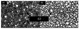
도 4는 도 2의 전도성 잉크에 용해된 유기 금속 화합물로부터 금속 입자들(nano-cluster)이 추출되었을 때 고분자 물질의 유무에 따라 도전패턴과 절연패턴이 형성되는 과정을 도시한 도면이고,
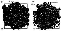
도 5는 도 2의 열처리단계 이후의 전도성 잉크로부터 추출된 금속 입자(nano-cluster)가 고분자 물질 사이에 이격되게 배치되어 있는 것을 도시한 도면이고,
도 6은 도 2의 열처리단계 이후의 도전 패턴의 표면저항(a)과 절연 패턴의 표면저항(b)을 측정하여 그래프로 도시한 도면이다.
이하, 본 발명에 따른 표면개질된 마스크 템플릿을 이용한 미세 도전패턴 형성방법의 실시예들을 첨부된 도면을 참조하여 상세히 설명한다.
도 2는 본 발명의 일 실시예에 따라 소수성 물질로 표면개질된 고분자 물질로 형성된 마스크 템플릿을 이용한 미세 도전패턴 형성방법을 순서적으로 도시한 도면이고, 도 3은 에메랄딘 형태의 폴리아닐린이 페르니그라닐린 형태의 폴리아닐린으로 산화되는 과정의 화학식을 도시한 것이고, 도 4는 도 2의 전도성 잉크에 용해된 유기 금속 화합물로부터 금속 입자들(nano-cluster)이 추출되었을 때 고분자 물질의 유무에 따라 도전패턴과 절연패턴이 형성되는 과정을 도시한 도면이고, 도 5는 도 2의 열처리단계 이후의 전도성 잉크로부터 추출된 금속 입자(nano-cluster)가 고분자 물질 사이에 이격되게 배치되어 있는 것을 도시한 도면이고, 도 6은 도 2의 열처리단계 이후의 도전 패턴의 표면저항(a)과 절연 패턴의 표면저항(b)을 측정하여 그래프로 도시한 도면이다.
도 2 내지 도 6을 참조하면, 본 실시예의 표면개질된 마스크 템플릿을 이용한 미세 도전패턴 형성방법은, 고분자 물질 적층단계(S10)와, 소수성 물질 도포단계(S20)와, 마스크 템플릿 형성단계(S30)와, 잉크 적층단계(S40)와, 열처리단계(S50)를 포함한다.
상기 고분자 물질 적층단계(S10)에서는, 고분자(20) 물질을 기판(10)의 상측에 적층한다. 고분자 물질(20)의 적층은 원심력을 이용하여 물질을 도포하는 스핀코팅(spin-coating) 또는 슬릿코팅과 같은 코팅방식을 이용하거나, 롤코터, 스크린 프린팅과 같은 인쇄방식에 의한다. 본 실시예에서는 스핀코터(spin-coater)의 회전수를 500rpm으로 설정하여, 20초 동안 기판(10)의 상측에 고분자 물질(20)을 도포한다. 한편 고분자 물질(20)은 스프레이 코팅방식에 의하여 적층될 수도 있다.
본 실시예에서 기판(10)에 적층되는 고분자 물질(20)은, 제조방법이 간단하고 다른 고분자 물질에 비하여 열적 특성이 우수한 폴리아닐린(polyaniline)을 사용하며, 폴리아닐린은 루코-에메랄딘 형태(lecu-emeraldine base), 에메랄딘 형태(emeraldine base) 혹은 페르니그라닐린 형태(pernigraniline base)로 기판(10)에 적층될 수 있다.
에메랄딘 형태의 폴리아닐린은 루코-에메랄딘 형태(leuco-emeraldine base)의 폴리아닐린이 부분적으로 산화된 형태의 물질로써, 전도성을 가지며 녹색을 띈다. 따라서, 기판(10)에 에메랄딘 형태의 폴리아닐린이 적층되면 기판(10)은 전체적으로 녹색을 띈다.
기판(10)에 폴리아닐린을 적층한 후에 이를 170℃에서 5분간 가열하여 폴리아닐린에 잔존하는 유기용매를 제거함과 동시에 폴리아닐린의 유기용매에 대한 내성을 증가시키도록 한다.
상기 소수성 물질 도포단계(S20)에서는, 소수성 물질(30) 물질을 고분자 물질(20)의 상측에 도포한다. 소수성 물질(30)의 도포는 고분자 물질(20)의 적층과 마찬가지로 원심력을 이용하여 물질을 도포하는 스핀코팅(spin-coating) 또는 슬릿코팅과 같은 코팅방식을 이용하거나, 롤코터, 스크린 프린팅과 같은 인쇄방식에 의한다. 본 실시예에서는 스핀코터(spin-coater)의 회전수를 500rpm으로 설정하여, 20초 동안 고분자 물질(20)의 상측에 소수성 물질(30)을 도포한다. 한편 소수성 물질(30)은 스프레이 코팅방식에 의하여 적층될 수도 있다.
본 실시예에서 고분자 물질(20) 상에 도포되는 소수성 물질(30)로는, 불소를 함유한 하이드로 카본 계통이 광범위하게 사용될 수 있으며, 일례로써 3M사의 SRC-220 혹은 Cytonix사의 FluoroPel과 같은 화합물 등이 이용될 수 있다.
소수성 물질(30) 물질이 고분자 물질(20) 상에 도포된 후, 소수성 물질(30)은 고분자 물질(20) 내부로 침투한다. 따라서 본 실시예에서는 소수성 물질(30)이 고분자 물질(20) 상에서 하나의 층으로 코팅된 형태가 아니라, 소수성 물질(30)이 고분자 물질(20) 내부의 구석구석으로 침투하여 고분자 물질(20) 전체적으로 소수성을 가지도록 변화되는 형태를 가진다. 본 명세서에서 소수성 성질을 가지도록 변화된 고분자 물질을 부재번호 21로 표시한다.
상기 마스크 템플릿 형성단계(S30)에서는, 기판(10)에 폴리아닐린을 적층하고 그 위에 소수성 물질(30)을 도포한 후, 적층된 폴리아닐린의 상측에서 532nm의 파장대를 가지는 레이저를 조사하여 폴리아닐린의 일부를 제거한다. 폴리아닐린이 제거되면 마스크 템플릿(40)이 형성되는데, 마스크 템플릿(40)은 기판(10)의 일부 영역을 외부에 노출시키는 함몰부(42)와, 기판(10)의 다른 영역을 덮는 소수성의 고분자 물질(21)을 포함한다. 여기서, 레이저는 기판(10)을 훼손하지 않으면서, 고분자 물질(21)을 용이하게 제거할 수 있다면 특정 파장대에 국한되지 않는다.
상기 잉크 적층단계(S40)에서는, 마스크 템플릿(40) 상에 전도성 잉크(50)를 도포한다. 본 실시예에서는 잉크젯 인쇄법을 이용하여 마스크 템플릿(40) 상에 전도성 잉크(50)를 적층한다. 전도성 잉크(50)를 토출하는 노즐부(미도시)가 함몰부(42)의 경로와 일치되어 함몰부(42) 하측의 기판(10) 영역에만 전도성 잉크(50)를 도포하는 것이 바람직하겠지만, 노즐부를 구동하는 구동장치의 오차, 노즐부의 액적토출조건의 변화 등의 요인에 의해 전도성 잉크(50)는 함몰부(42) 하측의 기판(10) 영역뿐만 아니라 고분자 물질(21) 상측에도 함께 도포되는 것이 일반적이다.
본 실시예에서 적층되는 전도성 잉크(50)는, 유기용매에 실버와 같은 높은 전도성을 가지는 금속을 함유한 화합물을 용해한 용액 형태의 유기 실버 잉크(organometallic silver compound)로 마련되며, 실버 잉크를 녹이는데 사용되는 유기용매로서는 금속 화합물의 조성에 따라 알코올과 같은 극성용매, 혹은 톨루엔, 크실렌과 같은 비극성 용매가 사용될 수 있다. 본 발명에서 전도성 잉크(50)는 금속을 함유한 화합물인 이상 그 화합물의 구성과 잉크의 조성에 제한되지 않는다.
또한, 하이브리드 타입으로써, 금속 화합물을 용해한 용액에 실버, 구리 등과 같은 금속 입자를 일부 포함시킨 전도성 잉크(50)가 사용될 수 있다.
상기 열처리단계(S50)에서는, 150℃ 내지 350℃ 범위 내의 온도에서 그에 대응되는 최적의 시간 동안 유기 실버 잉크를 가열하여 유기 실버 화합물로부터 금속상의 실버 입자들을 추출한다.
도 2(e)에 도시된 상태에서 열처리단계(S50)를 거치면, 마스크 템플릿(40)의 함몰부(42)와 고분자 물질(21) 영역에서는 서로 다른 변화가 발생한다.
함몰부(42) 영역에서는, 도 2(f)에 도시된 바와 같이, 함몰부(42)를 관통하여 기판(10)의 상측에 도포된 유기 실버 잉크에서 금속 입자들이 추출되고, 추출된 금속 입자들은 서로 응집하여(nano-cluster) 전도성 네트워크를 형성하면서 전기적 전도성을 가지게 된다. 따라서 함몰부(42) 영역 내에 배치되고 전도성 잉크(50)로부터 추출된 금속 입자들은 도전패턴(61)을 형성한다.
고분자 물질(21) 영역에서는, 고분자 물질(21)에 적층된 폴리아닐린 및 유기 실버 잉크에 변화가 일어나게 된다.
도 3을 참조하면, 열처리단계(S50) 이후에는, 에메랄딘 형태의 폴리아닐린은 완전산화(oxidation)되며, 페르니그라닐린 형태(pernigraniline base)의 폴리아닐린으로 변환된다. 이러한 산화는 유기 금속 화합물의 관능단에 의해 촉진될 수 있다. 페르니그라닐린 형태의 폴리아닐린은 비저항이 크므로 전기적 전도성을 갖지 못하고, 색깔은 녹색에서 짙은 푸른색 혹은 검은색으로 바뀐다.
폴리아닐린의 상측에 도포된 유기 실버 잉크는 페르니그라닐린 형태의 폴리아닐린의 내부로 침투하고, 열처리에 의해 유기 실버 잉크로부터 추출된 금속 입자들은 폴리아닐린 사이사이에 배치되어 서로 이격됨으로써 전기적 전도성 네트워크를 형성하지 못한다. 따라서, 응집된 형태에서만 나타날 수 있는 금속 입자들의 전기적 전도성이 발현되지 못하고 전체적으로 전기적인 절연성을 띄며 절연패턴(62)을 형성한다.
도 4 및 도 5를 참조하면, 고분자 물질(20) 상에 적층된 전도성 잉크(50)는 소수성 물질(30)로 표면개질된 고분자 물질(21) 사이의 공극으로 침투한 후 열처리에 의해 금속 입자(63)들로 추출되는데 이들 금속 입자(63)들은 고분자 물질(21)에 의해 이격됨으로써 서로 전기 전도성의 네트워크를 형성하지 못하지만, 기판(10) 상에 적층된 금속 입자(63)들은 서로 응집하여 전기 전도성의 네트워크를 형성한다.
상술한 현상은 본 실시예의 도전패턴과 절연패턴의 각각의 표면저항 값을 측정함으로써 확인할 수 있다. 도 6을 참조하면, 210℃ 온도에서 20분간 열처리한 후 측정된 도전패턴의 표면저항은 2.57±0.06Ω/□ 이고, 절연패턴의 표면저항은 6.01±1.46MΩ/□ 이상으로 측정된다.
상술한 바와 같이 구성된 본 실시예의 표면개질된 마스크 템플릿을 이용한 미세 도전패턴 형성방법은, 마스크 템플릿의 고분자 물질에 소수성 물질을 도포하여 고분자 물질을 표면개질함으로써 추후 도전패턴을 형성하는 전도성 잉크가 충분히 적층되도록 하며, 함몰부에 적층된 전도성 잉크가 고분자 물질 측으로 과량으로 스며들지 않게 함으로써 도전패턴을 형성하게 될 전도성 잉크의 양을 충분하게 유지되도록 함으로써 도전패턴의 전기저항을 감소시키며 패턴의 두께를 일정하게 형성할 수 있는 효과를 얻을 수 있다.
또한 상술한 바와 같이 구성된 본 실시예의 표면개질된 마스크 템플릿을 이용한 미세 도전패턴 형성방법은, 마스크 템플릿 상에 전도성 잉크를 도포하여 고분자 물질 상에 적층된 전도성 잉크는 고분자 물질과 반응하여 절연패턴을 형성하고, 함몰부에 적층된 전도성 잉크는 도전패턴을 형성함으로써, 근접한 도전패턴 간에 잘못 도포된 전도성 잉크로 인한 전기적 합선 불량을 방지할 수 있는 효과를 얻을 수 있다
본 발명의 실시예들에 있어서, 레이저를 이용하여 일부 고분자 물질을 제거함으로써 마스크 템플릿을 형성하였으나, 고분자 물질을 기판 상에 적층한 후 가압, 가열하는 임프린팅 방식을 통하여 마스크 템플릿을 제작할 수도 있다.
본 발명의 실시예들에 있어서, 전도성 잉크로 유기 실버 잉크가 이용되었으나, 미세패턴의 종류에 따라 금, 아연, 백금, 니켈, 구리 등 다양한 금속 화합물이 이용될 수 있으며, 전도성 잉크는 발명의 취지가 훼손되지 않는 한 다양한 적용범위가 있을 수 있다.
본 발명의 권리범위는 상술한 실시예에 한정되는 것이 아니라 첨부된 특허청구범위 내에서 다양한 형태의 실시예로 구현될 수 있다. 특허청구범위에서 청구하는 본 발명의 요지를 벗어남이 없이 당해 발명이 속하는 기술 분야에서 통상의 지식을 가진 자라면 누구든지 변형 가능한 다양한 범위까지 본 발명의 청구범위 기재의 범위 내에 있는 것으로 본다.
마스크 템플릿에서 최종적으로 전기적 절연성을 가지게 되는 고분자 물질 상에 소수성 물질을 도포하여 고분자 물질로 구성된 입자들의 표면을 개질함으로써 함몰부 내에 전도성 잉크를 충분히 적층할 수 있도록 하며, 전도성 잉크가 고분자 물질을 구성하는 입자들 간의 공극으로 스며들어 가는 것을 제어함으로써, 함몰부 내에 도전패턴을 형성하게 될 전도성 잉크의 양을 일정하게 유지할 수 있는 표면개질된 마스크 템플릿을 이용한 미세 도전패턴 형성방법이 제공된다.
Claims (9)
- 기판 상에 고분자 물질을 적층하는 고분자 물질 적층단계;상기 고분자 물질 상에 소수성 물질을 도포하여 상기 고분자 물질 내에 상기 소수성 물질을 침투시키는 소수성 물질 도포단계;상기 고분자 물질 중 일부를 제거하여 상기 기판의 일부 영역을 외부에 노출시키는 함몰부를 형성하는 마스크 템플릿 형성단계;상기 마스크 템플릿 상에 전도성 잉크를 적층하는 잉크 적층단계; 및상기 전도성 잉크 내부에 용해된 금속 화합물로부터 금속 입자를 추출하기 위하여 열을 가하여, 상기 고분자 물질이 도포된 부위는 전기적 절연성을 가지는 절연패턴을 형성하고, 상기 함몰부 내의 전도성 잉크는 상기 금속 입자들이 추출되어 융합됨으로써 전기적 전도성을 가지는 도전패턴을 형성하는 열처리단계;를 포함하는 것을 특징으로 하는 표면개질된 마스크 템플릿을 이용한 미세 도전패턴 형성방법.
- 제1항에 있어서,상기 열처리단계에서,상기 고분자 물질 상에 적층된 전도성 잉크는 상기 고분자 물질 사이의 틈새로 침투하며, 열처리에 의해 상기 전도성 잉크로부터 추출된 금속 입자들이 상기 고분자 물질 내에서 이격되게 배치됨으로써 상기 절연패턴이 전체적으로 전기적 절연성을 가지는 것을 특징으로 하는 표면개질된 마스크 템플릿을 이용한 미세 도전패턴 형성방법.
- 제1항에 있어서,상기 잉크 적층단계에서는, 잉크젯 인쇄법을 이용하여 상기 전도성 잉크를 적층하는 것을 특징으로 하는 표면개질된 마스크 템플릿을 이용한 미세 도전패턴 형성방법.
- 제1항에 있어서,상기 마스크 템플릿 형성단계에서는, 상기 고분자 물질 측에 레이저를 조사하여 상기 고분자 물질 중 일부를 제거하는 것을 특징으로 하는 표면개질된 마스크 템플릿을 이용한 미세 도전패턴 형성방법.
- 제1항에 있어서,상기 마스크 템플릿 형성단계에서는, 임프린팅 방법을 이용하는 것을 특징으로 하는 표면개질된 마스크 템플릿을 이용한 미세 도전패턴 형성방법.
- 제1항에 있어서,상기 열처리단계는,상기 전도성 잉크를 150℃ 내지 350℃의 범위 내에서 가열하는 것을 특징으로 하는 표면개질된 마스크 템플릿을 이용한 미세 도전패턴 형성방법.
- 제1항에 있어서,상기 고분자 물질은 폴리아닐린(polyaniline)인 것을 특징으로 하는 표면개질된 마스크 템플릿을 이용한 미세 도전패턴 형성방법.
- 제1항에 있어서,상기 전도성 잉크는 용액 상태의 유기 금속 화합물인 것을 특징으로 하는 표면개질된 마스크 템플릿을 이용한 미세 도전패턴 형성방법.
- 제8항에 있어서,상기 전도성 잉크는 금속 입자들을 더 포함하는 것을 특징으로 하는 표면개질된 마스크 템플릿을 이용한 미세 도전패턴 형성방법.
Applications Claiming Priority (2)
| Application Number | Priority Date | Filing Date | Title |
|---|---|---|---|
| KR10-2009-0101310 | 2009-10-23 | ||
| KR1020090101310A KR100991103B1 (ko) | 2009-10-23 | 2009-10-23 | 표면개질된 마스크 템플릿을 이용한 미세 도전패턴 형성방법 |
Publications (1)
| Publication Number | Publication Date |
|---|---|
| WO2011049283A1 true WO2011049283A1 (ko) | 2011-04-28 |
Family
ID=43409178
Family Applications (1)
| Application Number | Title | Priority Date | Filing Date |
|---|---|---|---|
| PCT/KR2010/003664 Ceased WO2011049283A1 (ko) | 2009-10-23 | 2010-06-08 | 표면개질된 마스크 템플릿을 이용한 미세 도전패턴 형성방법 |
Country Status (3)
| Country | Link |
|---|---|
| US (1) | US8241712B2 (ko) |
| KR (1) | KR100991103B1 (ko) |
| WO (1) | WO2011049283A1 (ko) |
Families Citing this family (3)
| Publication number | Priority date | Publication date | Assignee | Title |
|---|---|---|---|---|
| CN103325441A (zh) * | 2012-03-21 | 2013-09-25 | 宸鸿科技(厦门)有限公司 | 触控面板之导电薄膜及其制造方法 |
| JP6259695B2 (ja) * | 2014-03-24 | 2018-01-10 | 芝浦メカトロニクス株式会社 | 基板処理装置、基板処理方法及び基板を製造する方法 |
| EP4444065A4 (en) * | 2021-12-03 | 2025-10-22 | Seoul Nat R&Bd Foundation | METHOD FOR FORMING METAL ELECTRODE PATTERN USING PATTERN FORMATION CONTROL MATERIAL, AND SUBSTRATE, ELECTRONIC DEVICE, AND DISPLAY DEVICE HAVING METAL ELECTRODE PATTERN |
Citations (2)
| Publication number | Priority date | Publication date | Assignee | Title |
|---|---|---|---|---|
| US4344817A (en) * | 1980-09-15 | 1982-08-17 | Photon Power, Inc. | Process for forming tin oxide conductive pattern |
| US20040203235A1 (en) * | 2003-01-15 | 2004-10-14 | Seiko Epson Corporation | Formation method for metal element, production method for semiconductor device, production method for electronic device, semiconductor device, electronic device, and electronic equipment |
Family Cites Families (10)
| Publication number | Priority date | Publication date | Assignee | Title |
|---|---|---|---|---|
| US5882722A (en) * | 1995-07-12 | 1999-03-16 | Partnerships Limited, Inc. | Electrical conductors formed from mixtures of metal powders and metallo-organic decompositions compounds |
| JP3229555B2 (ja) * | 1996-10-15 | 2001-11-19 | 富士通株式会社 | プラズマディスプレイパネル及びその製造方法 |
| SG99865A1 (en) * | 2000-07-04 | 2003-11-27 | Univ Singapore | Photoinduced coversion of polyaniline from an insulating state to a conducting state |
| TW516061B (en) * | 2001-09-12 | 2003-01-01 | Ind Tech Res Inst | Manufacturing method for triode-type electron emitting source |
| GB2413895A (en) | 2004-05-07 | 2005-11-09 | Seiko Epson Corp | Patterning substrates by ink-jet or pad printing |
| JP4876415B2 (ja) * | 2005-03-29 | 2012-02-15 | セイコーエプソン株式会社 | 有機el装置の製造方法、デバイスの製造方法 |
| US7510951B2 (en) * | 2005-05-12 | 2009-03-31 | Lg Chem, Ltd. | Method for forming high-resolution pattern with direct writing means |
| WO2007061115A1 (ja) * | 2005-11-28 | 2007-05-31 | Asahi Glass Company, Limited | 隔壁、カラーフィルタ、有機elの製造方法 |
| JP4478164B2 (ja) * | 2007-03-12 | 2010-06-09 | 株式会社日立ハイテクノロジーズ | 微細構造転写装置、スタンパおよび微細構造の製造方法 |
| KR100969172B1 (ko) | 2009-06-22 | 2010-07-14 | 한국기계연구원 | 마스크 템플릿을 이용한 미세패턴 형성방법 |
-
2009
- 2009-10-23 KR KR1020090101310A patent/KR100991103B1/ko not_active Expired - Fee Related
- 2009-11-12 US US12/616,853 patent/US8241712B2/en not_active Expired - Fee Related
-
2010
- 2010-06-08 WO PCT/KR2010/003664 patent/WO2011049283A1/ko not_active Ceased
Patent Citations (2)
| Publication number | Priority date | Publication date | Assignee | Title |
|---|---|---|---|---|
| US4344817A (en) * | 1980-09-15 | 1982-08-17 | Photon Power, Inc. | Process for forming tin oxide conductive pattern |
| US20040203235A1 (en) * | 2003-01-15 | 2004-10-14 | Seiko Epson Corporation | Formation method for metal element, production method for semiconductor device, production method for electronic device, semiconductor device, electronic device, and electronic equipment |
Also Published As
| Publication number | Publication date |
|---|---|
| US20110097514A1 (en) | 2011-04-28 |
| US8241712B2 (en) | 2012-08-14 |
| KR100991103B1 (ko) | 2010-11-01 |
Similar Documents
| Publication | Publication Date | Title |
|---|---|---|
| KR100991105B1 (ko) | 자기패턴된 전도성 패턴과 도금을 이용한 고전도도 미세패턴 형성방법 | |
| JP4972260B2 (ja) | パターニングされた半導体膜を形成する方法 | |
| CN101068451B (zh) | 布线电路板 | |
| WO2018194414A1 (ko) | 인쇄회로 나노섬유웹 제조방법, 이를 통해 제조된 인쇄회로 나노섬유웹 및 이를 이용한 전자기기 | |
| JP5638565B2 (ja) | ポリマー薄膜における自己整合ビアホールの形成 | |
| KR100969172B1 (ko) | 마스크 템플릿을 이용한 미세패턴 형성방법 | |
| WO2008131392A1 (en) | Intercalated compound | |
| WO2011126347A2 (ko) | 열형 롤 임프린팅과 블레이드 코팅을 이용하는 필름제품 제조방법, 이를 이용한 보안 필름 및 필름 일체형 전기 소자 | |
| KR20140043249A (ko) | 전자 부품의 제조 방법 및 상기 방법으로 제조된 전자 부품 | |
| TWI383503B (zh) | A pattern forming method, a manufacturing method of a semiconductor device, and a semiconductor device | |
| WO2011049283A1 (ko) | 표면개질된 마스크 템플릿을 이용한 미세 도전패턴 형성방법 | |
| US11171179B2 (en) | Memory array, method for manufacturing memory array, memory array sheet, method for manufacturing memory array sheet, and wireless communication apparatus | |
| US8048725B2 (en) | Method of forming pattern and method of producing electronic element | |
| KR20060063903A (ko) | 유기 반도체의 적층법 | |
| JP4760844B2 (ja) | 電子部品の製造方法および該方法で製造された電子部品 | |
| KR100984256B1 (ko) | 자기 정렬 그라비어인쇄를 이용한 중첩정밀도 제어 방법 | |
| TWI237899B (en) | Method for manufacturing OTFT by high precision printing | |
| KR20220089652A (ko) | 전자 컴포넌트를 제조하기 위한 방법 | |
| WO2011037285A1 (ko) | 전극 제조방법 | |
| WO2020153642A1 (ko) | 플렉서블 케이블 점퍼 구조체 및 이를 제조하는 방법 | |
| US20040155188A1 (en) | Infrared sensor and method for making same | |
| US7476603B2 (en) | Printing conductive patterns using LEP | |
| FI121562B (fi) | Menetelmä johteiden ja puolijohteiden valmistamiseksi | |
| WO2013111995A1 (ko) | 다층 인쇄 회로 기판 및 이의 제조 방법 | |
| JP5677266B2 (ja) | パターニングされた半導体膜を形成する方法 |
Legal Events
| Date | Code | Title | Description |
|---|---|---|---|
| 121 | Ep: the epo has been informed by wipo that ep was designated in this application |
Ref document number: 10825108 Country of ref document: EP Kind code of ref document: A1 |
|
| 122 | Ep: pct application non-entry in european phase |
Ref document number: 10825108 Country of ref document: EP Kind code of ref document: A1 |