WO2011027583A1 - 電子装置用配線基板、その製造方法及びタッチパネル - Google Patents
電子装置用配線基板、その製造方法及びタッチパネル Download PDFInfo
- Publication number
- WO2011027583A1 WO2011027583A1 PCT/JP2010/053596 JP2010053596W WO2011027583A1 WO 2011027583 A1 WO2011027583 A1 WO 2011027583A1 JP 2010053596 W JP2010053596 W JP 2010053596W WO 2011027583 A1 WO2011027583 A1 WO 2011027583A1
- Authority
- WO
- WIPO (PCT)
- Prior art keywords
- wiring
- coating layer
- copper alloy
- film
- wiring board
- Prior art date
- Legal status (The legal status is an assumption and is not a legal conclusion. Google has not performed a legal analysis and makes no representation as to the accuracy of the status listed.)
- Ceased
Links
Images



Classifications
-
- G—PHYSICS
- G06—COMPUTING OR CALCULATING; COUNTING
- G06F—ELECTRIC DIGITAL DATA PROCESSING
- G06F3/00—Input arrangements for transferring data to be processed into a form capable of being handled by the computer; Output arrangements for transferring data from processing unit to output unit, e.g. interface arrangements
- G06F3/01—Input arrangements or combined input and output arrangements for interaction between user and computer
- G06F3/03—Arrangements for converting the position or the displacement of a member into a coded form
- G06F3/041—Digitisers, e.g. for touch screens or touch pads, characterised by the transducing means
- G06F3/044—Digitisers, e.g. for touch screens or touch pads, characterised by the transducing means by capacitive means
-
- H—ELECTRICITY
- H05—ELECTRIC TECHNIQUES NOT OTHERWISE PROVIDED FOR
- H05K—PRINTED CIRCUITS; CASINGS OR CONSTRUCTIONAL DETAILS OF ELECTRIC APPARATUS; MANUFACTURE OF ASSEMBLAGES OF ELECTRICAL COMPONENTS
- H05K3/00—Apparatus or processes for manufacturing printed circuits
- H05K3/22—Secondary treatment of printed circuits
- H05K3/24—Reinforcing of the conductive pattern
-
- G—PHYSICS
- G06—COMPUTING OR CALCULATING; COUNTING
- G06F—ELECTRIC DIGITAL DATA PROCESSING
- G06F2203/00—Indexing scheme relating to G06F3/00 - G06F3/048
- G06F2203/041—Indexing scheme relating to G06F3/041 - G06F3/045
- G06F2203/04103—Manufacturing, i.e. details related to manufacturing processes specially suited for touch sensitive devices
-
- G—PHYSICS
- G06—COMPUTING OR CALCULATING; COUNTING
- G06F—ELECTRIC DIGITAL DATA PROCESSING
- G06F3/00—Input arrangements for transferring data to be processed into a form capable of being handled by the computer; Output arrangements for transferring data from processing unit to output unit, e.g. interface arrangements
- G06F3/01—Input arrangements or combined input and output arrangements for interaction between user and computer
- G06F3/03—Arrangements for converting the position or the displacement of a member into a coded form
- G06F3/041—Digitisers, e.g. for touch screens or touch pads, characterised by the transducing means
- G06F3/044—Digitisers, e.g. for touch screens or touch pads, characterised by the transducing means by capacitive means
- G06F3/0445—Digitisers, e.g. for touch screens or touch pads, characterised by the transducing means by capacitive means using two or more layers of sensing electrodes, e.g. using two layers of electrodes separated by a dielectric layer
-
- G—PHYSICS
- G06—COMPUTING OR CALCULATING; COUNTING
- G06F—ELECTRIC DIGITAL DATA PROCESSING
- G06F3/00—Input arrangements for transferring data to be processed into a form capable of being handled by the computer; Output arrangements for transferring data from processing unit to output unit, e.g. interface arrangements
- G06F3/01—Input arrangements or combined input and output arrangements for interaction between user and computer
- G06F3/03—Arrangements for converting the position or the displacement of a member into a coded form
- G06F3/041—Digitisers, e.g. for touch screens or touch pads, characterised by the transducing means
- G06F3/044—Digitisers, e.g. for touch screens or touch pads, characterised by the transducing means by capacitive means
- G06F3/0446—Digitisers, e.g. for touch screens or touch pads, characterised by the transducing means by capacitive means using a grid-like structure of electrodes in at least two directions, e.g. using row and column electrodes
-
- H—ELECTRICITY
- H05—ELECTRIC TECHNIQUES NOT OTHERWISE PROVIDED FOR
- H05K—PRINTED CIRCUITS; CASINGS OR CONSTRUCTIONAL DETAILS OF ELECTRIC APPARATUS; MANUFACTURE OF ASSEMBLAGES OF ELECTRICAL COMPONENTS
- H05K2201/00—Indexing scheme relating to printed circuits covered by H05K1/00
- H05K2201/01—Dielectrics
- H05K2201/0104—Properties and characteristics in general
- H05K2201/0108—Transparent
-
- H—ELECTRICITY
- H05—ELECTRIC TECHNIQUES NOT OTHERWISE PROVIDED FOR
- H05K—PRINTED CIRCUITS; CASINGS OR CONSTRUCTIONAL DETAILS OF ELECTRIC APPARATUS; MANUFACTURE OF ASSEMBLAGES OF ELECTRICAL COMPONENTS
- H05K2201/00—Indexing scheme relating to printed circuits covered by H05K1/00
- H05K2201/03—Conductive materials
- H05K2201/032—Materials
- H05K2201/0326—Inorganic, non-metallic conductor, e.g. indium-tin oxide [ITO]
Definitions
- the present invention relates to an electronic device wiring board provided with circuit wiring on an insulating transparent substrate, a manufacturing method thereof, and a touch panel.
- Patent Document 1 discloses a technique for obtaining a low contact resistance by laminating an ITO film and a copper alloy layer without a barrier metal layer.
- the wiring / electrode part through which the current flows is formed of a Cu alloy film containing a trace amount of at least one element selected from Zn, Mg, Ni, and Mn.
- Patent Document 2 As an example of using without a barrier metal layer, an electrode terminal of a TFT substrate constituting a liquid crystal display device has a conductive layer mainly composed of copper and a manganese oxide covering the conductive layer. Further, it is disclosed that the oxide layer has a structure that is laminated with a transparent electrode, and the laminated portion is in ohmic contact. However, in Patent Documents 1 and 2 described above, a part of the wiring made of a Cu alloy has a contact part with the transparent conductive film, and only an ohmic junction is realized at the contact part to lower the contact resistance. Not.
- Patent Document 1 discloses the resistivity of the wiring electrode film, but it is only the resistance of the Cu alloy thin film itself constituting the wiring portion. That is, in the above Patent Documents 1 and 2, the electrical resistance when the wiring layer is composed of a transparent conductive film and a Cu alloy laminated film, particularly the current flow of the wiring layer made of the laminated film is greatly affected. No mention is made of electrical resistance along the length direction. Of course, in addition to the alloy composition, conditions for lowering the electrical resistance are not disclosed.
- the present invention has been proposed in view of the above, and can reduce the electrical resistance of a laminated film of a Cu alloy film and a transparent conductive film as wiring, and can also reduce power consumption, a manufacturing method thereof, and a method for manufacturing the same
- An object is to provide a touch panel.
- a wiring board for an electronic device including a circuit wiring on an insulating transparent substrate, wherein the circuit wiring includes copper and a trace amount of an additive element.
- the first and second coating layers have different film thicknesses, and the coating layer having a large thickness includes an oxide of an inorganic element capable of forming a transparent oxide conductive film and an oxide of the additional element.
- the concentration of the additive element in the first and second coating layers is higher than the concentration of the additive element in the wiring body.
- a coating layer having a small thickness among the first and second coating layers is the same as the coating layer having a large thickness.
- the composite oxide layer is composed of the above constituent elements.
- the inorganic element is at least one of indium, gallium, tin, and zinc.
- the additive element is at least one of chromium, manganese, vanadium, aluminum, and magnesium.
- the concentration of the additive element and the inorganic element in the coating layer having the large thickness is set to that in the coating layer having the small thickness. To make it higher.
- the sixth invention of the present application is characterized in that, in the wiring board for an electronic device having the above-described configuration, the conductive characteristic at the interface between the wiring body and the thick coating layer exhibits ohmic characteristics. .
- the thick coating layer has a thickness of 5 nm to 50 nm, and the wiring body has a thickness of 100 nm or more.
- the eighth invention of the present application is a touch panel, and is characterized by using the wiring board for electronic devices having the above-described configuration.
- the transparent conductive film made of an oxide of an inorganic element is formed on the insulating transparent substrate. Forming a copper alloy film made of copper containing an additive element on the transparent conductive film, and heat-treating the copper alloy film under a predetermined condition, thereby adding the additive element in the copper alloy film to the copper alloy.
- the copper alloy film is diffused from the film to form a wiring body made of copper and a small amount of the additive element, and two kinds of coating layers made of complex oxide are formed on the outer peripheral side of the wiring body.
- a heat treatment step, and the coating layer is formed by decomposing the transparent conductive film between the wiring body and the insulating transparent substrate, and the insulating transparent substrate. And a thin coating layer that is not in contact with It is characterized in that. (10)
- a copper alloy film made of copper containing an additive element on the insulating transparent substrate in the method of manufacturing a wiring board for an electronic device provided with circuit wiring on an insulating transparent substrate.
- a transparent conductive film made of an oxide of an inorganic element on the copper alloy film Forming a transparent conductive film made of an oxide of an inorganic element on the copper alloy film, and heat-treating the copper alloy film with the copper alloy film by the heat treatment under a predetermined condition.
- the copper alloy film is diffused from the film to form a wiring body made of copper and a small amount of the additive element, and two kinds of coating layers made of complex oxide are formed on the outer peripheral side of the wiring body.
- a heat treatment step, and the coating layer has a small thickness in contact with the insulating transparent substrate and a coating layer having a large thickness formed by decomposing the transparent conductive film on the copper alloy film. It consists of a certain coating layer.
- An eleventh invention of the present application is the method for manufacturing a wiring board for an electronic device comprising the above steps, wherein each of the two types of coating layers of the large and small thicknesses is made of an inorganic element constituting the transparent conductive film. An oxide and an oxide of the additive element are included. (12) According to a twelfth aspect of the present invention, in the method for manufacturing a wiring substrate for an electronic device comprising the above steps, the inorganic element constituting the transparent conductive film is at least one of indium, gallium, tin, and zinc. To do.
- a thirteenth invention of the present application is the method for manufacturing a wiring board for an electronic device comprising the above steps, wherein the additive element in the copper alloy film has an absolute value of oxide formation energy and the transparent conductive film.
- the absolute value of the oxide formation energy of the inorganic element to be constituted is larger.
- the additive element in the copper alloy film is at least one of chromium, manganese, vanadium, aluminum, and magnesium. It is intended.
- the fifteenth aspect of the present invention is the method for manufacturing a wiring board for an electronic device comprising the above steps, wherein the concentration of the additive element in the copper alloy film is 0.2 at.
- the heat treatment is performed in an air stream comprising an inert gas containing oxygen or in an oxygen atmosphere under reduced pressure. It is performed at a temperature of 150 ° C. or higher and 500 ° C. or lower in an air stream.
- the additive element in the copper alloy film can be diffused from the copper alloy film, so that the wiring body can be made almost similar to pure copper, and the resistance of the wiring body can be greatly reduced.
- the coating layer formed by disassembling the transparent conductive film does not form a clear interface with the wiring body, and the wiring body and the coating layer are electrically continuous. The contact resistance between the two is small. For this reason, the electrical resistance of the laminated film as a whole wiring composed of the wiring main body and the coating layer can be reduced, and the power consumption can be reduced.
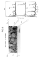
- the additive element of the copper alloy film is 4 at. % Of manganese (Mn), transparent conductive film as ITO film, heat treatment at 300 ° C. for 30 minutes, cross-sectional photograph of laminated film, and energy dispersive X-ray fluorescence analysis (EDX) at each part of the laminated film
- Mn manganese
- ITO film transparent conductive film
- EDX energy dispersive X-ray fluorescence analysis
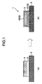
- FIGS. 1A and 1B are diagrams schematically showing a first embodiment of a method of manufacturing a wiring board for an electronic device according to the present invention.
- FIG. 1A shows the first half of the process
- FIG. 1B shows the second half of the process.
- the wiring board 1 for an electronic device according to the present invention is provided with circuit wiring on an insulating transparent substrate 2, and its manufacture is generally performed according to the following procedure. That is, as shown in FIG. 1A, first, a transparent conductive film 3 made of an oxide of an inorganic element is formed on an insulating transparent substrate 2, and then an additive element is formed on the transparent conductive film 3. A copper alloy film 4 made of copper is formed.
- the additive element in the copper alloy film 4 is diffused from the copper alloy film 4 by heat treatment under a predetermined condition, and the copper alloy film 4 is added with a small amount of copper as shown in FIG.
- a wiring body 5 made of an element is formed, and a coating layer 6 made of a complex oxide is formed on the outer peripheral side of the wiring body 5.
- the coating layer 6 includes a coating layer 61 formed by decomposing the transparent conductive film 3 between the wiring body 5 and the insulating transparent substrate 2 and a coating layer 62 that is not in contact with the insulating transparent substrate 2. .
- the additive element in the copper alloy film 4 can be diffused from the copper alloy film 4 so that the wiring body 5 can be made almost pure copper, and the resistance of the wiring body 5 can be greatly reduced. it can.
- the coating layer 61 formed by decomposing the transparent conductive film 3 does not form a clear interface with the wiring body 5, and the wiring body 5 and the coating layer 61 are electrically connected to each other. The contact resistance between the two is small. For this reason, the electrical resistance of the laminated film as the whole wiring composed of the wiring main body 5 and the coating layer 6 can be reduced, and the power consumption can be reduced.
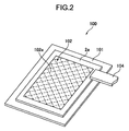
- a display device with an input device 100 includes an image display device 101 as an image generation device, and a panel-like input device that is arranged on the surface of the image display device 101 that emits display light. 102.
- the image display device 101 can use a general liquid crystal panel, an organic EL panel, or the like, and displays a moving image or a still image.
- the input device 102 is a capacitive touch panel, is configured in combination with the image display device 101, and is disposed so as to overlap the viewing side of the image display device 101, that is, the side operated by the user.
- the input device 102 includes a single insulating transparent substrate 2a and a flexible flat cable 104 connected to an end of the insulating transparent substrate 2a.
- a driving circuit (not shown) for detecting the input position in the input device 102 is connected to the flexible flat cable 104.
- an input surface is formed on the upper surface of the insulating transparent substrate 2a, and an area excluding the outer frame portion of the input surface is an input area 102a where input by a fingertip is performed. In this input region 102a, as shown in FIG.
- a plurality of first electrode patterns 11 extending in the direction indicated by the arrow X are formed, and the second electrode pattern extending in the direction indicated by the arrow Y is formed.
- a plurality of rows 12 are formed.
- Each of the first electrode patterns 11 includes diamond-shaped large-area pad portions 11a, 11a,... Arranged in the direction indicated by the arrow X.
- Each of the second electrode patterns 12 includes rhombus-shaped large-area pad portions 12a, 12a,... Arranged in the direction indicated by the arrow Y. Since the first electrode pattern 11 and the second electrode pattern 12 are formed on the same surface of the insulating transparent substrate 2a, the intersection 13 of the first electrode pattern 11 and the second electrode pattern 12 is formed. There are several.
- the first electrode pattern 11 and the second electrode pattern 12 are each formed of a transparent conductive film, and both are electrically insulated at the intersection 13.
- the transparent conductive films forming the pad portions 12 a of the second electrode pattern 12 are connected by the narrow conductive member 14, and the second electrode pattern 12 is indicated by an arrow Y. Electrically connected in the direction.
- the transparent conductive films forming the pad portions 11a that are spaced apart from each other in the first electrode pattern 11 are connected and connected so that another narrow-width conductive member 15 is bridged.
- the electrode pattern 11 is electrically connected in the arrow X direction. Further, in the insulating transparent substrate 2a, in the outer region of the input region 102a, as shown in FIG.
- a plurality of metal wirings electrically connected to each of the first electrode pattern 11 and the second electrode pattern 12 ( Wiring pattern) 70 is formed, and connection terminals 70t for connecting the flexible flat cable 104 are formed on the ends of the metal wirings 70.
- the input device 102 is a capacitive method as described above, and the position thereof is determined by measuring a change in the capacitance between the pads.
- a voltage is sequentially applied to the plurality of first electrode patterns 11 and the plurality of second electrode patterns 12. The user visually recognizes the image displayed on the image display device 101 via the input device 102 and confirms the corresponding input information.
- the metal wiring 70 includes a metal wiring 71 formed on the pad portions 11a and 12a and a metal wiring 72 extending from the metal wiring 71 on the pad portions 11a and 12a to the connection terminal 70t. Consists of.
- the metal wiring 70 is generally manufactured by the procedure shown in FIG. That is, the metal wiring 71 is formed by heat-treating a transparent conductive film that forms the pad portions 11a and 12a on the insulating transparent substrate 2a and a metal thin film made of a copper alloy formed on the transparent conductive film. Is done. At that time, the pad portions 11a and 12a are in contact with each other as long as possible so that the contact electrical resistance between them is as small as possible.
- the metal wiring 72 heat-treats a transparent conductive film etched in the same pattern as the metal wiring 72 on the insulating transparent substrate 2a and a metal thin film made of a copper alloy formed on the transparent conductive film.
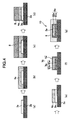
- FIG. 4 is a diagram for more specifically explaining the method of manufacturing the metal wiring formed on the touch panel, and roughly corresponds to the AA cross section and the BB cross section of FIG.
- components that are substantially the same as those in FIG. 1 are denoted by reference numerals obtained by adding a subscript “a” to the reference numerals in FIG. 1.
- a manufacturing method of the metal wiring 70 will be described.
- the electrode patterns 11 and 12 of the input device 102 are also formed at the same time in the patterning of the transparent conductive film, which is a part of the manufacturing process of the metal wiring.
- a process of forming the conductive member 15 at the joint portion of the electrode pad 11a is further added.
- the metal wiring 70 is manufactured in a step of forming a transparent conductive film 3a on the insulating transparent substrate 2a, and the obtained film is patterned by etching.
- a transparent and insulating material such as a resin substrate including glass and a film can be used.
- the transparent conductive film 3a is made of an inorganic oxide, and the inorganic element constituting the transparent conductive film 3a is at least one of indium, gallium, tin, and zinc. Specifically, ITO (Indium Tin Oxide), IZO (Indium Zinc Oxide), or the like can be used, and ITO is preferably used. Film formation methods can be broadly classified into chemical film formation methods such as spray pyrolysis and CVD, and physical film formation methods such as vapor deposition and sputtering.
- a copper alloy film 4a is formed so as to cover the transparent conductive film 3a.
- the copper alloy film 4a is an alloy of copper and an additive element, and the additive element is at least one of chromium, manganese, vanadium, aluminum, and magnesium, and the concentration is 0.2 at. % Or more and 10 at. % Or less. Concentration is 0.2 at. % Or less, the composite oxide 6a is not uniformly formed in the heat treatment process to be described later, and there is a problem because the film thickness becomes thin and adhesion and durability are insufficient.
- the resist film 8 is applied and baked by a conventional method, and thereafter, exposure and development are performed using a conventional method as shown in FIG. Perform patterning. Thereafter, the resist film 8 is peeled off and washed (FIG. 4 (e)), and a heat treatment under a predetermined condition is performed on the laminate composed of the insulating transparent substrate 2a, the transparent conductive film 3a, and the copper alloy film 4a.
- a coating layer 6a made of a complex oxide is formed on the outer peripheral side (FIG. 4 (f)).
- the coating layer 6a has a large coating layer 61a formed by disassembling the transparent conductive film 3a between the wiring body 5a and the insulating transparent substrate 2a, and a small thickness not in contact with the insulating transparent substrate 2a. It consists of a certain coating layer 62a.
- the laminated film composed of the wiring body 5a and the coating layer 6a is covered with a protective film 9 made of silicon dioxide.
- the input device wiring substrate (electronic device wiring substrate) 10 including the metal wiring 70 including the wiring body 5a and the coating layer 6a as the circuit wiring is manufactured on the insulating transparent substrate 2a.
- the transparent conductive film 3a is patterned before the copper alloy film 4a is laminated.
- this patterning can be performed by selecting an appropriate etching solution.
- two layers may be sequentially performed in FIG. 4D of the process.
- the above heat treatment has an oxygen partial pressure of 10 -4 Pa or more, 10 -1 It is performed in an atmosphere of Pa or lower.
- Oxygen partial pressure is 10 -4 If it is less than Pa, the additive element is not sufficiently oxidized and remains in the wiring body 5a, so that the resistance does not decrease, and the oxygen partial pressure is 10%. -1 When it is larger than Pa, there is a problem that the copper itself constituting the wiring body is oxidized and the resistance is increased. Even within the above range, the lower limit is 10 -3 More than Pa is more suitable.
- the above heat treatment may be performed in an air stream composed of an inert gas containing oxygen as long as the oxygen partial pressure condition is satisfied. For example, the total pressure is 1 atm (10 5 Pa), the oxygen concentration in the inert gas is 0.01 ppm (oxygen partial pressure 10 -3 Pa) to 1 ppm (oxygen partial pressure 10) -1 Pa).
- the oxygen concentration is 0.001 ppm (10 -4
- the effect of the present invention is obtained if it is greater than or equal to (Pa), but in the range of 0.001 to 0.01 ppm, the additive element does not oxidize sufficiently and remains in the wiring body 5a. Is slightly inferior. If the concentration is higher than 1 ppm, the copper itself constituting the wiring body is oxidized and the resistance increases. Further, the heat treatment is performed at a temperature of 150 ° C. or higher and 500 ° C. or lower. If the heat treatment temperature is 150 ° C.
- the additive element of the copper alloy film 4a does not sufficiently react with the transparent conductive film 3a, and at the same time, the additive element of the copper alloy film 4a does not react with oxygen, and as a result, a uniform coating layer There arises a problem that 6a is not formed.
- the heat treatment temperature is 500 ° C. or higher, the copper alloy film 4a is oxidized and the resistance increases.
- the additive element in the copper alloy film 4a is such that the absolute value of the oxide formation energy (having a negative value) is larger than the absolute value of the oxide formation energy of the inorganic element constituting the transparent conductive film 3a. Is used.
- the oxide formation energy is a standard free energy change for forming an oxide, and indicates an energy reduction amount when a single element is oxidized.
- the oxide formation energy when oxidation of a substance takes a negative value, and the greater the absolute value of this negative value, the stronger the oxidation tendency.
- the additive element in the copper alloy film 4a easily escapes to the periphery of the transparent conductive film 3a and the like, and diffusion from the copper alloy film 4a becomes easy.
- the copper alloy film 4a becomes a wiring body 5a made of pure copper and a trace amount of additive elements, and a coating layer 6a made of a complex oxide is formed on the outer peripheral side of the wiring body 5a.
- the resistance of the wiring body 5a is reduced.
- the coating layer 61a formed by decomposing the transparent conductive film 3a does not form a clear interface with the wiring body 5, and the wiring body 5a and the coating layer 61a are electrically connected to each other.
- the contact resistance between the two is small.
- the electrical resistance of the laminated film as a whole wiring composed of the wiring main body 5a and the coating layer 61a can be reduced.
- the conductive characteristics at the interface between the wiring body 5a and the thick coating layer 61a showed ohmic characteristics.
- the wiring body 5a formed by the above heat treatment had a film thickness of 100 nm or more and 1000 nm or less.
- the coating layer 61a formed by decomposing the transparent conductive film 3a has a larger film thickness than the coating layer 62a not in contact with the insulating transparent substrate 2a.
- the coating layer 62a having a small thickness is composed of the same constituent elements as the coating layer 61a having a large thickness. Both included oxides of inorganic elements constituting the transparent conductive film 3a and oxides of additive elements contained in the copper alloy film 4a.
- the additive element contained in the copper alloy film 4a is diffused not only on the transparent conductive film 3a side but also in a wide surrounding area, so that the additive element also escapes from the copper alloy film 4a in the thin coating layer 62a. I found out that it contributed.
- the coating layer 62a having a small thickness contains an oxide of an inorganic element constituting the transparent conductive film 3a, for example, indium oxide. This is because the coating layer 62a is only an oxide of an additive element. It is presumed that the effect of improving the chemical resistance and corrosion resistance of the surface of the metal wiring 70 is exhibited more than the case.
- the metal wiring 70 of samples 1 to 4 is manufactured using manganese (Mn) as the additive element of the copper alloy film 4a and using the transparent conductive film 3a as the ITO film (inorganic elements are indium (In) and tin (Sn)).
- Mn manganese
- ITO film inorganic elements are indium (In) and tin (Sn)
- Table 1 the resistivity of the metal wiring 70 is a value that can be regarded as a physical property value as a material of the metal wiring 70 (circuit wiring composed of the wiring main body 5a and the coating layer 6a), and the electrical resistance along the length direction is represented by This is a standard for calculation.
- Samples 1 to 4 show the Mn concentration in the copper alloy film 4a, the film thickness of the copper alloy film 4a ("Cu-Mn"), the film thickness of the transparent conductive film 3a (“ITO”), and the heat treatment conditions.
- the results of measuring the resistivity of the laminated films of Samples 1 to 4 after heat treatment by the four-terminal method are shown in the column (4) of Table 1.
- a film obtained by individually heat-treating the copper alloy (Cu-Mn) film 4a and the transparent conductive film (ITO) 3a according to the heat treatment conditions in the column (3) is simply laminated.
- Column (6) of Table 1 shows the resistivity of the structured wiring layer, that is, the resistivity obtained by calculation for the laminated film in which the composite oxide of the present invention is not formed. Note that the value in column (6) assumes that the Cu—Mn film and the ITO film form a parallel circuit, and each film thickness value shown in column (5) and each film value shown in column (5). This is a value obtained by applying the resistivity value to the definition equation of electrical resistivity.
- the column (5) is attached
- ( * ) 1 is an actual measurement value when heat treatment is performed individually according to the heat treatment conditions in column (3).
- ( * ) 2 is an estimated value, but the lowest value in the actual results is adopted, and the calculated value shown in the column (6) is considered to be the minimum value in the realizable range.
- the contact resistivity of the metal wiring 70 represents a resistance in a direction (stacking direction) perpendicular to the length direction of the metal wiring 70 (circuit wiring composed of the wiring body 5a and the coating layer 6a).
- Samples 5 to 7 have a Mn concentration in the copper alloy film 4a constant of 4 atomic%, a constant film thickness, etc., and a laminated film (metal wiring) formed by changing only the heat treatment conditions.
- Sample 5 has an oxygen partial pressure of 1.0 ⁇ 10 10 when heat treatment is not performed on the laminated film.
- sample 7 had an oxygen partial pressure of 1.0 ⁇ 10 -3
- This is a laminated film when heat treatment is performed at 300 ° C. for 0.5 hour at Pa.
- Table 2 the contact resistivity decreases with the heat treatment, and decreases in the order of Sample 6 and Sample 7.
- Sample 7 shows a value one digit smaller than sample 6. The main reason why the contact resistivity of the sample 7 is greatly reduced in this way is that the heat treatment at 300 ° C.
- the additive element of the copper alloy film 4a is changed to 8 at. % Of manganese (Mn)
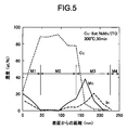
- the transparent conductive film 3a is an ITO film (inorganic elements are indium (In) and tin (Sn)), and the heat treatment is performed at 300 ° C. for 30 minutes. Distribution measurement results will be described with reference to FIG. In FIG. 5, the horizontal axis represents the distance (nm) from the surface of the laminated film, and the vertical axis represents the concentration (%). According to the depth from the surface, the region M1 in FIG.
- the coating layer 62a is the coating layer 62a
- the region M2 is the wiring body 5a
- the region M3 is the coating layer 61a
- the region M4 is the insulating transparent substrate 2a.
- the wiring body 5a region M2
- almost only copper (Cu) is present
- the coating layer 61a region M3 formed by decomposing the ITO film
- Mn, In, and Cu are present in the coating layer 62a (region M1) that is not in contact with the insulating transparent substrate 2a.
- the concentrations of Mn and In are higher than those of Mn and In in the coating layer 61a. It is a low level.
- the wiring main body 5a contains almost only copper (Cu), and the coating layer 62a on the surface has Mn and Cu from the copper alloy film 4a, In from the transparent conductive film 3a, and an insulating transparent substrate.
- Si exists as an oxide, and a layer made of a complex oxide is formed in the same manner as the coating layer 61a.
- the concentrations of Mn, Cu, In, and Si are lower than those in the coating layer 61a.
- FIG. 7A shows the first half of the process
- FIG. 7B shows the second half of the process.
- the second embodiment is different from the first embodiment in that the copper alloy film 40 is formed before the transparent conductive film 30.
- the electronic device wiring board 1a according to the second embodiment of the present invention is provided with circuit wiring on an insulating transparent substrate 20, and its manufacture is generally performed according to the following procedure. That is, as shown in FIG. 7A, first, a copper alloy film 40 made of copper containing an additive element is formed on the insulating transparent substrate 20, and then an inorganic element is formed on the copper alloy film 40. A transparent conductive film 30 made of an oxide is formed.
- the coating layer 60 includes a coating layer 610 having a large thickness formed by decomposing the transparent conductive film 30 on the copper alloy film 40 and a coating layer 620 having a small thickness in contact with the insulating transparent substrate 20. Become.
- the additive element in the copper alloy film 40 is diffused from the copper alloy film 40, so that the wiring body 50 can be made substantially close to pure copper, and the resistance of the wiring body 50 is greatly increased. Can be small. Further, the coating layer 610 formed by decomposing the transparent conductive film 30 does not form a clear interface with the wiring body 50, and the wiring body 50 and the coating layer 610 are electrically connected to each other. The contact resistance between the two is small. For this reason, the electrical resistance of the laminated film as the whole wiring composed of the wiring main body 50 and the coating layer 610 can be reduced, and the power consumption can be reduced.
- FIG. 8 is a diagram for explaining a more specific manufacturing method according to the second embodiment.
- FIG. 8A components that are substantially the same as those in FIG. 7 are denoted by reference numerals obtained by adding a subscript “a” to the reference numerals in FIG. 7.
- the metal wiring 70 is manufactured in a step of forming a copper alloy film 40a on the insulating transparent substrate 20a, and the obtained film is patterned by etching.
- a transparent conductive film 30a is formed so as to cover the copper alloy film 40a. Subsequently, as shown in FIG.
- a resist film 80 is applied and baked, and thereafter, exposure and development are performed and patterning is performed by etching as shown in FIG. 8D. Thereafter, the resist film 80 is peeled off and washed (FIG. 8E), and a heat treatment under a predetermined condition is performed on the laminate including the insulating transparent substrate 20a, the copper alloy film 40a, and the transparent conductive film 30a. By this heat treatment, the additive element in the copper alloy film 40a diffuses from the copper alloy film 40a, and the copper alloy film 40a becomes the wiring body 50a made of copper and a very small amount of the additive element. A coating layer 60a made of a complex oxide is formed on the outer peripheral side (FIG. 8 (f)).
- the coating layer 60a has a large coating layer 610a formed by decomposing the transparent conductive film 30a on the side in contact with the copper alloy film 40a, and a small thickness around the copper alloy film that is not in contact with the transparent conductive film 30a. It consists of a certain coating layer 620a.
- the laminated film composed of the wiring body 50a and the coating layer 60a is covered with a protective film 90 made of silicon dioxide.
- the input device wiring substrate (electronic device wiring substrate) 10a including the metal wiring 70a including the wiring body 50a and the coating layer 60a as the circuit wiring is manufactured on the insulating transparent substrate 20a.
- the electrical resistance of the laminated film as a whole wiring is reduced, and the conductive characteristics at the interface between the wiring main body and the thick coating layer are high. It was able to exhibit various effects such as showing ohmic characteristics and improving chemical resistance and corrosion resistance of the surface of the metal wiring.
- the additive element in the copper alloy film can be diffused from the copper alloy film to make the wiring body almost close to pure copper, and the resistance of the wiring body can be greatly reduced. Can do.
- the coating layer formed by disassembling the transparent conductive film does not form a clear interface with the wiring body, and the wiring body and the coating layer are electrically continuous. The contact resistance between the two is small.
- the wiring board for electronic devices of this invention reduces the electrical resistance of the laminated film of Cu alloy film and transparent conductive film as wiring compared with the wiring board for conventional electronic devices. Therefore, this invention can provide the wiring board for electronic devices excellent in power saving performance, its manufacturing method, and a touch panel.
Landscapes
- Engineering & Computer Science (AREA)
- General Engineering & Computer Science (AREA)
- Theoretical Computer Science (AREA)
- Human Computer Interaction (AREA)
- Physics & Mathematics (AREA)
- General Physics & Mathematics (AREA)
- Manufacturing & Machinery (AREA)
- Microelectronics & Electronic Packaging (AREA)
- Position Input By Displaying (AREA)
- Devices For Indicating Variable Information By Combining Individual Elements (AREA)
- Liquid Crystal (AREA)
- Laminated Bodies (AREA)
Abstract
本発明は、絶縁性透明基板(2)上に回路配線を備えた電子装置用配線基板(1)において、回路配線は、銅と微量の添加元素とからなる配線本体(5)と、配線本体(5)の外周側に形成された、絶縁性透明基板に接している第1の被膜層(61)と、絶縁性透明基板に接していない第2の被膜層(62)とを有し、第1および第2の被膜層61,62は、膜厚みが異なるとともに、厚み大である被膜層(61)は、透明な酸化物導電膜を形成しうる無機元素の酸化物と、添加元素の酸化物とを含む複合酸化物であり、第1および第2の被膜層(61),(62)中の添加元素の濃度は、配線本体(5)中の添加元素の濃度よりも高い、ことを特徴としている。
Description
本発明は、絶縁性透明基板上に回路配線を備えた電子装置用配線基板、その製造方法及びタッチパネルに関するものである。
近年、液晶ディスプレイ、PDP(プラズマディスプレイパネル)、有機ELディスプレイ等の表示装置や、その表示装置と組み合わせて使用されるタッチパネルは、画面が大型化しており、且つ微細化によって配線も細くなり、それに伴って配線の電気抵抗低減に対する要求が高まっている。
これらの表示装置やタッチパネルには、必須の要素として透明導電膜が使用されている。この透明導電膜に配線を形成する場合、従来からAl合金が用いられてきたが、最近、Al合金に比べて電気抵抗が低いCu合金が注目されている。しかし、このCu合金は表面が酸化しやすいため、これを用いる場合にはCu合金と透明導電膜との界面にバリアメタル層を設ける等、何らかの酸化対策が必要であった。
一方、透明導電膜を酸化インジウム錫(ITO)で形成し、そのITO膜上にバリアメタル層を設けずにCu合金配線を形成するようにした技術も提供され、その従来例として、例えば下記の特許文献1,2が知られている。
[特許文献1]
特許文献1には、バリアメタル層なしでITO膜と銅合金層を積層し、低いコンタクト抵抗を得る技術が開示されている。この場合、電流が流れる配線・電極部は、Zn、Mg、Ni、Mnから選ばれる少なくとも1種の元素を微量含有したCu合金膜で形成されている。
[特許文献2]
また、特許文献2には、同様にバリアメタル層なしで用いる例として、液晶表示装置を構成するTFT基板の電極端子が、銅を主体とした導電層と、当該導電層を被覆する、酸化マンガンを主成分とする酸化物層とからなり、さらに、当該酸化物層は、透明電極との積層となる構造を有し、当該積層部がオーミック接合であることが開示されている。
しかし、上記の特許文献1、2では、Cu合金からなる配線の一部が透明導電膜との接触部を有する構成であり、その接触部でオーミック接合を実現し接触抵抗を下げることしか考慮されていない。特許文献1では配線電極膜の抵抗率を開示しているが、あくまで配線部を構成するCu合金薄膜自体の抵抗である。
すなわち、上記の特許文献1、2において、配線層が透明導電膜とCu合金の積層膜とから構成される場合の電気抵抗、特に積層膜からなる配線層の、電流の流れに対して影響大となる長さ方向に沿った電気抵抗については何ら言及されていない。当然、合金組成以外に、電気抵抗を下げるための条件についても開示されていない。
この発明は上記に鑑み提案されたもので、配線としてのCu合金膜と透明導電膜の積層膜の電気抵抗を低減し、消費電力も低減することができる電子装置用配線基板、その製造方法及びタッチパネルを提供することを目的とする。
(1)上記目的を達成するために、本願の第1の発明は、絶縁性透明基板上に回路配線を備えた電子装置用配線基板において、前記回路配線は、銅と微量の添加元素とからなる配線本体と、前記配線本体の外周側に形成された、前記絶縁性透明基板に接している第1の被膜層と、前記絶縁性透明基板に接していない第2の被膜層と、を有し、前記第1および第2の被膜層は、膜厚みが異なるとともに、厚み大である被膜層は、透明な酸化物導電膜を形成しうる無機元素の酸化物と、前記添加元素の酸化物とを含む複合酸化物であり、前記第1および第2の被膜層中の前記添加元素の濃度は、前記配線本体中の前記添加元素の濃度よりも高い、ことを特徴としている。
(2)本願の第2の発明は、上記構成の電子装置用配線基板において、前記第1および第2の被膜層の内、厚み小である被膜層を、前記厚み大である被膜層と同一の構成元素からなる複合酸化物層とするものである。
(3)本願の第3の発明は、上記構成の電子装置用配線基板において、前記無機元素を、インジウム、ガリウム、スズおよび亜鉛の内の少なくとも1つとするものである。
(4)本願の第4の発明は、上記構成の電子装置用配線基板において、前記添加元素を、クロム、マンガン、バナジウム、アルミニウムおよびマグネシウムの内の少なくとも1つとするものである。
(5)本願の第5の発明は、上記構成の電子装置用配線基板において、前記厚み大である被膜層における前記添加元素と前記無機元素の各濃度を、前記厚み小である被膜層におけるそれより高くするものである。
(6)本願の第6の発明は、上記構成の電子装置用配線基板において、前記配線本体と前記厚み大である被膜層との界面での導電特性を、オーミック特性を示すことを特徴としている。
(7)本願の第7の発明は、上記構成の電子装置用配線基板において、前記厚み大である被膜層を、膜厚が5nm以上で50nm以下とし、前記配線本体を、膜厚が100nm以上で1000nm以下とするものである。
(8)本願の第8の発明は、タッチパネルであって、上記構成の電子装置用配線基板を用いて構成したことを特徴としている。
(9)本願の第9の発明は、絶縁性透明基板上に回路配線を備えた電子装置用配線基板の製造方法において、前記絶縁性透明基板上に、無機元素の酸化物からなる透明導電膜を形成する工程と、前記透明導電膜上に、添加元素を含む銅からなる銅合金膜を形成する工程と、所定条件下での熱処理により、前記銅合金膜中の前記添加元素を当該銅合金膜から拡散させて当該銅合金膜を銅と微量の前記添加元素とからなる配線本体とするとともに、その配線本体の外周側に、複合酸化物からなる厚みの異なる2種の被膜層を形成する熱処理工程と、を有し、前記被膜層は、前記配線本体と前記絶縁性透明基板との間の前記透明導電膜が分解して形成された厚み大である被膜層と、前記絶縁性透明基板に接していない厚み小である被膜層とからなる、ことを特徴としている。
(10)本願の第10の発明は、絶縁性透明基板上に回路配線を備えた電子装置用配線基板の製造方法において、前記絶縁性透明基板上に、添加元素を含む銅からなる銅合金膜を形成する工程と、前記銅合金膜上に、無機元素の酸化物からなる透明導電膜を形成する工程と、所定条件下での熱処理により、前記銅合金膜中の前記添加元素を当該銅合金膜から拡散させて当該銅合金膜を銅と微量の前記添加元素とからなる配線本体とするとともに、その配線本体の外周側に、複合酸化物からなる厚みの異なる2種の被膜層を形成する熱処理工程と、を有し、前記被膜層は、前記銅合金膜上の前記透明導電膜が分解して形成された厚み大である被膜層と、前記絶縁性透明基板に接している厚み小である被膜層とからなる、ことを特徴としている。
(11)本願の第11の発明は、上記工程から成る電子装置用配線基板の製造方法において、前記厚み大、小の2種の被膜層の各々を、前記透明導電膜を構成する無機元素の酸化物と、前記添加元素の酸化物とを含むことを特徴としている。
(12)本願の第12の発明は、上記工程から成る電子装置用配線基板の製造方法において、前記透明導電膜を構成する前記無機元素を、インジウム、ガリウム、スズおよび亜鉛の内の少なくとも1つとするものである。
(13)本願の第13の発明は、上記工程から成る電子装置用配線基板の製造方法において、前記銅合金膜中の前記添加元素を、酸化物形成エネルギーの絶対値が、前記透明導電膜を構成する前記無機元素の酸化物形成エネルギーの絶対値より大きいものとするものである。
(14)本願の第14の発明は、上記工程から成る電子装置用配線基板の製造方法において、前記銅合金膜中の前記添加元素を、クロム、マンガン、バナジウム、アルミニウムおよびマグネシウムの内の少なくとも1つとするものである。
(15)本願の第15の発明は、上記工程から成る電子装置用配線基板の製造方法において、前記銅合金膜中の前記添加元素を、濃度が0.2at.%以上で、10at.%以下とするものである。
(16)本願の第16の発明は、上記工程から成る電子装置用配線基板の製造方法において、前記熱処理を、酸素を含む不活性気体からなる気流中で、または減圧下での酸素雰囲気からなる気流中で、150℃以上500℃以下の温度で行うものである。
本願発明によると、銅合金膜中の添加元素を当該銅合金膜から拡散させ配線本体をほぼ純銅に近いものとすることができ、配線本体の抵抗を大幅に小さくすることができる。また、透明導電膜が分解されて形成された被膜層は、配線本体との間でハッキリとした界面を形成するには至らず、配線本体と被膜層とは、電気的に連続となっており、双方間の接触抵抗は小さい。このため、配線本体と被膜層とからなる、配線全体としての積層膜の電気抵抗を減少させることができ、消費電力を低減することができる。
1,1a 電子装置用配線基板
2,2a,20,20a 絶縁性透明基板
3,3a 透明導電膜
4,4a 銅合金膜
5,5a 配線本体
6,6a 被膜層
8,80 レジスト膜
9,90 保護膜
10,10a 入力装置用配線基板(電子装置用配線基板)
11 第1の電極パターン
11a パッド部
12 第2の電極パターン
12a パッド部
13 交差部分
14,15 導電部材
30,30a 透明導電膜
40,40a 銅合金膜
50,50a 配線本体
60,60a 被膜層
61,61a,610,610a 被膜層(厚み大)
62,62a,620,620a 被膜層(厚み小)
70,70a 金属配線
70t 接続端子
71,72 金属配線
100 表示装置
101 画像表示装置
102 入力装置
102a 入力領域
104 フレキシブルフラットケーブル
先ず、本発明の第1の実施形態を図1~図6を用いて説明する。
[第1の実施形態]
図1は本発明の電子装置用配線基板製造方法の第1の実施形態を概略的に示す図であり、(a)は工程の前半を、(b)は工程の後半をそれぞれ示している。本発明の電子装置用配線基板1は、絶縁性透明基板2上に回路配線を備えたものであり、その製造は、概略下記の手順で行われる。すなわち、図1(a)に示すように、先ず、絶縁性透明基板2上に、無機元素の酸化物からなる透明導電膜3を形成し、次にその透明導電膜3上に、添加元素を含む銅からなる銅合金膜4を形成する。
続いて、所定条件下での熱処理により、銅合金膜4中の添加元素を当該銅合金膜4から拡散させ、図1(b)に示すように、当該銅合金膜4を銅と微量の添加元素とからなる配線本体5とするとともに、その配線本体5の外周側に、複合酸化物からなる被膜層6を形成する。
この被膜層6は、配線本体5と絶縁性透明基板2との間の透明導電膜3が分解して形成された被膜層61と、絶縁性透明基板2に接していない被膜層62とからなる。
この発明によると、銅合金膜4中の添加元素を当該銅合金膜4から拡散させ、配線本体5をほぼ純銅に近いものとすることができ、配線本体5の抵抗を大幅に小さくすることができる。また、透明導電膜3が分解して形成された被膜層61は、配線本体5との間でハッキリとした界面を形成するには至らず、配線本体5と被膜層61とは、電気的に連続となっており、双方間の接触抵抗は小さい。このため、配線本体5と被膜層6とからなる、配線全体としての積層膜の電気抵抗を減少させることができ、消費電力を低減することができる。
[本発明のタッチパネル]
次に、本発明を表示装置の入力装置に適用した場合について、図2~図6を用いて説明する。
図2は本発明を適用した入力装置付き表示装置、すなわち、タッチパネルの構成を模式的に示す説明図、図3はこの入力装置付き表示装置の平面的な構成を模式的に示す説明図である。これらの図において、入力装置付き表示装置100は、画像生成装置としての画像表示装置101と、この画像表示装置101の、表示光を出射する側の面に重ねて配置されたパネル状の入力装置102とを有している。
画像表示装置101は、一般的な液晶パネル、有機ELパネル等を用いることができ、動画や静止画を表示する。
入力装置102は、静電容量型のタッチパネルであり、画像表示装置101と組み合わせて構成され、画像表示装置101の目視側、すなわちユーザーが操作する側に重ねて配設されている。この入力装置102は、1枚の絶縁性透明基板2aと、絶縁性透明基板2aの端部に接続されたフレキシブルフラットケーブル104とを備えている。フレキシブルフラットケーブル104には、入力装置102において入力位置の検出を行うための駆動回路(図示せず)が接続されている。入力装置102においては、絶縁性透明基板2aの上面に入力面が形成され、その入力面の外枠部を除いた領域が指先による入力が行われる入力領域102aになっている。
この入力領域102aには、図3に示すように、矢印Xで示す方向に延在する第1の電極パターン11が複数列形成され、また矢印Yで示す方向に延在する第2の電極パターン12が複数列形成されている。
第1の電極パターン11の各々は、矢印Xで示す方向に配列された菱形形状の大面積のパッド部11a、11a、…を備えている。また、第2の電極パターン12の各々は、矢印Yで示す方向に配列された菱形形状の大面積のパッド部12a、12a、…を備えている。
第1の電極パターン11と第2の電極パターン12とは、絶縁性透明基板2aの同一面上に形成されているため、第1の電極パターン11と第2の電極パターン12との交差部分13が複数、存在している。第1の電極パターン11及び第2の電極パターン12は、それぞれ透明導電膜で形成されており、この交差部分13において両者は電気的に絶縁されている。そして、その交差部分13において、第2の電極パターン12のパッド部12aを形成している透明導電膜同士は、細幅形状の導電部材14で繋がって、第2の電極パターン12は、矢印Y方向に電気的に接続されている。一方、第1の電極パターン11の離間するパッド部11aを形成する透明導電膜同士は、別の細幅形状の導電部材15がブリッジするように配設されて繋がっており、それにより、第1の電極パターン11は、矢印X方向に電気的に接続されている。
また、絶縁性透明基板2aにおいて入力領域102aの外側領域には、図3に示すように、第1の電極パターン11および第2の電極パターン12の各々に電気的に接続する複数の金属配線(配線パターン)70が形成されており、これらの金属配線70の端部には、フレキシブルフラットケーブル104を接続するための接続端子70tが成膜されている。
このような構成の入力装置付き表示装置100において、入力装置102は、上記のように静電容量方式であり、パッド間の静電容量の変化を計測することにより、その位置を判別する。操作時、複数の第1の電極パターン11および複数の第2の電極パターン12に順次、電圧が印加される。ユーザーは画像表示装置101に表示された画像を、入力装置102を介して視認し、対応する入力情報を確認する。そして、画像表示装置101に表示された指示用画像に対応する位置を、入力装置102の入力領域102a上で指等を用いて触れることにより、情報の入力を行う。この時、導電体である指が触れると、入力装置102上に配設された検出電極との間で静電容量を持つようになる。その結果として指で触れた位置の静電容量が低下し、その位置を不図示の検出用駆動回路(検出部)により算出する。このようにして、いずれの箇所に指が触れたかを検出することができる。
次に、本発明に係る金属配線70の製造方法および構成について説明する。
[本発明の電子装置用配線基板の製造方法]
金属配線70は、図3に示すように、パッド部11a、12a上に形成される金属配線71と、そのパッド部11a、12a上の金属配線71から接続端子70tまで延出した金属配線72とから成っている。この金属配線70は、概略、図1に示した手順で製造される。
すなわち、金属配線71は、絶縁性透明基板2a上のパッド部11a、12aを形成する透明導電膜と、その透明導電膜上に成膜された銅合金からなる金属薄膜とを熱処理することによって形成される。その際に、双方間の接触電気抵抗ができるだけ小さくなるように、パッド部11a、12aに可能な限り長く接する構成となっている。
金属配線72は、絶縁性透明基板2a上の、当該金属配線72と同じパターンにエッチングされた透明導電膜と、その透明導電膜上に成膜された銅合金からなる金属薄膜とを熱処理することによって形成される。
図4はタッチパネルに形成される金属配線の製造方法をより具体的に説明するための図で、図3のA−A断面、およびB−B断面に概略対応している。なお、図4において、図1と略同一の構成要素には、図1に付した符号に添え字aを付加した符号を付している。
ここでは、金属配線70の製造方法について説明するが、入力装置102の電極パターン11、12も、この金属配線の製造工程の一部である、透明導電膜のパターニングにおいて同時に形成される。入力装置102の電極パターン11、12では、電極パッド11aのつなぎ部分の導電部材15の形成工程が更に加わることになる。
金属配線70の製造は、先ず図4(a)に示すように、絶縁性透明基板2a上に透明導電膜3aを成膜する工程で開始し、得られた成膜はエッチングによってパターニングされる。
ここで、絶縁性透明基板2aは、ガラス、フィルムを含む樹脂基板などの透明且つ絶縁性の材料を用いることができる。フィルムはその可撓性により、入力装置102の、衝撃による割れに対する強度を高めることができる。
また、透明導電膜3aは無機酸化物からなり、この透明導電膜3aを構成する無機元素は、インジウム、ガリウム、スズおよび亜鉛の内の少なくとも1つである。具体的には、ITO(Indium Tin Oxide)、IZO(Indium Zinc Oxide)等を用いることができ、好ましくはITOを用いる。成膜方法としては、スプレー熱分解法、CVD法等の化学的成膜法と、蒸着法、スパッタリング法等の物理的成膜法とに大別することができる。中でもスパッタリング法は、得られる膜の抵抗値及び透過率の経時変化が少なく、成膜条件の制御が容易であるため、好ましい。
次に、図4(b)に示すように、透明導電膜3aを覆うように銅合金膜4aを成膜する。この銅合金膜4aは、銅と添加元素との合金であり、添加元素は、クロム、マンガン、バナジウム、アルミニウムおよびマグネシウムの内の少なくとも1つであり、濃度が0.2at.%以上で、10at.%以下である。濃度が0.2at.%以下であれば、後述する熱処理過程において複合酸化物6aが均質に形成されない、膜厚が薄くなるために密着性および耐久性が不足する、等の理由で不具合があり、10at.%以上であれば、配線本体5a中に添加元素が残存して抵抗値が十分に低下しないという理由で不具合が生じる。
続いて、図4(c)に示すように、レジスト膜8を常法により塗布して焼成し、その後図4(d)に示すように、常法を用いて露光・現像を行ってエッチングによりパターニングを行う。
その後、レジスト膜8のはく離、洗浄を行い(図4(e))、絶縁性透明基板2a、透明導電膜3a、銅合金膜4aからなる積層体に所定条件下での熱処理を施す。この熱処理によって、銅合金膜4a中の添加元素が当該銅合金膜4aから拡散し、当該銅合金膜4aが銅と極微量の添加元素とからなる配線本体5aとなるとともに、その配線本体5aの外周側に、複合酸化物からなる被膜層6aが形成される(図4(f))。
被膜層6aは、配線本体5aと絶縁性透明基板2aとの間の透明導電膜3aが分解して形成された厚み大である被膜層61aと、絶縁性透明基板2aに接していない厚み小である被膜層62aとからなる。
最後に、図4(g)に示すように、配線本体5aと被膜層6aとからなる積層膜を、二酸化珪素からなる保護膜9で覆う。このようにして、絶縁性透明基板2a上に、配線本体5aと被膜層6aとからなる金属配線70を回路配線として備えた入力装置用配線基板(電子装置用配線基板)10が製造される。
なお、上記の説明では、図4(a)において透明導電膜3aのパターニングを銅合金膜4aの積層前に行うようにしたが、このパターニングは、適当なエッチング液を選択すれば、銅合金膜4aを積層後、工程の図4(d)において、2層を順に行うようにしてもよい。
上記の熱処理は、酸素分圧が10−4Pa以上、10−1Pa以下の雰囲気中で行う。酸素分圧が10−4Pa未満であれば、添加元素が十分に酸化されないで配線本体5a中に残存するため抵抗が減少しないという不具合が発生し、酸素分圧が10−1Paより大きい場合には、配線本体を構成する銅自体が酸化されて抵抗が上昇するという不具合が生じる。上記範囲内でも、下限側は10−3Pa以上が更に好適である。
上記の熱処理は、酸素分圧の条件が満足されていれば、酸素を含む不活性気体からなる気流中で行ってもよい。例えば全圧が1気圧(105Pa)の不活性気体中の酸素濃度は、0.01ppm(酸素分圧10−3Pa)~1ppm(酸素分圧10−1Pa)の範囲とする。酸素濃度が0.001ppm(10−4Pa)以上であれば本発明の効果を奏するが、0.001から0.01ppmの範囲では、添加元素が十分に酸化されないで配線本体5a中に残存するため、抵抗減少の効果は他の場合よりも若干劣る。1ppmより大きい濃度であれば、配線本体を構成する銅自体が酸化されて抵抗が上昇するという不具合が生じる。
また、上記の熱処理は、150℃以上500℃以下の温度で行う。熱処理温度が150℃以下であれば、銅合金膜4aの添加元素が透明導電膜3aと十分に反応せず、同時に銅合金膜4aの添加元素が酸素と反応せず、その結果均質な被膜層6aを形成しないという不具合が生じる。一方、熱処理温度が500℃以上であれば、銅合金膜4aが酸化されてしまい抵抗が上昇するという不具合が生じる。
本発明では、銅合金膜4a中の添加元素は、酸化物形成エネルギー(負の値となる)の絶対値が、透明導電膜3aを構成する無機元素の酸化物形成エネルギーの絶対値より大きいものが使用されている。ここで、酸化物形成エネルギーとは、酸化物形成のための標準自由エネルギー変化であり、単体元素が酸化されるときのエネルギー減少量を示す。物質の酸化が生じるときの酸化物形成エネルギーは負の値になり、この負の値の絶対値が大きいほど酸化傾向が強い。このため、熱処理時に、銅合金膜4a中の添加元素が透明導電膜3a等の周囲に抜けやすくなり、当該銅合金膜4aからの拡散が容易となる。その結果、銅合金膜4aが純銅と極微量の添加元素とからなる配線本体5aとなるとともに、その配線本体5aの外周側に、複合酸化物からなる被膜層6aが形成される。したがって、配線本体5aの抵抗が小となる。また、透明導電膜3aが分解して形成された被膜層61aは、配線本体5との間でハッキリとした界面を形成するには至らず、配線本体5aと被膜層61aとは、電気的に連続となっており、双方間の接触抵抗は小さい。このため、配線本体5aと被膜層61aとからなる、配線全体としての積層膜の電気抵抗を減少させることができた。
また、配線本体5aと厚み大である被膜層61aとの界面での導電特性は、オーミック特性を示した。
上記の熱処理によって形成された配線本体5aは、膜厚が100nm以上で1000nm以下であった。また、被膜層6aのうち、透明導電膜3aが分解して形成された被膜層61aは、絶縁性透明基板2aに接していない被膜層62aと比較して膜厚が大であり、その膜厚は5nm以上で50nm以下であった。
そして、厚み大、小の2種の被膜層61a、62aのうち、厚み小である被膜層62aは、厚み大である被膜層61aと同一の構成元素からなり、双方の被膜層61a、62aは何れも、透明導電膜3aを構成する無機元素の酸化物と、銅合金膜4aに含まれる添加元素の酸化物とを含んでいた。したがって、銅合金膜4aに含まれる添加元素は、透明導電膜3a側だけでなく、周囲の広い範囲で拡散しており、厚み小の被膜層62aも添加元素が銅合金膜4aから抜けることに貢献していることが分かった。
また、厚み小である被膜層62aには、透明導電膜3aを構成する無機元素の酸化物、例えば酸化インジウムが存在しており、このことは、被膜層62aが添加元素の酸化物のみである場合よりも、金属配線70の表面の耐薬品性、耐腐食性を向上させる効果を発揮していると推測される。
次に、銅合金膜4aの添加元素をマンガン(Mn)とし、透明導電膜3aをITO膜(無機元素がインジウム(In)とスズ(Sn))として、サンプル1~4の金属配線70を製造した場合の、各サンプルの抵抗率の測定結果について、表1を用いて説明する。ここで、金属配線70の抵抗率とは、金属配線70(配線本体5aと被膜層6aとからなる回路配線)の材料としての物性値とみなせる値であり、長さ方向に沿った電気抵抗を算出する場合の基準となる。
表1において、サンプル1~4は、銅合金膜4a中のMn濃度、銅合金膜4aの膜厚(“Cu−Mn”)、透明導電膜3aの膜厚(“ITO”)、および熱処理条件を欄(3)の熱処理条件に従ってそれぞれ変えて形成された積層膜(金属配線)である。上記のサンプル1~4の積層膜の熱処理後の抵抗率を四端子法で測定した結果が、表1の欄(4)に示されている。また、上記サンプル1~4に対して比較するため、銅合金(Cu−Mn)膜4aと透明導電膜(ITO)3aを欄(3)の熱処理条件に従って個別に熱処理した膜が単に積層されて構成された配線層の抵抗率、即ち本発明の複合酸化物が形成されていない積層膜について計算して得られた抵抗率を表1の欄(6)に示している。尚、欄(6)の値は、Cu−Mn膜及びITO膜が並列回路を形成するとみなし、欄(2)に示された各膜厚の値と、欄(5)に示された各膜の抵抗率の値を電気抵抗率の定義式に適用して得られた値である。表1中、欄(5)に付した(*)1は、欄(3)の熱処理条件に従って個別に熱処理した場合の実測値である。(*)2は推測値であるが、実績中の最も低い値を採用しており、欄(6)に示された計算値は実現可能な範囲の最小値と考えられる。
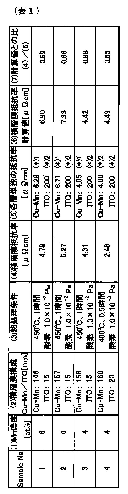
この欄(4)の実測値と欄(6)の計算値とを比較すると、欄(7)に示されるように、熱処理後の積層膜(金属配線)の抵抗率が最大で45%と大幅に低減していることが分かる。
これは、銅合金膜4a中のMnを当該銅合金膜4aから拡散させ配線本体5aをほぼ純銅に近いものとすることができたこと、また透明導電膜3aが分解して形成された被膜層61aは、配線本体5aとの間でハッキリとした界面を形成するには至らず、配線本体5aと被膜層61aとは、電気的に一体化し連続となっており、双方間の接触抵抗が小さくなっていることによるものと考えられる。
次に、銅合金膜4aの添加元素をマンガン(Mn)とし、透明導電膜3aをITO膜として、所定の熱処理条件の下で金属配線70を製造した場合の金属配線70の接触抵抗率の測定結果について、表2を用いて説明する。ここで、金属配線70の接触抵抗率とは、金属配線70(配線本体5aと被膜層6aとからなる回路配線)の長さ方向に垂直な方向(積層方向)での抵抗を表わしている。

表2において、サンプル5~7は、銅合金膜4a中のMn濃度を4原子%一定とし、各膜厚等も一定とし、熱処理条件のみ変化させて積層膜(金属配線)を形成されている。尚、サンプル5は、積層膜に熱処理を施さない場合、サンプル6は、酸素分圧1.0×10⁻³Paで、250℃、0.5時間の熱処理を行った場合、サンプル7は、酸素分圧1.0×10⁻³Paで、300℃、0.5時間の熱処理を行った場合における積層膜である。このサンプル5~7の積層膜の接触抵抗率を測定した結果を表2の欄(4)に示している。
この表2において、接触抵抗率は、熱処理によって小さくなり、サンプル6、サンプル7の順で低くなる。サンプル7はサンプル6に対して1桁小さな値を示している。サンプル7の接触抵抗率がこのように大幅に低減した主な理由は、300℃での熱処理により、透明導電膜3aの分解による被膜層61aの形成、および配線本体5aと被膜層61aとの電気的な一体化が確実に行われたことによると考えられる。
次に、銅合金膜4aの添加元素を、8at.%のマンガン(Mn)とし、透明導電膜3aをITO膜(無機元素がインジウム(In)とスズ(Sn))とし、熱処理を300℃、30分として形成した積層膜(金属配線70)の濃度分布の測定結果について、図5を用いて説明する。この図5において、横軸は積層膜表面からの距離(nm)であり、縦軸は濃度(%)である。
表面からの深さに応じて、図5の領域M1は被膜層62a、領域M2は配線本体5a、領域M3は被膜層61a、領域M4は絶縁性透明基板2aとなる。配線本体5a(領域M2)には、ほぼ銅(Cu)のみが存在し、ITO膜が分解して形成された被膜層61a(領域M3)には、MnとInとCuが存在している。また、絶縁性透明基板2aに接していない被膜層62a(領域M1)にも、MnとInとCuとが存在しているが、MnとInの濃度は、被膜層61a中のMnとInより低いレベルとなっている。この濃度分布測定結果から、銅合金膜4a中のMnが当該銅合金膜4aから拡散し配線本体5aがほぼ純銅に近いものとなるとともに、被膜層61a、62aに拡散していることが分かる。また、透明導電膜3a中のInの一部が銅合金膜4aを通り抜けて表面まで拡散し被膜層62aを形成していることが分かる。
次に、銅合金膜4aの添加元素を、4at.%のマンガン(Mn)とし、透明導電膜3aをITO膜(無機元素がインジウム(In)とスズ(Sn))とし、熱処理を300℃、30分として形成した積層膜(金属配線70)の断面写真、およびその積層膜の各部位に対して行ったEDXによる化学成分分析結果について、図6を用いて説明する。この図6において、断面写真からは、透明導電膜(ITO)3aが分解して形成された被膜層61aと、配線本体5aとの間はハッキリとした界面を形成するには至らず、配線本体5aと被膜層61aとは、一体化し連続したものとなっている。一方、化学成分分析結果から、この被膜層61aには、銅合金膜4aからのMn、Cu、透明導電膜3aのIn、および絶縁性透明基板からのSi、Cが酸化物として存在し、複合酸化物からなる層を形成していることが分かる。また、配線本体5aには、ほぼ銅(Cu)のみが存在し、表面の被膜層62aには、銅合金膜4aからのMn、Cu、透明導電膜3aのIn、および絶縁性透明基板からのSiが酸化物として存在し、被膜層61aと同様に、複合酸化物からなる層を形成している。但し、Mn、Cu、In、Siの各濃度は、被膜層61a中のそれらより低いレベルとなっている。
[第2の実施形態]
続いて、本発明の第2の実施形態を図7、図8を用いて説明する。
図7は本発明の電子装置用配線基板製造方法の第2の実施形態を概略的に示す図であり、(a)は工程の前半を、(b)は工程の後半をそれぞれ示している。この第2の実施形態が、上記の第1の実施形態と相違しているのは、銅合金膜40を透明導電膜30より先に成膜する点である。
本発明の第2の実施形態における電子装置用配線基板1aは、絶縁性透明基板20上に回路配線を備えたものであり、その製造は、概略下記の手順で行われる。すなわち、図7(a)に示すように、先ず、絶縁性透明基板20上に、添加元素を含む銅からなる銅合金膜40を形成し、次にその銅合金膜40上に、無機元素の酸化物からなる透明導電膜30を形成する。
続いて、所定条件下での熱処理により、銅合金膜40中の添加元素を当該銅合金膜40から拡散させて当該銅合金膜40を銅と微量の添加元素とからなる配線本体50とするとともに、その配線本体50の外周側に、複合酸化物からなる厚みの異なる2種の被膜層60を形成する。
この被膜層60は、銅合金膜40上の透明導電膜30が分解して形成された厚み大である被膜層610と、絶縁性透明基板20に接している厚み小である被膜層620とからなる。
この第2の実施形態によると、銅合金膜40中の添加元素を当該銅合金膜40から拡散させ、配線本体50をほぼ純銅に近いものとすることができ、配線本体50の抵抗を大幅に小さくすることができる。また、透明導電膜30が分解して形成された被膜層610は、配線本体50との間でハッキリとした界面を形成するには至らず、配線本体50と被膜層610とは、電気的に連続となっており、双方間の接触抵抗は小さい。このため、配線本体50と被膜層610とからなる、配線全体としての積層膜の電気抵抗を減少させることができ、消費電力を低減することができる。
図8は第2の実施形態のより具体的な製造方法を説明するための図である。ここでは、上記の第1の実施形態の場合と同様に、タッチパネルの金属配線を製造する場合について説明する。なお、図8において、図7と略同一の構成要素には、図7に付した符号に添え字aを付加した符号を付している。
金属配線70の製造は、先ず図8(a)に示すように、絶縁性透明基板20a上に銅合金膜40aを成膜する工程で開始し、得られた成膜はエッチングによってパターニングされる。
次に、図8(b)に示すように、銅合金膜40aを覆うように透明導電膜30aを成膜する。
続いて、図8(c)に示すように、レジスト膜80を塗布して焼成し、その後図8(d)に示すように、露光・現像を行ってエッチングによりパターニングを行う。
その後、レジスト膜80の剥離・洗浄を行い(図8(e))、絶縁性透明基板20a、銅合金膜40a、透明導電膜30aからなる積層体に所定条件下での熱処理を施す。この熱処理によって、銅合金膜40a中の添加元素が当該銅合金膜40aから拡散し、当該銅合金膜40aが銅と極微量の添加元素とからなる配線本体50aとなるとともに、その配線本体50aの外周側に、複合酸化物からなる被膜層60aが形成される(図8(f))。
被膜層60aは、銅合金膜40aと接する側の透明導電膜30aが分解して形成された厚み大である被膜層610aと、透明導電膜30aに接していない、銅合金膜周囲の厚み小である被膜層620aとからなる。
最後に、図8(g)に示すように、配線本体50aと被膜層60aとからなる積層膜を、二酸化珪素からなる保護膜90で覆う。このようにして、絶縁性透明基板20a上に、配線本体50aと被膜層60aとからなる金属配線70aを回路配線として備えた入力装置用配線基板(電子装置用配線基板)10aが製造される。
この第2の実施形態においても、上記の第1の実施形態の場合と同様に、配線全体としての積層膜の電気抵抗低減、配線本体と厚み大である被膜層との界面での導電特性がオーミック特性を示すこと、金属配線の表面の耐薬品性、耐腐食性の向上等の諸効果を発揮させることができた。
[第1の実施形態]
図1は本発明の電子装置用配線基板製造方法の第1の実施形態を概略的に示す図であり、(a)は工程の前半を、(b)は工程の後半をそれぞれ示している。本発明の電子装置用配線基板1は、絶縁性透明基板2上に回路配線を備えたものであり、その製造は、概略下記の手順で行われる。すなわち、図1(a)に示すように、先ず、絶縁性透明基板2上に、無機元素の酸化物からなる透明導電膜3を形成し、次にその透明導電膜3上に、添加元素を含む銅からなる銅合金膜4を形成する。
続いて、所定条件下での熱処理により、銅合金膜4中の添加元素を当該銅合金膜4から拡散させ、図1(b)に示すように、当該銅合金膜4を銅と微量の添加元素とからなる配線本体5とするとともに、その配線本体5の外周側に、複合酸化物からなる被膜層6を形成する。
この被膜層6は、配線本体5と絶縁性透明基板2との間の透明導電膜3が分解して形成された被膜層61と、絶縁性透明基板2に接していない被膜層62とからなる。
この発明によると、銅合金膜4中の添加元素を当該銅合金膜4から拡散させ、配線本体5をほぼ純銅に近いものとすることができ、配線本体5の抵抗を大幅に小さくすることができる。また、透明導電膜3が分解して形成された被膜層61は、配線本体5との間でハッキリとした界面を形成するには至らず、配線本体5と被膜層61とは、電気的に連続となっており、双方間の接触抵抗は小さい。このため、配線本体5と被膜層6とからなる、配線全体としての積層膜の電気抵抗を減少させることができ、消費電力を低減することができる。
[本発明のタッチパネル]
次に、本発明を表示装置の入力装置に適用した場合について、図2~図6を用いて説明する。
図2は本発明を適用した入力装置付き表示装置、すなわち、タッチパネルの構成を模式的に示す説明図、図3はこの入力装置付き表示装置の平面的な構成を模式的に示す説明図である。これらの図において、入力装置付き表示装置100は、画像生成装置としての画像表示装置101と、この画像表示装置101の、表示光を出射する側の面に重ねて配置されたパネル状の入力装置102とを有している。
画像表示装置101は、一般的な液晶パネル、有機ELパネル等を用いることができ、動画や静止画を表示する。
入力装置102は、静電容量型のタッチパネルであり、画像表示装置101と組み合わせて構成され、画像表示装置101の目視側、すなわちユーザーが操作する側に重ねて配設されている。この入力装置102は、1枚の絶縁性透明基板2aと、絶縁性透明基板2aの端部に接続されたフレキシブルフラットケーブル104とを備えている。フレキシブルフラットケーブル104には、入力装置102において入力位置の検出を行うための駆動回路(図示せず)が接続されている。入力装置102においては、絶縁性透明基板2aの上面に入力面が形成され、その入力面の外枠部を除いた領域が指先による入力が行われる入力領域102aになっている。
この入力領域102aには、図3に示すように、矢印Xで示す方向に延在する第1の電極パターン11が複数列形成され、また矢印Yで示す方向に延在する第2の電極パターン12が複数列形成されている。
第1の電極パターン11の各々は、矢印Xで示す方向に配列された菱形形状の大面積のパッド部11a、11a、…を備えている。また、第2の電極パターン12の各々は、矢印Yで示す方向に配列された菱形形状の大面積のパッド部12a、12a、…を備えている。
第1の電極パターン11と第2の電極パターン12とは、絶縁性透明基板2aの同一面上に形成されているため、第1の電極パターン11と第2の電極パターン12との交差部分13が複数、存在している。第1の電極パターン11及び第2の電極パターン12は、それぞれ透明導電膜で形成されており、この交差部分13において両者は電気的に絶縁されている。そして、その交差部分13において、第2の電極パターン12のパッド部12aを形成している透明導電膜同士は、細幅形状の導電部材14で繋がって、第2の電極パターン12は、矢印Y方向に電気的に接続されている。一方、第1の電極パターン11の離間するパッド部11aを形成する透明導電膜同士は、別の細幅形状の導電部材15がブリッジするように配設されて繋がっており、それにより、第1の電極パターン11は、矢印X方向に電気的に接続されている。
また、絶縁性透明基板2aにおいて入力領域102aの外側領域には、図3に示すように、第1の電極パターン11および第2の電極パターン12の各々に電気的に接続する複数の金属配線(配線パターン)70が形成されており、これらの金属配線70の端部には、フレキシブルフラットケーブル104を接続するための接続端子70tが成膜されている。
このような構成の入力装置付き表示装置100において、入力装置102は、上記のように静電容量方式であり、パッド間の静電容量の変化を計測することにより、その位置を判別する。操作時、複数の第1の電極パターン11および複数の第2の電極パターン12に順次、電圧が印加される。ユーザーは画像表示装置101に表示された画像を、入力装置102を介して視認し、対応する入力情報を確認する。そして、画像表示装置101に表示された指示用画像に対応する位置を、入力装置102の入力領域102a上で指等を用いて触れることにより、情報の入力を行う。この時、導電体である指が触れると、入力装置102上に配設された検出電極との間で静電容量を持つようになる。その結果として指で触れた位置の静電容量が低下し、その位置を不図示の検出用駆動回路(検出部)により算出する。このようにして、いずれの箇所に指が触れたかを検出することができる。
次に、本発明に係る金属配線70の製造方法および構成について説明する。
[本発明の電子装置用配線基板の製造方法]
金属配線70は、図3に示すように、パッド部11a、12a上に形成される金属配線71と、そのパッド部11a、12a上の金属配線71から接続端子70tまで延出した金属配線72とから成っている。この金属配線70は、概略、図1に示した手順で製造される。
すなわち、金属配線71は、絶縁性透明基板2a上のパッド部11a、12aを形成する透明導電膜と、その透明導電膜上に成膜された銅合金からなる金属薄膜とを熱処理することによって形成される。その際に、双方間の接触電気抵抗ができるだけ小さくなるように、パッド部11a、12aに可能な限り長く接する構成となっている。
金属配線72は、絶縁性透明基板2a上の、当該金属配線72と同じパターンにエッチングされた透明導電膜と、その透明導電膜上に成膜された銅合金からなる金属薄膜とを熱処理することによって形成される。
図4はタッチパネルに形成される金属配線の製造方法をより具体的に説明するための図で、図3のA−A断面、およびB−B断面に概略対応している。なお、図4において、図1と略同一の構成要素には、図1に付した符号に添え字aを付加した符号を付している。
ここでは、金属配線70の製造方法について説明するが、入力装置102の電極パターン11、12も、この金属配線の製造工程の一部である、透明導電膜のパターニングにおいて同時に形成される。入力装置102の電極パターン11、12では、電極パッド11aのつなぎ部分の導電部材15の形成工程が更に加わることになる。
金属配線70の製造は、先ず図4(a)に示すように、絶縁性透明基板2a上に透明導電膜3aを成膜する工程で開始し、得られた成膜はエッチングによってパターニングされる。
ここで、絶縁性透明基板2aは、ガラス、フィルムを含む樹脂基板などの透明且つ絶縁性の材料を用いることができる。フィルムはその可撓性により、入力装置102の、衝撃による割れに対する強度を高めることができる。
また、透明導電膜3aは無機酸化物からなり、この透明導電膜3aを構成する無機元素は、インジウム、ガリウム、スズおよび亜鉛の内の少なくとも1つである。具体的には、ITO(Indium Tin Oxide)、IZO(Indium Zinc Oxide)等を用いることができ、好ましくはITOを用いる。成膜方法としては、スプレー熱分解法、CVD法等の化学的成膜法と、蒸着法、スパッタリング法等の物理的成膜法とに大別することができる。中でもスパッタリング法は、得られる膜の抵抗値及び透過率の経時変化が少なく、成膜条件の制御が容易であるため、好ましい。
次に、図4(b)に示すように、透明導電膜3aを覆うように銅合金膜4aを成膜する。この銅合金膜4aは、銅と添加元素との合金であり、添加元素は、クロム、マンガン、バナジウム、アルミニウムおよびマグネシウムの内の少なくとも1つであり、濃度が0.2at.%以上で、10at.%以下である。濃度が0.2at.%以下であれば、後述する熱処理過程において複合酸化物6aが均質に形成されない、膜厚が薄くなるために密着性および耐久性が不足する、等の理由で不具合があり、10at.%以上であれば、配線本体5a中に添加元素が残存して抵抗値が十分に低下しないという理由で不具合が生じる。
続いて、図4(c)に示すように、レジスト膜8を常法により塗布して焼成し、その後図4(d)に示すように、常法を用いて露光・現像を行ってエッチングによりパターニングを行う。
その後、レジスト膜8のはく離、洗浄を行い(図4(e))、絶縁性透明基板2a、透明導電膜3a、銅合金膜4aからなる積層体に所定条件下での熱処理を施す。この熱処理によって、銅合金膜4a中の添加元素が当該銅合金膜4aから拡散し、当該銅合金膜4aが銅と極微量の添加元素とからなる配線本体5aとなるとともに、その配線本体5aの外周側に、複合酸化物からなる被膜層6aが形成される(図4(f))。
被膜層6aは、配線本体5aと絶縁性透明基板2aとの間の透明導電膜3aが分解して形成された厚み大である被膜層61aと、絶縁性透明基板2aに接していない厚み小である被膜層62aとからなる。
最後に、図4(g)に示すように、配線本体5aと被膜層6aとからなる積層膜を、二酸化珪素からなる保護膜9で覆う。このようにして、絶縁性透明基板2a上に、配線本体5aと被膜層6aとからなる金属配線70を回路配線として備えた入力装置用配線基板(電子装置用配線基板)10が製造される。
なお、上記の説明では、図4(a)において透明導電膜3aのパターニングを銅合金膜4aの積層前に行うようにしたが、このパターニングは、適当なエッチング液を選択すれば、銅合金膜4aを積層後、工程の図4(d)において、2層を順に行うようにしてもよい。
上記の熱処理は、酸素分圧が10−4Pa以上、10−1Pa以下の雰囲気中で行う。酸素分圧が10−4Pa未満であれば、添加元素が十分に酸化されないで配線本体5a中に残存するため抵抗が減少しないという不具合が発生し、酸素分圧が10−1Paより大きい場合には、配線本体を構成する銅自体が酸化されて抵抗が上昇するという不具合が生じる。上記範囲内でも、下限側は10−3Pa以上が更に好適である。
上記の熱処理は、酸素分圧の条件が満足されていれば、酸素を含む不活性気体からなる気流中で行ってもよい。例えば全圧が1気圧(105Pa)の不活性気体中の酸素濃度は、0.01ppm(酸素分圧10−3Pa)~1ppm(酸素分圧10−1Pa)の範囲とする。酸素濃度が0.001ppm(10−4Pa)以上であれば本発明の効果を奏するが、0.001から0.01ppmの範囲では、添加元素が十分に酸化されないで配線本体5a中に残存するため、抵抗減少の効果は他の場合よりも若干劣る。1ppmより大きい濃度であれば、配線本体を構成する銅自体が酸化されて抵抗が上昇するという不具合が生じる。
また、上記の熱処理は、150℃以上500℃以下の温度で行う。熱処理温度が150℃以下であれば、銅合金膜4aの添加元素が透明導電膜3aと十分に反応せず、同時に銅合金膜4aの添加元素が酸素と反応せず、その結果均質な被膜層6aを形成しないという不具合が生じる。一方、熱処理温度が500℃以上であれば、銅合金膜4aが酸化されてしまい抵抗が上昇するという不具合が生じる。
本発明では、銅合金膜4a中の添加元素は、酸化物形成エネルギー(負の値となる)の絶対値が、透明導電膜3aを構成する無機元素の酸化物形成エネルギーの絶対値より大きいものが使用されている。ここで、酸化物形成エネルギーとは、酸化物形成のための標準自由エネルギー変化であり、単体元素が酸化されるときのエネルギー減少量を示す。物質の酸化が生じるときの酸化物形成エネルギーは負の値になり、この負の値の絶対値が大きいほど酸化傾向が強い。このため、熱処理時に、銅合金膜4a中の添加元素が透明導電膜3a等の周囲に抜けやすくなり、当該銅合金膜4aからの拡散が容易となる。その結果、銅合金膜4aが純銅と極微量の添加元素とからなる配線本体5aとなるとともに、その配線本体5aの外周側に、複合酸化物からなる被膜層6aが形成される。したがって、配線本体5aの抵抗が小となる。また、透明導電膜3aが分解して形成された被膜層61aは、配線本体5との間でハッキリとした界面を形成するには至らず、配線本体5aと被膜層61aとは、電気的に連続となっており、双方間の接触抵抗は小さい。このため、配線本体5aと被膜層61aとからなる、配線全体としての積層膜の電気抵抗を減少させることができた。
また、配線本体5aと厚み大である被膜層61aとの界面での導電特性は、オーミック特性を示した。
上記の熱処理によって形成された配線本体5aは、膜厚が100nm以上で1000nm以下であった。また、被膜層6aのうち、透明導電膜3aが分解して形成された被膜層61aは、絶縁性透明基板2aに接していない被膜層62aと比較して膜厚が大であり、その膜厚は5nm以上で50nm以下であった。
そして、厚み大、小の2種の被膜層61a、62aのうち、厚み小である被膜層62aは、厚み大である被膜層61aと同一の構成元素からなり、双方の被膜層61a、62aは何れも、透明導電膜3aを構成する無機元素の酸化物と、銅合金膜4aに含まれる添加元素の酸化物とを含んでいた。したがって、銅合金膜4aに含まれる添加元素は、透明導電膜3a側だけでなく、周囲の広い範囲で拡散しており、厚み小の被膜層62aも添加元素が銅合金膜4aから抜けることに貢献していることが分かった。
また、厚み小である被膜層62aには、透明導電膜3aを構成する無機元素の酸化物、例えば酸化インジウムが存在しており、このことは、被膜層62aが添加元素の酸化物のみである場合よりも、金属配線70の表面の耐薬品性、耐腐食性を向上させる効果を発揮していると推測される。
次に、銅合金膜4aの添加元素をマンガン(Mn)とし、透明導電膜3aをITO膜(無機元素がインジウム(In)とスズ(Sn))として、サンプル1~4の金属配線70を製造した場合の、各サンプルの抵抗率の測定結果について、表1を用いて説明する。ここで、金属配線70の抵抗率とは、金属配線70(配線本体5aと被膜層6aとからなる回路配線)の材料としての物性値とみなせる値であり、長さ方向に沿った電気抵抗を算出する場合の基準となる。
表1において、サンプル1~4は、銅合金膜4a中のMn濃度、銅合金膜4aの膜厚(“Cu−Mn”)、透明導電膜3aの膜厚(“ITO”)、および熱処理条件を欄(3)の熱処理条件に従ってそれぞれ変えて形成された積層膜(金属配線)である。上記のサンプル1~4の積層膜の熱処理後の抵抗率を四端子法で測定した結果が、表1の欄(4)に示されている。また、上記サンプル1~4に対して比較するため、銅合金(Cu−Mn)膜4aと透明導電膜(ITO)3aを欄(3)の熱処理条件に従って個別に熱処理した膜が単に積層されて構成された配線層の抵抗率、即ち本発明の複合酸化物が形成されていない積層膜について計算して得られた抵抗率を表1の欄(6)に示している。尚、欄(6)の値は、Cu−Mn膜及びITO膜が並列回路を形成するとみなし、欄(2)に示された各膜厚の値と、欄(5)に示された各膜の抵抗率の値を電気抵抗率の定義式に適用して得られた値である。表1中、欄(5)に付した(*)1は、欄(3)の熱処理条件に従って個別に熱処理した場合の実測値である。(*)2は推測値であるが、実績中の最も低い値を採用しており、欄(6)に示された計算値は実現可能な範囲の最小値と考えられる。
これは、銅合金膜4a中のMnを当該銅合金膜4aから拡散させ配線本体5aをほぼ純銅に近いものとすることができたこと、また透明導電膜3aが分解して形成された被膜層61aは、配線本体5aとの間でハッキリとした界面を形成するには至らず、配線本体5aと被膜層61aとは、電気的に一体化し連続となっており、双方間の接触抵抗が小さくなっていることによるものと考えられる。
次に、銅合金膜4aの添加元素をマンガン(Mn)とし、透明導電膜3aをITO膜として、所定の熱処理条件の下で金属配線70を製造した場合の金属配線70の接触抵抗率の測定結果について、表2を用いて説明する。ここで、金属配線70の接触抵抗率とは、金属配線70(配線本体5aと被膜層6aとからなる回路配線)の長さ方向に垂直な方向(積層方向)での抵抗を表わしている。
この表2において、接触抵抗率は、熱処理によって小さくなり、サンプル6、サンプル7の順で低くなる。サンプル7はサンプル6に対して1桁小さな値を示している。サンプル7の接触抵抗率がこのように大幅に低減した主な理由は、300℃での熱処理により、透明導電膜3aの分解による被膜層61aの形成、および配線本体5aと被膜層61aとの電気的な一体化が確実に行われたことによると考えられる。
次に、銅合金膜4aの添加元素を、8at.%のマンガン(Mn)とし、透明導電膜3aをITO膜(無機元素がインジウム(In)とスズ(Sn))とし、熱処理を300℃、30分として形成した積層膜(金属配線70)の濃度分布の測定結果について、図5を用いて説明する。この図5において、横軸は積層膜表面からの距離(nm)であり、縦軸は濃度(%)である。
表面からの深さに応じて、図5の領域M1は被膜層62a、領域M2は配線本体5a、領域M3は被膜層61a、領域M4は絶縁性透明基板2aとなる。配線本体5a(領域M2)には、ほぼ銅(Cu)のみが存在し、ITO膜が分解して形成された被膜層61a(領域M3)には、MnとInとCuが存在している。また、絶縁性透明基板2aに接していない被膜層62a(領域M1)にも、MnとInとCuとが存在しているが、MnとInの濃度は、被膜層61a中のMnとInより低いレベルとなっている。この濃度分布測定結果から、銅合金膜4a中のMnが当該銅合金膜4aから拡散し配線本体5aがほぼ純銅に近いものとなるとともに、被膜層61a、62aに拡散していることが分かる。また、透明導電膜3a中のInの一部が銅合金膜4aを通り抜けて表面まで拡散し被膜層62aを形成していることが分かる。
次に、銅合金膜4aの添加元素を、4at.%のマンガン(Mn)とし、透明導電膜3aをITO膜(無機元素がインジウム(In)とスズ(Sn))とし、熱処理を300℃、30分として形成した積層膜(金属配線70)の断面写真、およびその積層膜の各部位に対して行ったEDXによる化学成分分析結果について、図6を用いて説明する。この図6において、断面写真からは、透明導電膜(ITO)3aが分解して形成された被膜層61aと、配線本体5aとの間はハッキリとした界面を形成するには至らず、配線本体5aと被膜層61aとは、一体化し連続したものとなっている。一方、化学成分分析結果から、この被膜層61aには、銅合金膜4aからのMn、Cu、透明導電膜3aのIn、および絶縁性透明基板からのSi、Cが酸化物として存在し、複合酸化物からなる層を形成していることが分かる。また、配線本体5aには、ほぼ銅(Cu)のみが存在し、表面の被膜層62aには、銅合金膜4aからのMn、Cu、透明導電膜3aのIn、および絶縁性透明基板からのSiが酸化物として存在し、被膜層61aと同様に、複合酸化物からなる層を形成している。但し、Mn、Cu、In、Siの各濃度は、被膜層61a中のそれらより低いレベルとなっている。
[第2の実施形態]
続いて、本発明の第2の実施形態を図7、図8を用いて説明する。
図7は本発明の電子装置用配線基板製造方法の第2の実施形態を概略的に示す図であり、(a)は工程の前半を、(b)は工程の後半をそれぞれ示している。この第2の実施形態が、上記の第1の実施形態と相違しているのは、銅合金膜40を透明導電膜30より先に成膜する点である。
本発明の第2の実施形態における電子装置用配線基板1aは、絶縁性透明基板20上に回路配線を備えたものであり、その製造は、概略下記の手順で行われる。すなわち、図7(a)に示すように、先ず、絶縁性透明基板20上に、添加元素を含む銅からなる銅合金膜40を形成し、次にその銅合金膜40上に、無機元素の酸化物からなる透明導電膜30を形成する。
続いて、所定条件下での熱処理により、銅合金膜40中の添加元素を当該銅合金膜40から拡散させて当該銅合金膜40を銅と微量の添加元素とからなる配線本体50とするとともに、その配線本体50の外周側に、複合酸化物からなる厚みの異なる2種の被膜層60を形成する。
この被膜層60は、銅合金膜40上の透明導電膜30が分解して形成された厚み大である被膜層610と、絶縁性透明基板20に接している厚み小である被膜層620とからなる。
この第2の実施形態によると、銅合金膜40中の添加元素を当該銅合金膜40から拡散させ、配線本体50をほぼ純銅に近いものとすることができ、配線本体50の抵抗を大幅に小さくすることができる。また、透明導電膜30が分解して形成された被膜層610は、配線本体50との間でハッキリとした界面を形成するには至らず、配線本体50と被膜層610とは、電気的に連続となっており、双方間の接触抵抗は小さい。このため、配線本体50と被膜層610とからなる、配線全体としての積層膜の電気抵抗を減少させることができ、消費電力を低減することができる。
図8は第2の実施形態のより具体的な製造方法を説明するための図である。ここでは、上記の第1の実施形態の場合と同様に、タッチパネルの金属配線を製造する場合について説明する。なお、図8において、図7と略同一の構成要素には、図7に付した符号に添え字aを付加した符号を付している。
金属配線70の製造は、先ず図8(a)に示すように、絶縁性透明基板20a上に銅合金膜40aを成膜する工程で開始し、得られた成膜はエッチングによってパターニングされる。
次に、図8(b)に示すように、銅合金膜40aを覆うように透明導電膜30aを成膜する。
続いて、図8(c)に示すように、レジスト膜80を塗布して焼成し、その後図8(d)に示すように、露光・現像を行ってエッチングによりパターニングを行う。
その後、レジスト膜80の剥離・洗浄を行い(図8(e))、絶縁性透明基板20a、銅合金膜40a、透明導電膜30aからなる積層体に所定条件下での熱処理を施す。この熱処理によって、銅合金膜40a中の添加元素が当該銅合金膜40aから拡散し、当該銅合金膜40aが銅と極微量の添加元素とからなる配線本体50aとなるとともに、その配線本体50aの外周側に、複合酸化物からなる被膜層60aが形成される(図8(f))。
被膜層60aは、銅合金膜40aと接する側の透明導電膜30aが分解して形成された厚み大である被膜層610aと、透明導電膜30aに接していない、銅合金膜周囲の厚み小である被膜層620aとからなる。
最後に、図8(g)に示すように、配線本体50aと被膜層60aとからなる積層膜を、二酸化珪素からなる保護膜90で覆う。このようにして、絶縁性透明基板20a上に、配線本体50aと被膜層60aとからなる金属配線70aを回路配線として備えた入力装置用配線基板(電子装置用配線基板)10aが製造される。
この第2の実施形態においても、上記の第1の実施形態の場合と同様に、配線全体としての積層膜の電気抵抗低減、配線本体と厚み大である被膜層との界面での導電特性がオーミック特性を示すこと、金属配線の表面の耐薬品性、耐腐食性の向上等の諸効果を発揮させることができた。
以上説明したように、本願発明によると、銅合金膜中の添加元素を当該銅合金膜から拡散させ配線本体をほぼ純銅に近いものとすることができ、配線本体の抵抗を大幅に小さくすることができる。また、透明導電膜が分解されて形成された被膜層は、配線本体との間でハッキリとした界面を形成するには至らず、配線本体と被膜層とは、電気的に連続となっており、双方間の接触抵抗は小さい。このため、本願発明の電子装置用配線基板は、従来の電子装置用配線基板に比べて、配線としてのCu合金膜と透明導電膜の積層膜の電気抵抗を低減するものである。よって、本願発明は、省電力性能に優れた電子装置用配線基板、その製造方法及びタッチパネルを提供することができる。
Claims (16)
- 絶縁性透明基板上に回路配線を備えた電子装置用配線基板において、
前記回路配線は、
銅と微量の添加元素とからなる配線本体と、
前記配線本体の外周側に形成された、前記絶縁性透明基板に接している第1の被膜層と、
前記絶縁性透明基板に接していない第2の被膜層と、を有し、
前記第1および第2の被膜層は膜厚みが異なるとともに、厚み大である被膜層は、透明な酸化物導電膜を形成しうる無機元素の酸化物と、前記添加元素の酸化物とを含む複合酸化物であり、
前記第1および第2の被膜層中の前記添加元素の濃度は、前記配線本体中の前記添加元素の濃度よりも高い、
ことを特徴とする電子装置用配線基板。 - 前記第1および第2の被膜層の内、厚み小である被膜層は、前記厚み大である被膜層と同一の構成元素からなる複合酸化物層である、請求項1に記載の電子装置用配線基板。
- 前記無機元素は、インジウム、ガリウム、スズおよび亜鉛の内の少なくとも1つである、請求項1または2に記載の電子装置用配線基板。
- 前記添加元素は、クロム、マンガン、バナジウム、アルミニウムおよびマグネシウムの内の少なくとも1つである、請求項1から3の何れか1項に記載の電子装置用配線基板。
- 前記厚み大である被膜層における前記添加元素と前記無機元素の各濃度は、前記厚み小である被膜層におけるそれより高い、請求項1から4の何れか1項に記載の電子装置用配線基板。
- 前記配線本体と前記厚み大である被膜層との界面での導電特性は、オーミック特性を示す、請求項1から5の何れか1項に記載の電子装置用配線基板。
- 前記厚み大である被膜層は、膜厚が5nm以上で50nm以下であり、
前記配線本体は、膜厚が100nm以上で1000nm以下である、請求項1から6の何れか1項に記載の電子装置用配線基板。 - 請求項1から7の何れか1項に記載の電子装置用配線基板を用いて構成した、ことを特徴とするタッチパネル。
- 絶縁性透明基板上に回路配線を備えた電子装置用配線基板の製造方法において、
前記絶縁性透明基板上に、無機元素の酸化物からなる透明導電膜を形成する工程と、
前記透明導電膜上に、添加元素を含む銅からなる銅合金膜を形成する工程と、
所定条件下での熱処理により、前記銅合金膜中の前記添加元素を当該銅合金膜から拡散させて当該銅合金膜を銅と微量の前記添加元素とからなる配線本体とするとともに、その配線本体の外周側に、複合酸化物からなる厚みの異なる2種の被膜層を形成する熱処理工程と、を有し、
前記被膜層は、前記配線本体と前記絶縁性透明基板との間の前記透明導電膜が分解して形成された厚み大である被膜層と、前記絶縁性透明基板に接していない厚み小である被膜層とからなる、
ことを特徴とする電子装置用配線基板の製造方法。 - 絶縁性透明基板上に回路配線を備えた電子装置用配線基板の製造方法において、
前記絶縁性透明基板上に、添加元素を含む銅からなる銅合金膜を形成する工程と、
前記銅合金膜上に、無機元素の酸化物からなる透明導電膜を形成する工程と、
所定条件下での熱処理により、前記銅合金膜中の前記添加元素を当該銅合金膜から拡散させて当該銅合金膜を銅と微量の前記添加元素とからなる配線本体とするとともに、その配線本体の外周側に、複合酸化物からなる厚みの異なる2種の被膜層を形成する熱処理工程と、を有し、
前記被膜層は、前記銅合金膜上の前記透明導電膜が分解して形成された厚み大である被膜層と、前記絶縁性透明基板に接している厚み小である被膜層とからなる、
ことを特徴とする電子装置用配線基板の製造方法。 - 前記厚み大、小の2種の被膜層の各々は、前記透明導電膜を構成する無機元素の酸化物と、前記添加元素の酸化物とを含む、請求項9または10に記載の電子装置用配線基板の製造方法。
- 前記透明導電膜を構成する前記無機元素は、インジウム、ガリウム、スズおよび亜鉛の内の少なくとも1つである、請求項9から11の何れか1項に記載の電子装置用配線基板の製造方法。
- 前記銅合金膜中の前記添加元素は、酸化物形成エネルギーの絶対値が、前記透明導電膜を構成する前記無機元素の酸化物形成エネルギーの絶対値より大きい、請求項9から12の何れか1項に記載の電子装置用配線基板の製造方法。
- 前記銅合金膜中の前記添加元素は、クロム、マンガン、バナジウム、アルミニウムおよびマグネシウムの内の少なくとも1つである、請求項9から13の何れか1項に記載の電子装置用配線基板の製造方法。
- 前記銅合金膜中の前記添加元素は、濃度が0.2at.%以上で、10at.%以下である、請求項9から14の何れか1項に記載の電子装置用配線基板の製造方法。
- 前記熱処理は、酸素を含む不活性気体からなる気流中で、または減圧下での酸素雰囲気からなる気流中で、150℃以上500℃以下の温度で行う、請求項9から15の何れか1項に記載の電子装置用配線基板の製造方法。
Priority Applications (1)
| Application Number | Priority Date | Filing Date | Title |
|---|---|---|---|
| KR1020127008491A KR101661272B1 (ko) | 2009-09-03 | 2010-02-26 | 전자 장치용 배선 기판, 그 제조 방법 및 터치패널 |
Applications Claiming Priority (2)
| Application Number | Priority Date | Filing Date | Title |
|---|---|---|---|
| JP2009203459A JP5142223B2 (ja) | 2009-09-03 | 2009-09-03 | 電子装置用配線基板、その製造方法及びタッチパネル |
| JP2009-203459 | 2009-09-03 |
Publications (1)
| Publication Number | Publication Date |
|---|---|
| WO2011027583A1 true WO2011027583A1 (ja) | 2011-03-10 |
Family
ID=43649135
Family Applications (1)
| Application Number | Title | Priority Date | Filing Date |
|---|---|---|---|
| PCT/JP2010/053596 Ceased WO2011027583A1 (ja) | 2009-09-03 | 2010-02-26 | 電子装置用配線基板、その製造方法及びタッチパネル |
Country Status (3)
| Country | Link |
|---|---|
| JP (1) | JP5142223B2 (ja) |
| KR (1) | KR101661272B1 (ja) |
| WO (1) | WO2011027583A1 (ja) |
Families Citing this family (15)
| Publication number | Priority date | Publication date | Assignee | Title |
|---|---|---|---|---|
| TWI528252B (zh) * | 2011-10-28 | 2016-04-01 | 緯創資通股份有限公司 | 觸控面板 |
| JP5632821B2 (ja) * | 2011-12-06 | 2014-11-26 | 株式会社神戸製鋼所 | タッチパネルセンサー用Cu合金配線膜、及びその製造方法、並びにタッチパネルセンサー |
| SG11201403591XA (en) * | 2011-12-28 | 2014-09-26 | Sharp Kk | Touch panel and display device with touch panel |
| JP5928689B2 (ja) * | 2012-01-10 | 2016-06-01 | 大日本印刷株式会社 | タッチパネル用部材、座標検出装置、およびタッチパネル用部材の製造方法 |
| JP2013210732A (ja) * | 2012-03-30 | 2013-10-10 | Dainippon Printing Co Ltd | タッチパネルセンサ、タッチパネルモジュールおよびタッチパネルセンサの製造方法 |
| JP2014071734A (ja) * | 2012-09-28 | 2014-04-21 | Dainippon Printing Co Ltd | カラーフィルタ一体型タッチパネルセンサ用基板、カラーフィルタ一体型タッチパネルセンサおよびカラーフィルタ一体型タッチパネルモジュール |
| JP2014194720A (ja) * | 2013-03-29 | 2014-10-09 | Dainippon Printing Co Ltd | タッチパネルセンサ、タッチパネルモジュールおよびタッチパネルセンサの製造方法 |
| JP5805708B2 (ja) * | 2013-06-05 | 2015-11-04 | 株式会社神戸製鋼所 | タッチパネルセンサー用配線膜、およびタッチパネルセンサー |
| JP5858016B2 (ja) * | 2013-09-06 | 2016-02-10 | 大日本印刷株式会社 | タッチパネルセンサ |
| KR20150075908A (ko) * | 2013-12-26 | 2015-07-06 | 삼성전기주식회사 | 터치 센서 및 그 제조방법 |
| JP6331790B2 (ja) * | 2014-07-10 | 2018-05-30 | 凸版印刷株式会社 | カラーフィルタ基板、カラーフィルタ基板の製造方法、及び、これを用いた表示装置 |
| KR102325190B1 (ko) * | 2015-04-13 | 2021-11-10 | 삼성디스플레이 주식회사 | 터치 패널 |
| TWI552050B (zh) * | 2015-07-01 | 2016-10-01 | 友達光電股份有限公司 | 觸控面板及觸控顯示裝置 |
| JP6552660B1 (ja) * | 2018-02-28 | 2019-07-31 | キヤノン株式会社 | 液体吐出ヘッド用基板の製造方法 |
| JP2024125752A (ja) * | 2023-03-06 | 2024-09-19 | イビデン株式会社 | 配線基板 |
Citations (4)
| Publication number | Priority date | Publication date | Assignee | Title |
|---|---|---|---|---|
| JPS63270136A (ja) * | 1987-04-30 | 1988-11-08 | Toshiba Chem Corp | 銅張積層板 |
| JPH09209168A (ja) * | 1996-01-30 | 1997-08-12 | Hitachi Cable Ltd | 樹脂密着性に優れた電子機器用銅系材料 |
| JP2003197035A (ja) * | 2002-09-24 | 2003-07-11 | Gunze Ltd | 透明導電性フィルム |
| JP2008080743A (ja) * | 2006-09-28 | 2008-04-10 | Optrex Corp | タッチパネル装置 |
Family Cites Families (2)
| Publication number | Priority date | Publication date | Assignee | Title |
|---|---|---|---|---|
| JP4542008B2 (ja) | 2005-06-07 | 2010-09-08 | 株式会社神戸製鋼所 | 表示デバイス |
| JP4453845B2 (ja) | 2007-04-10 | 2010-04-21 | 国立大学法人東北大学 | 液晶表示装置及びその製造方法 |
-
2009
- 2009-09-03 JP JP2009203459A patent/JP5142223B2/ja not_active Expired - Fee Related
-
2010
- 2010-02-26 KR KR1020127008491A patent/KR101661272B1/ko not_active Expired - Fee Related
- 2010-02-26 WO PCT/JP2010/053596 patent/WO2011027583A1/ja not_active Ceased
Patent Citations (4)
| Publication number | Priority date | Publication date | Assignee | Title |
|---|---|---|---|---|
| JPS63270136A (ja) * | 1987-04-30 | 1988-11-08 | Toshiba Chem Corp | 銅張積層板 |
| JPH09209168A (ja) * | 1996-01-30 | 1997-08-12 | Hitachi Cable Ltd | 樹脂密着性に優れた電子機器用銅系材料 |
| JP2003197035A (ja) * | 2002-09-24 | 2003-07-11 | Gunze Ltd | 透明導電性フィルム |
| JP2008080743A (ja) * | 2006-09-28 | 2008-04-10 | Optrex Corp | タッチパネル装置 |
Also Published As
| Publication number | Publication date |
|---|---|
| JP5142223B2 (ja) | 2013-02-13 |
| KR20120083547A (ko) | 2012-07-25 |
| KR101661272B1 (ko) | 2016-09-29 |
| JP2011054010A (ja) | 2011-03-17 |
Similar Documents
| Publication | Publication Date | Title |
|---|---|---|
| JP5142223B2 (ja) | 電子装置用配線基板、その製造方法及びタッチパネル | |
| CN101553776B (zh) | 触摸面板装置及其制造方法 | |
| JP5858621B2 (ja) | タッチセンサ装置 | |
| TWI503710B (zh) | 觸控面板及其蓋板結構 | |
| JP5473990B2 (ja) | 導電性積層体、パターン配線付き透明導電性積層体、および光学デバイス。 | |
| US20150359065A1 (en) | Bezel-free display device formed by using flexible wires and manufacturing method therefor | |
| CN103207699B (zh) | 触摸面板的布线结构及其制造方法 | |
| TWI703475B (zh) | 觸控感測器 | |
| JP2011028594A (ja) | タッチパネル | |
| JP2015069440A (ja) | タッチパネルセンサおよびタッチパネルモジュール | |
| JP2011076386A (ja) | 静電容量式タッチパネル及びその製造方法 | |
| CN107450784A (zh) | 一种柔性投射式电容触控屏及其制作方法 | |
| CN111722742A (zh) | 透明导电膜及其制备方法 | |
| JP5836656B2 (ja) | タッチスクリーン、タッチパネル及び表示装置 | |
| KR20170008572A (ko) | 전도성 구조체, 이의 제조방법, 이를 포함하는 터치패널 및 이를 포함하는 디스플레이 장치 | |
| JP2014178718A (ja) | タッチパネルおよびタッチパネル付き表示装置 | |
| CN105103098B (zh) | 触控面板、其制备方法以及用于触控面板的银‑钯‑钕合金 | |
| WO2016095609A1 (zh) | 触控面板及其制作方法、触控显示装置 | |
| JP5982955B2 (ja) | タッチパネルセンサ、タッチパネルモジュールおよびタッチパネルセンサの製造方法 | |
| CN106980399B (zh) | 触控面板 | |
| CN103294245A (zh) | 触控板结构及其制造方法 | |
| JP2014194720A (ja) | タッチパネルセンサ、タッチパネルモジュールおよびタッチパネルセンサの製造方法 | |
| CN205375429U (zh) | 触控面板 | |
| JP6096869B2 (ja) | 導電性積層体、パターン配線付き透明導電性積層体、および光学デバイス | |
| CN203759661U (zh) | 具光学匹配层结构的触控面板 |
Legal Events
| Date | Code | Title | Description |
|---|---|---|---|
| 121 | Ep: the epo has been informed by wipo that ep was designated in this application |
Ref document number: 10813534 Country of ref document: EP Kind code of ref document: A1 |
|
| NENP | Non-entry into the national phase |
Ref country code: DE |
|
| ENP | Entry into the national phase |
Ref document number: 20127008491 Country of ref document: KR Kind code of ref document: A |
|
| 122 | Ep: pct application non-entry in european phase |
Ref document number: 10813534 Country of ref document: EP Kind code of ref document: A1 |