WO2011001972A1 - アクチュエータ、駆動装置、および撮像装置 - Google Patents
アクチュエータ、駆動装置、および撮像装置 Download PDFInfo
- Publication number
- WO2011001972A1 WO2011001972A1 PCT/JP2010/061046 JP2010061046W WO2011001972A1 WO 2011001972 A1 WO2011001972 A1 WO 2011001972A1 JP 2010061046 W JP2010061046 W JP 2010061046W WO 2011001972 A1 WO2011001972 A1 WO 2011001972A1
- Authority
- WO
- WIPO (PCT)
- Prior art keywords
- fixed
- movable
- layer
- actuator
- moving
- Prior art date
- Legal status (The legal status is an assumption and is not a legal conclusion. Google has not performed a legal analysis and makes no representation as to the accuracy of the status listed.)
- Ceased
Links
Images













Classifications
-
- G—PHYSICS
- G03—PHOTOGRAPHY; CINEMATOGRAPHY; ANALOGOUS TECHNIQUES USING WAVES OTHER THAN OPTICAL WAVES; ELECTROGRAPHY; HOLOGRAPHY
- G03B—APPARATUS OR ARRANGEMENTS FOR TAKING PHOTOGRAPHS OR FOR PROJECTING OR VIEWING THEM; APPARATUS OR ARRANGEMENTS EMPLOYING ANALOGOUS TECHNIQUES USING WAVES OTHER THAN OPTICAL WAVES; ACCESSORIES THEREFOR
- G03B17/00—Details of cameras or camera bodies; Accessories therefor
- G03B17/02—Bodies
-
- F—MECHANICAL ENGINEERING; LIGHTING; HEATING; WEAPONS; BLASTING
- F03—MACHINES OR ENGINES FOR LIQUIDS; WIND, SPRING, OR WEIGHT MOTORS; PRODUCING MECHANICAL POWER OR A REACTIVE PROPULSIVE THRUST, NOT OTHERWISE PROVIDED FOR
- F03G—SPRING, WEIGHT, INERTIA OR LIKE MOTORS; MECHANICAL-POWER PRODUCING DEVICES OR MECHANISMS, NOT OTHERWISE PROVIDED FOR OR USING ENERGY SOURCES NOT OTHERWISE PROVIDED FOR
- F03G7/00—Mechanical-power-producing mechanisms, not otherwise provided for or using energy sources not otherwise provided for
- F03G7/06—Mechanical-power-producing mechanisms, not otherwise provided for or using energy sources not otherwise provided for using expansion or contraction of bodies due to heating, cooling, moistening, drying or the like
- F03G7/061—Mechanical-power-producing mechanisms, not otherwise provided for or using energy sources not otherwise provided for using expansion or contraction of bodies due to heating, cooling, moistening, drying or the like characterised by the actuating element
- F03G7/0614—Mechanical-power-producing mechanisms, not otherwise provided for or using energy sources not otherwise provided for using expansion or contraction of bodies due to heating, cooling, moistening, drying or the like characterised by the actuating element using shape memory elements
-
- F—MECHANICAL ENGINEERING; LIGHTING; HEATING; WEAPONS; BLASTING
- F03—MACHINES OR ENGINES FOR LIQUIDS; WIND, SPRING, OR WEIGHT MOTORS; PRODUCING MECHANICAL POWER OR A REACTIVE PROPULSIVE THRUST, NOT OTHERWISE PROVIDED FOR
- F03G—SPRING, WEIGHT, INERTIA OR LIKE MOTORS; MECHANICAL-POWER PRODUCING DEVICES OR MECHANISMS, NOT OTHERWISE PROVIDED FOR OR USING ENERGY SOURCES NOT OTHERWISE PROVIDED FOR
- F03G7/00—Mechanical-power-producing mechanisms, not otherwise provided for or using energy sources not otherwise provided for
- F03G7/06—Mechanical-power-producing mechanisms, not otherwise provided for or using energy sources not otherwise provided for using expansion or contraction of bodies due to heating, cooling, moistening, drying or the like
- F03G7/061—Mechanical-power-producing mechanisms, not otherwise provided for or using energy sources not otherwise provided for using expansion or contraction of bodies due to heating, cooling, moistening, drying or the like characterised by the actuating element
- F03G7/0616—Mechanical-power-producing mechanisms, not otherwise provided for or using energy sources not otherwise provided for using expansion or contraction of bodies due to heating, cooling, moistening, drying or the like characterised by the actuating element characterised by the material or the manufacturing process, e.g. the assembly
-
- F—MECHANICAL ENGINEERING; LIGHTING; HEATING; WEAPONS; BLASTING
- F03—MACHINES OR ENGINES FOR LIQUIDS; WIND, SPRING, OR WEIGHT MOTORS; PRODUCING MECHANICAL POWER OR A REACTIVE PROPULSIVE THRUST, NOT OTHERWISE PROVIDED FOR
- F03G—SPRING, WEIGHT, INERTIA OR LIKE MOTORS; MECHANICAL-POWER PRODUCING DEVICES OR MECHANISMS, NOT OTHERWISE PROVIDED FOR OR USING ENERGY SOURCES NOT OTHERWISE PROVIDED FOR
- F03G7/00—Mechanical-power-producing mechanisms, not otherwise provided for or using energy sources not otherwise provided for
- F03G7/06—Mechanical-power-producing mechanisms, not otherwise provided for or using energy sources not otherwise provided for using expansion or contraction of bodies due to heating, cooling, moistening, drying or the like
- F03G7/063—Mechanical-power-producing mechanisms, not otherwise provided for or using energy sources not otherwise provided for using expansion or contraction of bodies due to heating, cooling, moistening, drying or the like characterised by the mechanic interaction
- F03G7/0636—Mechanical-power-producing mechanisms, not otherwise provided for or using energy sources not otherwise provided for using expansion or contraction of bodies due to heating, cooling, moistening, drying or the like characterised by the mechanic interaction with several elements connected in parallel
-
- G—PHYSICS
- G02—OPTICS
- G02B—OPTICAL ELEMENTS, SYSTEMS OR APPARATUS
- G02B7/00—Mountings, adjusting means, or light-tight connections, for optical elements
- G02B7/02—Mountings, adjusting means, or light-tight connections, for optical elements for lenses
- G02B7/04—Mountings, adjusting means, or light-tight connections, for optical elements for lenses with mechanism for focusing or varying magnification
- G02B7/08—Mountings, adjusting means, or light-tight connections, for optical elements for lenses with mechanism for focusing or varying magnification adapted to co-operate with a remote control mechanism
-
- H—ELECTRICITY
- H04—ELECTRIC COMMUNICATION TECHNIQUE
- H04N—PICTORIAL COMMUNICATION, e.g. TELEVISION
- H04N23/00—Cameras or camera modules comprising electronic image sensors; Control thereof
- H04N23/57—Mechanical or electrical details of cameras or camera modules specially adapted for being embedded in other devices
-
- H—ELECTRICITY
- H04—ELECTRIC COMMUNICATION TECHNIQUE
- H04N—PICTORIAL COMMUNICATION, e.g. TELEVISION
- H04N23/00—Cameras or camera modules comprising electronic image sensors; Control thereof
- H04N23/60—Control of cameras or camera modules
- H04N23/67—Focus control based on electronic image sensor signals
- H04N23/673—Focus control based on electronic image sensor signals based on contrast or high frequency components of image signals, e.g. hill climbing method
Definitions
- the present invention relates to an actuator, a driving device, and an imaging device.
- this camera module conventionally, a lens barrel and a lens holder that support a lens, a holder that supports an infrared (IR) cut filter, a substrate, an image sensor, and an optical element, and a housing that holds the stack.
- IR infrared
- a laminated member is formed by pasting a substrate, a semiconductor sheet on which a large number of imaging elements are formed, and a lens array sheet on which a large number of imaging lenses are formed via a resin layer, and the laminated member is diced.
- a technique for completing individual camera modules has been proposed (for example, Patent Document 1). With this technology, it is possible to cut out several hundred camera modules from a single wafer-like laminated member, and matching with a fine processing process is also good. For this reason, it is considered that the camera module greatly contributes to miniaturization, thinning, and cost reduction.
- an actuator using SMA can obtain a very large force even if it is small. Furthermore, since the response ratio, which is a general problem, is improved by increasing the ratio of the surface area to the volume as the SMA is miniaturized, the actuator using the SMA has good matching with a small camera module.
- a moving unit is disposed between two fixed units, and a plurality of SMAs are installed between one fixed unit and the moving unit and between the other fixed unit and the moving unit.
- An example is disclosed. Considering the application of such a configuration to a small camera module, a configuration in which a fixed portion is provided in the main body portion of the camera and a portion that supports the lens or the lens is a moving portion is conceivable.
- the present invention has been made in view of the above problems, and an object of the present invention is to provide a small-sized actuator, a driving device, and an imaging device that ensure a displacement amount.
- the actuator according to the first aspect includes a first reference portion and a second reference portion whose relative positional relationship is fixed, and the first reference portion and the second reference portion. And a first moving part that moves relatively.
- the actuator is configured using a shape memory alloy, is erected from the first reference portion to the second reference portion, and is in the middle of an erection path from the first reference portion to the second reference portion.
- the fixed part is fixed to the first moving part and deforms in response to heat generated by energization, and the first moving part is forced against the tension by the moving part in a predetermined direction.
- an elastic member for imparting is provided to imparting.
- the fixed portion includes a first fixed portion where the movable portion of the first reference portion is fixed, and a first fixed portion where the movable portion of the second reference portion is fixed.
- the virtual plane is separated from the virtual plane in the normal direction of the virtual plane.
- the actuator according to the second aspect is the actuator according to the first aspect, wherein the shape of the movable part is regulated by the first moving part, so that the first reference part changes to the second reference part.
- the length of the erected route of the movable part is set longer than the separation distance between the first fixed part and the second fixed part.
- the actuator according to a third aspect is the actuator according to the first or second aspect, wherein the movable part is installed on different paths from the first reference part to the second reference part.
- a first relay part including a first movable part and a second movable part, wherein the first moving part is fixed to the first movable part; and a second relay part is fixed to the second movable part. And a connecting portion connecting the first relay portion and the second relay portion.
- the actuator according to the fourth aspect is the actuator according to any one of the first to third aspects, and recognizes the displacement related to the movable part by detecting the electrical resistance related to the movable part. Is further provided.
- An actuator according to a fifth aspect is the actuator according to any one of the first to fourth aspects, wherein the second moving part moves relative to the first reference part and the second reference part.
- the movable portion is fixed in order with respect to the first reference portion, the first moving portion, the second moving portion, and the second reference portion. It extends to the second reference portion.
- the actuator according to a sixth aspect is the actuator according to the fifth aspect, wherein the movable part is the first reference part, the first moving part, the second moving part, the first moving part, and By being fixed in order with respect to the second reference portion, the first reference portion to the second reference portion are installed.
- a drive device includes the actuator according to any one of the first to fourth aspects, and a moving object that is in contact with or fixed to the first moving part.
- a drive device includes the actuator according to the fifth or sixth aspect and a moving object that is in contact with or fixed to the second moving unit.
- An imaging device includes the actuator according to any one of the first to sixth aspects, an imaging element, and an optical system that guides light from a subject to the imaging element, and the imaging element And at least one of the optical systems is moved relative to the first reference portion and the second reference portion by deformation of the movable portion.
- the drive device includes a first reference portion and a second reference portion whose relative positional relationship is fixed, and a movement that moves relative to the first reference portion and the second reference portion.
- the drive device is configured using a shape memory alloy, is erected from the first reference part to the second reference part, and has a construction path extending from the first reference part to the second reference part.
- an elastic member to be provided.
- the fixed portion is fixed at the first fixed portion where the movable portion of the first reference portion is fixed and the movable portion of the second reference portion.
- the virtual plane is separated from the virtual plane in the normal direction of the virtual plane.
- the drive device is the actuator according to the tenth aspect, wherein the shape of the movable part is regulated by the moving object, so that the first reference part changes to the second reference part.
- the length of the erected route of the movable part is set longer than the separation distance between the first fixed part and the second fixed part.
- a drive device is the drive device according to the tenth or eleventh aspect, comprising an imaging device and an optical system that guides light from a subject to the imaging device, and the moving object is , Including at least one of the image sensor and the optical system.
- the length of the construction path of the movable part is extended in a limited space, so that it is possible to reduce the size while securing the amount of displacement.
- An actuator can be provided.
- the posture of the movable part can be easily regulated.
- the displacement relating to the movable part can be easily detected.
- the displacement amount can be further increased by the actuator according to any of the fifth and sixth aspects.
- the imaging apparatus According to the imaging apparatus according to the ninth aspect, it is possible to ensure a large amount of change in the separation distance between the imaging element and the optical system without causing an increase in size of the imaging apparatus.
- the drive device With the drive device according to any of the tenth and eleventh aspects, it is possible to ensure the amount of displacement of the moving object while suppressing an increase in the number of components, and thus the drive device can be downsized by effectively using the space, In addition, the degree of design freedom can be increased.
- the drive device According to the drive device according to the twelfth aspect, it is possible to ensure a large amount of change in the separation distance between the imaging element and the optical system without causing an increase in size of the drive device.
- FIG. 1 is a schematic diagram showing a schematic configuration of a mobile phone equipped with a camera module according to an embodiment.
- FIG. 2 is a schematic cross-sectional view focusing on the first housing according to the embodiment.
- FIG. 3 is a schematic plan view of a camera module according to an embodiment.
- FIG. 4 is a schematic cross-sectional view of a camera module according to an embodiment.
- FIG. 5 is a schematic cross-sectional view of a camera module according to an embodiment.
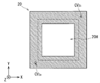
- FIG. 6 is a plan external view of the image sensor layer.
- FIG. 7 is a plan external view of the image sensor holding layer.
- FIG. 8 is a plan external view of the spacer layer.
- FIG. 9 is a plan external view of the actuator layer.
- FIG. 1 is a schematic diagram showing a schematic configuration of a mobile phone equipped with a camera module according to an embodiment.
- FIG. 2 is a schematic cross-sectional view focusing on the first housing according to the embodiment.
- FIG. 3 is
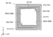
- FIG. 10 is a plan external view of the first and second parallel spring layers.
- FIG. 11 is a plan external view of the imaging lens layer.
- FIG. 12 is a plan external view of the lid layer.
- FIG. 13 is a diagram illustrating a relative arrangement relationship between the actuator layer and the lens unit.
- FIG. 14 is a diagram for explaining the operation of the lens unit due to the deformation of the SMA.
- FIG. 15 is a diagram for explaining the operation of the lens unit due to the deformation of the SMA.
- FIG. 16 is a diagram for explaining the functions of the first and second parallel spring layers.
- FIG. 17 is a diagram for explaining the functions of the first and second parallel spring layers.
- FIG. 18 is a flowchart illustrating an example of the manufacturing process of the camera module.
- FIG. 11 is a plan external view of the imaging lens layer.
- FIG. 12 is a plan external view of the lid layer.
- FIG. 13 is a diagram illustrating a relative arrangement relationship between the actuator layer and the lens
- FIG. 19 is a diagram for explaining a manufacturing process of the camera module.
- FIG. 20 is a schematic cross-sectional view of a camera module according to a modification.
- FIG. 21 is a schematic cross-sectional view of a camera module according to a modification.
- FIG. 22 is a schematic diagram illustrating a configuration example of an actuator layer according to a modification.
- FIG. 23 is a plan external view of an imaging lens layer according to a modification.
- FIG. 24 is a diagram illustrating a relative arrangement relationship between an actuator layer and a lens unit according to a modification.
- FIG. 25 is a diagram for explaining the operation of the actuator layer according to a modified example.
- FIG. 26 is a diagram illustrating a configuration for moving an image sensor according to a modification.
- FIG. 1 is a schematic diagram showing a schematic configuration of a mobile phone 100 equipped with a camera module 500 according to an embodiment of the present invention.
- the mobile phone 100 is configured as a foldable mobile phone, and includes a first casing 200, a second casing 300, and a hinge part 400.
- Each of the first casing 200 and the second casing 300 has a plate-like substantially rectangular parallelepiped shape and serves as a casing for storing various electronic members.
- the first casing 200 includes a camera module 500 and a display
- the second casing 300 includes a control unit that electrically controls the mobile phone 100 and an operation member such as a button.
- the hinge part 400 connects the 1st housing
- the current supply driver 600, the electric resistance detection unit 700, and the contrast detection unit 800 are mounted on the first casing 200.
- the current supply driver 600 controls the supply of current to the shape memory alloy (SMA) film 43 (FIG. 9) of the camera module 500.
- the electric resistance detector 700 detects the electric resistance in the SMA film 43.
- the contrast detection unit 800 detects the contrast of the image signal obtained by the image sensor 11 (FIG. 4) of the camera module 500.
- a focusing control unit 310 is mounted on the second casing 300.
- the focus control unit 310 controls the amount of current supplied to the SMA film 43 via the current supply driver 600 in accordance with the input of signals from the electrical resistance detection unit 700 and the contrast detection unit 800, so that the camera module Auto focus control for adjusting the in-focus state of 500 is performed.
- FIG. 2 is a schematic cross-sectional view focusing on the first casing 200 of the mobile phone 100.
- the camera module 500 is a small imaging device, so-called micro camera unit, having an XY cross-section of about 5 mm square and a thickness (depth in the Z direction) of about several mm. (MCU).
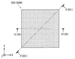
- FIG. 3 is a schematic plan view of the camera module 500.
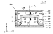
- FIG. 4 is a schematic cross-sectional view of the camera module 500 according to the cut surface indicated by the straight line IV-IV in FIG.
- FIG. 5 is a schematic cross-sectional view of the camera module 500 according to the cut surface indicated by the straight line VV in FIG.
- the camera module 500 includes an imaging element layer 10, an imaging element holding layer 20, a spacer layer 30, an actuator layer 40, a first parallel spring layer 50, an imaging lens layer 60, and a second parallel.
- the eight layers including the spring layer 70 and the lid layer 80 are laminated in this order. Since the two adjacent layers included in the eight layers are joined by a resin such as an epoxy resin, the resin is interposed between the layers.
- each of the layers 10 to 80 has a substantially identical rectangular shape (here, a square having a side of about 5 mm) on the surface in the ⁇ Z direction.
- connecting portions 631a and 631b for connecting the fixed frame body 61 (FIG. 11) and the protruding portion 63 (FIG. 11) are provided.
- the fixed frame body 61 is separated from the lens unit 60U configured to include the optical lens unit 62, the projecting unit 63, and the lens holding units 64a and 64b.
- the lens unit 60 ⁇ / b> U is moved by the actuator layer 40 in the direction along the optical axis PL of the optical lens unit 62 (here, ⁇ Z direction), so that the imaging element 11 and the lens of the imaging element layer 10 are moved.
- the distance from the unit 60U is changed. By changing the distance, autofocus control in which the in-focus state of the camera module 500 is adjusted is realized.
- the camera module 500 is configured in detail as follows.
- An image sensor holding layer 20 for holding the image sensor layer 10 is disposed on the upper surface (+ Z side surface) of the image sensor layer 10, and a spacer is provided on the upper surface (+ Z side surface) of the image sensor layer 20.
- Layer 30 is disposed.
- the spacer layer 30 has a function of securing a space in which the SMA film 43 of the actuator layer 40 undergoes elastic deformation when the lens unit 60U is pushed down in the ⁇ Z direction by the first and second parallel spring layers 50 and 70.
- the actuator layer 40, the first parallel spring layer 50, the imaging lens layer 60, and the second parallel spring layer 70 are stacked in this order on the upper surface of the spacer layer 30, thereby moving the optical lens unit 62.
- Mechanism moving mechanism
- the lens holding portions 64a and 64b of the lens unit 60U are sandwiched from the ⁇ Z direction by the first parallel spring layer 50 and the second parallel spring layer 70, so that the lens unit 60U is placed on the optical axis PL.
- a mechanism parallel link mechanism that is supported so as to be movable in the direction along it is configured. For this reason, the lens unit 60U does not tilt relative to the fixed frame 61 due to the movement in the ⁇ Z direction. Further, a portion (lower end portion) of the protruding portion 63 of the lens unit 60U that is disposed at the ⁇ Z side end portion (lower end portion) contacts the moving member 42 supported by the SMA film 43 of the actuator layer 40. Therefore, a driving device is formed in which the lens unit 60U is moved in the direction along the optical axis PL in accordance with the deformation of the SMA film 43.
- a lid layer 80 made of a transparent material such as glass is disposed on the upper surface of the second parallel spring layer 70.
- the camera module 500 forms a sealed space that includes a space in which the optical lens unit 62 moves.
- the camera module 500 is manufactured, for example, in a clean room or a clean bench, and is maintained so that dust and dust do not enter the sealed space formed by the camera module 500.
- it is possible to suppress the problem that dust or dust adheres to the moving mechanism having a fine gap and the occurrence of air convection in the sealed space.
- variation in load on the drive mechanism is reduced, and the movement accuracy of the optical lens unit 62 is improved.
- the image sensor holding layer 20, the spacer layer 30, and the actuator layer 40 are sequentially formed from the upper surface (+ Z side surface) of the image sensor layer 10 to the upper surface of the actuator layer 40 (+ Z side surface). Holes (through-holes) CVa and CVb that pass through are provided.
- the inner diameters of the minute through holes CVa and CVb are set to about several tens of ⁇ m, for example.
- the through holes CVa and CVb are filled with a conductive material, and the imaging element layer 10 and the SMA film 43 of the actuator layer 40 are electrically connected.
- each functional layer which comprises the camera module 500 is demonstrated.
- 6 to 12 are configuration examples of the imaging element layer 10, the imaging element holding layer 20, the spacer layer 30, the actuator layer 40, the first and second parallel spring layers 50 and 70, the imaging lens layer 60, and the lid layer 80.
- FIG. For each functional layer the ⁇ Z side surface is referred to as one main surface, and the + Z side surface is referred to as the other main surface.
- the imaging element layer 10 is a chip including an imaging element 11 formed by, for example, a COMS sensor or a CCD sensor, a peripheral circuit thereof, and an outer peripheral portion 12 surrounding the imaging element 11.
- wiring for applying a signal to the image sensor 11 and reading a signal from the image sensor 11 is provided on the back surface (the surface on the ⁇ Z side) of the image sensor layer 10.
- Various terminals for connecting are provided.
- the back surface of the imaging element layer 10 is soldered by a reflow method using a solder ball, so that the imaging element layer 10, the current supply driver 600, the electric resistance detection unit 700, the contrast detection unit 800, etc. Are connected so as to be conductive or capable of transmitting and receiving data.
- the imaging element holding layer 20 is a chip that holds the imaging element layer 10 that is formed of a material such as a resin and attached by bonding.
- an opening 20H having a substantially square cross section is provided along the Z direction at a substantially center of the image sensor holding layer 20, and the cross section of the opening 20H goes to the + Z side. The smaller it becomes. 7 indicates the outer edge of the opening 20H on the surface on the ⁇ Z side.
- minute holes (through holes) CV 2a and CV 2b penetrating along the Z direction are provided at two predetermined positions located in the vicinity of two opposing corners of the outer peripheral portion of the image sensor holding layer 20.
- the through holes CV 2a and CV 2b are filled with a conductive material.
- the opening 20H and the through holes CV 2a and CV 2b are formed by, for example, embossing.
- one main surface and the other main surface of the image sensor holding layer 20 are substantially flat, and the one main surface and the other main surface are in a substantially parallel relationship.
- One main surface of the outer peripheral portion of the image sensor holding layer 20 is bonded to the adjacent image sensor layer 10, and the other main surface of the outer peripheral portion is bonded to the adjacent spacer layer 30.
- the spacer layer 30 is a chip that is formed of, for example, a material such as resin and secures a moving space for the lens unit 60U.
- each of the outer edge and the inner edge has an annular shape having a rectangular shape, and has a hollow portion 30 ⁇ / b> H penetrating in the Z direction.
- minute holes (through holes) CV 3a CV penetrating along the Z direction are provided at two predetermined positions located near the two corners facing the spacer layer 30.
- 3b is provided, and the through holes CV 3a and CV 3b are filled with a conductive material.
- the hollow portion 30H and the through holes CV 3a and CV 3b are formed by, for example, embossing.
- one main surface and the other main surface of the spacer layer 30 are substantially flat, and the one main surface and the other main surface are in a substantially parallel relationship. Then, one main surface of the spacer layer 30 is bonded to the adjacent image sensor holding layer 20, and the other main surface is bonded to the adjacent actuator layer 40.
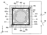
- the actuator layer 40 includes a fixed frame 41, a moving member 42, an SMA film 43, and electrode portions 44a and 44b.
- the fixed frame 41 is a plate-like member formed of a material that is not a conductor, such as silicon.
- the fixed frame body 41 has an annular shape in which the outer edge and the inner edge are each rectangular, and has a hollow portion 41H penetrating in the Z direction.
- the fixed frame 41 includes plate-like portions (plate-like portions) 411 and 413 that extend in the Y direction and face each other, and plates that extend in the X direction and face each other. Shaped portions (plate-like portions) 412 and 414.
- the fixed frame 41 has a shape such that the four plate-like portions 411 to 414 are connected in this order.
- the fixed frame body 41 a portion where the plate-like portion 411 and the plate-like portion 414 are connected protrudes toward the hollow portion 41H, and a portion where the plate-like portion 412 and the plate-like portion 413 are connected is provided. It protrudes toward the hollow portion 41H.
- the fixed frame 41 constitutes the outer peripheral portion of the camera module 500 and functions as a fixing member in the camera module 500.
- the imaging element holding layer 20 and the spacer layer 30 are provided at a total of two locations, that is, a portion where the plate-like portion 411 and the plate-like portion 414 are connected and a portion where the plate-like portion 412 and the plate-like portion 413 are connected.
- minute holes (through holes) CV 4a and CV 4b penetrating along the Z direction are provided, and the through holes CV 4a and CV 4b are filled with a conductive material.
- the through holes CV 4a and CV 4b and the hollow portion 41H are formed by various etchings or the like.
- the conductive material filled in the through hole CV 4a is electrically connected to the conductive material filled in the through holes CV 2a and CV 3a
- the conductive material filled in the through hole CV 4b is the through hole CV. 2b and CV 3b are electrically connected to the conductive material filled.
- the through hole CVa is formed by the through holes CV 2a to CV 4a
- the through hole CVb is formed by the through holes CV 2b to CV 4b .
- the through holes CVa and CVb are filled with a conductive material, whereby through wirings are formed.
- the imaging element layer 10 and the actuator layer 40 are electrically connected by the through wiring.
- the electrical connection between the imaging element layer 10 and the actuator layer 40 can also be realized by providing wiring on the side surface of the camera module 500 using a printing technique or the like.
- the electrode portion 44a is mainly provided on the other main surface of the portion protruding to the hollow portion 41H side in the portion where the plate-like portion 411 and the plate-like portion 414 are connected.
- the electrode portion 44b is mainly provided on the other main surface of the portion protruding toward the hollow portion 41H among the portions where the plate-like portion 412 and the plate-like portion 413 are connected.
- the electrode portion 44a is provided on the other main surface of the through hole CV4a
- the electrode portion 44b is provided on the other main surface of the through hole CV4b.
- the moving member 42 is a plate-like member formed of a material that is not a conductor, such as silicon, for example, like the fixed frame 41.
- the moving member 42 is disposed in the hollow portion 41 ⁇ / b> H so as to be separated from the fixed frame body 41, and is provided to be movable relative to the fixed frame body 41.
- the moving member 42 has a plate-like form, and includes an annular portion 421, relay portions 422a and 422b, and plate-like portions 423a and 423b.
- the annular portion 421 has an annular shape in which the outer edge and the inner edge are each substantially circular, and has a hollow portion 42H that penetrates in the Z direction.
- the relay portion 422a is a plate-like portion that is disposed in the vicinity of a portion where the plate-like portion 411 and the plate-like portion 412 are connected, and has a rectangular outer edge.
- the relay portion 422b is a plate-like portion that is disposed in the vicinity of a portion where the plate-like portion 413 and the plate-like portion 414 are connected, and has a rectangular outer edge like the relay portion 422a.
- the plate-like portion 423a is a portion that connects the annular portion 421 and the relay portion 422a.
- the plate-like portion 423b is a portion that connects the annular portion 421 and the relay portion 422b. As described above, in the moving member 42, the relay portion 422a and the relay portion 422b are connected by the connecting portion configured in the order of the plate-like portion 423a, the annular portion 421, and the plate-like portion 423b.
- the SMA film 43 is made of a shape memory alloy (SMA).
- membrane 43 has the 1st movable part 43a and the 2nd movable part 43b.
- the first movable portion 43a includes a first beam portion 431 and a second beam portion 432, and the second movable portion 43b includes a third beam portion 433 and a fourth beam portion 434. That is, the SMA film 43 has a configuration in which the first beam portion 431, the second beam portion 432, the third beam portion 433, and the fourth beam portion 434 are annularly connected in this order.
- first beam portion 431 is electrically connected to the electrode portion 44a by being fixed on the other main surface of the electrode portion 44a.
- the first beam portion 431 extends in the direction along the Y axis, and the other end portion of the first beam portion 431 is fixed on the other main surface of the relay portion 422a and the second beam portion 432 is provided. It is electrically connected to the other end portion.
- the one end part of the 2nd beam part 432 is electrically connected with respect to the electrode part 44b by being fixed on the other main surface of the electrode part 44b.
- the second beam portion 432 extends in a direction along the X axis, and the other end portion of the second beam portion 432 is fixed on the other main surface of the relay portion 422a, and the first beam portion 431 is provided. It is electrically connected to the other end portion.
- one end of the first movable portion 43a is fixed to a portion in the vicinity of the inner edge of the corner of the fixed frame body 41 via the electrode portion 44a, and the other end of the first movable portion 43a is interposed via the electrode portion 44b.
- the fixed frame body 41 is fixed to a portion in the vicinity of the inner edge of the corner portion, and the substantially central portion of the first movable portion 43a is fixed to the other main surface of the relay portion 422a. That is, the 1st movable part 43a is fixed with respect to the relay part 422a in the location (it is also called a to-be-fixed location) in the middle of the construction path
- the first movable portion 43a is fixed to the electrode portion 44a, the moving member 42, and the electrode portion 44b in this order, so that the first movable portion 43a is a fixed frame on which the electrode portion 44a is provided. It is constructed between a portion in the vicinity of the inner edge of the corner of the body and a portion in the vicinity of the inner edge of the corner of the fixed frame provided with the electrode portion 44b. Thereby, the moving member 42 is supported by the 1st movable part 43a.
- the relay portion 422a as a portion of the moving member 42 to which the first movable portion 43a is fixed, the portion of the electrode portion 44a to which the first movable portion 43a is fixed, and the portion of the electrode portion 44b. It arrange
- a virtual plane (also referred to as a first virtual plane) including a first straight line and a straight line extending in a predetermined direction (here, the ⁇ Z direction) is used as a reference, and the first movable portion 43a
- the to-be-fixed location currently fixed to the relay part 422a is spaced apart from this 1st virtual plane in the direction (it is also called a normal line direction) along the normal line of this 1st virtual plane.
- position of the 1st movable part 43a is controlled by the construction form via the moving member 42 in the state constructed in L shape seeing from the other main surface side.
- the length of the construction path of the first movable part 43a between the electrode part 44a and the electrode part 44b is the first movable part of the electrode part 44a.
- the distance between the portion where the portion 43a is fixed and the portion of the electrode portion 44b where the first movable portion 43a is fixed is set to be relatively longer.
- the relative positional relationship between the electrode portion 44a as the first reference portion and the electrode portion 44b as the second reference portion is fixed.
- one end portion of the third beam portion 433 is fixed on the other main surface of the electrode portion 44b, thereby being electrically connected to the electrode portion 44b.
- the third beam portion 433 extends in a direction along the Y axis, and the other end portion of the third beam portion 433 is fixed on the other main surface of the relay portion 422b, and the fourth beam portion 434 is provided. It is electrically connected to the other end portion.
- one end of the fourth beam portion 434 is electrically connected to the electrode portion 44a by being fixed on the other main surface of the electrode portion 44a.
- the fourth beam portion 434 extends in the direction along the X axis, and the other end portion of the fourth beam portion 434 is fixed on the other main surface of the relay portion 422b, and the third beam portion 433 is provided. It is electrically connected to the other end portion.
- one end of the second movable portion 43b is fixed to a portion near the inner edge of the corner portion of the fixed frame 41 via the electrode portion 44a, and the other end of the second movable portion 43b is interposed via the electrode portion 44b.
- the fixed frame body 41 is fixed to a portion near the inner edge of the corner portion, and the substantially central portion of the second movable portion 43b is fixed to the other main surface of the relay portion 422b. That is, the 2nd movable part 43b is fixed with respect to the relay part 422b in the location (it is also called a to-be-fixed location) in the middle of the construction path
- the second movable portion 43b is fixed to the electrode portion 44a, the moving member 42, and the electrode portion 44b in this order, so that the second movable portion 43b is a fixed frame provided with the electrode portion 44a. It is constructed between a portion in the vicinity of the inner edge of the corner of the body and a portion in the vicinity of the inner edge of the corner of the fixed frame provided with the electrode portion 44b. Thereby, the moving member 42 is supported by the 2nd movable part 43b.
- the relay part 422b as the part to which the second movable part 43b of the moving member 42 is fixed is the same as the part of the electrode part 44a to which the second movable part 43b is fixed and the electrode part 44b. It arrange
- a virtual plane (also referred to as a second virtual plane) including the second straight line and a straight line extending in a predetermined direction (here, the ⁇ Z direction) is used as a reference, and the second movable portion 43b
- the to-be-fixed location currently fixed to the relay part 422b is spaced apart from this 2nd virtual plane in the direction (it is also called a normal line direction) along the normal line of this 2nd virtual plane.
- position of the 2nd movable part 43b is controlled by the installation form via the moving member 42 in the state installed in L shape seeing from the other main surface side.
- the length of the construction path of the second movable part 43b between the electrode part 44a and the electrode part 44b is the second movable part of the electrode part 44a.
- the distance between the portion where the portion 43b is fixed and the portion where the second movable portion 43b of the electrode portion 44b is fixed is set to be relatively longer.
- a voltage is applied between the electrode portion 44a and the electrode portion 44b by applying a voltage from the outside to the through wirings of the through holes CVa and CVb.
- a current flows through the film 43.
- the first and second movable portions 43a and 43b generate heat due to Joule heat, and the first and second movable portions 43a and 43b are deformed according to the generated heat.
- the moving member 42 moves relative to the fixed frame 41 provided with the electrode portions 44a and 44b. The movement of the moving member 42 due to the deformation of the first and second movable parts 43a and 43b will be further described later.
- one main surface and the other main surface of the fixed frame 41 are substantially flat, and the one main surface and the other main surface are in a substantially parallel relationship. Then, one main surface of the fixed frame body 41 is bonded to the adjacent spacer layer 30, and the other main surface is bonded to the fixed frame body 51 (FIG. 10) of the adjacent first parallel spring layer 50. In addition, between the actuator layer 40 and the first parallel spring layer 50, a resin or the like used for bonding is interposed, so that the electrode portions 44a and 44b and the SMA film 43 and the first parallel spring layer 50 are interposed. It is configured so as not to cause a short circuit.
- the first parallel spring layer 50 of the other main surface of the actuator layer 40 is joined. It is preferable that an insulating film is formed on the portion.
- the first parallel spring layer 50 is an elastic member having a fixed frame body 51 and an elastic portion 52, and is a layer (elastic layer) forming a spring mechanism.
- a material of the first parallel spring layer 50 for example, a metal material such as stainless steel, phosphor bronze, or the like is employed.
- the fixed frame 51 constitutes the outer peripheral portion of the first parallel spring layer 50.
- the elastic portion 52 includes connection portions 51a and 51b with the fixed frame 51 and joint portions 52a and 52b with the lens unit 60U, and the connection portions 51a and 51b and the joint portions 52a and 52b are plate-like members 50EB.
- the first parallel spring layer 50 is bonded to the lens holding portions 64a and 64b of the lens unit 60U at the bonding portions 52a and 52b.
- the projecting portion 63 of the lens unit 60 ⁇ / b> U passes through the hollow portion formed inside the elastic portion 52 without contacting the first parallel spring layer 50, and other than the annular portion 421 of the actuator layer 40. Abuts against the main surface.
- the lens unit 60U As the lens unit 60U is moved in the + Z direction with respect to the fixed frame 51, the positions of the connecting portions 51a and 51b and the joint portions 52a and 52b in the Z direction are shifted, and the plate-like member 50EB is bent and deformed (deflection). Deformation) and bends. That is, the first parallel spring layer 50 can be elastically deformed in the optical axis direction ( ⁇ Z direction) of the optical lens portion 62 by elastic deformation of the plate-like member 50EB, and functions as a spring mechanism.
- one main surface and the other main surface of the fixed frame 51 are each configured to be substantially flat, and the one main surface and the other main surface are configured to be substantially parallel. Then, one main surface of the fixed frame 51 is joined to the fixed frame 41 of the adjacent actuator layer 40, and the fixed frame 61 of the imaging lens layer 60 where the other main surface of the fixed frame 51 is adjacent (FIG. 11). It is joined with one main surface.
- the second parallel spring layer 70 has a fixed frame body 51, an elastic portion 52, connection portions 51 a and 51 b, joint portions 52 a and 52 b, as compared with the first parallel spring layer 50.
- the plate-like member 50EB is changed to a fixed frame 71, an elastic portion 72, connection portions 71a and 71b, joint portions 72a and 72b, and a plate-like member 70EB each having the same configuration.
- the second parallel spring layer 70 is also a layer (elastic layer) forming a spring mechanism.
- one main surface of the fixed frame 71 is joined to the other main surface of the fixed frame 61 (FIG. 11) of the adjacent imaging lens layer 60, and the other main surface of the fixed frame 71.
- the surface is bonded to one main surface of the outer peripheral portion of the adjacent lid layer 80.
- the imaging lens layer 60 includes a fixed frame body 61 and a lens unit 60U.
- Examples of the material constituting the imaging lens layer 60 include phenolic resins and acrylic resins.
- the fixed frame 61 constitutes the outer peripheral portion of the imaging lens layer 60, and has a thickness corresponding to the thickness of the lens unit 60U in the Z direction.
- the fixed frame 61 has an annular shape in which the outer edge and the inner edge are each rectangular, and has a hollow portion 60H penetrating in the Z direction.
- the one main surface and the other main surface of the fixed frame 61 are configured to be substantially flat, and the one main surface and the other main surface are configured to be substantially parallel to each other. Then, one main surface of the fixed frame body 61 is joined to the other main surface of the fixed frame body 51 of the adjacent first parallel spring layer 50, and the other main surface of the fixed frame body 61 is adjacent to the second parallel spring layer 70. It is joined to one main surface of the fixed frame 71.
- the lens unit 60U is disposed in the hollow portion 60H and includes an optical lens portion 62, a projecting portion 63, and lens holding portions 64a and 64b.
- the optical lens unit 62 is an optical system that guides light from a subject to the image sensor 11 and has positive lens power.
- the projecting portion 63 is provided on the side surface around the optical lens portion 62 and has a substantially cylindrical shape with the optical axis of the optical lens portion 62 as the central axis.
- One main surface of the projecting portion 63 abuts on the annular portion 421 of the moving member 42.
- the lens unit 60U which is a moving object, comes into contact with the moving member 42 moved by the first and second movable parts 43a and 43b by the protruding part 63.
- One main surface of the protruding portion 63 may be fixed to the annular portion 421 with an adhesive or the like.
- the lens holding portion 64 a is a portion protruding along the diagonal line of the fixed frame 61 from the side surface of the protruding portion 63.
- the front end portion of the lens holding portion 64a has a shape protruding in each of the + Z direction and the ⁇ Z direction, and one main surface and the other main surface of the front end portion are configured to be substantially flat, and the one main surface and the other The main surface is configured substantially parallel. Then, one main surface of the tip portion of the lens holding portion 64a is bonded to the bonding portion 52a of the first parallel spring layer 50, and the other main surface of the tip portion of the lens holding portion 64a is the second parallel spring layer 70. It joins with respect to the joining part 72a.
- the lens holding portion 64b is a portion that protrudes along the diagonal line of the fixed frame 61 from the side surface of the protruding portion 63 that is substantially opposite to the surface on which the lens holding portion 64a is protruded.
- the tip end portion of the lens holding portion 64b has a shape protruding in each of the + Z direction and the ⁇ Z direction, and one main surface and the other main surface of the tip portion are configured to be substantially flat.
- the one main surface and the other main surface are configured to be substantially parallel.
- one main surface of the tip portion of the lens holding portion 64b is bonded to the bonding portion 52b of the first parallel spring layer 50, and the other main surface of the tip portion of the lens holding portion 64b is the second parallel spring layer 70. Are joined to the joint 72b.
- the connecting portions 631a and 631b drawn in broken lines are femtoseconds.
- the fixed frame 61 and the lens unit 60U are separated by cutting with a laser or the like.
- the lid layer 80 is a plate-like member having a board surface whose outer edge in the XY section is substantially square and substantially parallel to the XY plane.
- the lid layer 80 is made of a transparent material such as a resin, plays a role of introducing light from the subject into the camera module 500, and seals the inside of the camera module 500 so that the inside of the camera module 500 is sealed. It plays a role to prevent dust and dust from entering.
- one main surface of the outer peripheral portion of the lid layer 80 is joined to the fixed frame 71 of the second parallel spring layer 70.
- FIG. 13 is a schematic diagram showing a relative arrangement relationship between the actuator layer 40 and the lens unit 60U.
- FIG. 13 shows a configuration focusing on the actuator layer 40 and only the lens unit 60U of the imaging lens layer 60, and other layers such as the first and second parallel spring layers 50 and 70 are as follows. The illustration is omitted.
- the actuator layer 40 has a pair of movable parts (specifically, first and second movable parts 43 a and 43 b) across the optical axis of the optical lens part 62.
- first and second movable parts 43 a and 43 b movable parts across the optical axis of the optical lens part 62.
- the first beam portion 431 and the second beam portion 432 are electrically connected in series
- the second movable portion 43b the third beam portion 433 and the fourth beam portion 434 are connected.
- the first and second movable parts 43a and 43b are electrically connected in parallel between the electrode part 44a and the electrode part 44b.
- a power source PW is connected between the electrode portions 44a and 44b from the outside, and the electrode portion 44a and the electrode portion 44b are connected according to the opening / closing of the switch SW in the current supply driver 600. A voltage is applied between them.
- each movable part 43a, 43b is heated by generation
- transforms so that a center part may be pushed down by being cooled (here air cooling) from the state heated by completion
- the deformation of each of the movable parts 43a and 43b and the movement of the lens unit 60U will be specifically described below.
- FIG. 14 and 15 are schematic views for explaining the operation of the lens unit 60U due to the deformation of the SMA film 43.
- FIG. 14 and 15 show a configuration in which attention is paid to the actuator layer 40, the first parallel spring layer 50, and the lens unit 60U.
- the protruding portion 63 of the lens unit 60U comes into contact with the moving member 42 supported by the first and second movable portions 43a and 43b.
- the plate-like shape of the first and second parallel spring layers 50 and 70 is obtained. Due to the elastic force with which the members 50EB and 70EB become flat, the lens unit 60U is pushed down in the ⁇ Z direction. At this time, when the moving member 42 is pushed down in the ⁇ Z direction by the projecting portion 63, the substantially central portions of the first and second movable portions 43a and 43b are pushed down in the ⁇ Z direction by the relay portions 422a and 422b. The first and second movable parts 43a and 43b bend.
- the first and second parallel spring layers 50 and 70 are directed to the moving member 42 in a predetermined direction (here, the resistance against the tension by the first and second movable portions 43a and 43b via the lens unit 60U. Apply force in the -Z direction). At this time, the actuator layer 40 is precharged by the first and second parallel spring layers 50 and 70.
- first and second movable parts 43a and 43b are shifted from the non-driven state to a state where the first and second movable parts 43a and 43b are heated by energization (drive state), as shown in FIG. 43b is deformed from a bent state to a flattened direction. That is, the first and second movable parts 43a and 43b are deformed so as to reduce the amount of bending.
- a force that pushes up the lens unit 60U by the first and second movable portions 43a and 43b against the elastic force of the plate-like members 50EB and 70EB is applied, and the lens unit 60U moves in the + Z direction.
- the position of the lens unit 60U is the original position shown in FIG. Return to position.
- the optical lens 62 is in the optical axis in the driving state. Accordingly, it is possible to move the lens unit 60U in the + Z direction within a range up to the distance ⁇ 0 with reference to the initial position.
- the first movable portion 43 a is not installed in a substantially linear shape, but sequentially in the direction along the inner edge of the plate-like portion 411 and the inner edge of the plate-like portion 412 of the fixed frame 41.
- the second movable portion 43b is not installed in a substantially straight line, but in a direction along the inner edge of the plate-like portion 413 and the inner edge of the plate-like portion 414 of the fixed frame body 41. It is erected in an L shape by being erected sequentially.
- the installation path of the first and second movable parts 43a and 43b becomes longer than the case where the movable part is simply installed in a straight line. .
- an increase in the distance ⁇ 0 that can push down the substantially central part of the first and second movable parts 43a, 43b in the ⁇ Z direction while elastically deforming the first and second movable parts 43a, 43b is achieved. It is done. As a result, it is possible to increase the distance by which the lens unit 60U that is the moving object can be displaced along the Z axis.
- the rigidity of the structure (here, the fixed frame 41 and the like) to which both ends of the first and second movable parts 43a and 43b are fixed can be reduced.
- the camera module 500 can be reduced in size and weight.
- FIG. 16 and 17 are schematic views for explaining the functions of the first and second parallel spring layers 50 and 70.
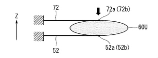
- FIG. 16 and 17 are schematic views of the lens unit 60U and the elastic portions 52 and 72 as viewed from the side. As shown in FIGS. 16 and 17, the elastic portions 52 and 72 are joined to the lens unit 60U at the joint portions 52a, 52b, 72a and 72b, respectively, thereby sandwiching the lens unit 60U. Further, FIG. 16 shows a state where the elastic portions 52 and 72 are hardly deformed (initial state), and FIG. 17 shows a state where the elastic portions 52 and 72 are deformed to some extent (deformed state). Yes.
- the elastic portions 52 and 72 have the same configuration, and are similarly fixed to the fixed frame bodies 51 and 71 at two locations (connection portions 51a and 51b and connection portions 71a and 71b). Is done. Similarly, the elastic portions 52 and 72 are joined to the lens unit 60U at two locations (joining portions 52a and 52b and joining portions 72a and 72b).
- the elastic parts 52, 72 perform substantially the same deformation.
- the optical lens unit 62 included in the lens unit 60U moves in the vertical direction (here, the direction along the Z axis) without the optical axis being inclined. That is, the distance between the optical lens unit 62 and the image sensor 11 is changed without shifting the direction of the optical axis of the optical lens unit 62. As a result, the distance between the image sensor 11 and the optical lens unit 62 is changed, and autofocus control for performing focus adjustment is executed.
- the autofocus control in the camera module 500 is realized by the current supply driver 600, the electric resistance detection unit 700, the contrast detection unit 800, and the focus control unit 310 shown in FIG.
- the electrical resistance detection unit 700 detects the electrical resistance of the SMA film 43 and outputs a signal indicating the electrical resistance to the focusing control unit 310.
- the focusing control unit 310 detects deformation of the SMA film 43 (specifically, displacement of the central portions of the first and second movable parts 43a and 43b) based on the electrical resistance of the SMA film 43. That is, the electrical resistance detection unit 700 and the focus control unit 310 detect the electrical resistances related to the first and second movable parts 43a and 43b, so that the displacements related to the first and second movable parts 43a and 43b are changed. Be recognized. And here, the displacement of the center part of the 1st and 2nd movable parts 43a and 43b turns into the displacement of the lens unit 60U.
- the relationship between the shape and the electrical resistance in the SMA film 43 (specifically, the first and second movable parts 43a, 43b) is unambiguous. Is determined and used. With such a configuration, the displacement relating to the first and second movable parts 43a and 43b is easily detected.
- the focus control unit 310 controls the supply of current to the SMA film 43 via the current supply driver 600 while detecting the displacement of the central portions of the first and second movable units 43a and 43b.
- the deformation amount of the first and second movable parts 43a and 43b that is, the displacement of the central part of the first and second movable parts 43a and 43b is controlled.
- the moving member 42 is pulled up by the central portion, and the lens unit 60U is pushed up by the moving member 42.
- the lens unit 60U is moved in the + Z direction, the separation distance between the optical lens unit 62 and the image sensor 11 is changed, and the focus position is changed.
- the contrast detection unit 800 detects the contrast of the image signal obtained by the image sensor 11. For example, a numerical value obtained by accumulating differences in gradation values between adjacent pixels for the entire image is detected as an evaluation value indicating contrast. A signal indicating the evaluation value indicating the contrast is output to the focus control unit 310.
- the separation distance between the lens unit 60U and the image sensor 11 is sequentially set to a preset multi-step separation distance under the control of the focusing control unit 310, and each separation distance is set.
- An image signal is acquired by the imaging device 11 in a state where the lens unit 60U and the imaging device 11 are set to the distance.
- the extension position of the lens unit 60U in the + Z direction is set to a preset multi-stage position, and an image signal is output by the imaging device 11 at the time when the lens unit 60U is disposed at each extension position.
- the focus control unit 310 controls the supply of current to the SMA film 43 via the current supply driver 600 while monitoring the electrical resistance of the SMA film 43 detected by the electrical resistance detection unit 700.
- the feeding position of the lens unit 60U is changed.
- the focus control unit 310 detects a feeding position where the evaluation value indicating the contrast is maximum based on the evaluation value indicating the contrast detected for each feeding position by the contrast detection unit 800.
- the state in which the lens unit 60U is disposed at the extended position where the evaluation value indicating the contrast is maximum corresponds to the state in which the subject is in focus.
- the lens unit 60U is moved to the extended position where the evaluation value indicating the contrast is maximized, thereby achieving focusing on the subject in the camera module 500. That is, autofocus control is realized.
- FIG. 18 is a flowchart illustrating the procedure of the manufacturing process of the camera module 500.
- Step S1 preparation of a plurality of sheets
- Step S2 joining of a plurality of sheets
- Step S3 joining of a plurality of sheets
- Step S3 dicing
- the image sensor layer sheet U10 is a sheet in which a large number of chips corresponding to the image sensor layer 10 are formed in a matrix-like predetermined arrangement.
- the imaging element layer sheet U10 is manufactured, for example, by forming the imaging element 11 and various circuits on a disk-shaped silicon substrate.
- the imaging element holding layer sheet U20 is a sheet in which a large number of chips corresponding to the imaging element holding layer 20 are formed in a matrix-like predetermined arrangement.
- the image pickup element holding layer sheet U20 for example, with respect to the material disc-like wafer which is formed by a resin or the like, the opening 20H and the through hole CV 2a by embossing or the like, CV 2b is formed, the through hole CV 2a , CV 2b is manufactured by being filled with a conductive material by metal plating or the like.
- the spacer layer sheet U30 is a sheet in which a large number of chips corresponding to the spacer layer 30 are formed in a matrix-like predetermined arrangement.
- a hollow portion 30H and through holes CV 3a and CV 3b are formed by stamping or the like on a disk-shaped wafer formed of a material such as a resin, and the through holes CV 3a ,
- the CV 3b is manufactured by being filled with a conductive material by metal plating or the like.
- the actuator layer sheet U40 is a sheet in which a number of chips corresponding to the actuator layer 40 are formed in a matrix-like predetermined arrangement.
- the actuator layer sheet U40 is manufactured, for example, by sequentially performing the following steps (I) to (VII).
- a silicon substrate is prepared.
- Through holes CV4a and CV4b are formed in the silicon substrate by etching or the like using a photolithography technique.
- the through holes CV 4a and CV 4b may be formed by etching such as DRIE (Deep Reactive Ion Etching).
- the through holes CV 4a and CV 4b are filled with a conductive material by metal plating or the like.
- the electrode portions 44a and 44b are formed at positions covering the through holes CV 4a and CV 4b of the silicon substrate by coating or vapor deposition using a printing technique.
- a thin film of shape memory alloy is formed on the silicon substrate by sputtering or the like.
- the shape memory alloy thin film is subjected to a heat treatment (memory heat treatment) for memorizing the shape so that it shrinks during high temperature heating.
- the thin film of shape memory alloy memorizes a planar shape.
- the SMA film 43 having the shapes of the first and second movable portions 43a and 43b is formed by etching the shape memory alloy thin film using a photolithography technique or the like.
- the hollow portions 41H and 42H are formed by subjecting the silicon substrate to selective etching using hydrofluoric acid, which is a mixed liquid of hydrofluoric acid and nitric acid.
- a lattice-shaped portion constituting the fixed frame body 41 and a moving member 42 disposed in each lattice-shaped hollow portion 41H are formed. Accordingly, the first movable portion 43a is installed between the electrode portion 44a and the electrode portion 44b so as to pass through the relay portion 422a, and the second movable portion 43b is connected to the electrode portion so as to pass through the relay portion 422b. It will be in the state constructed between 44a and the electrode part 44b.
- the first parallel spring layer sheet U50 is a sheet in which a large number of chips corresponding to the first parallel spring layer 50 are formed in a matrix-like predetermined arrangement.
- the first parallel spring layer sheet U50 is formed by applying a resist in the shape of a parallel spring on a metal material by photolithography on a disk-shaped wafer formed of a metal material such as stainless steel or a material such as phosphor bronze.
- a pattern of parallel springs is formed by performing wet etching by immersing in an iron chloride-based etching solution.
- the imaging lens layer sheet U60 is a sheet in which a large number of chips corresponding to the imaging lens layer 60 are formed in a matrix-like predetermined arrangement. However, in the imaging lens layer sheet U60, in each chip, the fixed frame 61 and the protruding portion 63 are connected by the connecting portions 631a and 631b.
- the imaging lens layer sheet U60 is manufactured, for example, by resin molding.
- the second parallel spring layer sheet U70 is a sheet in which a large number of chips corresponding to the second parallel spring layer 70 are formed in a matrix-like predetermined arrangement.
- the second parallel spring layer sheet U70 is manufactured in the same process as the first parallel spring layer sheet U50.
- the lid layer sheet U80 is a sheet in which a large number of chips corresponding to the lid layer 80 are formed in a matrix-like predetermined arrangement.
- the lid layer sheet U80 is manufactured, for example, by resin molding.
- the cover layer sheet U80 may be flat glass.
- the eight sheets U10 to U80 prepared in the process A are provided with marks (alignment marks) for alignment in the sheet joining process at substantially the same positions.
- alignment marks include marks such as crosses and the like, and are preferably provided at two or more positions in the vicinity of the outer peripheral portion of the upper surface of each of the sheets U10 to U80.
- alignment is performed with the sheet shape so that the chips of the second parallel spring layer sheet U70 and the imaging lens layer sheet U60 are arranged and stacked immediately above each other.
- the second parallel spring layer sheet U70 and the imaging lens layer sheet U60 are set in a known aligner device, and alignment is performed using a previously formed alignment mark.
- a so-called epoxy resin adhesive or ultraviolet curable adhesive is applied in advance to the surface (joint surface) to which the second parallel spring layer sheet U70 and the imaging lens layer sheet U60 are joined, Both sheets U60 and U70 are joined.
- a method may be used in which the joining surfaces are activated by irradiating the joining surfaces with O2 plasma and both sheets U60 and U70 are directly joined.
- each lens holding portion 64a of the imaging lens layer sheet U60 is bonded to each bonding portion 72a of the second parallel spring layer sheet U70, and each lens holding portion 64b of the imaging lens layer sheet U60 is second parallel. It joins with respect to each joining part 72b of the spring layer sheet
- the connecting portions 631a and 631b that connect the fixed frame body 61 and the projecting portion 63 are cut, thereby fixing the fixed frame.
- the body 61 and the projecting portion 63 are separated.
- an imaging element layer sheet U10, an imaging element holding layer sheet U20, a spacer layer sheet U30, an actuator layer sheet U40, a first layer are formed on the upper and lower surfaces of a laminate formed by laminating two sheets U60 and U70.
- the parallel spring layer sheet U50 and the lid layer sheet U80 are aligned (aligned) while maintaining the sheet shape.
- the chips of the eight sheets U10 to U80 are arranged and stacked immediately above each other.
- the first parallel spring layer sheet U50 is joined on the imaging lens layer sheet U60 by the same alignment and joining method as described above, and then the actuator layer sheet U40 is placed on the first parallel spring layer sheet U50.
- the spacer layer sheet U30 is bonded onto the actuator layer sheet U40.
- the imaging element holding layer sheet U20 is joined on the spacer layer sheet U30, and then the imaging element layer sheet U10 is joined on the imaging element holding layer sheet U20.
- the lid layer sheet U80 is bonded onto the second parallel spring layer sheet U70 by the same alignment and bonding method as described above.
- each lens holding portion 64a of the imaging lens layer sheet U60 is connected to each bonding portion 52a of the first parallel spring layer sheet U50.
- the lens holding portions 64b of the imaging lens layer sheet U60 are joined to the joint portions 52b of the first parallel spring layer sheet U50.
- the actuator layer sheet U40 is bonded onto the first parallel spring layer sheet U50, so that each protruding portion 63 of the imaging lens layer sheet U60 comes into contact with the annular portion 421 of the moving member 42.
- the three sheets U20 to U40 are joined, so that the conductive materials filled in the through holes CV 2a to CV 4a are electrically connected to each other, thereby forming the through holes CVa.
- a through wiring is formed.
- the conductive material filled in the through holes CV 2b to CV 4b is electrically connected to each other, thereby forming a through wiring formed by the through hole CVb.
- the first movable portion 43a is not provided in a straight line in the actuator layer 40, and the electrode portion is interposed via the relay portion 422a. It is installed between 44a and the electrode part 44b.
- the second movable part 43b is installed between the electrode part 44a and the electrode part 44b via the relay part 422b without being installed in a straight line. For this reason, it sets so that the length of the construction path
- each movable part 43a, 43b may be constructed in the hollow portion of the fixed frame body through two or more moving members sequentially.
- FIG. 20 is a schematic cross-sectional view of the camera module 500A according to the modified example, taken along a cut surface indicated by a straight line XX-XX in FIG.
- FIG. 21 is a schematic cross-sectional view of the camera module 500A taken along the cut surface indicated by the straight line XXI-XXI in FIG.
- the image sensor holding layer 20A, the spacer layer 30, the actuator layer 40, and the image pickup lens layer 60 constituting the camera module 500 according to the embodiment
- the image sensor holding layer 20A, the spacer layer 30A A description will be given assuming that the mobile phone 100A having the first housing 200A on which the camera module 500A is mounted is configured by employing the actuator layer 40A and the imaging lens layer 60A.
- the same parts as those in the cellular phone 100 and the camera module 500 according to the above embodiment are denoted by the same reference numerals and the description thereof is omitted. The different parts will be described.
- the camera module 500A includes an image sensor layer 10, an image sensor holding layer 20A, a spacer layer 30A, an actuator layer 40A, a first parallel spring layer 50, an image pickup lens layer 60A, and a second parallel.
- the eight layers including the spring layer 70 and the lid layer 80 are laminated in this order.
- the imaging lens layer 60A during the manufacturing of the camera module 500A, for example, the connecting portions 631aA and 631bA that connect the fixed frame 61 (FIG. 23) and the projecting portion 63A (FIG. 23) are cut, and the optical The lens unit 60UA configured to include the lens portion 62A, the projecting portion 63A, and the lens holding portions 64aA and 64bA is separated from the fixed frame body 61.
- the actuator layer 40A, the first parallel spring layer 50, the imaging lens layer 60A, and the second parallel spring layer 70 are laminated in this order on the upper surface of the spacer layer 30A, thereby moving the optical lens portion 62A.
- the mechanism (movement mechanism) is configured.
- the lens holding portions 64aA and 64bA of the lens unit 60UA are sandwiched from the ⁇ Z direction by the first parallel spring layer 50 and the second parallel spring layer 70, and thus in the direction along the optical axis PL.
- the mechanism (parallel link mechanism) supported so that a movement is possible is comprised. For this reason, the lens unit 60UA does not tilt relative to the fixed frame 61 due to the movement in the ⁇ Z direction.
- a portion (lower end portion) of the protruding portion 63A of the lens unit 60UA disposed at the end on the ⁇ Z side is in contact with the moving member 42A supported by the SMA film 43A of the actuator layer 40A. For this reason, a driving device is formed in which the lens unit 60UA is moved in the direction along the optical axis PL in accordance with the deformation of the SMA film 43A.
- the image sensor holding layer 20 ⁇ / b> A according to the modification is obtained by changing the positions of the through holes CV 2 a and CV 2 b as compared with the image sensor holding layer 20 according to the embodiment.
- the spacer layer 30A according to the modification is obtained by changing the positions of the through holes CV 3a and CV 3b as compared with the spacer layer 30 according to the embodiment.
- the arrangement positions of the through holes CV 2a , CV 2b , CV 3a , CV 3b will be described later.
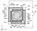
- the actuator layer 40A according to the modification includes a fixed frame 41A, two moving members 42A and 45, an SMA film 43A, electrode portions 441a, 441b, 444a, and 444b, and a wiring portion 442a, 442b, 443a, 445a, 445b, 446b.
- the fixed frame body 41A is a plate-like member formed of a material that is not a conductor, such as silicon, for example, similarly to the fixed frame body 41 according to the one embodiment.
- the fixed frame body 41A has an annular shape whose outer edge and inner edge are each rectangular, and has a hollow portion 41HA penetrating in the Z direction.
- the fixed frame body 41A includes plate-like portions (plate-like portions) 411A and 413A that extend in the Y direction and face each other, and plates that extend in the X direction and face each other.
- Shaped portions (plate-like portions) 412A and 414A The fixed frame 41A has a shape such that the four plate-like portions 411A to 414A are connected in this order.
- the fixed frame body 41A constitutes the outer peripheral portion of the camera module 500A and functions as a fixing member in the camera module 500A.
- imaging is performed at a total of two locations including a portion where the plate-like portion 411A and the plate-like portion 412A are connected and a portion where the plate-like portion 413A and the plate-like portion 414A are connected.
- a minute hole is provided from one main surface along the Z direction, and the through hole is filled with a conductive material.
- the through hole and the hollow portion 41HA are formed by various etchings or the like.
- the conductive material filled in the through hole CV 4a is electrically connected to the conductive material filled in the through holes CV 2a and CV 3a to form a through wiring, and is filled in the through hole CV 4b.
- the conductive material is electrically connected to the conductive material filled in the through holes CV 2b and CV 3b to form a through wiring.
- the wiring part 443a is provided on the other main surface of the part where the plate-like part 411A and the plate-like part 412A are connected, and the through-wirings related to the through holes CV 2a and CV 3a are provided directly below the wiring part 443a. Is formed.
- a wiring portion 446b is provided on the other main surface of the portion where the plate-like portion 413A and the plate-like portion 414A are connected, and through-hole wirings related to the through holes CV 2b and CV 3b are formed immediately below the wiring portion 446b.
- the electrode portion 441a is provided on the other main surface in the vicinity of the end connected to the plate-like portion 414A of the plate-like portion 411A.
- the electrode portion 441a is provided on the other main surface of the portion of the fixed frame 41A that protrudes toward the hollow portion 41HA.
- the electrode portion 441b is provided on the other main surface in the vicinity of the end connected to the plate-like portion 413A of the plate-like portion 412A.
- the electrode portion 441b is provided on the other main surface of the portion of the fixed frame 41A that protrudes toward the hollow portion 41HA.
- the electrode portion 444a is provided on the other main surface in the vicinity of the end connected to the plate-like portion 411A of the plate-like portion 414A.
- the electrode portion 444a is provided on the other main surface of the portion of the fixed frame body 41A that protrudes toward the hollow portion 41HA. Furthermore, the electrode portion 444b is provided on the other main surface in the vicinity of the end connected to the plate-like portion 412A of the plate-like portion 413A. The electrode portion 444b is provided on the other main surface of the portion protruding to the hollow portion 41HA side of the fixed frame body 41A.
- the wiring portion 442a extends along the extending direction of the plate-like portion 411A on the other main surface of the plate-like portion 411A, and electrically connects the electrode portion 441a and the wiring portion 443a.
- the wiring part 442b extends along the extending direction of the plate-like part 412A on the other main surface of the plate-like part 412A, and electrically connects the electrode part 441b and the wiring part 443a.
- the wiring portion 445a extends along the extending direction of the plate-like portion 414A on the other main surface of the plate-like portion 414A, and electrically connects the electrode portion 444a and the wiring portion 446b.
- the wiring portion 445b extends along the extending direction of the plate-like portion 413A on the other main surface of the plate-like portion 413A, and electrically connects the electrode portion 444b and the wiring portion 446b.
- the moving member 45 is a plate-like member formed of a material that is not a conductor, such as silicon, for example, like the fixed frame body 41A.
- the moving member 45 is disposed in the hollow portion 41HA so as to be separated from the fixed frame body 41A, and is provided so as to be movable relative to the fixed frame body 41A.
- the moving member 45 has a plate-like form and includes relay portions 451a and 451b and L-shaped plate-like connecting portions 452a and 452b.
- the relay portion 451a is a plate-like portion that is disposed in the vicinity of a portion where the plate-like portion 411A and the plate-like portion 412A are connected, and has a rectangular outer edge.
- the relay portion 451b is a plate-like portion that is disposed in the vicinity of the portion where the plate-like portion 413A and the plate-like portion 414A are connected, and has a rectangular outer edge, like the relay portion 451a.
- the L-shaped plate-like connecting portion 452a extends from the relay portion 451a to the relay portion 451b via the space near the inner edge of the connecting portion between the plate-like portion 411A and the plate-like portion 414A.
- An L-shaped plate-like connecting part 452a connects the relay part 451a and the relay part 451b. Further, the L-shaped plate-like connecting portion 452b extends from the relay portion 451a to the relay portion 451b via a space near the inner edge of the connecting portion between the plate-like portion 412A and the plate-like portion 413A. The L-shaped plate-like connecting portion 452b connects the relay portion 451a and the relay portion 451b. With such a configuration, the moving member 45 forms the hollow portion 45H.
- the moving member 42A is a plate-like member formed of a non-conductive material such as silicon, for example, like the fixed frame body 41A and the moving member 45.
- the moving member 42 ⁇ / b> A is disposed in the hollow portion 45 ⁇ / b> H so as to be separated from the moving member 45, and is provided to be movable relative to the fixed frame body 41 ⁇ / b> A and the moving member 45.
- the moving member 42A has a plate-like form and includes an annular portion 421A, relay portions 422aA and 422bA, and plate-like portions 423aA and 423bA.
- the annular portion 421A has an annular shape in which the outer edge and the inner edge are substantially circular, respectively, and has a hollow portion 42HA penetrating in the Z direction.
- the relay portion 422aA is a plate-like portion that is disposed in the vicinity of the inner edge of the corner portion where the L-shaped plate-like connecting portion 452a is bent and whose outer edge is rectangular.
- the relay portion 422bA is a plate-like portion that is disposed in the vicinity of the inner edge of the corner where the L-shaped plate-like connecting portion 452b bends and the outer edge is rectangular.
- the plate-like portion 423aA is a portion that connects the annular portion 421A and the relay portion 422aA.
- the plate-like portion 423bA is a portion that connects the annular portion 421A and the relay portion 422bA.
- the relay portion 422aA and the relay portion 422bA are connected by the connecting portion configured in the order of the plate-like portion 423aA, the annular portion 421A, and the plate-like portion 423bA.
- the SMA film 43A is configured using a shape memory alloy (SMA).
- the SMA film 43A includes a first movable portion 43aA and a second movable portion 43bA that are not in contact with each other.
- the first movable portion 43aA has first to fourth beam portions 431a to 434a
- the second movable portion 43bA has fifth to eighth beam portions 431b to 434b.
- one end portion of the first beam portion 431a is fixed on the other main surface of the electrode portion 441a, thereby being electrically connected to the electrode portion 441a.
- the first beam portion 431a extends in a direction along the Y axis, and the other end portion of the first beam portion 431a is fixed on the other main surface of the relay portion 451a, and the other main surface of the relay portion 451a.
- the upper part is electrically connected to one end of the second beam part 432a.
- the second beam portion 432a extends in the direction along the Y axis, and the other end of the second beam portion 432a is fixed on the other main surface of the relay portion 422aA, and the other main surface of the relay portion 422aA.
- the upper part is electrically connected to one end of the third beam part 433a.
- the third beam portion 433a extends in a direction along the X axis, and the other end portion of the third beam portion 433a is fixed on the other main surface of the relay portion 451b, and the other main surface of the relay portion 451b.
- the top is electrically connected to one end of the fourth beam portion 434a.
- the fourth beam portion 434a extends in the direction along the X axis, and the other end portion of the fourth beam portion 434a is fixed on the other main surface of the electrode portion 444a. It is electrically connected to 444a.
- the first movable portion 43aA is fixed to the electrode portion 441a, the moving member 45, the moving member 42A, the moving member 45, and the electrode portion 444a in this order, so that the first movable portion 43aA becomes the electrode portion 441a.
- the first movable portion 43aA has the relay portion 451a, the relay portion 422aA, and the relay portion 451b at three locations (also referred to as fixed locations) in the middle of the installation path from the electrode portion 441a to the electrode portion 444a. And are fixed in order. Thereby, the moving members 42A and 45 are supported by the first movable portion 43aA.
- the relay portions 422aA, 451a, and 451b as the portions to which the first movable portion 43aA of the moving members 42A and 45 are respectively fixed are the portions where the first movable portion 43aA of the electrode portion 441a is fixed.
- the electrode portion 444a is disposed at a position deviating from a straight line (also referred to as a third straight line) connecting the portion to which the first movable portion 43aA is fixed. More specifically, a virtual plane (also referred to as a third virtual plane) including a third straight line and a straight line extending in a predetermined direction (here, the ⁇ Z direction) is used as a reference, and the first movable portion 43aA is used as a reference.
- the third virtual plane in a direction along the normal line of the third virtual plane (also referred to as a normal direction).
- the inner edge of plate-shaped part 411A and plate-shaped part 414A are constructed in order in the direction along the L, and are constructed in an L shape, and are further regulated in a state in which they are constructed in the direction along the inner edge of the plate-like portion 414A. That is, the first movable portion 43aA is constructed so as to be arranged a plurality of times (here, twice) in the direction along the same inner edge portion of the fixed frame body 41A.
- the length of the construction path of the first movable portion 43aA between the electrode portion 441a and the electrode portion 444a is the first of the electrode portions 441a.
- the distance between the portion where the first movable portion 43aA is fixed and the portion of the electrode portion 444a where the first movable portion 43aA is fixed is set to be relatively longer.
- the length of the installation path of the first movable portion 43aA is relatively longer than the extending distance of the inner edge of any of the four plate-like portions 411A to 414A.
- one end portion of the fifth beam portion 431b is fixed on the other main surface of the electrode portion 441b, thereby being electrically connected to the electrode portion 441b.
- the fifth beam portion 431b extends in the direction along the X axis, and the other end portion of the fifth beam portion 431b is fixed on the other main surface of the relay portion 451a, and the other main surface of the relay portion 451a.
- the top is electrically connected to one end of the sixth beam portion 432b.
- the sixth beam portion 432b extends in the direction along the X axis, and the other end portion of the sixth beam portion 432b is fixed on the other main surface of the relay portion 422bA, and the other main surface of the relay portion 422bA.
- the top is electrically connected to one end of the seventh beam portion 433b.
- the seventh beam portion 433b extends in a direction along the Y axis, and the other end of the seventh beam portion 433b is fixed on the other main surface of the relay portion 451b, and the other main surface of the relay portion 451b.
- the upper portion is electrically connected to one end portion of the eighth beam portion 434b.
- the eighth beam portion 434b extends in the direction along the Y axis, and the other end portion of the eighth beam portion 434b is fixed on the other main surface of the electrode portion 444b, whereby the electrode portion It is electrically connected to 444b.
- the second movable portion 43bA is fixed to the electrode portion 441b, the moving member 45, the moving member 42A, the moving member 45, and the electrode portion 444b in this order, so that the second movable portion 43bA becomes the electrode portion 441b.
- the second movable portion 43bA has a relay portion 451a, a relay portion 422bA, and a relay portion 451b at three locations (also referred to as fixed locations) in the middle of the installation path from the electrode portion 441b to the electrode portion 444b. And fixed against. Thereby, the moving members 42A and 45 are supported by the second movable portion 43bA.
- the relay portions 422bA, 451a, 451b as the portions to which the second movable portion 43bA of the moving members 42A, 45 are respectively fixed are the portions where the second movable portion 43bA of the electrode portion 441b is fixed.
- the electrode portion 444b is disposed at a position deviating from a straight line (also referred to as a fourth straight line) connecting the portion to which the second movable portion 43bA is fixed. More specifically, an imaginary plane (also referred to as a fourth imaginary plane) including a fourth straight line and a straight line extending in a predetermined direction (here, the ⁇ Z direction) is used as a reference, and the second movable portion 43bA is used as a reference.
- the second movable portion 43bA is installed in the direction along the inner edge of the plate-like portion 412A, and then the inner edges of the plate-like portion 412A and the plate-like portion 413A by the installation form via the moving members 42A and 45.
- the second movable portion 43bA is installed so as to be arranged a plurality of times (here, twice) in a direction along the same inner edge portion of the fixed frame body 41A.
- the length of the construction path of the second movable portion 43bA between the electrode portion 441b and the electrode portion 444b is the first of the electrode portions 441b.
- the distance between the portion where the second movable portion 43bA is fixed and the portion where the second movable portion 43bA of the electrode portion 444b is fixed is set relatively longer.
- the length of the installation path of the second movable portion 43bA is relatively longer than the extending distance of the inner edge of any plate-like portion of the four plate-like portions 411A to 414A.
- the relative positional relationship with the neighboring parts is fixed.
- the first and second movable parts 43aA and 43bA are electrically connected in parallel between the wiring part 443a and the wiring part 446b, and are connected to the two through wirings.
- a voltage is applied from the outside, a voltage is applied between the wiring portion 443a and the wiring portion 446b.
- a current flows through the SMA film 43A, the first and second movable parts 43aA, 43bA generate heat due to Joule heat, and the first and second movable parts 43aA, 43bA are deformed according to the generated heat.
- the two moving members 42A, 45 move relative to the fixed frame 41A provided with the electrode portions 441a, 441b, 444a, 444b, respectively.
- the movement of the moving members 42A and 45 due to the deformation of the first and second movable parts 43aA and 43bA will be described later.
- one main surface and the other main surface of the fixed frame 41A are substantially flat, and the one main surface and the other main surface are in a substantially parallel relationship. Then, one main surface of the fixed frame body 41A is bonded to the adjacent spacer layer 30A, and the other main surface is bonded to the fixed frame body 51 (FIG. 10) of the adjacent first parallel spring layer 50. It should be noted that a resin or the like used for bonding is interposed between the actuator layer 40A and the first parallel spring layer 50, so that the electrode portions 441a, 441b, 444a, 444b, the SMA film 43A, and the wiring portions 442a, 442b.
- 443a, 445a, 445b, 446b and the first parallel spring layer 50 are configured so as not to be short-circuited.
- an insulating film is formed on a portion of the other main surface of the actuator layer 40A that is joined to the first parallel spring layer 50.
- the imaging lens layer 60A according to the present modification is similar to the imaging lens layer 60 according to the above-described embodiment in that the lens unit 60U has a similar configuration but a different size. It has been changed to 60UA.
- the optical lens portion 62, the protruding portion 63, and the lens holding portions 64a and 64b in the imaging lens layer 60 according to the above embodiment have the same configuration.
- the optical lens portion 62A, the projecting portion 63A, and the lens holding portions 64aA and 64bA having different dimensions are changed.
- the connecting portions 631a and 631b that are cut in the manufacturing process of the camera module 500A are also connecting portions 631aA and 631bA having different lengths.
- one main surface of the protruding portion 63A comes into contact with the annular portion 421A of the moving member 42A.
- the lens unit 60UA which is a moving object comes into contact with the moving member 42A moved by the first and second movable portions 43aA and 43bA by the protruding portion 63A.
- One main surface of the protruding portion 63A may be fixed to the annular portion 421A with an adhesive or the like.
- FIG. 24 is a schematic diagram showing a relative arrangement relationship between the actuator layer 40A and the lens unit 60UA.
- a configuration focusing on the actuator layer 40A and only the lens unit 60UA of the imaging lens layer 60A is shown, and other layers such as the first and second parallel spring layers 50 and 70 are as follows. The illustration is omitted.
- the actuator layer 40A has a pair of movable parts (specifically, first and second movable parts 43aA and 43bA) across the optical axis of the optical lens part 62A.
- first and second movable parts 43aA and 43bA movable parts across the optical axis of the optical lens part 62A.
- the first to fourth beam portions 431a to 434a are electrically connected in series
- the fifth to eighth beam portions 431b to 434b are electrically connected in series.
- the first and second movable parts 43aA and 43bA are electrically connected in parallel between the wiring part 443a and the wiring part 446b.
- a power supply PW is connected between the wiring portion 443a and the wiring portion 446b from the outside, and the wiring portion 443a and the wiring portion 446b according to the opening / closing of the switch SW in the current supply driver 600.
- a voltage is applied between the two.
- each movable part 43aA and 43bA is heated by generation
- the lens unit 60UA is pushed down in the ⁇ Z direction by the push-down force in the ⁇ Z direction by the elastic force of the first and second parallel spring layers 50 and 70, and the first and first 2
- the substantially central part of the movable parts 43aA and 43bA is pushed down in the ⁇ Z direction.
- the first and second parallel spring layers 50 and 70 are in a predetermined direction (here, the ⁇ Z direction) with respect to the moving member 42A against the tension by the movable portions 43aA and 43bA via the lens unit 60UA. ).
- FIG. 25 is a schematic diagram for explaining the operation of the actuator layer 40A according to a modification.
- the pressing force in the ⁇ Z direction by the elastic force of the first and second parallel spring layers 50 and 70 The moving member 42A is pushed down in the ⁇ Z direction via the lens unit 60UA.
- the substantially central portions of the first and second movable portions 43aA and 43bA are pushed down, and the substantially central portions of the first and second movable portions 43aA and 43bA out of the first and second movable portions 43aA and 43bA.
- ⁇ Z direction is the most depressed state.
- the portion fixed to the moving member 42A is displaced more greatly in the ⁇ Z direction than the portion fixed to the moving member 45.
- the moving member 45 is displaced in the ⁇ Z direction with the fixed frame body 41A as a reference, and the moving member 42A is further displaced in the ⁇ Z direction than the moving member 45.
- the relay unit 422aA, 451a, and 451b are provided in the actuator layer 40A without the first movable unit 43aA being installed in a straight line.
- the second movable portion 43bA is installed between the electrode portion 441b and the electrode portion 444b via the relay portions 422bA, 451a, and 451b without being installed in a straight line. That is, the first and second movable portions 43aA and 43bA are installed along the plate-like portions 411A to 414A via the two moving members 42A and 45.
- the first and second movable portions 43aA and 43bA according to the modification are installed so as to go further than the first and second movable portions 43a and 43b according to the above-described embodiment.
- the length of the construction path of the first and second movable parts 43aA, 43bA is larger than the length of the construction path of the first and second movable parts 43a, 43b according to the one embodiment. become longer. Accordingly, the displacement amount of the first and second movable portions 43aA and 43bA is further increased while aiming to reduce the size of the actuator layer 40A and consequently the camera module 500A.
- the first and second movable portions 43aA and 43bA are installed so as to pass through the moving member 45 twice, but the present invention is not limited to this.
- the arrangement of the wiring and the electrode part may be changed, and the first and second movable parts may be installed so as to pass through each of the two moving members once.
- the relay member 422a and the relay member 422b are connected to each other in the moving member 42.
- the relay member 422aA and the relay member 422bA are connected to each other in the moving member 42A.
- the relay unit 422a and the relay unit 422b may be directly coupled to the lens unit 60U, or the relay unit 422aA and the relay unit 422bA may be directly coupled to the lens unit 60UA.
- the first and second movable parts are installed via a part of the lens unit as a moving object instead of the relay part. You may implement
- the layered actuator layers 40 and 40A are employed, but the present invention is not limited to this.
- an actuator having a certain thickness may be used.
- the moving object is the lens units 60U and 60UA including the optical lens units 62 and 62A, but is not limited thereto.
- other members such as an image sensor may be used as the moving object.
- the optical lens unit corresponding to the optical system that guides light from the subject to the image sensor is fixed, and the image sensor layer is arranged in the Z direction by a configuration similar to the configuration in which the lens units 60U and 60UA are moved in the one embodiment or the modified example. It may be moved to.
- FIG. 26 is a diagram illustrating a conceptual diagram of one mode in which the optical lens unit 62B is fixed and the imaging element layer 10B is moved back and forth in a direction along the optical axis Ax of the optical lens unit 62B.
- FIG. 26 illustrates an actuator AC that moves the imaging element layer 10B back and forth along the optical axis Ax.
- the image sensor layer 10B is moved back and forth along the optical axis Ax in accordance with the operation of the actuator AC, and the distance between the optical lens unit 62B and the image sensor layer 10B is changed. Focus control is realized.
- the autofocus control is realized. Therefore, a drive device that can ensure a wide variation in the separation distance between the imaging element and the optical system without increasing the size of the device is realized.
- an object (moving object) moved by the actuator is not limited to an element constituting the imaging apparatus such as an optical system or an imaging element.
- the moving object may be another object such as an objective lens of an optical pickup lens. That is, the present invention can be applied to an actuator configured using SMA and a driving device in which a moving object is moved in accordance with deformation of the SMA.
- Image sensor layer 11 Image sensor 40, 40A Actuator layer 41, 41A Fixed frame body 42, 42A, 45 Moving member 43, 43A SMA film 43a, 43aA, 43b, 43bA Movable part 442a, 442b, 443a, 445a, 445b , 446b Wiring part 44a, 44b, 441a, 441b, 444a, 444b Electrode part 60, 60A Imaging lens layer 60U, 60UA Lens unit 62, 62A, 62B Optical lens part 63, 63A Projecting part 64a, 64aA, 64b, 64bA Lens Holding part 100, 100A Mobile phone 411-414, 411A-414A Plate-like part 421, 421A Annular part 431, 432, 431a-434a, 431b-434b Beam part 422a, 422b, 422aA, 422bA, 451a, 51b relay unit 452a, 452b L-shaped plate-shaped connecting portion 500,500,500
Landscapes
- Engineering & Computer Science (AREA)
- Chemical & Material Sciences (AREA)
- Combustion & Propulsion (AREA)
- Mechanical Engineering (AREA)
- General Engineering & Computer Science (AREA)
- Physics & Mathematics (AREA)
- General Physics & Mathematics (AREA)
- Multimedia (AREA)
- Signal Processing (AREA)
- Manufacturing & Machinery (AREA)
- Optics & Photonics (AREA)
- Lens Barrels (AREA)
- Studio Devices (AREA)
Abstract
小型で変位量が確保されたアクチュエータ、駆動装置、および撮像装置を提供するために、アクチュエータは、相対的な位置関係が固定された第1および第2基準部と、第1および第2基準部に対して相対的に移動する第1移動部とを備えている。また、該アクチュエータは、形状記憶合金を用いて構成され、第1基準部から第2基準部まで架設されているとともに、第1基準部から第2基準部に至る架設経路の途中の被固定箇所において第1移動部に固定されており、通電による発熱に応じて変形する可動部と、第1移動部に対して、可動部による張力に抗して所定方向に力を付与する弾性部材とを備えている。更に、該アクチュエータでは、被固定箇所が、第1基準部のうちの可動部が固定されている第1固定部分と第2基準部のうちの前記可動部が固定されている第2固定部分とを結ぶ直線と、所定方向に伸びる直線とを含む仮想平面から該仮想平面の法線方向に離隔している。
Description
本発明は、アクチュエータ、駆動装置、および撮像装置に関する。
近年、携帯電話機等の小型の電子機器にカメラモジュールが搭載されることが多く、カメラモジュールの更なる小型化が指向されている。
このカメラモジュールについては、従来、レンズを支持するレンズバレルとレンズホルダ、赤外線(IR)カットフィルタを支持するホルダ、基板、撮像素子、および光学素子からなる積層体と、該積層体を保持する筐体と、該積層体を封止する樹脂等が必要とされている。よって、上記多数の部品の小型化を図りつつ、多数の部品を精度良く組み合わせてカメラモジュールを作製することは容易でなかった。
そこで、基板と、多数の撮像素子が形成された半導体シートと、多数の撮像レンズが形成されたレンズアレイシートとを樹脂層を介して貼り付けて積層部材を形成し、該積層部材をダイシングして、個々のカメラモジュールを完成させる技術が提案されている(例えば、特許文献1等)。この技術では、一枚のウエハ状の積層部材から、数百個のカメラモジュールを切り出すことも可能であり、微細加工のプロセスとのマッチングも良い。このため、カメラモジュールの小型化、薄型化、および低コスト化に対して大きく寄与するものと考えられる。
しかし、上記特許文献1の技術では、ウエハ状の部材を積層させるため、ボイスコイルモータ等、撮像レンズを移動させるための部分(可動部分)を成すアクチュエータの配置等が困難であった。従って、オートフォーカスやズームの機能等を小型のカメラモジュールに組み込むことが困難であった。
ところで、小型のカメラモジュールへの適用が可能なアクチュエータとしては、圧電素子を用いた所謂ユニモルフ型のアクチュエータや、形状記憶合金(SMA)または所謂バイメタルを用いた薄膜状のアクチュエータ等が考えられる(例えば、特許文献2等)。
そして、このような小型のアクチュエータの中でも、SMAを用いたアクチュエータは、小型であっても非常に大きな力を得ることが可能である。更に、該SMAを用いたアクチュエータは、SMAの小型化に伴って体積に対する表面積の割合が増加することで一般的な課題である応答性も改善されるため、小型のカメラモジュールに対するマッチングが良い。
上記特許文献2には、2つの固定部の間に移動部が配置され、一方の固定部と移動部との間および他方の固定部と移動部との間に複数のSMAが架設される構成例が開示されている。そして、このような構成を小型のカメラモジュールに適用することを考えると、カメラの本体部に固定部を設け、且つレンズ又はレンズを支持する部分を移動部とする様な構成が考えられる。
しかしながら、該構成では、カメラモジュールの中央部の大きな空間をレンズが占めるため、SMAの架設経路の長さが長くなるように設定することが難しい。従って、オートフォーカス制御に必要なレンズの変位量を確保することが難しい。
このような問題は、限られた空間にSMAを配置して移動対象物を移動させる技術一般に共通する。
本発明は、上記課題を鑑みてなされたものであり、小型で変位量が確保されたアクチュエータ、駆動装置、および撮像装置を提供することを目的とする。
上記課題を解決するために、第1の態様に係るアクチュエータは、相対的な位置関係が固定された第1基準部および第2基準部と、前記第1基準部および前記第2基準部に対して相対的に移動する第1移動部とを備えている。また、該アクチュエータは、形状記憶合金を用いて構成され、前記第1基準部から前記第2基準部まで架設されているとともに、前記第1基準部から前記第2基準部に至る架設経路の途中の被固定箇所において前記第1移動部に固定されており、通電による発熱に応じて変形する可動部と、前記第1移動部に対して、前記可動部による張力に抗して所定方向に力を付与する弾性部材と、を備えている。更に、該アクチュエータでは、前記被固定箇所が、前記第1基準部のうちの前記可動部が固定されている第1固定部分と前記第2基準部のうちの前記可動部が固定されている第2固定部分とを結ぶ直線と、前記所定方向に伸びる直線とを含む仮想平面を基準として、前記仮想平面から該仮想平面の法線方向に離隔している。
第2の態様に係るアクチュエータは、第1の態様に係るアクチュエータであって、前記第1移動部によって前記可動部の形状が規制されることで、前記第1基準部から前記第2基準部に至る前記可動部の架設経路の長さが、前記第1固定部分と前記第2固定部分との離隔距離よりも長く設定されている。
第3の態様に係るアクチュエータは、第1または第2の態様に係るアクチュエータであって、前記可動部が、前記第1基準部から前記第2基準部に至る相互に異なる経路に架設されている第1可動部および第2可動部を含み、前記第1移動部が、前記第1可動部が固定されている第1中継部と、前記第2可動部が固定されている第2中継部と、前記第1中継部と前記第2中継部とを連結している連結部とを有する。
第4の態様に係るアクチュエータは、第1から第3の何れか1つの態様に係るアクチュエータであって、前記可動部に係る電気抵抗を検出することで該可動部に係る変位を認識する認識部を更に備える。
第5の態様に係るアクチュエータは、第1から第4の何れか1つの態様に係るアクチュエータであって、前記第1基準部および前記第2基準部に対して相対的に移動する第2移動部を更に備え、前記可動部が、前記第1基準部、前記第1移動部、前記第2移動部、および前記第2基準部に対して順に固定されていることで、前記第1基準部から前記第2基準部まで架設されている。
第6の態様に係るアクチュエータは、第5の態様に係るアクチュエータであって、前記可動部が、前記第1基準部、前記第1移動部、前記第2移動部、前記第1移動部、および前記第2基準部に対して順に固定されていることで、前記第1基準部から前記第2基準部まで架設されている。
第7の態様に係る駆動装置は、第1から第4の何れか1つの態様に係るアクチュエータと、前記第1移動部に対して、当接または固設されている移動対象物とを備える。
第8の態様に係る駆動装置は、第5または第6の態様に係るアクチュエータと、前記第2移動部に対して、当接または固設されている移動対象物とを備える。
第9の態様に係る撮像装置は、第1から第6の何れか1つの態様に係るアクチュエータと、撮像素子と、被写体からの光を前記撮像素子まで導く光学系と、を備え、前記撮像素子および前記光学系のうちの少なくとも一方が、前記可動部の変形によって前記第1基準部および前記第2基準部に対して相対的に移動される。
第10の態様に係る駆動装置は、相対的な位置関係が固定された第1基準部および第2基準部と、前記第1基準部および前記第2基準部に対して相対的に移動する移動対象物とを備えている。また、該駆動装置は、形状記憶合金を用いて構成され、前記第1基準部から前記第2基準部まで架設されているとともに、前記第1基準部から前記第2基準部に至る架設経路の途中の被固定箇所において前記移動対象物に固定されており、通電による発熱に応じて変形する可動部と、前記移動対象物に対して、前記可動部による張力に抗して所定方向に力を付与する弾性部材と、を備えている。更に、該駆動装置では、前記被固定箇所が、前記第1基準部のうちの前記可動部が固定されている第1固定部分と前記第2基準部のうちの前記可動部が固定されている第2固定部分とを結ぶ直線と、前記所定方向に伸びる直線とを含む仮想平面を基準として、前記仮想平面から該仮想平面の法線方向に離隔している。
第11の態様に係る駆動装置は、第10の態様に係るアクチュエータであって、前記移動対象物によって前記可動部の形状が規制されることで、前記第1基準部から前記第2基準部に至る前記可動部の架設経路の長さが、前記第1固定部分と前記第2固定部分との離隔距離よりも長く設定されている。
第12の態様に係る駆動装置は、第10または第11の態様に係る駆動装置であって、撮像素子と、被写体からの光を前記撮像素子まで導く光学系とを備え、前記移動対象物が、前記撮像素子および前記光学系のうちの少なくとも一方を含む。
第1から第6の何れの態様に係るアクチュエータによっても、限られた空間内において可動部の架設経路の長さが延長されるため、変位量を確保しつつ、小型化を図ることが可能なアクチュエータを提供することができる。
第3の態様に係るアクチュエータによれば、可動部の姿勢を容易に規制することができる。
第4の態様に係るアクチュエータによれば、可動部に係る変位を容易に検出することができる。
第5および第6の何れの態様に係るアクチュエータによっても、変位量を更に増加させることができる。
第7および第8の何れの態様に係る駆動装置によっても、移動対象物の変位量を確保しつつ、小型化を図ることが可能な駆動装置を提供することができる。
第9の態様に係る撮像装置によれば、撮像装置の大型化を招くことなく、撮像素子と光学系との離隔距離の変化量を大きく確保することができる。
第10および第11の何れの態様に係る駆動装置によっても、部品数の増加を抑制しつつ、移動対象物の変位量を確保することができるため、空間の有効利用による駆動装置の小型化、および設計の自由度の増大を図ることができる。
第12の態様に係る駆動装置によれば、駆動装置の大型化を招くことなく、撮像素子と光学系との離隔距離の変化量を大きく確保することができる。
以下、本発明の一実施形態を図面に基づいて説明する。
<(1)携帯電話機の概略構成>
図1は、本発明の一実施形態に係るカメラモジュール500を搭載した携帯電話機100の概略構成を示す模式図である。なお、図1および図1以降の図では方位関係を明確化するために、XYZの相互に直交する3軸が適宜付されている。
図1は、本発明の一実施形態に係るカメラモジュール500を搭載した携帯電話機100の概略構成を示す模式図である。なお、図1および図1以降の図では方位関係を明確化するために、XYZの相互に直交する3軸が適宜付されている。
図1で示されるように、携帯電話機100は、折り畳み式の携帯電話機として構成され、第1の筐体200と、第2の筐体300と、ヒンジ部400とを有する。第1の筐体200および第2の筐体300は、それぞれ板状の略直方体の形状を有し、各種電子部材を格納する筐体としての役割を有する。具体的には、第1の筐体200は、カメラモジュール500および表示ディスプレイを有し、第2の筐体300は、携帯電話機100を電気的に制御する制御部とボタン等の操作部材とを有する。なお、ヒンジ部400は、第1の筐体200と第2の筐体300とを回動可能に接続する。このため、携帯電話機100は、折り畳み可能となっている。
また、第1の筐体200には、電流供給ドライバ600、電気抵抗検出部700、およびコントラスト検出部800が搭載されている。電流供給ドライバ600は、カメラモジュール500の形状記憶合金(SMA)膜43(図9)への電流の供給を制御する。電気抵抗検出部700は、SMA膜43における電気抵抗を検出する。コントラスト検出部800は、カメラモジュール500の撮像素子11(図4)で得られる画像信号についてコントラストを検出する。また、第2の筐体300には、合焦制御部310が搭載されている。合焦制御部310は、電気抵抗検出部700およびコントラスト検出部800からの信号の入力に応じて、電流供給ドライバ600を介したSMA膜43への電流の供給量を制御することで、カメラモジュール500の合焦状態を調整するオートフォーカス制御を行う。
図2は、携帯電話機100のうちの第1の筐体200に着目した断面模式図である。図1および図2で示されるように、カメラモジュール500は、XY断面のサイズが約5mm四方であり、厚さ(Z方向の奥行き)が数mm程度である小型の撮像装置、所謂マイクロカメラユニット(MCU)となっている。
以下、カメラモジュール500の構成、およびカメラモジュール500の製造工程について順次説明する。
<(2)カメラモジュールの構成>
<(2-1)カメラモジュールの構成の概要>
図3は、カメラモジュール500の平面模式図である。図4は、カメラモジュール500のうち、図3の直線IV-IVで示される切断面に係る断面模式図である。また、図5は、カメラモジュール500のうち、図3の直線V-Vで示される切断面に係る断面模式図である。
<(2-1)カメラモジュールの構成の概要>
図3は、カメラモジュール500の平面模式図である。図4は、カメラモジュール500のうち、図3の直線IV-IVで示される切断面に係る断面模式図である。また、図5は、カメラモジュール500のうち、図3の直線V-Vで示される切断面に係る断面模式図である。
図4および図5で示されるように、カメラモジュール500は、撮像素子層10、撮像素子保持層20、スペーサ層30、アクチュエータ層40、第1平行ばね層50、撮像レンズ層60、第2平行ばね層70、および蓋層80からなる8層がこの順番で積層されて構成される。そして、該8層に含まれる相互に隣接する各2層の間が、エポキシ樹脂等の樹脂によって接合されるため、各層間に樹脂が介在している。
また、各層10~80は、±Z方向の面において略同一の矩形状(ここでは、一辺が約5mmの正方形)の外形を有する。なお、後述するが、撮像レンズ層60については、カメラモジュール500の製造途中で、例えば、固定枠体61(図11)と突設部63(図11)とを連結する連結部631a,631bが切断され、光学レンズ部62、突設部63、およびレンズ保持部64a,64bを備えて構成されるレンズユニット60Uと、固定枠体61とが分離された状態となる。
カメラモジュール500では、アクチュエータ層40によってレンズユニット60Uが光学レンズ部62の光軸PLに沿った方向(ここでは、±Z方向)に移動されることで、撮像素子層10の撮像素子11とレンズユニット60Uとの距離が変更される。該距離の変更により、カメラモジュール500の合焦状態が調整されるオートフォーカス制御が実現される。
カメラモジュール500は、詳細には次のように構成される。
撮像素子層10の上面(+Z側の面)には該撮像素子層10を保持する撮像素子保持層20が配置されるとともに、該撮像素子保持層20の上面(+Z側の面)にはスペーサ層30が配置される。このスペーサ層30は、第1および第2平行ばね層50,70によるレンズユニット60Uの-Z方向への押し下げによってアクチュエータ層40のSMA膜43が弾性変形を行う空間を確保する機能を有する。
また、スペーサ層30の上面には、アクチュエータ層40、第1平行ばね層50、撮像レンズ層60、および第2平行ばね層70がこの順番で積層されることで、光学レンズ部62を移動させるための機構(移動機構)が構成されている。
この移動機構では、レンズユニット60Uのレンズ保持部64a,64bが、第1平行ばね層50と第2平行ばね層70とによって±Z方向から挟持されることで、レンズユニット60Uが光軸PLに沿った方向に移動可能に支持される機構(平行リンク機構)を構成する。このため、レンズユニット60Uは、±Z方向への移動によって固定枠体61に対して相対的に傾かない。また、レンズユニット60Uの突設部63のうちの-Z側の端部に配置された部分(下端部)が、アクチュエータ層40のSMA膜43によって支持される移動部材42に対して当接する。このため、SMA膜43の変形に応じて、レンズユニット60Uが、光軸PLに沿った方向に移動される駆動装置が形成される。
また、第2平行ばね層70の上面には、ガラス等の透明な素材で構成される蓋層80が配置される。
そして、上述したように、8つの層10~80は、外周部でエポキシ樹脂等の接着剤によって相互に接合される。このため、カメラモジュール500は、光学レンズ部62が移動する空間を包含する密閉空間を形成する。なお、カメラモジュール500の製造は、例えば、クリーンルーム内またはクリーンベンチ内で行われ、カメラモジュール500が形成する密閉空間にゴミや塵が侵入しないように維持される。これにより、細かい隙間を有する移動機構にゴミや塵等が付着する不具合、ならびに密閉空間内における空気の対流の発生が抑制される。その結果、駆動機構に対する負荷のばらつきが低減され、光学レンズ部62の移動精度の向上が図られる。
また、カメラモジュール500では、撮像素子層10の上面(+Z側の面)からアクチュエータ層40の上面(+Z側の面)にかけて、撮像素子保持層20、スペーサ層30、およびアクチュエータ層40を順次に貫通するような孔(貫通孔)CVa,CVbが設けられる。この微小な貫通孔CVa,CVbの内径は、例えば、数十μm程度に設定される。また、この貫通孔CVa,CVbには、導電材料が充填され、撮像素子層10とアクチュエータ層40のSMA膜43との間が導電可能に接続される。
<(2-2)各機能層について>
以下では、カメラモジュール500を構成する各機能層の詳細について説明する。図6~図12は、撮像素子層10、撮像素子保持層20、スペーサ層30、アクチュエータ層40、第1および第2平行ばね層50,70、撮像レンズ層60、および蓋層80の構成例をそれぞれ示す平面図である。なお、各機能層については、-Z側の面を一主面と称し、+Z側の面を他主面と称する。
以下では、カメラモジュール500を構成する各機能層の詳細について説明する。図6~図12は、撮像素子層10、撮像素子保持層20、スペーサ層30、アクチュエータ層40、第1および第2平行ばね層50,70、撮像レンズ層60、および蓋層80の構成例をそれぞれ示す平面図である。なお、各機能層については、-Z側の面を一主面と称し、+Z側の面を他主面と称する。
<(2-2-1)撮像素子層>
図6で示されるように、撮像素子層10は、例えば、COMSセンサまたはCCDセンサ等で形成される撮像素子11、その周辺回路、および撮像素子11を囲む外周部12を備えるチップである。なお、ここでは図示を省略しているが、撮像素子層10の裏面(-Z側の面)には、撮像素子11に対する信号の付与、および撮像素子11からの信号の読み出しを行うための配線を接続するための各種端子が設けられる。
図6で示されるように、撮像素子層10は、例えば、COMSセンサまたはCCDセンサ等で形成される撮像素子11、その周辺回路、および撮像素子11を囲む外周部12を備えるチップである。なお、ここでは図示を省略しているが、撮像素子層10の裏面(-Z側の面)には、撮像素子11に対する信号の付与、および撮像素子11からの信号の読み出しを行うための配線を接続するための各種端子が設けられる。
例えば、撮像素子層10の裏面では、はんだボールを用いたリフロー方式によるはんだ付けが行われることで、撮像素子層10と、電流供給ドライバ600、電気抵抗検出部700、およびコントラスト検出部800等との間が、導電可能またはデータ送受信可能に接続される。
<(2-2-2)撮像素子保持層>
撮像素子保持層20は、例えば、樹脂等の素材によって形成され、接合によって取り付けられる撮像素子層10を保持するチップである。
撮像素子保持層20は、例えば、樹脂等の素材によって形成され、接合によって取り付けられる撮像素子層10を保持するチップである。
具体的には、図7で示されるように、撮像素子保持層20の略中央には、断面が略正方形の開口20HがZ方向に沿って設けられ、該開口20Hの断面は+Z側に行くに従って小さくなる。なお、図7の破線で描かれた四角形は、-Z側の面における開口20Hの外縁を示す。また、撮像素子保持層20の外周部の対抗する2つの角部近傍に位置する所定の2箇所には、Z方向に沿って貫通する微小な孔(貫通孔)CV2a,CV2bが設けられ、該貫通孔CV2a,CV2bには導電材料が充填される。なお、開口20Hおよび貫通孔CV2a,CV2bは、例えば、型押し等によって形成される。
更に、撮像素子保持層20の一主面および他主面はそれぞれ略平坦であり、且つ該一主面と他主面とは略平行の関係にある。そして、撮像素子保持層20の外周部の一主面が隣接する撮像素子層10と接合されるとともに、該外周部の他主面が隣接するスペーサ層30と接合される。
<(2-2-3)スペーサ層>
スペーサ層30は、例えば、樹脂等の素材によって形成され、レンズユニット60Uの移動空間を確保するチップである。
スペーサ層30は、例えば、樹脂等の素材によって形成され、レンズユニット60Uの移動空間を確保するチップである。
具体的には、図8で示されるように、外縁および内縁がそれぞれ矩形である環状の形状を有し、Z方向に貫通する中空部分30Hを有する。また、スペーサ層30の対抗する2つの角部近傍に位置する所定の2箇所には、撮像素子保持層20と同様に、Z方向に沿って貫通する微小な孔(貫通孔)CV3a,CV3bが設けられ、該貫通孔CV3a,CV3bには導電材料が充填される。なお、中空部分30Hおよび貫通孔CV3a,CV3bは、例えば、型押し等によって形成される。
更に、スペーサ層30の一主面および他主面はそれぞれ略平坦であり、且つ該一主面と他主面とは略平行の関係にある。そして、スペーサ層30の一主面が隣接する撮像素子保持層20と接合されるとともに、他主面が隣接するアクチュエータ層40と接合される。
<(2-2-4)アクチュエータ層>
アクチュエータ層40は、図9で示されるように、固定枠体41、移動部材42、SMA膜43、および電極部44a,44bを有する。
アクチュエータ層40は、図9で示されるように、固定枠体41、移動部材42、SMA膜43、および電極部44a,44bを有する。
固定枠体41は、例えば、シリコン等といった導電体でない素材によって形成される板状の部材である。そして、この固定枠体41は、外縁および内縁がそれぞれ矩形である環状の形状を有し、Z方向に貫通する中空部分41Hを有する。別の観点から言えば、固定枠体41は、Y方向に延設され且つ相互に対向する板状の部分(板状部)411,413と、X方向に延設され且つ相互に対向する板状の部分(板状部)412,414とを有する。そして、固定枠体41は、4枚の板状部411~414がこの順番で連結されるような形状を有する。
なお、固定枠体41では、板状部411と板状部414とが連結される部分が中空部分41H側に突起しており、板状部412と板状部413とが連結される部分が中空部分41H側に突起している。また、固定枠体41は、カメラモジュール500の外周部を構成し、カメラモジュール500における固定部材として機能する。
また、板状部411と板状部414とが連結される部分、および板状部412と板状部413とが連結される部分の合計2箇所には、撮像素子保持層20およびスペーサ層30と同様に、Z方向に沿って貫通する微小な孔(貫通孔)CV4a,CV4bが設けられ、該貫通孔CV4a,CV4bには導電材料が充填される。ここで、貫通孔CV4a,CV4bおよび中空部分41Hは、各種エッチング等によって形成される。
ここでは、貫通孔CV4aに充填される導電材料は、貫通孔CV2a,CV3aに充填される導電材料と電気的に接続され、貫通孔CV4bに充填される導電材料は、貫通孔CV2b,CV3bに充填される導電材料と電気的に接続される。具体的には、貫通孔CV2a~CV4aによって貫通孔CVaが形成され、貫通孔CV2b~CV4bによって貫通孔CVbが形成される。そして、該貫通孔CVa,CVbにそれぞれ導電材料が充填されることで、それぞれ貫通配線が形成される。この貫通配線により、撮像素子層10とアクチュエータ層40とが電気的に接続される。なお、撮像素子層10とアクチュエータ層40との間における電気的な接続は、カメラモジュール500の側面に印刷技術等を用いて配線を設けることによっても実現可能である。
電極部44aは、板状部411と板状部414とが連結される部分のうち、主に、中空部分41H側に突起した部分の他主面上に設けられる。また、電極部44bは、板状部412と板状部413とが連結される部分のうち、主に、中空部分41H側に突起した部分の他主面上に設けられる。そして、ここでは、電極部44aは、貫通孔CV4aの他主面上に設けられるとともに、電極部44bは、貫通孔CV4bの他主面上に設けられる。
移動部材42は、固定枠体41と同様に、例えば、シリコン等といった導電体でない素材によって形成される板状の部材である。この移動部材42は、固定枠体41から離隔されるように中空部分41Hに配置され、固定枠体41に対して相対的に移動可能に設けられる。そして、移動部材42は、板状の形態を有し、環状部421、中継部422a,422b、および板状部423a,423bを有する。
環状部421は、外縁および内縁がそれぞれ略円形である環状の形状を有し、Z方向に貫通する中空部分42Hを有する。中継部422aは、板状部411と板状部412とが連結する部分の近傍に配置され、外縁が矩形である板状の部分である。中継部422bは、板状部413と板状部414とが連結する部分の近傍に配置され、中継部422aと同様に外縁が矩形である板状の部分である。板状部423aは、環状部421と中継部422aとを連結する部分である。板状部423bは、環状部421と中継部422bとを連結する部分である。このように、移動部材42では、板状部423a、環状部421、および板状部423bの順に構成される連結部によって、中継部422aと中継部422bとが連結される。
SMA膜43は、形状記憶合金(SMA)を用いて構成される。このSMA膜43は、第1可動部43aと第2可動部43bとを有する。そして、第1可動部43aは、第1梁部431と第2梁部432とを有し、第2可動部43bは、第3梁部433と第4梁部434とを有する。つまり、SMA膜43は、第1梁部431、第2梁部432、第3梁部433、および第4梁部434が、この順番で環状に連結されるような構成を有する。
具体的には、第1梁部431の一端部が、電極部44aの他主面上に固定されることで、電極部44aに対して電気的に接続される。該第1梁部431は、Y軸に沿った方向に延設され、該第1梁部431の他端部が、中継部422aの他主面上に固定されるとともに、第2梁部432の他端部に対して電気的に接続される。また、第2梁部432の一端部が、電極部44bの他主面上に固定されることで、電極部44bに対して電気的に接続される。該第2梁部432は、X軸に沿った方向に延設され、該第2梁部432の他端部が、中継部422aの他主面上に固定されるとともに、第1梁部431の他端部に対して電気的に接続される。
つまり、第1可動部43aの一端が、電極部44aを介して固定枠体41の角部の内縁近傍の部分に対して固定され、第1可動部43aの他端が、電極部44bを介して固定枠体41の角部の内縁近傍の部分に対して固定され、第1可動部43aの略中央部が、中継部422aの他主面に対して固定される。すなわち、第1可動部43aが、電極部44aから電極部44bに至る架設経路の途中の箇所(被固定箇所とも言う)において中継部422aに対して固定される。更に換言すれば、第1可動部43aが、電極部44a、移動部材42、および電極部44bに対して順に固定されることで、該第1可動部43aが、電極部44aが設けられる固定枠体の角部の内縁近傍の部分と電極部44bが設けられる固定枠体の角部の内縁近傍の部分との間において架設される。これにより、移動部材42が第1可動部43aによって支持される。
ここで、移動部材42のうちの第1可動部43aが固定される部分としての中継部422aが、電極部44aのうちの第1可動部43aが固定される部分と、電極部44bのうちの第1可動部43aが固定される部分とを結ぶ直線(第1直線とも言う)上から外れた位置に配置される。更に詳しく言えば、第1直線と、所定方向(ここでは、-Z方向)に伸びる直線とを含む仮想的な平面(第1仮想平面とも言う)が基準とされて、第1可動部43aのうちの中継部422aに固定されている被固定箇所が、該第1仮想平面から該第1仮想平面の法線に沿った方向(法線方向とも言う)に離隔している。そして、移動部材42を介した架設形態により、第1可動部43aの姿勢が、他主面側から見てL字型に架設された状態に規制される。
そして、移動部材42による第1可動部43aの形状の規制によって、電極部44aと電極部44bとの間における第1可動部43aの架設経路の長さが、電極部44aのうちの第1可動部43aが固定される部分と、電極部44bのうちの第1可動部43aが固定される部分との離隔距離よりも相対的に長く設定される。
なお、ここでは、第1基準部としての電極部44aと、第2基準部としての電極部44bとの相対的な位置関係は固定されている。
また、第3梁部433の一端部が、電極部44bの他主面上に固定されることで、電極部44bに対して電気的に接続される。該第3梁部433は、Y軸に沿った方向に延設され、該第3梁部433の他端部が、中継部422bの他主面上に固定されるとともに、第4梁部434の他端部に対して電気的に接続される。また、第4梁部434の一端部が、電極部44aの他主面上に固定されることで、電極部44aに対して電気的に接続される。該第4梁部434は、X軸に沿った方向に延設され、該第4梁部434の他端部が、中継部422bの他主面上に固定されるとともに、第3梁部433の他端部に対して電気的に接続される。
つまり、第2可動部43bの一端が、電極部44aを介して固定枠体41の角部の内縁近傍の部分に対して固定され、第2可動部43bの他端が、電極部44bを介して固定枠体41の角部の内縁近傍の部分に対して固定され、第2可動部43bの略中央部が、中継部422bの他主面に対して固定される。すなわち、第2可動部43bが、電極部44aから電極部44bに至る架設経路の途中の箇所(被固定箇所とも言う)において中継部422bに対して固定される。更に換言すれば、第2可動部43bが、電極部44a、移動部材42、および電極部44bに対して順に固定されることで、該第2可動部43bが、電極部44aが設けられる固定枠体の角部の内縁近傍の部分と電極部44bが設けられる固定枠体の角部の内縁近傍の部分との間において架設される。これにより、移動部材42が第2可動部43bによって支持される。
ここで、移動部材42のうちの第2可動部43bが固定される部分としての中継部422bが、電極部44aのうちの第2可動部43bが固定される部分と、電極部44bのうちの第2可動部43bが固定される部分とを結ぶ直線(第2直線とも言う)上から外れた位置に配置される。更に詳しく言えば、第2直線と、所定方向(ここでは、-Z方向)に伸びる直線とを含む仮想的な平面(第2仮想平面とも言う)が基準とされて、第2可動部43bのうちの中継部422bに固定されている被固定箇所が、該第2仮想平面から該第2仮想平面の法線に沿った方向(法線方向とも言う)に離隔している。そして、移動部材42を介した架設形態により、第2可動部43bの姿勢が、他主面側から見てL字型に架設された状態に規制される。
そして、移動部材42による第2可動部43bの形状の規制によって、電極部44aと電極部44bとの間における第2可動部43bの架設経路の長さが、電極部44aのうちの第2可動部43bが固定される部分と、電極部44bのうちの第2可動部43bが固定される部分との離隔距離よりも相対的に長く設定される。
このような構成を有するアクチュエータ層40では、貫通孔CVa,CVbの貫通配線に対して外部から電圧が印加されることで、電極部44aと電極部44bとの間に電圧が印加されて、SMA膜43に電流が流れる。このとき、ジュール熱によって第1および第2可動部43a,43bが発熱するとともに、該発熱に応じて第1および第2可動部43a,43bが変形する。そして、該変形によって、電極部44a,44bが設けられた固定枠体41に対して移動部材42が相対的に移動する。第1および第2可動部43a,43bの変形による移動部材42の移動については更に後述する。
また、固定枠体41の一主面および他主面はそれぞれ略平坦であり、且つ該一主面と他主面とは略平行の関係にある。そして、固定枠体41の一主面が隣接するスペーサ層30に対して接合されるとともに、他主面が隣接する第1平行ばね層50の固定枠体51(図10)と接合される。なお、アクチュエータ層40と第1平行ばね層50との間には、接合に用いられる樹脂等が介在することで、電極部44a,44bおよびSMA膜43と第1平行ばね層50との間における短絡が生じないように構成される。但し、電極部44a,44bおよびSMA膜43と第1平行ばね層50との間における短絡を防止する観点から言えば、アクチュエータ層40の他主面のうちの第1平行ばね層50と接合される部分に絶縁膜が形成されることが好ましい。
<(2-2-5)第1および第2平行ばね層>
第1および第2平行ばね層50,70は、同様な構成を有するため、ここでは、第1平行ばね層50を例に挙げて具体的に説明する。
第1および第2平行ばね層50,70は、同様な構成を有するため、ここでは、第1平行ばね層50を例に挙げて具体的に説明する。
図10で示されるように、第1平行ばね層50は、固定枠体51と、弾性部52とを有する弾性部材であり、ばね機構を形成する層(弾性層)となっている。第1平行ばね層50の素材としては、例えば、ステンレス等の金属材料またはりん青銅等が採用される。
固定枠体51は、第1平行ばね層50の外周部を構成する。
弾性部52は、固定枠体51との接続部51a,51bと、レンズユニット60Uとの接合部52a,52bとを有し、接続部51a,51bと接合部52a,52bとが板状部材50EBで繋がれる。そして、第1平行ばね層50は、接合部52a,52bにおいてレンズユニット60Uのレンズ保持部64a,64bと接合される。ここでは、レンズユニット60Uの突設部63が、第1平行ばね層50と接触することなく、弾性部52の内側に形成される中空の部分を通って、アクチュエータ層40の環状部421の他主面に対して当接する。
そして、レンズユニット60Uが固定枠体51に対して+Z方向に移動されるにつれて、接続部51a,51bと接合部52a,52bとのZ方向の位置がずれ、板状部材50EBは曲げ変形(たわみ変形)を生じて湾曲する。つまり、第1平行ばね層50は、板状部材50EBの弾性変形によって、光学レンズ部62の光軸方向(±Z方向)に弾性変形可能であり、ばね機構として機能する。
更に、固定枠体51の一主面および他主面がそれぞれ略平坦に構成され、該一主面と他主面とが略平行に構成される。そして、固定枠体51の一主面が隣接するアクチュエータ層40の固定枠体41と接合され、該固定枠体51の他主面が隣接する撮像レンズ層60の固定枠体61(図11)の一主面と接合される。
ところで、第2平行ばね層70は、図10で示されるように、第1平行ばね層50と比較して、固定枠体51、弾性部52、接続部51a,51b、接合部52a,52b、および板状部材50EBが、それぞれ同様な構成を有する固定枠体71、弾性部72、接続部71a,71b、接合部72a,72b、および板状部材70EBに変更されたものとなっている。つまり、第2平行ばね層70も、ばね機構を形成する層(弾性層)となっている。但し、第2平行ばね層70では、固定枠体71の一主面が隣接する撮像レンズ層60の固定枠体61(図11)の他主面と接合され、該固定枠体71の他主面が隣接する蓋層80の外周部の一主面と接合される。
<(2-2-6)撮像レンズ層>
図11で示されるように、撮像レンズ層60は、固定枠体61と、レンズユニット60Uとを有する。この撮像レンズ層60を構成する素材としては、フェノール系の樹脂やアクリル系の樹脂等が挙げられる。
図11で示されるように、撮像レンズ層60は、固定枠体61と、レンズユニット60Uとを有する。この撮像レンズ層60を構成する素材としては、フェノール系の樹脂やアクリル系の樹脂等が挙げられる。
固定枠体61は、撮像レンズ層60の外周部を構成し、Z方向について、レンズユニット60Uの厚みに応じた厚みを有する。具体的には、固定枠体61は、外縁および内縁がそれぞれ矩形である環状の形状を有し、Z方向に貫通する中空部分60Hを有する。そして、固定枠体61の一主面および他主面がそれぞれ略平坦に構成され、且つ該一主面と他主面とが略平行に構成される。そして、固定枠体61の一主面が隣接する第1平行ばね層50の固定枠体51の他主面と接合され、該固定枠体61の他主面が隣接する第2平行ばね層70の固定枠体71の一主面と接合される。
レンズユニット60Uは、中空部分60Hに配置され、光学レンズ部62、突設部63、およびレンズ保持部64a,64bを有する。
光学レンズ部62は、被写体からの光を撮像素子11まで導く光学系であり、正のレンズパワーを有する。
突設部63は、光学レンズ部62の周囲の側面に対して設けら、光学レンズ部62の光軸を中心軸とした略円筒状の形状を有する。この突設部63の一主面が、移動部材42の環状部421に当接する。
このように、突設部63によって、移動対象物であるレンズユニット60Uが、第1および第2可動部43a,43bによって移動される移動部材42に対して当接する。なお、突設部63の一主面が、環状部421に対して接着剤等によって固設されても良い。
レンズ保持部64aは、突設部63の側面から固定枠体61の対角線に沿って突設される部分である。レンズ保持部64aの先端部は、+Z方向および-Z方向にそれぞれ突起した形状を有し、該先端部の一主面および他主面がそれぞれ略平坦に構成され、且つ該一主面と他主面とが略平行に構成される。そして、レンズ保持部64aの先端部の一主面が、第1平行ばね層50の接合部52aに対して接合され、レンズ保持部64aの先端部の他主面が、第2平行ばね層70の接合部72aに対して接合される。
レンズ保持部64bは、突設部63の側面のうち、レンズ保持部64aが突設される面とは略反対側の側面から固定枠体61の対角線に沿って突設される部分である。レンズ保持部64bの先端部は、レンズ保持部64aと同様に、+Z方向および-Z方向にそれぞれ突起した形状を有し、該先端部の一主面および他主面がそれぞれ略平坦に構成され、且つ該一主面と他主面とが略平行に構成される。そして、レンズ保持部64bの先端部の一主面が、第1平行ばね層50の接合部52bに対して接合され、レンズ保持部64bの先端部の他主面が、第2平行ばね層70の接合部72bに対して接合される。
なお、撮像レンズ層60については、例えば、レンズ保持部64a,64bが第2平行ばね層70に対して接合された時点で、破線で描かれた連結部631a,631b(図11)がフェムト秒レーザ等によって切断され、固定枠体61と、レンズユニット60Uとが分離される。
<(2-2-7)蓋層>
図12で示されるように、蓋層80は、XY断面の外縁が略正方形であり、且つXY平面に略平行な盤面を有する板状の部材である。蓋層80は、樹脂等といった透明の素材で構成され、被写体からの光をカメラモジュール500の内部に導入する役割を果たすとともに、カメラモジュール500の内部を密閉することで、カメラモジュール500の内部にゴミや塵が侵入しないようにする役割を果たす。また、蓋層80の外周部の一主面が、第2平行ばね層70の固定枠体71に対して接合される。
図12で示されるように、蓋層80は、XY断面の外縁が略正方形であり、且つXY平面に略平行な盤面を有する板状の部材である。蓋層80は、樹脂等といった透明の素材で構成され、被写体からの光をカメラモジュール500の内部に導入する役割を果たすとともに、カメラモジュール500の内部を密閉することで、カメラモジュール500の内部にゴミや塵が侵入しないようにする役割を果たす。また、蓋層80の外周部の一主面が、第2平行ばね層70の固定枠体71に対して接合される。
<(2-3)レンズユニットの移動について>
図13は、アクチュエータ層40とレンズユニット60Uとの相対的な配置関係を示す模式図である。図13では、アクチュエータ層40と、撮像レンズ層60のうちのレンズユニット60Uのみとに着目した構成が示されており、第1および第2平行ばね層50,70等のその他の層については、図示が省略されている。
図13は、アクチュエータ層40とレンズユニット60Uとの相対的な配置関係を示す模式図である。図13では、アクチュエータ層40と、撮像レンズ層60のうちのレンズユニット60Uのみとに着目した構成が示されており、第1および第2平行ばね層50,70等のその他の層については、図示が省略されている。
図13で示されるように、アクチュエータ層40は、光学レンズ部62の光軸を挟んで、一対の可動部(具体的には、第1および第2可動部43a,43b)を有する。そして、第1可動部43aでは、第1梁部431と第2梁部432とが電気的に直列に接続され、第2可動部43bでは、第3梁部433と第4梁部434とが電気的に直列に接続されるとともに、第1および第2可動部43a,43bが、電極部44aと電極部44bとの間において電気的に並列に接続される。
また、図13で示されるように、電極部44a,44bの間には、外部から電源PWが接続され、電流供給ドライバ600におけるスイッチSWの開閉に応じて、電極部44aと電極部44bとの間に電圧が印加される。これにより、各可動部43a,43bは、通電によるジュール熱の発生により加熱されて、平坦になる方向に変形する。また、各可動部43a,43bは、通電の終了によって加熱されている状態から冷却(ここでは空冷)されることで、中央部分が押し下げられるように変形する。この各可動部43a,43bの変形およびレンズユニット60Uの移動について、以下、具体的に説明する。
図14および図15は、SMA膜43の変形によるレンズユニット60Uの動作を説明するための模式図である。図14および図15では、アクチュエータ層40と第1平行ばね層50とレンズユニット60Uとに着目した構成が示されている。
図14および図15で示されるように、レンズユニット60Uの突設部63が、第1および第2可動部43a,43bによって支持される移動部材42に対して当接する。
ここで、第1および第2可動部43a,43bが通電によって加熱されていない状態(非駆動状態)では、図14で示されるように、第1および第2平行ばね層50,70の板状部材50EB,70EBが平面状になろうとする弾性力によって、レンズユニット60Uに対して-Z方向に押し下げる力が働く。このとき、突設部63によって、移動部材42が-Z方向に押し下げられることで、中継部422a,422bによって、第1および第2可動部43a,43bの略中央部が-Z方向に押し下げられ、該第1および第2可動部43a,43bが撓む。つまり、第1および第2平行ばね層50,70が、レンズユニット60Uを介して、第1および第2可動部43a,43bによる張力に抗して移動部材42に対し、所定方向(ここでは、-Z方向)に力を付与する。そして、このとき、アクチュエータ層40は、第1および第2平行ばね層50,70によって、プリチャージされた状態となる。
また、非駆動状態から、第1および第2可動部43a,43bが通電によって加熱されている状態(駆動状態)に移行すると、図15で示されるように、第1および第2可動部43a,43bが、撓んだ状態から平坦になる方向に変形する。つまり、第1および第2可動部43a,43bの撓み量が減少するように変形する。このとき、板状部材50EB,70EBの弾性力に抗して、第1および第2可動部43a,43bによってレンズユニット60Uに押し上げる力が加えられ、レンズユニット60Uが+Z方向に移動する。
更に、駆動状態から、第1および第2可動部43a,43bが通電によって加熱されていない状態(非駆動状態)に移行すると、レンズユニット60Uの位置は、図14で示される元の位置(初期位置)に戻る。
ここで、仮に、非駆動状態において、第1および第2可動部43a,43bの略中央部が-Z方向へ距離δ0押し下げられていれば、駆動状態では、光学レンズ部62の光軸に沿って、レンズユニット60Uを初期位置を基準として距離δ0までの範囲内で+Z方向に移動させることが可能である。
上述したように、アクチュエータ層40では、第1可動部43aが略直線状に架設されず、固定枠体41の板状部411の内縁と板状部412の内縁とに沿った方向に順次に架設されることでL字型に架設され、第2可動部43bが略直線状に架設されず、固定枠体41の板状部413の内縁と板状部414の内縁とに沿った方向に順次に架設されることでL字型に架設される。
これにより、アクチュエータ層40の中空部分41Hにおける限られた空間内において、単純に可動部を直線状に架設する場合と比較して、第1および第2可動部43a,43bの架設経路が長くなる。このため、第1および第2可動部43a,43bを弾性変形させつつ、第1および第2可動部43a,43bの略中央部を-Z方向へ押し下げることが可能な距離δ0の増大が図られる。その結果、移動対象物であるレンズユニット60UをZ軸に沿って変位させることが可能な距離の増大が図られる。
また、第1および第2可動部43a,43bの架設経路が長くなれば、第1および第2可動部43a,43bの略中央部を-Z方向へ距離δ0押し下げる為に必要な力が小さくて済む。このため、第1および第2可動部43a,43bの両端が固定される構造体(ここでは、固定枠体41等)の剛性を低減することができる。その結果、カメラモジュール500の小型化および軽量化を図ることが可能となる。
なお、図16および図17は、第1および第2平行ばね層50,70の機能を説明するための模式図である。図16および図17では、レンズユニット60Uと弾性部52,72の状態を側方から見た模式図が示されている。図16および図17で示されるように、弾性部52,72が、それぞれ接合部52a,52b,72a,72bにおいてレンズユニット60Uに接合されることで、レンズユニット60Uを挟持する。また、図16では、弾性部52,72が殆ど変形していない状態(初期状態)が示され、図17では、弾性部52,72がある程度変形している状態(変形状態)が示されている。
上述したように、弾性部52,72は、ともに同様な構成を有し、それぞれ同様に固定枠体51,71に対して2箇所(接続部51a,51bおよび接続部71a,71b)で固設される。また、弾性部52,72は、それぞれ同様にレンズユニット60Uに対して2箇所(接合部52a,52bおよび接合部72a,72b)で接合される。
そして、第1および第2可動部43a,43bの変形により、図17で示されるように、レンズユニット60Uが+Z方向に押し上げられる際には、弾性部52,72が略同一の変形を行う。このため、レンズユニット60Uに含まれる光学レンズ部62は、光軸が傾くことなく、上下方向(ここでは、Z軸に沿った方向)に移動する。すなわち、光学レンズ部62の光軸の方向がずらされることなく、光学レンズ部62と撮像素子11との距離が変更される。その結果、撮像素子11と光学レンズ部62との距離が変更され、焦点調整を行うオートフォーカス制御が実行される。
<(2-4)カメラモジュールにおけるオートフォーカス制御について>
カメラモジュール500におけるオートフォーカス制御は、図1で示された電流供給ドライバ600、電気抵抗検出部700、コントラスト検出部800、および合焦制御部310によって実現される。
カメラモジュール500におけるオートフォーカス制御は、図1で示された電流供給ドライバ600、電気抵抗検出部700、コントラスト検出部800、および合焦制御部310によって実現される。
具体的には、電気抵抗検出部700は、SMA膜43の電気抵抗を検出し、該電気抵抗を示す信号を合焦制御部310に対して出力する。合焦制御部310は、SMA膜43の電気抵抗に基づいて、SMA膜43の変形(具体的には、第1および第2可動部43a,43bの中央部の変位)を検出する。つまり、電気抵抗検出部700および合焦制御部310によって、第1および第2可動部43a,43bに係る電気抵抗が検出されることで、第1および第2可動部43a,43bに係る変位が認識される。そして、ここでは、第1および第2可動部43a,43bの中央部の変位が、レンズユニット60Uの変位となる。
第1および第2可動部43a,43bの中央部の変位の検出については、SMA膜43(具体的には、第1および第2可動部43a,43b)における形状と電気抵抗との関係が一義的に決まることが利用されて実行される。このような構成により、第1および第2可動部43a,43bに係る変位が容易に検出される。
そして、ここでは、合焦制御部310は、第1および第2可動部43a,43bの中央部の変位を検出しつつ、電流供給ドライバ600を介してSMA膜43への電流の供給を制御することで、第1および第2可動部43a,43bの変形量、すなわち第1および第2可動部43a,43bの中央部の変位を制御する。このとき、該中央部によって移動部材42が引き上げられ、該移動部材42によってレンズユニット60Uが押し上げられる。そして、レンズユニット60Uが+Z方向に移動されることで、光学レンズ部62と撮像素子11との離隔距離が変更されて、焦点の位置が変更される。
また、コントラスト検出部800は、撮像素子11で得られる画像信号について、コントラストを検出する。例えば、隣接画素間の階調値の差分を画像全体について積算した数値が、コントラストを示す評価値として検出される。このコントラストを示す評価値を示す信号は、合焦制御部310に対して出力される。
オートフォーカス制御が行われる際には、合焦制御部310の制御により、まず、レンズユニット60Uと撮像素子11との離隔距離が予め設定された多段階の離隔距離に順次に設定され、各離隔距離にレンズユニット60Uと撮像素子11とが設定される状態で撮像素子11によって画像信号が取得される。換言すれば、レンズユニット60Uの+Z方向への繰り出し位置が、予め設定された多段階の位置に設定されるとともに、各繰り出し位置にレンズユニット60Uが配置される時点において撮像素子11によって画像信号が取得される。なお、このとき、合焦制御部310が、電気抵抗検出部700で検出されるSMA膜43の電気抵抗をモニタリングしつつ、電流供給ドライバ600を介したSMA膜43への電流の供給を制御することで、レンズユニット60Uの繰り出し位置が変更される。
次に、合焦制御部310が、コントラスト検出部800によって各繰り出し位置について検出されたコントラストを示す評価値に基づいて、コントラストを示す評価値が最大となる繰り出し位置を検出する。該コントラストを示す評価値が最大となる繰り出し位置にレンズユニット60Uが配置されている状態が、被写体に合焦している状態に相当する。そして、合焦制御部310の制御により、レンズユニット60Uがコントラストを示す評価値が最大となる繰り出し位置まで移動されることで、カメラモジュール500における被写体に対する合焦が実現される。すなわち、オートフォーカス制御が実現される。
<(3)カメラモジュールの製造工程>
図18は、カメラモジュール500の製造工程の手順を例示するフローチャートである。図18で示されるように、(工程A)複数のシートの準備(ステップS1)、(工程B)複数のシートの接合(ステップS2)、および(工程C)ダイシング(ステップS3)が順次に行われることで、カメラモジュール500が製造される。以下、各工程について説明する。
図18は、カメラモジュール500の製造工程の手順を例示するフローチャートである。図18で示されるように、(工程A)複数のシートの準備(ステップS1)、(工程B)複数のシートの接合(ステップS2)、および(工程C)ダイシング(ステップS3)が順次に行われることで、カメラモジュール500が製造される。以下、各工程について説明する。
<(3-1)複数のシートの準備(工程A)>
図19で示されるように、撮像素子層シートU10、撮像素子保持層シートU20、スペーサ層シートU30、アクチュエータ層シートU40、第1平行ばね層シートU50、撮像レンズ層シートU60、第2平行ばね層シートU70、および蓋層シートU80が準備される。ここでは、各シートが、円盤状である例を示して説明する。
図19で示されるように、撮像素子層シートU10、撮像素子保持層シートU20、スペーサ層シートU30、アクチュエータ層シートU40、第1平行ばね層シートU50、撮像レンズ層シートU60、第2平行ばね層シートU70、および蓋層シートU80が準備される。ここでは、各シートが、円盤状である例を示して説明する。
撮像素子層シートU10は、撮像素子層10に相当するチップがマトリックス状の所定配列で多数形成されたシートである。この撮像素子層シートU10は、例えば、円盤状のシリコン製の基板に、撮像素子11および各種回路が形成されることで製作される。
撮像素子保持層シートU20は、撮像素子保持層20に相当するチップがマトリックス状の所定配列で多数形成されたシートである。この撮像素子保持層シートU20は、例えば、樹脂等の素材で形成された円盤状のウエハに対して、型押し等によって開口20Hおよび貫通孔CV2a,CV2bが形成され、該貫通孔CV2a,CV2bに対して金属メッキ等によって導電材料が充填されることで製作される。
スペーサ層シートU30は、スペーサ層30に相当するチップがマトリックス状の所定配列で多数形成されたシートである。このスペーサ層シートU30は、例えば、樹脂等の素材で形成された円盤状のウエハに対して、型押し等によって中空部分30Hおよび貫通孔CV3a,CV3bが形成され、該貫通孔CV3a,CV3bに対して金属メッキ等によって導電材料が充填されることで製作される。
アクチュエータ層シートU40は、アクチュエータ層40に相当するチップがマトリックス状の所定配列で多数形成されたシートである。このアクチュエータ層シートU40は、例えば、以下のような工程(I)~(VII)が順次に行われることで製作される。
(I)シリコン基板が準備される。(II)フォトリソグラフィ技術を用いたエッチング等によってシリコン基板に対して貫通孔CV4a,CV4bが形成される。なお、DRIE(Deep Reactive Ion Etching)等のエッチングが施されることで貫通孔CV4a,CV4bが形成されても良い。(III)貫通孔CV4a,CV4bに対して金属メッキ等によって導電材料が充填される。(IV)シリコン基板の貫通孔CV4a,CV4bを覆う位置に、印刷技術を用いた塗布または蒸着等によって、電極部44a,44bが形成される。(V)シリコン基板上に、形状記憶合金の薄膜がスパッタリング等によって形成される。(VI)形状記憶合金の薄膜に対して、高温加熱時に縮むように形状を記憶させる熱処理(記憶熱処理)が施される。ここでは、形状記憶合金の薄膜が、平面状の形状を記憶する。(VII)形状記憶合金の薄膜がフォトリソグラフィ技術等を用いてエッチングされることで、第1および第2可動部43a,43bの形状を有するSMA膜43が形成される。(VIII)シリコン基板に対して、フッ酸と硝酸の混合液であるフッ硝酸を用いた選択的なエッチングが施されることで、中空部分41H,42Hが形成される。このとき、固定枠体41を構成する格子状の部分と、該格子状の各中空部分41H内に配置される移動部材42とが形成される。従って、第1可動部43aが、中継部422aを経由するように電極部44aと電極部44bとの間に架設されるとともに、第2可動部43bが、中継部422bを経由するように電極部44aと電極部44bとの間に架設された状態となる。
第1平行ばね層シートU50は、第1平行ばね層50に相当するチップがマトリックス状の所定配列で多数形成されたシートである。この第1平行ばね層シートU50は、例えば、ステンレス等の金属材料またはりん青銅等の素材で形成された円盤状のウエハに対して、フォトリソグラフィ技術により、平行ばねの形状のレジストが金属材料上にパターンニングされ、塩化鉄系のエッチング液に浸してウエットエッチングが行われることで、平行ばねのパターンが形成される。
撮像レンズ層シートU60は、撮像レンズ層60に相当するチップがマトリックス状の所定配列で多数形成されたシートである。但し、撮像レンズ層シートU60では、各チップにおいては、固定枠体61と突設部63とが連結部631a,631bによって連結された状態にある。この撮像レンズ層シートU60は、例えば、樹脂の成型等によって製作される。
第2平行ばね層シートU70は、第2平行ばね層70に相当するチップがマトリックス状の所定配列で多数形成されたシートである。この第2平行ばね層シートU70は、第1平行ばね層シートU50と同様な工程で製作される。
蓋層シートU80は、蓋層80に相当するチップがマトリックス状の所定配列で多数形成されたシートである。この蓋層シートU80は、例えば、樹脂の成型等によって製作される。なお、蓋層80の形状が単なる平板で良い場合には、蓋層シートU80は、平板状のガラスであっても良い。
なお、工程Aで準備される8枚のシートU10~U80には、シートの接合工程における位置合わせのためのマーク(アライメントマーク)が、略同一の位置に付される。アライメントマークとしては、例えば、十字などのマーク等が挙げられ、各シートU10~U80の上面の外周部近傍であって比較的離隔した2箇所以上の位置に設けられることが好ましい。
<(3-2)複数のシートの接合(工程B)>
図19で示されるように、工程Aで準備された8枚のシートU10~U80が、順次に積層されて接合される。
図19で示されるように、工程Aで準備された8枚のシートU10~U80が、順次に積層されて接合される。
まず、第2平行ばね層シートU70と撮像レンズ層シートU60の各チップが、それぞれ直上に配置されて積層されるように、シート形状のまま位置合わせ(アライメント)が行われる。
具体的には、公知のアライナー装置に、まず、第2平行ばね層シートU70と撮像レンズ層シートU60とがセットされ、予め形成しておいたアライメントマークを用いたアライメントが行われる。この際、事前に、第2平行ばね層シートU70と撮像レンズ層シートU60とが接合される面(接合面)に、いわゆるエポキシ樹脂系の接着剤、または紫外線硬化接着剤が塗布されており、両シートU60,U70が接合される。なお、接合面にO2プラズマを照射することで、接合面を活性化して、両シートU60,U70を直接接合する方法を用いても良い。
このとき、撮像レンズ層シートU60の各レンズ保持部64aが、第2平行ばね層シートU70の各接合部72aに対して接合され、撮像レンズ層シートU60の各レンズ保持部64bが、第2平行ばね層シートU70の各接合部72bに対して接合される。
なお、第2平行ばね層シートU70上に撮像レンズ層シートU60が接合された状態で、固定枠体61と突設部63とを連結する連結部631a,631bが切断されることで、固定枠体61と突設部63とが分離される。
続いて、2つのシートU60,U70が積層されて形成された積層体の上下面に対して、撮像素子層シートU10、撮像素子保持層シートU20、スペーサ層シートU30、アクチュエータ層シートU40、第1平行ばね層シートU50、および蓋層シートU80が、シート形状のまま位置合わせ(アライメント)が行われる。このとき、8つのシートU10~U80の各チップがそれぞれ直上に配置されて積層される。
具体的には、上記と同様なアライメントならびに接合方法により、撮像レンズ層シートU60上に第1平行ばね層シートU50が接合され、次に該第1平行ばね層シートU50上にアクチュエータ層シートU40が接合され、その次に、該アクチュエータ層シートU40上にスペーサ層シートU30が接合される。また、上記と同様なアライメントならびに接合方法により、スペーサ層シートU30上に撮像素子保持層シートU20が接合され、次に、該撮像素子保持層シートU20上に撮像素子層シートU10が接合される。そして、最後に、上記と同様なアライメントならびに接合方法により、第2平行ばね層シートU70上に蓋層シートU80が接合される。
なお、撮像レンズ層シートU60上に第1平行ばね層シートU50が接合される際、撮像レンズ層シートU60の各レンズ保持部64aが、第1平行ばね層シートU50の各接合部52aに対して接合されるとともに、撮像レンズ層シートU60の各レンズ保持部64bが、第1平行ばね層シートU50の各接合部52bに対して接合される。また、第1平行ばね層シートU50上にアクチュエータ層シートU40が接合されることで、撮像レンズ層シートU60の各突設部63が、移動部材42の環状部421に対して当接する。
また、ここでは、3つのシートU20~U40が接合されることで、貫通孔CV2a~CV4aに充填された導電材料が相互に電気的に接続されることで、貫通孔CVaによって形成される貫通配線が形成される。また、貫通孔CV2b~CV4bに充填された導電材料が相互に電気的に接続されることで、貫通孔CVbによって形成される貫通配線が形成される。
<(3-3)ダイシング(工程C)>
8つのシートU10~U80が積層されて形成された積層部材が、ダイシング装置によってチップ毎に切り離されて、8つの層10~80が積層されたカメラモジュール500が多数生成される。つまり、カメラモジュール500が完成される。
8つのシートU10~U80が積層されて形成された積層部材が、ダイシング装置によってチップ毎に切り離されて、8つの層10~80が積層されたカメラモジュール500が多数生成される。つまり、カメラモジュール500が完成される。
以上のように、一実施形態に係るカメラモジュール500を搭載した携帯電話機100では、アクチュエータ層40において、第1可動部43aが、直線状に架設されることなく、中継部422aを介して電極部44aと電極部44bとの間に架設される。また、第2可動部43bが、直線状に架設されることなく、中継部422bを介して電極部44aと電極部44bとの間に架設される。このため、限られた空間内において第1および第2可動部43a,43bの架設経路の長さが長くなるように設定される。その結果、第1および第2可動部43a,43bに係る変位量が確保されつつ、アクチュエータ層40、ひいてはカメラモジュール500の小型化が図られる。
<(4)変形例>
なお、本発明は上述の実施の形態に限定されるものではなく、本発明の要旨を逸脱しない範囲において種々の変更、改良等が可能である。
なお、本発明は上述の実施の形態に限定されるものではなく、本発明の要旨を逸脱しない範囲において種々の変更、改良等が可能である。
◎例えば、上記一実施形態では、第1および第2可動部43a,43bが、それぞれ1つの移動部材42を介して電極部44aと電極部44bとの間に架設されたが、これに限られない。例えば、各可動部43a,43bが、それぞれ2以上の移動部材を順次に介して、固定枠体の中空部分において架設されても良い。
以下、このような構成の具体的な一態様であるカメラモジュール500Aについて、図20~図25を参照して説明する。
○一変形例に係るカメラモジュールの構成の概要:
図20は、一変形例に係るカメラモジュール500Aのうち、図3の直線XX-XXで示される切断面に係る断面模式図である。また、図21は、カメラモジュール500Aのうち、図3の直線XXI-XXIで示される切断面に係る断面模式図である。
図20は、一変形例に係るカメラモジュール500Aのうち、図3の直線XX-XXで示される切断面に係る断面模式図である。また、図21は、カメラモジュール500Aのうち、図3の直線XXI-XXIで示される切断面に係る断面模式図である。
本変形例では、上記一実施形態に係るカメラモジュール500を構成する撮像素子保持層20、スペーサ層30、アクチュエータ層40、および撮像レンズ層60の代わりに、撮像素子保持層20A、スペーサ層30A、アクチュエータ層40A、および撮像レンズ層60Aが採用されることで、カメラモジュール500Aを搭載する第1の筐体200Aを有する携帯電話機100Aが構成されるものとして説明する。なお、ここでは、本変形例に係る携帯電話機100Aおよびカメラモジュール500Aのうち、上記一実施形態に係る携帯電話機100およびカメラモジュール500と同様な部分については、同じ符号を付して説明を省略し、異なる部分について説明する。
図20および図21で示されるように、カメラモジュール500Aは、撮像素子層10、撮像素子保持層20A、スペーサ層30A、アクチュエータ層40A、第1平行ばね層50、撮像レンズ層60A、第2平行ばね層70、および蓋層80からなる8層がこの順番で積層されて構成される。なお、撮像レンズ層60Aについては、カメラモジュール500Aの製造途中で、例えば、固定枠体61(図23)と突設部63A(図23)とを連結する連結部631aA,631bAが切断され、光学レンズ部62A、突設部63A、およびレンズ保持部64aA,64bAを備えて構成されるレンズユニット60UAと、固定枠体61とが分離された状態となる。
また、スペーサ層30Aの上面に、アクチュエータ層40A、第1平行ばね層50、撮像レンズ層60A、および第2平行ばね層70がこの順番で積層されることで、光学レンズ部62Aを移動させるための機構(移動機構)が構成される。
この移動機構では、レンズユニット60UAのレンズ保持部64aA,64bAが、第1平行ばね層50と第2平行ばね層70とによって±Z方向から挟持されることで、光軸PLに沿った方向に移動可能に支持される機構(平行リンク機構)を構成する。このため、レンズユニット60UAは、±Z方向への移動によって固定枠体61に対して相対的に傾かない。また、レンズユニット60UAの突設部63Aのうちの-Z側の端部に配置された部分(下端部)が、アクチュエータ層40AのSMA膜43Aによって支持される移動部材42Aに対して当接する。このため、SMA膜43Aの変形に応じて、レンズユニット60UAが、光軸PLに沿った方向に移動される駆動装置が形成される。
ここで、一変形例に係る撮像素子保持層20Aは、上記一実施形態に係る撮像素子保持層20と比較して、貫通孔CV2a,CV2bの位置が変更されたものである。また、一変形例に係るスペーサ層30Aは、上記一実施形態に係るスペーサ層30と比較して、貫通孔CV3a,CV3bの位置が変更されたものである。この貫通孔CV2a,CV2b,CV3a,CV3bの配設位置については、更に後述する。
○一変形例に係るアクチュエータ層:
一変形例に係るアクチュエータ層40Aは、図22で示されるように、固定枠体41A、2つの移動部材42A,45、SMA膜43A、電極部441a,441b,444a,444b、および配線部442a,442b,443a,445a,445b,446bを有する。
一変形例に係るアクチュエータ層40Aは、図22で示されるように、固定枠体41A、2つの移動部材42A,45、SMA膜43A、電極部441a,441b,444a,444b、および配線部442a,442b,443a,445a,445b,446bを有する。
固定枠体41Aは、上記一実施形態に係る固定枠体41と同様に、例えば、シリコン等といった導電体でない素材によって形成される板状の部材である。そして、該固定枠体41Aは、外縁および内縁がそれぞれ矩形である環状の形状を有し、Z方向に貫通する中空部分41HAを有する。別の観点から言えば、固定枠体41Aは、Y方向に延設され且つ相互に対向する板状の部分(板状部)411A,413Aと、X方向に延設され且つ相互に対向する板状の部分(板状部)412A,414Aとを有する。そして、固定枠体41Aは、4枚の板状部411A~414Aがこの順番で連結されるような形状を有する。
なお、固定枠体41Aでは、板状部411Aと板状部414Aとが連結される部分が中空部分41HA側に突起しており、板状部412Aと板状部413Aとが連結される部分が中空部分41HA側に突起している。また、固定枠体41Aは、カメラモジュール500Aの外周部を構成し、カメラモジュール500Aにおける固定部材として機能する。
また、図示が省略されているが、板状部411Aと板状部412Aとが連結される部分、および板状部413Aと板状部414Aとが連結される部分の合計2箇所には、撮像素子保持層20Aおよびスペーサ層30Aと同様に、一主面からZ方向に沿って設けられた微小な孔が設けられ、該貫通孔には導電材料が充填される。ここで、該貫通孔および中空部分41HAは、各種エッチング等によって形成される。
アクチュエータ層40Aでは、貫通孔CV4aに充填される導電材料は、貫通孔CV2a,CV3aに充填される導電材料と電気的に接続されて貫通配線を形成し、貫通孔CV4bに充填される導電材料は、貫通孔CV2b,CV3bに充填される導電材料と電気的に接続されて貫通配線を形成する。なお、ここでは、板状部411Aと板状部412Aとが連結される部分の他主面に配線部443aが設けられ、該配線部443aの直下に貫通孔CV2a,CV3aに係る貫通配線が形成される。また、板状部413Aと板状部414Aとが連結される部分の他主面に配線部446bが設けられ、該配線部446bの直下に貫通孔CV2b,CV3bに係る貫通配線が形成される。
電極部441aは、板状部411Aのうちの板状部414Aに連結される端部近傍の他主面上に設けられる。該電極部441aは、固定枠体41Aのうちの中空部分41HA側に突起した部分の他主面上に設けられる。また、電極部441bは、板状部412Aのうちの板状部413Aに連結される端部近傍の他主面上に設けられる。該電極部441bは、固定枠体41Aのうちの中空部分41HA側に突起した部分の他主面上に設けられる。また、電極部444aは、板状部414Aのうちの板状部411Aに連結される端部近傍の他主面上に設けられる。該電極部444aは、固定枠体41Aのうちの中空部分41HA側に突起した部分の他主面上に設けられる。更に、電極部444bは、板状部413Aのうちの板状部412Aに連結される端部近傍の他主面上に設けられる。該電極部444bは、固定枠体41Aのうちの中空部分41HA側に突起した部分の他主面上に設けられる。
配線部442aは、板状部411Aの他主面上において該板状部411Aの延設方向に沿って延設され、電極部441aと配線部443aとを電気的に接続する。配線部442bは、板状部412Aの他主面上において該板状部412Aの延設方向に沿って延設され、電極部441bと配線部443aとを電気的に接続する。配線部445aは、板状部414Aの他主面上において該板状部414Aの延設方向に沿って延設され、電極部444aと配線部446bとを電気的に接続する。配線部445bは、板状部413Aの他主面上において該板状部413Aの延設方向に沿って延設され、電極部444bと配線部446bとを電気的に接続する。
移動部材45は、固定枠体41Aと同様に、例えば、シリコン等といった導電体でない素材によって形成される板状の部材である。この移動部材45は、固定枠体41Aから離隔されるように中空部分41HAに配置され、固定枠体41Aに対して相対的に移動可能に設けられる。そして、移動部材45は、板状の形態を有し、中継部451a,451b、およびL字型板状連結部452a,452bを有する。
中継部451aは、板状部411Aと板状部412Aとが連結する部分の近傍に配置され、外縁が矩形である板状の部分である。中継部451bは、板状部413Aと板状部414Aとが連結する部分の近傍に配置され、中継部451aと同様に外縁が矩形である板状の部分である。L字型板状連結部452aは、中継部451aから、板状部411Aと板状部414Aとの連結部の内縁近傍の空間を経由して、中継部451bまで延設されることで、該L字型板状連結部452aが、中継部451aと中継部451bとを連結する。また、L字型板状連結部452bは、中継部451aから、板状部412Aと板状部413Aとの連結部の内縁近傍の空間を経由して、中継部451bまで延設されることで、該L字型板状連結部452bが、中継部451aと中継部451bとを連結する。このような構成により、移動部材45が、中空部分45Hを形成する。
移動部材42Aは、固定枠体41Aおよび移動部材45と同様に、例えば、シリコン等といった導電体でない素材によって形成される板状の部材である。この移動部材42Aは、移動部材45から離隔されるように中空部分45Hに配置され、固定枠体41Aおよび移動部材45に対して相対的に移動可能に設けられる。そして、移動部材42Aは、板状の形態を有し、環状部421A、中継部422aA,422bA、および板状部423aA,423bAを有する。
環状部421Aは、外縁および内縁がそれぞれ略円形である環状の形状を有し、Z方向に貫通する中空部分42HAを有する。中継部422aAは、L字型板状連結部452aが折れ曲がる角部の内縁近傍に配置され、外縁が矩形である板状の部分である。中継部422bAは、L字型板状連結部452bが折れ曲がる角部の内縁近傍に配置され、外縁が矩形である板状の部分である。板状部423aAは、環状部421Aと中継部422aAとを連結する部分である。板状部423bAは、環状部421Aと中継部422bAとを連結する部分である。このように、移動部材42Aでは、板状部423aA、環状部421A、および板状部423bAの順に構成される連結部によって、中継部422aAと中継部422bAとが連結される。
SMA膜43Aは、形状記憶合金(SMA)を用いて構成される。このSMA膜43Aは、互いに接触していない第1可動部43aAと第2可動部43bAとを有する。そして、第1可動部43aAは、第1~4梁部431a~434aを有し、第2可動部43bAは、第5~8梁部431b~434bを有する。
具体的には、第1梁部431aの一端部が、電極部441aの他主面上に固定されることで、電極部441aに対して電気的に接続される。該第1梁部431aは、Y軸に沿った方向に延設され、該第1梁部431aの他端部が、中継部451aの他主面上に固定され、中継部451aの他主面上において第2梁部432aの一端部に対して電気的に接続される。該第2梁部432aは、Y軸に沿った方向に延設され、該第2梁部432aの他端部が、中継部422aAの他主面上に固定され、中継部422aAの他主面上において第3梁部433aの一端部に対して電気的に接続される。該第3梁部433aは、X軸に沿った方向に延設され、該第3梁部433aの他端部が、中継部451bの他主面上に固定され、中継部451bの他主面上において第4梁部434aの一端部に対して電気的に接続される。そして、該第4梁部434aが、X軸に沿った方向に延設され、該第4梁部434aの他端部が、電極部444aの他主面上に固定されることで、電極部444aに対して電気的に接続される。
つまり、第1可動部43aAが、電極部441a、移動部材45、移動部材42A、移動部材45、および電極部444aに対して順に固定されることで、該第1可動部43aAが、電極部441aが設けられる固定枠体41Aの角部の内縁近傍の部分と電極部444aが設けられる固定枠体41Aの角部の内縁近傍の部分との間において架設される。別の観点から言えば、第1可動部43aAが、電極部441aから電極部444aに至る架設経路の途中の3つの箇所(被固定箇所とも言う)において中継部451aと中継部422aAと中継部451bとに対して順に固定される。これにより、移動部材42A,45が第1可動部43aAによって支持される。
ここで、移動部材42A,45のうちの第1可動部43aAがそれぞれ固定される部分としての中継部422aA,451a,451bが、電極部441aのうちの第1可動部43aAが固定される部分と、電極部444aのうちの第1可動部43aAが固定される部分とを結ぶ直線(第3直線とも言う)上から外れた位置に配置される。更に詳しく言えば、第3直線と、所定方向(ここでは、-Z方向)に伸びる直線とを含む仮想的な平面(第3仮想平面とも言う)が基準とされて、第1可動部43aAのうちの中継部422aA,451a,451bにそれぞれ固定されている3つの被固定箇所が、該第3仮想平面から該第3仮想平面の法線に沿った方向(法線方向とも言う)に離隔している。そして、移動部材42A,45を介した架設形態により、第1可動部43aAの姿勢が、板状部411Aの内縁に沿った方向に架設された後に、板状部411Aおよび板状部414Aの内縁に沿った方向に順に架設されることでL字型に架設され、更に、板状部414Aの内縁に沿った方向に架設された状態に規制される。すなわち、第1可動部43aAが、固定枠体41Aの同じ内縁の部分に沿った方向に複数回(ここでは2回)配設されるように架設される。
そして、移動部材42A,45による第1可動部43aAの形状の規制によって、電極部441aと電極部444aとの間における第1可動部43aAの架設経路の長さが、電極部441aのうちの第1可動部43aAが固定される部分と、電極部444aのうちの第1可動部43aAが固定される部分との離隔距離よりも相対的に長く設定される。また、ここでは、該第1可動部43aAの架設経路の長さが、4枚の板状部411A~414Aの何れの板状部の内縁の延設距離よりも相対的に長くなっている。
また、第5梁部431bの一端部が、電極部441bの他主面上に固定されることで、電極部441bに対して電気的に接続される。該第5梁部431bは、X軸に沿った方向に延設され、該第5梁部431bの他端部が、中継部451aの他主面上に固定され、中継部451aの他主面上において第6梁部432bの一端部に対して電気的に接続される。該第6梁部432bは、X軸に沿った方向に延設され、該第6梁部432bの他端部が、中継部422bAの他主面上に固定され、中継部422bAの他主面上において第7梁部433bの一端部に対して電気的に接続される。該第7梁部433bは、Y軸に沿った方向に延設され、該第7梁部433bの他端部が、中継部451bの他主面上に固定され、中継部451bの他主面上において第8梁部434bの一端部に対して電気的に接続される。そして、該第8梁部434bが、Y軸に沿った方向に延設され、該第8梁部434bの他端部が、電極部444bの他主面上に固定されることで、電極部444bに対して電気的に接続される。
つまり、第2可動部43bAが、電極部441b、移動部材45、移動部材42A、移動部材45、および電極部444bに対して順に固定されることで、該第2可動部43bAが、電極部441bが設けられる固定枠体41Aの角部の内縁近傍の部分と電極部444bが設けられる固定枠体41Aの角部の内縁近傍の部分との間において架設される。別の観点から言えば、第2可動部43bAが、電極部441bから電極部444bに至る架設経路の途中の3つの箇所(被固定箇所とも言う)において中継部451aと中継部422bAと中継部451bとに対して固定される。これにより、移動部材42A,45が第2可動部43bAによって支持される。
ここで、移動部材42A,45のうちの第2可動部43bAがそれぞれ固定される部分としての中継部422bA,451a,451bが、電極部441bのうちの第2可動部43bAが固定される部分と、電極部444bのうちの第2可動部43bAが固定される部分とを結ぶ直線(第4直線とも言う)上から外れた位置に配置される。更に詳しく言えば、第4直線と、所定方向(ここでは、-Z方向)に伸びる直線とを含む仮想的な平面(第4仮想平面とも言う)が基準とされて、第2可動部43bAのうちの中継部422bA,451a,451bにそれぞれ固定されている3つの被固定箇所が、該第4仮想平面から該第4仮想平面の法線に沿った方向(法線方向とも言う)に離隔している。そして、移動部材42A,45を介した架設形態により、第2可動部43bAの姿勢が、板状部412Aの内縁に沿った方向に架設された後に、板状部412Aおよび板状部413Aの内縁に沿った方向に順次に架設されることでL字型に架設され、更に、板状部414Aの内縁に沿った方向に架設された状態に規制される。すなわち、第2可動部43bAが、固定枠体41Aの同じ内縁の部分に沿った方向に複数回(ここでは2回)配設されるように架設される。
そして、移動部材42A,45による第2可動部43bAの形状の規制によって、電極部441bと電極部444bとの間における第2可動部43bAの架設経路の長さが、電極部441bのうちの第2可動部43bAが固定される部分と、電極部444bのうちの第2可動部43bAが固定される部分との離隔距離よりも相対的に長く設定される。また、該第2可動部43bAの架設経路の長さが、4枚の板状部411A~414Aの何れの板状部の内縁の延設距離よりも相対的に長くなっている。
なお、ここでは、第1基準部としての電極部441a,444aを含む固定枠体41Aの角部近傍の部分と、第2基準部としての電極部441b,444bを含む固定枠体41Aの角部近傍の部分との相対的な位置関係は固定されている。
このような構成を有するアクチュエータ層40Aでは、第1および第2可動部43aA,43bAは、配線部443aと配線部446bとの間において電気的に並列に接続されており、2つの貫通配線に対して外部から電圧が印加されることで、配線部443aと配線部446bとに間に電圧が印加される。このとき、SMA膜43Aに電流が流れ、ジュール熱によって第1および第2可動部43aA,43bAが発熱するとともに、該発熱に応じて第1および第2可動部43aA,43bAが変形する。そして、該変形によって、電極部441a,441b,444a,444bが設けられた固定枠体41Aに対して2つの移動部材42A,45がそれぞれ相対的に移動する。第1および第2可動部43aA,43bAの変形による移動部材42A,45の移動については更に後述する。
また、固定枠体41Aの一主面および他主面はそれぞれ略平坦であり、且つ該一主面と他主面とは略平行の関係にある。そして、固定枠体41Aの一主面が隣接するスペーサ層30Aに対して接合されるとともに、他主面が隣接する第1平行ばね層50の固定枠体51(図10)と接合される。なお、アクチュエータ層40Aと第1平行ばね層50との間には、接合に用いられる樹脂等が介在することで、電極部441a,441b,444a,444b、SMA膜43A、および配線部442a,442b,443a,445a,445b,446bと第1平行ばね層50との間における短絡が生じないように構成される。但し、電極部441a,441b,444a,444b、SMA膜43A、および配線部442a,442b,443a,445a,445b,446bと第1平行ばね層50との間における短絡を防止する観点から言えば、アクチュエータ層40Aの他主面のうちの第1平行ばね層50と接合される部分に絶縁膜が形成されることが好ましい。
○一変形例に係る撮像レンズ層:
図23で示されるように、本変形例に係る撮像レンズ層60Aは、上記一実施形態に係る撮像レンズ層60と比較して、レンズユニット60Uが、同様な構成であるが寸法が異なるレンズユニット60UAに変更されたものとなっている。具体的には、本変形例に係る撮像レンズ層60Aでは、上記一実施形態に係る撮像レンズ層60における光学レンズ部62、突設部63、およびレンズ保持部64a,64bが、同様な構成であるが寸法が異なる光学レンズ部62A、突設部63A、およびレンズ保持部64aA,64bAに変更されたものとなっている。なお、本変形例では、カメラモジュール500Aの製造工程において切断される連結部631a,631bも、長さの異なる連結部631aA,631bAとなっている。
図23で示されるように、本変形例に係る撮像レンズ層60Aは、上記一実施形態に係る撮像レンズ層60と比較して、レンズユニット60Uが、同様な構成であるが寸法が異なるレンズユニット60UAに変更されたものとなっている。具体的には、本変形例に係る撮像レンズ層60Aでは、上記一実施形態に係る撮像レンズ層60における光学レンズ部62、突設部63、およびレンズ保持部64a,64bが、同様な構成であるが寸法が異なる光学レンズ部62A、突設部63A、およびレンズ保持部64aA,64bAに変更されたものとなっている。なお、本変形例では、カメラモジュール500Aの製造工程において切断される連結部631a,631bも、長さの異なる連結部631aA,631bAとなっている。
そして、突設部63Aの一主面が、移動部材42Aの環状部421Aに当接する。このため、突設部63Aによって、移動対象物であるレンズユニット60UAが、第1および第2可動部43aA,43bAによって移動される移動部材42Aに対して当接する。なお、突設部63Aの一主面が、環状部421Aに対して接着剤等によって固設されても良い。
○レンズユニットの移動について:
図24は、アクチュエータ層40Aとレンズユニット60UAとの相対的な配置関係を示す模式図である。図24では、アクチュエータ層40Aと、撮像レンズ層60Aのうちのレンズユニット60UAのみとに着目した構成が示されており、第1および第2平行ばね層50,70等のその他の層については、図示が省略されている。
図24は、アクチュエータ層40Aとレンズユニット60UAとの相対的な配置関係を示す模式図である。図24では、アクチュエータ層40Aと、撮像レンズ層60Aのうちのレンズユニット60UAのみとに着目した構成が示されており、第1および第2平行ばね層50,70等のその他の層については、図示が省略されている。
図24で示されるように、アクチュエータ層40Aは、光学レンズ部62Aの光軸を挟んで、一対の可動部(具体的には、第1および第2可動部43aA,43bA)を有する。そして、第1可動部43aAでは、第1~4梁部431a~434aが電気的に直列に接続され、第2可動部43bAでは、第5~8梁部431b~434bが電気的に直列に接続されるとともに、第1および第2可動部43aA,43bAが、配線部443aと配線部446bとの間において電気的に並列に接続される。
また、図24で示されるように、配線部443aと配線部446bの間には、外部から電源PWが接続され、電流供給ドライバ600におけるスイッチSWの開閉に応じて、配線部443aと配線部446bとの間に電圧が印加される。これにより、各可動部43aA,43bAは、通電によるジュール熱の発生により加熱されて、平坦になる方向に変形する。また、各可動部43aA,43bAは、通電の終了によって加熱されている状態から冷却(ここでは空冷)されることで、延設方向に伸びるように変形する。このとき、上記一実施形態と同様に、第1および第2平行ばね層50,70の弾性力による-Z方向への押し下げ力によって、レンズユニット60UAが-Z方向に押し下げられ、第1および第2可動部43aA,43bAの略中央部が-Z方向に押し下げられる。詳細には、第1および第2平行ばね層50,70が、レンズユニット60UAを介して、可動部43aA,43bAによる張力に抗して移動部材42Aに対し、所定方向(ここでは、-Z方向)に力を付与する。
図25は、一変形例に係るアクチュエータ層40Aの動作を説明するための模式図である。図25で示されるように、各可動部43aA,43bAに対する通電が終了されている非駆動状態では、第1および第2平行ばね層50,70の弾性力による-Z方向への押し下げ力によって、レンズユニット60UAを介して、移動部材42Aが-Z方向に押し下げられる。このとき、第1および第2可動部43aA,43bAの略中央部が押し下げられ、第1および第2可動部43aA,43bAのうち、該第1および第2可動部43aA,43bAの略中央部が、-Z方向に最も押し下げられた状態となる。
具体的には、第1および第2可動部43aA,43bAの何れにおいても、移動部材45に固定された部分よりも、移動部材42Aに固定された部分の方が、-Z方向により大きく変位する。換言すれば、固定枠体41Aを基準として、移動部材45が-Z方向に変位し、更に、移動部材45よりも移動部材42Aの方が-Z方向に大きく変位する。
以上のように、本変形例に係るカメラモジュール500Aを搭載した携帯電話機100Aでは、アクチュエータ層40Aにおいて、第1可動部43aAが、直線状に架設されることなく、中継部422aA,451a,451bを介して電極部441aと電極部444aとの間に架設される。また、第2可動部43bAが、直線状に架設されることなく、中継部422bA,451a,451bを介して電極部441bと電極部444bとの間に架設される。つまり、第1および第2可動部43aA,43bAが、2つの移動部材42A,45を介しつつ、板状部411A~414Aに沿って架設される。このため、一変形例に係る第1および第2可動部43aA,43bAの方が、上記一実施形態に係る第1および第2可動部43a,43bよりも更に遠回りするように、架設される。その結果、限られた空間内において第1および第2可動部43aA,43bAの架設経路の長さが、上記一実施形態に係る第1および第2可動部43a,43bの架設経路の長さよりも長くなる。従って、アクチュエータ層40A、ひいてはカメラモジュール500Aの小型化を指向しつつ、第1および第2可動部43aA,43bAに係る変位量が更に増加される。
なお、本一変形例では、第1および第2可動部43aA,43bAが、それぞれ移動部材45を2回経由するように架設されたが、これに限られない。例えば、配線や電極部の配置を変更するとともに、第1および第2可動部が、それぞれ2つの移動部材を1回ずつ経由するように架設されても良い。
◎また、上記一実施形態では、移動部材42において中継部422aと中継部422bとが連結され、上記一変形例では、移動部材42Aにおいて中継部422aAと中継部422bAとが連結されたが、これに限られない。例えば、中継部422aと中継部422bとがレンズユニット60Uに対して直接結合されても良いし、中継部422aAと中継部422bAとがレンズユニット60UAに対して直接結合されても良い。また、レンズユニット60U,60UAの形状に若干の変更を加え、中継部の代わりに、移動対象物としてのレンズユニットの一部を経由させて、第1および第2可動部を架設することで、中継部を経由して架設される場合と同様な効果を実現させても良い。
このような構成が採用されても、レンズユニットが、第1および第2平行ばね層50,70によって姿勢が保持されるため、第1および第2可動部の形状が規制される。そして、構成の簡略化および部品数の増加の抑制が図られつつ、移動対象物の変位量が確保される。このため、空間の有効利用による駆動装置の小型化、および設計の自由度の増大が図られる。また、このような構成が採用される場合には、2本の第1および第2可動部のうちの一方が、取り除かれても構わない。
◎また、上記一実施形態および上記一変形例では、層状のアクチュエータ層40,40Aが採用されたが、これに限られない。例えば、ある程度の厚みを有するアクチュエータとされても良い。
◎また、上記一実施形態および上記一変形例では、移動対象物が、光学レンズ部62,62Aを含むレンズユニット60U,60UAであったが、これに限られない。例えば、撮像素子等のその他の部材を移動対象物としても良い。例えば、被写体からの光を撮像素子に導く光学系にあたる光学レンズ部を固定し、上記一実施形態または一変形例においてレンズユニット60U,60UAを移動させる構成と同様な構成によって撮像素子層をZ方向に移動させても良い。
図26は、光学レンズ部62Bを固定して、該光学レンズ部62Bの光軸Axに沿った方向に撮像素子層10Bを前後に移動させる一態様の概念図を例示する図である。図26では、撮像素子層10Bを光軸Axに沿って前後に移動させるアクチュエータACが描かれている。このような構成では、アクチュエータACの動作に応じて撮像素子層10Bが光軸Axに沿って前後に移動されて、光学レンズ部62Bと撮像素子層10Bとの距離が変更されることで、オートフォーカス制御が実現される。このように、SMA膜43,43Aの変形に応じて撮像素子および光学系のうちの少なくとも一方が移動されれば、オートフォーカス制御が実現される。従って、装置の大型化を招くことなく、撮像素子と光学系との離隔距離の変化量を広く確保することができる駆動装置が実現される。
また、アクチュエータによって移動される対象物(移動対象物)は、光学系や撮像素子等といった撮像装置を構成する要素に限られない。例えば、移動対象物は、光ピックアップレンズの対物レンズ等といったその他のものであっても良い。すなわち、本発明は、SMAを用いて構成されるアクチュエータと、該SMAの変形に応じて移動対象物が移動される駆動装置一般に適用することができる。
◎なお、上記一実施形態および各種変形例をそれぞれ構成する全部または一部の構成を、適宜、矛盾しない範囲で組み合わせ可能であることは、言うまでもない。
10,10B 撮像素子層
11 撮像素子
40,40A アクチュエータ層
41,41A 固定枠体
42,42A,45 移動部材
43,43A SMA膜
43a,43aA,43b,43bA 可動部
442a,442b,443a,445a,445b,446b 配線部
44a,44b,441a,441b,444a,444b 電極部
60,60A 撮像レンズ層
60U,60UA レンズユニット
62,62A,62B 光学レンズ部
63,63A 突設部
64a,64aA,64b,64bA レンズ保持部
100,100A 携帯電話機
411~414,411A~414A 板状部
421,421A 環状部
431,432,431a~434a,431b~434b 梁部
422a,422b,422aA,422bA,451a,451b 中継部
452a,452b L字型板状連結部
500,500A カメラモジュール
631a,631aA,631b,631bA 連結部
700 電気抵抗検出部
AC アクチュエータ
11 撮像素子
40,40A アクチュエータ層
41,41A 固定枠体
42,42A,45 移動部材
43,43A SMA膜
43a,43aA,43b,43bA 可動部
442a,442b,443a,445a,445b,446b 配線部
44a,44b,441a,441b,444a,444b 電極部
60,60A 撮像レンズ層
60U,60UA レンズユニット
62,62A,62B 光学レンズ部
63,63A 突設部
64a,64aA,64b,64bA レンズ保持部
100,100A 携帯電話機
411~414,411A~414A 板状部
421,421A 環状部
431,432,431a~434a,431b~434b 梁部
422a,422b,422aA,422bA,451a,451b 中継部
452a,452b L字型板状連結部
500,500A カメラモジュール
631a,631aA,631b,631bA 連結部
700 電気抵抗検出部
AC アクチュエータ
Claims (12)
- 相対的な位置関係が固定された第1基準部および第2基準部と、
前記第1基準部および前記第2基準部に対して相対的に移動する第1移動部と、
形状記憶合金を用いて構成され、前記第1基準部から前記第2基準部まで架設されているとともに、前記第1基準部から前記第2基準部に至る架設経路の途中の被固定箇所において前記第1移動部に固定されており、通電による発熱に応じて変形する可動部と、
前記第1移動部に対して、前記可動部による張力に抗して所定方向に力を付与する弾性部材と、
を備え、
前記被固定箇所が、
前記第1基準部のうちの前記可動部が固定されている第1固定部分と前記第2基準部のうちの前記可動部が固定されている第2固定部分とを結ぶ直線と、前記所定方向に伸びる直線とを含む仮想平面を基準として、前記仮想平面から該仮想平面の法線方向に離隔していることを特徴とするアクチュエータ。 - 請求項1に記載のアクチュエータであって、
前記第1移動部によって前記可動部の形状が規制されることで、前記第1基準部から前記第2基準部に至る前記可動部の架設経路の長さが、前記第1固定部分と前記第2固定部分との離隔距離よりも長く設定されていることを特徴とするアクチュエータ。 - 請求項1または請求項2に記載のアクチュエータであって、
前記可動部が、
前記第1基準部から前記第2基準部に至る相互に異なる経路に架設されている第1可動部および第2可動部を含み、
前記第1移動部が、
前記第1可動部が固定されている第1中継部と、前記第2可動部が固定されている第2中継部と、前記第1中継部と前記第2中継部とを連結している連結部と、
を有することを特徴とするアクチュエータ。 - 請求項1から請求項3の何れか1つの請求項に記載のアクチュエータであって、
前記可動部に係る電気抵抗を検出することで該可動部に係る変位を認識する認識部、
を更に備えることを特徴とするアクチュエータ。 - 請求項1から請求項4の何れか1つの請求項に記載のアクチュエータであって、
前記第1基準部および前記第2基準部に対して相対的に移動する第2移動部、
を更に備え、
前記可動部が、
前記第1基準部、前記第1移動部、前記第2移動部、および前記第2基準部に対して順に固定されていることで、前記第1基準部から前記第2基準部まで架設されていることを特徴とするアクチュエータ。 - 請求項5に記載のアクチュエータであって、
前記可動部が、
前記第1基準部、前記第1移動部、前記第2移動部、前記第1移動部、および前記第2基準部に対して順に固定されていることで、前記第1基準部から前記第2基準部まで架設されていることを特徴とするアクチュエータ。 - 請求項1から請求項4の何れか1つの請求項に記載のアクチュエータと、
前記第1移動部に対して、当接または固設されている移動対象物と、
を備えることを特徴とする駆動装置。 - 請求項5または請求項6に記載のアクチュエータと、
前記第2移動部に対して、当接または固設されている移動対象物と、
を備えることを特徴とする駆動装置。 - 請求項1から請求項6の何れか1つの請求項に記載のアクチュエータと、
撮像素子と、
被写体からの光を前記撮像素子まで導く光学系と、
を備え、
前記撮像素子および前記光学系のうちの少なくとも一方が、前記可動部の変形によって前記第1基準部および前記第2基準部に対して相対的に移動されることを特徴とする撮像装置。 - 相対的な位置関係が固定された第1基準部および第2基準部と、
前記第1基準部および前記第2基準部に対して相対的に移動する移動対象物と、
形状記憶合金を用いて構成され、前記第1基準部から前記第2基準部まで架設されているとともに、前記第1基準部から前記第2基準部に至る架設経路の途中の被固定箇所において前記移動対象物に固定されており、通電による発熱に応じて変形する可動部と、
前記移動対象物に対して、前記可動部による張力に抗して所定方向に力を付与する弾性部材と、
を備え、
前記被固定箇所が、
前記第1基準部のうちの前記可動部が固定されている第1固定部分と前記第2基準部のうちの前記可動部が固定されている第2固定部分とを結ぶ直線と、前記所定方向に伸びる直線とを含む仮想平面を基準として、前記仮想平面から該仮想平面の法線方向に離隔していることを特徴とする駆動装置。 - 請求項10に記載の駆動装置であって、
前記移動対象物によって前記可動部の形状が規制されることで、前記第1基準部から前記第2基準部に至る前記可動部の架設経路の長さが、前記第1固定部分と前記第2固定部分との離隔距離よりも長く設定されていることを特徴とする駆動装置。 - 請求項10または請求項11に記載の駆動装置であって、
撮像素子と、
被写体からの光を前記撮像素子まで導く光学系と、
を備え、
前記移動対象物が、
前記撮像素子および前記光学系のうちの少なくとも一方を含むことを特徴とする駆動装置。
Priority Applications (1)
| Application Number | Priority Date | Filing Date | Title |
|---|---|---|---|
| JP2011520927A JP5304896B2 (ja) | 2009-07-02 | 2010-06-29 | アクチュエータ、駆動装置、撮像装置、およびアクチュエータの製造方法 |
Applications Claiming Priority (2)
| Application Number | Priority Date | Filing Date | Title |
|---|---|---|---|
| JP2009157876 | 2009-07-02 | ||
| JP2009-157876 | 2009-07-02 |
Publications (1)
| Publication Number | Publication Date |
|---|---|
| WO2011001972A1 true WO2011001972A1 (ja) | 2011-01-06 |
Family
ID=43411044
Family Applications (1)
| Application Number | Title | Priority Date | Filing Date |
|---|---|---|---|
| PCT/JP2010/061046 Ceased WO2011001972A1 (ja) | 2009-07-02 | 2010-06-29 | アクチュエータ、駆動装置、および撮像装置 |
Country Status (2)
| Country | Link |
|---|---|
| JP (1) | JP5304896B2 (ja) |
| WO (1) | WO2011001972A1 (ja) |
Cited By (2)
| Publication number | Priority date | Publication date | Assignee | Title |
|---|---|---|---|---|
| CN110603487A (zh) * | 2017-05-04 | 2019-12-20 | 艾斯科技公司 | 相机模块自动聚焦致动器 |
| TWI831693B (zh) * | 2023-05-15 | 2024-02-01 | 和碩聯合科技股份有限公司 | 電子裝置 |
Families Citing this family (1)
| Publication number | Priority date | Publication date | Assignee | Title |
|---|---|---|---|---|
| CN111212199B (zh) | 2018-11-21 | 2025-08-08 | 北京小米移动软件有限公司 | 驱动机构、摄像头模组及电子设备 |
Citations (4)
| Publication number | Priority date | Publication date | Assignee | Title |
|---|---|---|---|---|
| JP2006303955A (ja) * | 2005-04-21 | 2006-11-02 | Konica Minolta Opto Inc | 撮像装置及び電子機器 |
| WO2007113478A1 (en) * | 2006-03-30 | 2007-10-11 | 1...Limited | Camera lens actuation apparatus |
| JP2008280879A (ja) * | 2007-05-09 | 2008-11-20 | Konica Minolta Opto Inc | 駆動ユニットおよび可動モジュール |
| JP2009115982A (ja) * | 2007-11-05 | 2009-05-28 | E-Pin Optical Industry Co Ltd | オートフォーカスモジュールに適用するレンズ変位機構 |
Family Cites Families (3)
| Publication number | Priority date | Publication date | Assignee | Title |
|---|---|---|---|---|
| JPH06340963A (ja) * | 1993-06-02 | 1994-12-13 | Mitsubishi Cable Ind Ltd | 形状記憶素材 |
| JPH09126116A (ja) * | 1995-10-30 | 1997-05-13 | Terumo Corp | アクチュエータおよび蠕動アクチュエータ |
| JP5521553B2 (ja) * | 2008-01-29 | 2014-06-18 | コニカミノルタ株式会社 | アクチュエータ機構 |
-
2010
- 2010-06-29 WO PCT/JP2010/061046 patent/WO2011001972A1/ja not_active Ceased
- 2010-06-29 JP JP2011520927A patent/JP5304896B2/ja not_active Expired - Fee Related
Patent Citations (4)
| Publication number | Priority date | Publication date | Assignee | Title |
|---|---|---|---|---|
| JP2006303955A (ja) * | 2005-04-21 | 2006-11-02 | Konica Minolta Opto Inc | 撮像装置及び電子機器 |
| WO2007113478A1 (en) * | 2006-03-30 | 2007-10-11 | 1...Limited | Camera lens actuation apparatus |
| JP2008280879A (ja) * | 2007-05-09 | 2008-11-20 | Konica Minolta Opto Inc | 駆動ユニットおよび可動モジュール |
| JP2009115982A (ja) * | 2007-11-05 | 2009-05-28 | E-Pin Optical Industry Co Ltd | オートフォーカスモジュールに適用するレンズ変位機構 |
Cited By (5)
| Publication number | Priority date | Publication date | Assignee | Title |
|---|---|---|---|---|
| CN110603487A (zh) * | 2017-05-04 | 2019-12-20 | 艾斯科技公司 | 相机模块自动聚焦致动器 |
| JP2020518862A (ja) * | 2017-05-04 | 2020-06-25 | アクチュエーター・ソリュ—ションズ・ゲーエムベーハー | カメラモジュール型自動焦点アクチュエータ |
| CN110603487B (zh) * | 2017-05-04 | 2021-12-31 | 艾斯科技公司 | 相机模块自动聚焦致动器 |
| JP7001713B2 (ja) | 2017-05-04 | 2022-01-20 | アクチュエーター・ソリュ―ションズ・ゲーエムベーハー | カメラモジュール型自動焦点アクチュエータ |
| TWI831693B (zh) * | 2023-05-15 | 2024-02-01 | 和碩聯合科技股份有限公司 | 電子裝置 |
Also Published As
| Publication number | Publication date |
|---|---|
| JP5304896B2 (ja) | 2013-10-02 |
| JPWO2011001972A1 (ja) | 2012-12-13 |
Similar Documents
| Publication | Publication Date | Title |
|---|---|---|
| JP5541156B2 (ja) | アクチュエータアレイシート | |
| JP5223917B2 (ja) | 撮像装置、および撮像装置の製造方法 | |
| WO2010038640A1 (ja) | 撮像ユニットおよび撮像装置 | |
| JPWO2010110122A1 (ja) | アクチュエータ、駆動装置、および撮像装置 | |
| JP5056984B2 (ja) | 駆動装置、およびカメラモジュール | |
| JP5304896B2 (ja) | アクチュエータ、駆動装置、撮像装置、およびアクチュエータの製造方法 | |
| JP5402277B2 (ja) | アクチュエータ、駆動装置、および撮像装置 | |
| JP5500179B2 (ja) | 光学ユニット、および撮像ユニット | |
| JP4930436B2 (ja) | レンズアレイシート | |
| CN102062993A (zh) | 小型成像装置 | |
| JP2010074502A (ja) | 駆動装置および撮像装置 | |
| JP2010066458A (ja) | アクチュエータ、および駆動装置 | |
| JP5429190B2 (ja) | 撮像装置 | |
| JP4941389B2 (ja) | 駆動装置 | |
| JP2011109853A (ja) | アクチュエータの製造方法、アクチュエータ、移動機構、およびカメラモジュール | |
| JP5035188B2 (ja) | 撮像装置の製造方法および撮像装置 | |
| JP2010160187A (ja) | 駆動装置の製造方法、および撮像装置の製造方法 | |
| JP5422986B2 (ja) | 駆動装置および撮像装置 | |
| WO2011016383A1 (ja) | アクチュエータ、駆動装置、およびカメラモジュール | |
| JP2011118074A (ja) | 移動機構の製造方法、移動機構、および撮像装置 | |
| JP2013077031A (ja) | アクチュエータ、駆動装置、および撮像装置 | |
| JP2010243695A (ja) | アクチュエータ、駆動装置、および撮像装置 | |
| JP2010197465A (ja) | 撮像装置およびその製造方法 | |
| JP2011118064A (ja) | 移動機構の製造方法 |
Legal Events
| Date | Code | Title | Description |
|---|---|---|---|
| 121 | Ep: the epo has been informed by wipo that ep was designated in this application |
Ref document number: 10794141 Country of ref document: EP Kind code of ref document: A1 |
|
| WWE | Wipo information: entry into national phase |
Ref document number: 2011520927 Country of ref document: JP |
|
| NENP | Non-entry into the national phase |
Ref country code: DE |
|
| 122 | Ep: pct application non-entry in european phase |
Ref document number: 10794141 Country of ref document: EP Kind code of ref document: A1 |