WO2010147197A1 - 高周波モジュール - Google Patents
高周波モジュール Download PDFInfo
- Publication number
- WO2010147197A1 WO2010147197A1 PCT/JP2010/060329 JP2010060329W WO2010147197A1 WO 2010147197 A1 WO2010147197 A1 WO 2010147197A1 JP 2010060329 W JP2010060329 W JP 2010060329W WO 2010147197 A1 WO2010147197 A1 WO 2010147197A1
- Authority
- WO
- WIPO (PCT)
- Prior art keywords
- transmission line
- filter element
- frequency
- frequency band
- switch element
- Prior art date
- Legal status (The legal status is an assumption and is not a legal conclusion. Google has not performed a legal analysis and makes no representation as to the accuracy of the status listed.)
- Ceased
Links
Images



Classifications
-
- H—ELECTRICITY
- H01—ELECTRIC ELEMENTS
- H01P—WAVEGUIDES; RESONATORS, LINES, OR OTHER DEVICES OF THE WAVEGUIDE TYPE
- H01P1/00—Auxiliary devices
- H01P1/20—Frequency-selective devices, e.g. filters
- H01P1/213—Frequency-selective devices, e.g. filters combining or separating two or more different frequencies
-
- H—ELECTRICITY
- H03—ELECTRONIC CIRCUITRY
- H03H—IMPEDANCE NETWORKS, e.g. RESONANT CIRCUITS; RESONATORS
- H03H7/00—Multiple-port networks comprising only passive electrical elements as network components
- H03H7/46—Networks for connecting several sources or loads, working on different frequencies or frequency bands, to a common load or source
- H03H7/463—Duplexers
- H03H7/465—Duplexers having variable circuit topology, e.g. including switches
-
- H—ELECTRICITY
- H03—ELECTRONIC CIRCUITRY
- H03H—IMPEDANCE NETWORKS, e.g. RESONANT CIRCUITS; RESONATORS
- H03H9/00—Networks comprising electromechanical or electro-acoustic elements; Electromechanical resonators
- H03H9/70—Multiple-port networks for connecting several sources or loads, working on different frequencies or frequency bands, to a common load or source
- H03H9/72—Networks using surface acoustic waves
- H03H9/725—Duplexers
-
- H—ELECTRICITY
- H04—ELECTRIC COMMUNICATION TECHNIQUE
- H04B—TRANSMISSION
- H04B1/00—Details of transmission systems, not covered by a single one of groups H04B3/00 - H04B13/00; Details of transmission systems not characterised by the medium used for transmission
- H04B1/06—Receivers
- H04B1/16—Circuits
- H04B1/18—Input circuits, e.g. for coupling to an antenna or a transmission line
-
- H—ELECTRICITY
- H04—ELECTRIC COMMUNICATION TECHNIQUE
- H04B—TRANSMISSION
- H04B1/00—Details of transmission systems, not covered by a single one of groups H04B3/00 - H04B13/00; Details of transmission systems not characterised by the medium used for transmission
- H04B1/005—Details of transmission systems, not covered by a single one of groups H04B3/00 - H04B13/00; Details of transmission systems not characterised by the medium used for transmission adapting radio receivers, transmitters andtransceivers for operation on two or more bands, i.e. frequency ranges
- H04B1/0053—Details of transmission systems, not covered by a single one of groups H04B3/00 - H04B13/00; Details of transmission systems not characterised by the medium used for transmission adapting radio receivers, transmitters andtransceivers for operation on two or more bands, i.e. frequency ranges with common antenna for more than one band
- H04B1/0057—Details of transmission systems, not covered by a single one of groups H04B3/00 - H04B13/00; Details of transmission systems not characterised by the medium used for transmission adapting radio receivers, transmitters andtransceivers for operation on two or more bands, i.e. frequency ranges with common antenna for more than one band using diplexing or multiplexing filters for selecting the desired band
-
- H—ELECTRICITY
- H04—ELECTRIC COMMUNICATION TECHNIQUE
- H04B—TRANSMISSION
- H04B1/00—Details of transmission systems, not covered by a single one of groups H04B3/00 - H04B13/00; Details of transmission systems not characterised by the medium used for transmission
- H04B1/02—Transmitters
- H04B1/04—Circuits
- H04B1/0458—Arrangements for matching and coupling between power amplifier and antenna or between amplifying stages
Definitions
- the present invention relates to a high-frequency module that switches and transmits a plurality of types of high-frequency signals.
- various high-frequency modules have been devised that include a plurality of SAW filters so that a plurality of communication signals using different frequency bands can be transmitted and received even when a single antenna is used.
- a circuit that transmits a communication signal in another frequency band has a frequency to be transmitted / received as a high-frequency module unless the phase is close to 180 ° with respect to the communication signal in the frequency band to be transmitted / received. Transmission loss of communication signals in the band becomes large.
- a phase adjustment circuit is inserted in a connection line between the SAW filter and the switch or diplexer side to adjust the phase.
- a filter element such as a SAW filter in each of a plurality of frequency bands, and a filter element having a characteristic corresponding to each frequency band must be used.
- a communication signal of a predetermined frequency band different from the frequency band that passes through these filter elements is transmitted and received by a circuit that is demultiplexed with respect to the circuit including these filter elements, the phase characteristics of each filter element are different.
- the size becomes large.
- the elements constituting each phase adjustment circuit are likely to be close to each other, and the isolation between the phase adjustment circuits is reduced. Also have.
- an object of the present invention is to provide a simple structure and a small high-frequency module capable of reducing a loss with respect to a communication signal having a predetermined frequency band different from a frequency band passing through these filter elements, even if the structure includes a plurality of filter elements. Is to realize.
- the present invention relates to a high-frequency module that transmits and receives communication signals composed of a plurality of different frequency bands using a single antenna.
- the high-frequency module includes a diplexer, a switch element, a first filter element, and a second filter element.
- the diplexer demultiplexes the first frequency band communication signal, the second frequency band communication signal, and the third frequency band communication signal.
- the switch element switches between transmission / reception of the first frequency band signal and transmission / reception of the second frequency band signal.
- the first filter element is inserted between the input / output port of the first frequency band signal and the switch element, and passes through the first frequency band.
- the second filter element is inserted between the input / output port of the second frequency band signal and the switch element, and uses the second frequency band as a pass band.
- the first reflection phase in the third frequency band of the first filter element alone viewed from the switch element side and the third frequency band of the second filter element alone viewed from the switch element side.
- the switch element and the first filter The first transmission line connecting the elements has a longer line length than the second transmission line connecting the switch element and the second filter element.
- the diplexer of the high frequency module of the present invention is formed by an element mounted on a circuit board and a circuit electrode pattern formed on the circuit board.
- the switch element, the first filter element, and the second filter element are mounted elements that are mounted on the circuit board.
- the first transmission line and the second transmission line are formed by electrode patterns formed at different positions on the circuit board when the circuit board is viewed from the mounting surface side of the mounting type element.
- the diplexer of the high frequency module of the present invention is formed by an element mounted on a circuit board and a circuit electrode pattern formed on the circuit board.
- the switch element, the first filter element, and the second filter element are mounted elements that are mounted on the circuit board.
- the 2nd transmission line consists of an electrode pattern formed in the mounting surface of the mounting type
- the first transmission line is formed by the electrode pattern formed on the mounting surface of the mounting element of the circuit board and the electrode pattern of the interior.
- the first transmission line is formed by using the inner layer electrode together with the electrode pattern on the mounting surface, so that the line length can be made longer than that of the second transmission line consisting only of the electrode pattern on the mounting surface. Moreover, since the freedom degree of the routing pattern of a 1st transmission line becomes high, it is hard to be influenced by the positional relationship of a switch element and each filter element, and can route each transmission line easily.
- first filter element and the second filter element of the high-frequency module according to the present invention are mounted at spaced positions on the mounting surface.
- the isolation between the filter elements can be improved. Furthermore, since these are separated, if the switch element is arranged at a position close to the first filter element, the difference between the first transmission line and the second transmission line can be easily increased.
- first filter element and the second filter element of the high-frequency module of the present invention are SAW filters.
- This configuration shows a specific configuration of the first filter element and the second filter element.
- the third filter element is disposed between the first filter element and the second filter element on the mounting surface of the circuit board.
- another third filter element is disposed between the first filter element and the second filter element, thereby further suppressing the coupling between the first filter element and the second filter element.
- a communication signal of a predetermined frequency band different from the pass band of a plurality of filter elements that transmit communication signals of different frequency bands is demultiplexed to a circuit having these filter elements.
- transmission loss can be suppressed when transmitted by another circuit.
- the transmission line 101 is made longer than the transmission line 102 and the transmission line 101 is made shorter than the transmission line 102.
- 1 is a mounting diagram illustrating a schematic configuration of a high-frequency switch module 1 according to an embodiment of the present invention. It is a mounting diagram for explaining a pattern of a transmission line 101 ′ using an inner layer electrode of a laminated circuit board.
- FIG. 1 is a circuit diagram of the high-frequency switch module 1 of the present embodiment.
- the high frequency switch module 1 includes SAW filters 11, 12, 13, 14, a switch element 20, a first diplexer 30, and a second diplexer 40.
- the high-frequency switch module 1 includes an antenna connection port ANT0 and communication signal input / output ports P1, P2, P3, and P4.
- the communication signal input / output ports P1, P2, P3, and P4 are ports for inputting and outputting communication signals of different frequency bands.
- the communication signal input / output port P1 inputs / outputs a GSM1900 communication signal
- the communication signal input / output port P2 inputs / outputs a GSM1800 communication signal.
- the communication signal input / output port P3 outputs a GPS signal
- the communication signal input / output port P4 inputs / outputs a GSM850 communication signal.
- GSM1900 communication signal, GSM1800 communication signal, GPS signal, and GSM850 communication signal will be specifically shown.
- the GSM1900 communication signal, the GSM1800 communication signal, the GSM850 communication signal, and the GPS signal are signals having frequencies of 1900 MHz band, 1800 MHz band, 850 MHz band, and 1500 MHz band, respectively.
- the second diplexer 40 is connected to the antenna connection port ANT0.
- the second diplexer 40 includes a capacitor C401 and an inductor L402 and a resonance circuit of the capacitor C402.
- the capacitor C401 and the inductor L402 are connected, and the connection line between the capacitor C401 and the inductor L402 is connected to the antenna connection port ANT0.
- a capacitor C402 is connected between the end of the inductor L402 opposite to the antenna connection port ANT0 and the ground.
- the capacitor C401 is a high-pass filter that passes the GPS signal, the GSM1900 communication signal, and the GSM1800 communication signal
- the resonance circuit that includes the inductor L402 and the capacitor C402 is a low-pass filter that passes the GSM850 communication signal.
- the SAW filter 14 is connected to the low-pass filter side of the second diplexer 40, that is, the connection point side of the inductor L402 and the capacitor C402.
- the SAW filter 14 is a filter whose pass band is the frequency band of the GSM850 communication signal.
- the end of the SAW filter 14 opposite to the second diplexer 40 is connected to the communication signal input / output port P4.
- the first diplexer 30 is connected to the high-pass filter side of the second diplexer 40, that is, the end of the capacitor C401 opposite to the antenna connection port ANT0.
- the first diplexer 30 includes a resonance circuit of a capacitor C301 and an inductor L301, and a resonance circuit of an inductor L302 and a capacitor C302.
- a connection line between the capacitor C301 and the inductor L302 is connected to the capacitor C401 of the second diplexer 40.
- An inductor L301 is connected between the end of the capacitor C301 opposite to the connection side of the second diplexer 40 and the ground.
- a capacitor C302 is connected between the end of the inductor L302 opposite to the connection side of the second diplexer 40 and the ground.
- the resonance circuit of the capacitor C301 and the inductor L301 is a high-pass filter that passes the GSM1900 communication signal and the GSM1800 communication signal
- the resonance circuit of the inductor L302 and the capacitor C302 is a low-pass filter that passes the GPS signal.
- the SAW filter 13 is connected to the low pass filter side of the first diplexer 30, that is, the connection point side of the inductor L302 and the capacitor C302.
- the SAW filter 13 is a filter whose pass band is the frequency band of the GPS signal.
- the end of the SAW filter 13 opposite to the first diplexer 30 is connected to the communication signal input / output port P3.
- the switch element 20 is connected to the high-pass filter side of the first diplexer 30, that is, the connection point side between the capacitor C301 and the inductor L301.
- the switch element 20 is an element that switches between the plurality of selection ports 201 and 202 with respect to the common port 200 by an external control voltage signal.
- the common port 200 of the switch element 20 is connected to a high-pass filter of the first diplexer 30, that is, a connection point between the capacitor C301 and the inductor L301.
- the first selection port 201 of the switch element 20 is connected to the SAW filter 11 via the transmission line 101.
- the SAW filter 11 is a filter whose pass band is the frequency band of the GSM1900 communication signal.
- the end of the SAW filter 11 opposite to the switch element 20 is connected to the communication signal input / output port P1.
- the second selection port 202 of the switch element 20 is connected to the SAW filter 12 via the transmission line 102.
- the SAW filter 12 is a filter whose pass band is the frequency band of the GSM1800 communication signal.
- the end of the SAW filter 12 opposite to the switch element 20 is connected to the communication signal input / output port P2.
- the GSM850 communication signal is transmitted between the antenna connection port ANT0 and the communication signal input / output port P4 by the second diplexer 40.
- the GPS signal is transmitted between the antenna connection port ANT0 and the communication signal input / output port P3 by the first diplexer 30 and the second diplexer 40.
- the GSM1800 communication signal is transmitted to the antenna connection port ANT0 by the switch element 20, the first diplexer 30, and the second diplexer 40 in a state where the common port 200 and the second selection port 202 are controlled to be conductive by the switch element 20. It is transmitted to and from the communication signal input / output port P2.
- the GSM1900 communication signal is transmitted to the antenna connection port ANT0 by the switch element 20, the first diplexer 30, and the second diplexer 40 in a state where the common port 200 and the first selection port 201 are controlled to be conductive by the switch element 20. It is transmitted to and from the communication signal input / output port P1.
- the reflection phase of the first diplexer 30 viewed from the switch element 20 side must be adjusted so that the GPS signal does not leak from the first diplexer 30 to the switch element 20 side. Therefore, in the high frequency switch module 1 of the present embodiment, the line length of the transmission line 101 that connects the switch element 20 and the SAW filter 11 and the switch element 20 and the SAW filter 12 are connected in order to adjust the reflection phase.
- the transmission line 102 is appropriately set by changing the line length.
- the reflection phases of the SAW filter 11 and the SAW filter 12 are capacitive, so that the line lengths of the transmission lines 101 and 102 functioning as inductors are reduced. This is because the reflection phase can be improved by adjusting. Furthermore, this adjustment does not have a line length such that the phase of the switch element 20 changes greatly, and both the SAW filter 11 for GSM1900 communication signals and the SAW filter 12 for GSM1800 communication signals having different characteristics are used. This is because the reflection phase must be adjusted.
- the line length of the transmission line 101 is formed longer than the line length of the transmission line 102 based on the following theory.
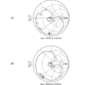
- FIG. 2 shows characteristics of the SAW filter 11 and the SAW filter 12, and characteristic changes when a transmission line having a line length set for reflection phase adjustment is arranged between the switch element 20 and each SAW filter.
- a dotted line indicates a reflection characteristic when the SAW filter is viewed from the switch element 20 when each SAW filter is connected, and a solid line indicates a reflection characteristic when the SAW filter is viewed from the switch element 20 when a transmission line is added. It is.
- the markers described in each Smith chart indicate the reflection phase at the frequency of the GPS signal, the inverted black triangle ( ⁇ ) marker indicates the reflection phase of the SAW filter alone, and the inverted white triangle ( ⁇ ) marker indicates the transmission line. This is the reflection phase when arranged.
- FIG. 2A shows the reflection characteristics of the SAW filter 11
- FIG. 2B shows the reflection characteristics of the SAW filter 12.
- the reflection phase of the SAW filter alone is the SAW filter 11.
- the SAW filter 12 is closer to the short side in the Smith chart. Therefore, when two SAW filters having such reflection characteristics are used, the SAW filter 12 is disposed closer to the switch element 20 than the SAW filter 11, and the switch element 20 and the SAW filter 12 are disposed between the SAW filter 12 and the SAW filter 12.
- the transmission line 101 between the switch element 20 and the SAW filter 11 is formed longer than the transmission line 102.
- the reflection phase at the frequency of the GPS signal when the SAW filter 11 side is viewed from the switch element 20 changes to the short side in the Smith chart.
- the transmission line 102 between the switch element 20 and the SAW filter 12 is formed shorter than the transmission line 101, the GPS signal frequency when the SAW filter 12 side is viewed from the switch element 20 is used. The amount of change is smaller than the reflection phase when the SAW filter 11 is seen.
- the reflection phase characteristic of the SAW filter alone with respect to the GPS signal can be reduced to SAW. Further significant deterioration of the reflection phase of the SAW filter 12 worse than the filter 11 is suppressed, and the reflection phase characteristic of the SAW filter 11 with respect to the GPS signal in the SAW filter alone is better than that of the SAW filter 12. It can be suppressed to about the phase.
- the degree of deterioration of the reflection phase of the SAW filter 11 with respect to the GPS signal is less than the degree of deterioration of the reflection phase of the SAW filter 12 with respect to the GPS signal, in consideration of the line length of the transmission line that is substantially negligible in circuit formation.
- the reflection phase characteristic with respect to the GPS signal as the high frequency switch module 1 can be improved.
- FIG. 3 shows a case where the transmission line 101 has a line length longer than that of the transmission line 102 in the case of the Smith chart characteristics as shown in FIG.
- the antenna connection port ANT0 and the communication signal input / output port P3 (GPS signal input / output port) when the transmission line 102 is shorter when the transmission line 102 is longer than the transmission line 101.
- FIG. 6 is a characteristic diagram showing pass characteristics.
- the solid line indicates a case where the line length of the transmission line 101 is shorter than the line length of the transmission line 102
- the dotted line indicates a case where the transmission line 101 is longer than the transmission line 102.
- the transmission characteristics are improved by making the transmission line 101 longer than the transmission line 102.
- the line lengths of these transmission lines 101 and 102 do not take into account only the frequency band of the GPS signal, but the phase adjustment between the switch element 20 and the SAW filter 11 for the GSM1900 communication signal and the switch element for the GSM1800 communication signal. 20 is set in consideration of the phase adjustment between the SAW filter 12 and the SAW filter 12. Thereby, favorable pass characteristics can be obtained for each of the GPS signal, the GSM1900 communication signal, and the GSM1800 communication signal.
- the improvement of the reflection phase and the passing characteristic as described above can be realized by using only the two transmission lines 101 and 102 and adjusting the lengths of these lines.
- a high-frequency switch module with good characteristics capable of transmitting and receiving communication signals in a plurality of frequency bands to one antenna can be realized with a simple configuration and a small size.
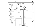
- FIG. 4 is a mounting diagram showing a schematic configuration of the high-frequency switch module 1 of the present embodiment.
- the high-frequency switch module 1 of this embodiment is realized by an electrode pattern and a mounting component formed on a laminated circuit board formed by laminating a plurality of insulating layers. Specifically, electrode patterns constituting the above-described circuit pattern are formed on the top surface 1U and the inner layer of the laminated circuit board. Further, on the top surface 1U of the multilayer circuit board, mounting lands for various discrete components for realizing the circuit of the above-described high-frequency switch module 1 are formed. At this time, the mounting land for the switch element 20 is formed so as to be close to the mounting land for the SAW filter 12, and the mounting land for the SAW filter 11 is the mounting land for the switch element 20 and the SAW filter 12. It is formed away from. Further, on the top surface 1U of the multilayer circuit board, lands for mounting the SAW filters 13 and 14 are formed, and further, lands for mounting capacitors and inductors constituting the circuit shown in FIG. 1 are formed. .
- the switch element 20 is mounted on the land for the switch element 20, the SAW filters 11 to 14 are mounted on the lands for the SAW filters 11 to 14, respectively, and the lands for capacitors and inductors are respectively corresponding to the lands. Capacitors and inductors composed of discrete chip components are mounted. The inductor and the capacitor may be realized by an inner layer electrode of the multilayer circuit board.
- the land for the first selection port 201 of the switch element 20 and the land of the connection terminal 111 to the switch element 20 of the SAW filter 11 are connected by an electrode pattern, thereby the transmission line 101 of FIG. Is formed.
- the land for the second selection port 202 of the switch element 20 and the land of the connection terminal 121 to the switch element 20 of the SAW filter 12 are connected by an electrode pattern, whereby the transmission line 102 of FIG. It is formed.
- the land for the switch element 20 and the land for the SAW filter 12 are formed close to each other, and the land for the SAW filter 11 is formed so as to be separated from the land, so that the electrode pattern forming the transmission line 101 is formed. Is longer than the electrode pattern forming the transmission line 102.
- the line length of the transmission line 101 can be made longer than the line length of the transmission line 102 as described above, and the high-frequency switch can be set by appropriately setting each line length while maintaining this short / long relationship.
- the reflection phase and the pass characteristic with respect to the GPS signal as the module 1 can be improved.
- the electrode pattern forming the transmission line 101 and the electrode pattern forming the transmission line 102 are formed on the top surface 1U of the laminated circuit board, these electrode patterns are arranged on the electrode surface along the laminating direction. It does not have a shape that faces each other. Accordingly, the isolation between the electrode pattern forming the transmission line 101 and the electrode pattern forming the transmission line 102 is improved, and more excellent reflection phase characteristics and transmission characteristics can be realized, and there is no need to consider the stray capacitance. It becomes easy to design so as to obtain such characteristics.
- the SAW filter 11 and the SAW filter 12 are arranged apart from each other, the isolation between these SAW filters can be improved.
- the SAW filter 13 different from these is disposed between the SAW filter 11 and the SAW filter 12 on the mounting surface, the electromagnetic field between the elements between the first filter element and the second filter element. Coupling and electromagnetic coupling between mounting lands are further suppressed. Thereby, the isolation between the SAW filter 11 and the SAW filter 12 can be further improved.
- FIG. 5 is a mounting diagram for explaining the pattern of the transmission line 101 ′ using the inner layer electrode of the multilayer circuit board.
- the transmission line 101 ′ whose line length should be relatively long includes an electrode pattern portion formed on the top surface 1 ⁇ / b> U, a portion formed by the inner layer electrode, and a via hole connecting these in the stacking direction. It consists of.
- the transmission line 102 'whose line length should be relatively short is composed of an electrode pattern formed only on the top surface 1U. In the case of such a configuration, the transmission line 102 ′ and the transmission line 101 ′ can be routed so as not to contact each other while intersecting when viewed from the top surface 1 ⁇ / b> U side. As a result, as shown in FIG.
- Lines 101 ′ and 102 ′ can be formed. Furthermore, by forming the transmission line 101 ′ in a plurality of layers and forming the transmission line 102 ′ only in one layer, it is easy to increase the line length of the transmission line 101 ′ relative to the transmission line 102 ′. Thereby, the design and formation of the transmission lines 101 ′ and 102 ′ can be facilitated.
- the transmission line 101 ′ is formed in a plurality of layers, and the transmission line 101 ′ and the transmission line 102 ′ are not crossed in the stacking direction, thereby improving the isolation between the transmission lines. You can also.
- the filter circuit includes a plurality of filter elements each having a different frequency band as a pass band, a switch circuit, and a diplexer. If it is a high frequency switch module, the above-mentioned composition is applicable.
- the GSM1900 communication signal, the GSM1800 communication signal, the GPS signal, and the GSM850 communication signal are switched as an example by a single antenna, but other frequency combinations may be used.
- 1-high frequency switch module 11-14-SAW filter, 20-switch element, 30, 40-diplexer, 101, 101 ', 102, 102'-transmission line, 1U-top surface of laminated circuit board
Landscapes
- Engineering & Computer Science (AREA)
- Computer Networks & Wireless Communication (AREA)
- Signal Processing (AREA)
- Physics & Mathematics (AREA)
- Acoustics & Sound (AREA)
- Transceivers (AREA)
- Filters And Equalizers (AREA)
- Surface Acoustic Wave Elements And Circuit Networks Thereof (AREA)
Abstract
Description
図1は本実施形態の高周波スイッチモジュール1の回路図である。
Claims (6)
- 一つのアンテナを用いてそれぞれに異なる複数種類の周波数帯域からなる通信信号を送受信する高周波モジュールであって、
第1周波数帯域通信信号および第2周波数帯域通信信号と、第3周波数帯域通信信号とを分波するダイプレクサと、
前記第1周波数帯域信号の送受信と前記第2周波数帯域信号の送受信とを切り替えるスイッチ素子と、
前記第1周波数帯域信号の入出力ポートと前記スイッチ素子との間に挿入され、前記第1周波数帯域を通過する第1フィルタ素子、および前記第2周波数帯域信号の入出力ポートと前記スイッチ素子との間に挿入され、前記第2周波数帯域を通過する第2フィルタ素子と、
前記スイッチ素子から見た前記第1フィルタ素子単体の前記第3周波数帯域での第1反射位相と前記スイッチ素子から見た前記第2フィルタ素子単体の前記第3周波数帯域での第2反射位相とが、ともにスミスチャート上における容量性であって、且つ第2反射位相が第1反射位相に対して、スミスチャート上でショート側に存在する場合に、
前記スイッチ素子と前記第1フィルタ素子とを接続する第1伝送線路の線路長は、前記スイッチ素子と前記第2フィルタ素子とを接続する第2伝送線路の線路長よりも長い、高周波モジュール。 - 請求項1に記載の高周波モジュールであって、
前記ダイプレクサは、回路基板に実装された素子および該回路基板に形成された回路電極パターンにより形成され、
前記スイッチ素子、前記第1フィルタ素子、および前記第2フィルタ素子は、前記回路基板上に実装される実装型素子であり、
前記第1伝送線路と前記第2伝送線路とは、前記回路基板を前記実装型素子の実装面側から見て、前記回路基板の異なる位置に形成された電極パターンからなる、高周波モジュール。 - 請求項1または請求項2に記載の高周波モジュールであって、
前記ダイプレクサは、回路基板に実装された素子および該回路基板に形成された回路電極パターンにより形成され、
前記スイッチ素子、前記第1フィルタ素子、および前記第2フィルタ素子は、前記回路基板上に実装される実装型素子であり、
前記第2伝送線路は前記回路基板の前記実装型素子の実装面に形成された電極パターンからなり、
前記第1伝送線路は前記回路基板の前記実装型素子の実装面に形成された電極パターンと内装された電極パターンとにより形成される、高周波モジュール。 - 請求項1乃至請求項3のいずれかに記載の高周波モジュールであって、
前記第1フィルタ素子と前記第2フィルタ素子とは、前記実装面の離間した位置に実装されている、高周波モジュール。 - 請求項1乃至請求項4のいずれかに記載の高周波モジュールであって、
前記第1フィルタ素子および前記第2フィルタ素子は、SAWフィルタである、高周波モジュール。 - 請求項1乃至請求項5のいずれかに記載の高周波モジュールであって、
前記回路基板の前記実装面における前記第1フィルタ素子と前記第2フィルタ素子との間に、第3フィルタ素子が配置されている、高周波モジュール。
Priority Applications (4)
| Application Number | Priority Date | Filing Date | Title |
|---|---|---|---|
| DE112010001932.0T DE112010001932B4 (de) | 2009-06-19 | 2010-06-18 | Hochfrequenzmodul |
| JP2011519846A JP5234182B2 (ja) | 2009-06-19 | 2010-06-18 | 高周波モジュール |
| CN201080027209.7A CN102804599B (zh) | 2009-06-19 | 2010-06-18 | 高频模块 |
| US13/326,387 US8861498B2 (en) | 2009-06-19 | 2011-12-15 | High-frequency module |
Applications Claiming Priority (2)
| Application Number | Priority Date | Filing Date | Title |
|---|---|---|---|
| JP2009-145963 | 2009-06-19 | ||
| JP2009145963 | 2009-06-19 |
Related Child Applications (1)
| Application Number | Title | Priority Date | Filing Date |
|---|---|---|---|
| US13/326,387 Continuation US8861498B2 (en) | 2009-06-19 | 2011-12-15 | High-frequency module |
Publications (1)
| Publication Number | Publication Date |
|---|---|
| WO2010147197A1 true WO2010147197A1 (ja) | 2010-12-23 |
Family
ID=43356513
Family Applications (1)
| Application Number | Title | Priority Date | Filing Date |
|---|---|---|---|
| PCT/JP2010/060329 Ceased WO2010147197A1 (ja) | 2009-06-19 | 2010-06-18 | 高周波モジュール |
Country Status (5)
| Country | Link |
|---|---|
| US (1) | US8861498B2 (ja) |
| JP (1) | JP5234182B2 (ja) |
| CN (1) | CN102804599B (ja) |
| DE (1) | DE112010001932B4 (ja) |
| WO (1) | WO2010147197A1 (ja) |
Families Citing this family (5)
| Publication number | Priority date | Publication date | Assignee | Title |
|---|---|---|---|---|
| US6217832B1 (en) | 1998-04-30 | 2001-04-17 | Catalytica, Inc. | Support structures for a catalyst |
| JP6024702B2 (ja) * | 2014-05-02 | 2016-11-16 | 株式会社村田製作所 | 回路基板及び分波回路 |
| CN104617972A (zh) * | 2014-12-30 | 2015-05-13 | 宇龙计算机通信科技(深圳)有限公司 | 传输信号的方法、装置及终端 |
| JP6465210B2 (ja) * | 2015-06-24 | 2019-02-06 | 株式会社村田製作所 | 分波回路 |
| EP4080773A1 (de) * | 2021-04-19 | 2022-10-26 | Siemens Aktiengesellschaft | Hochfrequenz-filter |
Citations (5)
| Publication number | Priority date | Publication date | Assignee | Title |
|---|---|---|---|---|
| JP2002141764A (ja) * | 2000-11-01 | 2002-05-17 | Hitachi Metals Ltd | 周波数分波回路、およびアンテナスイッチ積層モジュール複合部品 |
| JP2004032673A (ja) * | 2002-03-27 | 2004-01-29 | Tdk Corp | フロントエンドモジュール |
| JP2004040322A (ja) * | 2002-07-01 | 2004-02-05 | Tdk Corp | 無線通信回路 |
| JP2005268878A (ja) * | 2004-03-16 | 2005-09-29 | Matsushita Electric Ind Co Ltd | アンテナ共用器 |
| JP2006211057A (ja) * | 2005-01-25 | 2006-08-10 | Oki Electric Ind Co Ltd | トリプレクサ |
Family Cites Families (7)
| Publication number | Priority date | Publication date | Assignee | Title |
|---|---|---|---|---|
| US7057472B2 (en) * | 2001-08-10 | 2006-06-06 | Hitachi Metals, Ltd. | Bypass filter, multi-band antenna switch circuit, and layered module composite part and communication device using them |
| JP2003087076A (ja) | 2001-09-07 | 2003-03-20 | Murata Mfg Co Ltd | チップ状lc複合部品およびそれを用いた回路 |
| US7076216B2 (en) * | 2002-09-17 | 2006-07-11 | Hitachi Metals, Ltd. | High-frequency device, high-frequency module and communications device comprising them |
| US7373171B2 (en) * | 2003-02-14 | 2008-05-13 | Tdk Corporation | Front end module |
| JP2005260837A (ja) | 2004-03-15 | 2005-09-22 | Ngk Spark Plug Co Ltd | アンテナ切換モジュールおよびその設計方法 |
| US6963257B2 (en) | 2004-03-19 | 2005-11-08 | Nokia Corporation | Coupled BAW resonator based duplexers |
| JP2006108824A (ja) | 2004-09-30 | 2006-04-20 | Tdk Corp | トリプレクサ |
-
2010
- 2010-06-18 DE DE112010001932.0T patent/DE112010001932B4/de not_active Expired - Fee Related
- 2010-06-18 JP JP2011519846A patent/JP5234182B2/ja not_active Expired - Fee Related
- 2010-06-18 WO PCT/JP2010/060329 patent/WO2010147197A1/ja not_active Ceased
- 2010-06-18 CN CN201080027209.7A patent/CN102804599B/zh not_active Expired - Fee Related
-
2011
- 2011-12-15 US US13/326,387 patent/US8861498B2/en active Active
Patent Citations (5)
| Publication number | Priority date | Publication date | Assignee | Title |
|---|---|---|---|---|
| JP2002141764A (ja) * | 2000-11-01 | 2002-05-17 | Hitachi Metals Ltd | 周波数分波回路、およびアンテナスイッチ積層モジュール複合部品 |
| JP2004032673A (ja) * | 2002-03-27 | 2004-01-29 | Tdk Corp | フロントエンドモジュール |
| JP2004040322A (ja) * | 2002-07-01 | 2004-02-05 | Tdk Corp | 無線通信回路 |
| JP2005268878A (ja) * | 2004-03-16 | 2005-09-29 | Matsushita Electric Ind Co Ltd | アンテナ共用器 |
| JP2006211057A (ja) * | 2005-01-25 | 2006-08-10 | Oki Electric Ind Co Ltd | トリプレクサ |
Also Published As
| Publication number | Publication date |
|---|---|
| US20120087285A1 (en) | 2012-04-12 |
| DE112010001932B4 (de) | 2018-08-02 |
| CN102804599B (zh) | 2016-03-16 |
| CN102804599A (zh) | 2012-11-28 |
| US8861498B2 (en) | 2014-10-14 |
| DE112010001932T5 (de) | 2012-11-08 |
| JPWO2010147197A1 (ja) | 2012-12-06 |
| JP5234182B2 (ja) | 2013-07-10 |
Similar Documents
| Publication | Publication Date | Title |
|---|---|---|
| KR101271108B1 (ko) | 듀플렉서 모듈 | |
| JP6168243B2 (ja) | 移相器、インピーダンス整合回路、合分波器および通信端末装置 | |
| US8644197B2 (en) | RF front-end module and antenna systems | |
| JP5720854B2 (ja) | アンテナマッチングデバイス | |
| US8390392B2 (en) | Variable capacitance module and matching circuit module | |
| WO2008004557A1 (fr) | Circuit en dérivation, circuit haute fréquence et module haute fréquence | |
| WO2019082671A1 (ja) | 高周波回路、マルチプレクサ、高周波フロントエンド回路および通信装置 | |
| US10454450B2 (en) | High frequency switch module | |
| US9319092B2 (en) | High-frequency module | |
| JP5234182B2 (ja) | 高周波モジュール | |
| JP2002118486A (ja) | 高周波複合スイッチモジュール | |
| US10734970B2 (en) | Phase shifter module, multiplexer/demultiplexer, and communication apparatus | |
| JP6311787B2 (ja) | 高周波モジュール | |
| US10348268B2 (en) | Demultiplexing circuit | |
| JP5874501B2 (ja) | 高周波モジュール | |
| JP2010212962A (ja) | 高周波部品およびそれを用いた通信装置 | |
| KR102223448B1 (ko) | 고주파 스위치 모듈 | |
| JP2004241875A (ja) | アンテナスイッチ | |
| JP4135936B2 (ja) | 高周波モジュールおよび高周波回路 | |
| JP2005175655A (ja) | 高周波部品 |
Legal Events
| Date | Code | Title | Description |
|---|---|---|---|
| WWE | Wipo information: entry into national phase |
Ref document number: 201080027209.7 Country of ref document: CN |
|
| 121 | Ep: the epo has been informed by wipo that ep was designated in this application |
Ref document number: 10789570 Country of ref document: EP Kind code of ref document: A1 |
|
| WWE | Wipo information: entry into national phase |
Ref document number: 2011519846 Country of ref document: JP |
|
| WWE | Wipo information: entry into national phase |
Ref document number: 112010001932 Country of ref document: DE Ref document number: 1120100019320 Country of ref document: DE |
|
| 122 | Ep: pct application non-entry in european phase |
Ref document number: 10789570 Country of ref document: EP Kind code of ref document: A1 |