WO2010143530A1 - 窓ガラス破損センサ、窓ガラス破損センサフィルム、及び窓ガラス破損センサフィルムの製造方法 - Google Patents
窓ガラス破損センサ、窓ガラス破損センサフィルム、及び窓ガラス破損センサフィルムの製造方法 Download PDFInfo
- Publication number
- WO2010143530A1 WO2010143530A1 PCT/JP2010/058785 JP2010058785W WO2010143530A1 WO 2010143530 A1 WO2010143530 A1 WO 2010143530A1 JP 2010058785 W JP2010058785 W JP 2010058785W WO 2010143530 A1 WO2010143530 A1 WO 2010143530A1
- Authority
- WO
- WIPO (PCT)
- Prior art keywords
- conductive layer
- glass plate
- film
- layer
- window
- Prior art date
- Legal status (The legal status is an assumption and is not a legal conclusion. Google has not performed a legal analysis and makes no representation as to the accuracy of the status listed.)
- Ceased
Links
Images













Classifications
-
- G—PHYSICS
- G08—SIGNALLING
- G08B—SIGNALLING SYSTEMS, e.g. PERSONAL CALLING SYSTEMS; ORDER TELEGRAPHS; ALARM SYSTEMS
- G08B13/00—Burglar, theft or intruder alarms
- G08B13/02—Mechanical actuation
- G08B13/04—Mechanical actuation by breaking of glass
Definitions
- the present invention relates to a window glass break sensor, a window glass break sensor film, and a method for manufacturing a window glass break sensor film.
- Patent Document 1 discloses a conductor wiring film that can be applied to adherends of various sizes while maintaining the beauty of the adherend.
- the conductor wiring film of patent document 1 can detect the presence or absence of the damage of a to-be-adhered body, and can perform defrosting and anti-fogging of an to-be-adhered body.
- the conductor wiring film includes a resin film and a conductor.
- the resin film has an adhesive layer on its main surface.
- the conductor has a plurality of straight portions and curved portions, and the straight portions and the curved portions are disposed in the adhesive layer.
- the straight portions of the conductors are arranged substantially parallel to each other, and the curved portion and the straight portion are connected to each other so as to meander as a whole.
- a connection terminal is connected to each curved portion in any one of the two curved portion rows arranged in a straight line.
- Patent Document 1 describes that the outer diameter of the conductor is preferably 10 to 100 ⁇ m.
- the conductor for detecting glass breakage is a metal wire having a uniform density of 10 ⁇ m or more in diameter, and has a property of extending relatively well. Therefore, even if a micro crack occurs in the glass, the conductor is not disconnected, so that the breakage of the glass cannot be detected.
- the conductor wiring film of the said patent document 1 is low sensitivity as a glass breakage sensor. In order to improve the detection sensitivity, it is necessary to provide a conductor wiring film over the entire surface of the glass. Moreover, since the conductor wiring film of the said patent document 1 needs to arrange
- An object of the present invention is to provide a window glass break sensor, a window glass break sensor film, and a method for manufacturing a window glass break sensor film that can reliably detect breakage of glass.
- a window glass breakage sensor including a conductive layer, an adhesive layer, and a detection unit.
- the conductive layer is disposed on the surface of the glass plate applied to the window.
- the conductive layer is patterned by printing.
- the adhesive layer attaches the conductive layer to the glass plate.
- the detection unit detects breakage of the glass plate by cutting the conductive layer or changing resistance.
- a window glass breakage sensor film to be attached to a glass plate of a window.
- the sensor film includes a base film, a conductive layer, and an adhesive layer.
- the base film supports the printed material.
- the conductive layer is disposed on the base film.
- the conductive layer is patterned by printing.
- the conductive layer detects breakage of the glass plate by its own cutting or resistance change.
- the adhesive layer is disposed on the base film.
- the adhesive layer is formed by printing. The adhesive layer attaches the conductive layer to the glass plate.
- a method for producing a window glass breakage sensor film includes a step of preparing a base film for supporting a printed matter, and a patterning of the conductive layer on the base film for supporting the printed matter by printing on the printed film supporting base film for detecting breakage of the glass plate of the window by cutting or resistance change. And a step of forming an adhesive layer on the conductive layer by printing.
- FIG. 4 is a cross-sectional view taken along line 4-4 of FIG. (A)-(e) is sectional drawing which shows the manufacturing method of a sensor film, respectively.
- (A), (b) is sectional drawing for demonstrating the attachment process to the glass plate of a sensor film, respectively. Sectional drawing of a sensor film. The figure which shows the modification of 1st Embodiment.
- FIG. 17 is a cross-sectional view taken along line 17-17 in FIG. Sectional drawing of the sensor film in the 5th Embodiment of this invention.
- (A)-(f) is a conceptual diagram of the conductive layer for demonstrating 7th Embodiment, respectively.
- (A)-(c) is a conceptual diagram of the conductive layer for demonstrating 7th Embodiment, respectively.
- (A)-(f) is sectional drawing of the sensor film for demonstrating 7th Embodiment, respectively.
- the triangular window 12 as a window for motor vehicles is provided in the left-right both sides (only the left side is shown) in the rear part of the vehicle 11.
- These triangular windows 12 are windows that cannot be opened and closed.
- the glass plate 13 of the triangular window 12 is a window glass formed so that a crack will be generated as a whole when a part thereof is broken.
- the glass plate 13 is tempered glass.
- FIG. 1 (b) is a cross-sectional view of a portion near the triangular window 12 along the line 1b-1b in FIG. 1 (a).
- the glass plate 13 of the triangular window 12 is fixed to the vehicle body 15 via an adhesive (glass adhesive) 14 at the peripheral edge of the glass plate 13.
- the glass plate 13 has a thickness of about 3.1 mm to 5.0 mm.
- the window glass break sensor 20 is a sensor that detects breakage of the glass plate 13 of the window for an automobile.
- the film 30 is covered with an interior 16 of the vehicle 11.
- FIG. 2 shows a plane and a cross section of the sensor film 30.
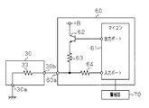
- FIG. 3 is an electrical configuration diagram of the window glass breakage sensor 20.
- 4 is a cross-sectional view taken along line 4-4 of FIG. 5A to 5E are cross-sectional views showing a method for manufacturing the sensor film 30.
- FIG. 5A to 5E are cross-sectional views showing a method for manufacturing the sensor film 30.
- the window glass break sensor 20 includes a sensor film 30, a determination circuit 60, and an alarm device 70.
- the sensor film 30 has a rectangular shape as a planar structure.
- the sensor film 30 is a laminated body including an adhesive layer 31, an insulating layer 32, a conductive layer 33, and an insulating layer 34 as a cross-sectional structure.
- the insulating layers 32 and 34 are made of resin.
- the insulating layer 32 functions as a base member, and the insulating layer 34 functions as a surface protective film.
- the conductive layer 33 has one fine wire portion 33a and electrodes 33b and 33c formed at both ends of the fine wire portion 33a.
- the fine wire portion 33 a is disposed on the glass plate 13 via the adhesive layer 31 and the insulating layer 32.
- the fine line portion 33a is patterned so as to extend linearly by printing. That is, the thin sensor film 30 has the conductive layer 33 having the fine line portion 33a patterned by printing in the inside (inside a plurality of laminated sheet materials).
- the thin wire portion 33a extends in a direction extending in the direction in which the crack generated when the glass plate 13 breaks in FIG. 2 or the direction X in which the crack extends (preferably in a direction substantially orthogonal), and a plurality of the thin wire portions 33a.
- the pattern is folded back.
- the line width of the fine line portion 33a is about 200 ⁇ m.
- the thin wire portion 33a is a fine pattern and is easily disconnected.
- the electrodes 33b and 33c formed at both ends of the fine wire portion 33a are wider than the fine wire portion 33a.
- Openings 34a and 34b are formed in the insulating layer 34 on the electrodes 33b and 33c, and the electrodes 33b and 33c are exposed through the openings 34a and 34b.
- the openings 34a and 34b serve as electrode extraction portions.
- a conductive layer 33 is attached to the glass plate 13 by the adhesive layer 31.
- the conductive layer 33 having the electrodes 33b and 33c is formed on the glass plate 13.
- One end of the wire harness 50 is connected to one of the electrodes 33b and 33c in FIG. 2 via the connector C as shown in FIG. 1B, and a determination circuit 60 is connected to the other end of the wire harness 50.
- the conductive layer 33 of the sensor film 30 is cut or the resistance of the conductive layer 33 is changed due to the minute crack. Breakage of the glass plate 13 is detected by cutting the conductive layer 33 or changing the resistance.
- the sensor film 30 since the sensor film 30 is affixed to the glass plate 13, it is not necessary to directly print the conductive layer 33 on the glass plate 13, so that the cost can be reduced.
- the sensor film 30 can be attached later to the glass plate 13 without the conductive layer 33.
- the sensor film 30 since the sensor film 30 includes the conductive layer 33 made of a thin wire, it is possible to detect breakage of the glass plate 13 even if the glass plate 13 is not completely crushed.
- the determination circuit 60 includes a microcomputer 61, a transistor 62, and resistors 63 and 64.
- the input port of the microcomputer 61 is connected to the connection terminal 60 a of the determination circuit 60 through the resistor 64.
- Transistor (npn transistor) 62 has a collector connected to power supply terminal + B and an emitter connected to connection terminal 60a through resistor 63.
- the base of the transistor 62 is connected to the output port of the microcomputer 61.
- an alarm device 70 is connected to the microcomputer 61.
- a plastic film 40 that functions as a support for a printed material is prepared.
- the plastic film 40 as a base film for supporting the printed material has the same shape and dimensions as the sensor film 30.
- the plastic film 40 is any one selected from polyethylene terephthalate (PET), polyethylene naphthalate (PEN), acrylic, polycarbonate (PC), polyimide (PI), liquid crystal polymer (LCP), and polyarylate (PAR). It is formed using resin.
- PET polyethylene terephthalate
- PEN polyethylene naphthalate
- acrylic polycarbonate
- PI polyimide
- LCP liquid crystal polymer
- PAR polyarylate
- polyimide (PI), liquid crystal polymer (LCP), and polyarylate (PAR) are preferable from the viewpoint of heat resistance.
- an insulating layer 34 is formed on the plastic film 40 by screen printing. Thereafter, the insulating layer 34 is heated. Further, as shown in FIG. 5C, the conductive layer 33 is patterned on the insulating layer 34 by screen printing. Thereafter, the conductive layer 33 is heated.
- the conductive layer 33 is placed in any one type of resin selected from thermosetting polyester-based, urethane-based, rubber-based, polyimide-based, epoxy-based, and phenol-based resins. It is formed using a printing ink made of dispersed conductive particles (for example, silver particles). That is, the conductive layer 33 includes a large number of conductive particles that are electrically connected to each other by a resin as a binder.
- the conductive particles may be carbon particles instead of silver particles, and various metal particles such as copper (Cu) particles, nickel (Ni) particles, palladium (Pd) particles, and alloy particles. Can be used.
- the conductive layer 33 may be formed using a printing ink containing both silver particles and carbon particles.
- an insulating layer 32 is formed on the insulating layer 34 so as to cover the conductive layer 33 by screen printing. Thereafter, the insulating layer 32 is heated. Then, as shown in FIG. 5E, an adhesive layer 31 is formed on the insulating layer 32 by screen printing. Thereafter, the adhesive layer 31 is heated.
- the sensor film 30 has an insulating layer 34 between the conductive layer 33 and the plastic film (base film) 40.
- the insulating layer 34 is one of printing inks selected from thermosetting or ultraviolet curable polyester printing ink, acrylic printing ink, acrylic urethane printing ink, urethane printing ink, and polyimide printing ink. Formed using.
- the sensor film 30 has an insulating layer 32 between the adhesive layer 31 and the conductive layer 33.
- the insulating layer 32 is one of printing inks selected from thermosetting or ultraviolet curable polyester printing ink, acrylic printing ink, acrylic urethane printing ink, urethane printing ink, and polyimide printing ink. Formed using.
- binder material that electrically connects the conductive particles in the conductive layer 33 examples include polyester-based, acrylic-based, acrylic-urethane-based, urethane-based, and polyimide-based resins.
- the binder in the conductive layer 33 can use the following materials from the viewpoint of having insulating properties. That is, as the binder in the conductive layer 33, an acrylic resin, copolymerized polyester, polyurethane, or polyvinyl acetate copolymer can be used as the evaporation drying type binder.
- an epoxy resin, a phenol resin, a copolymerized polyester, a polyurethane, or a vinyl chloride vinyl acetate copolymer can be used as a thermosetting binder.
- an acrylic resin or an acrylic urethane resin can be used as the UV curable indender.
- a vinyl resin, an epoxy resin, a phenol resin, an olefin resin, or a silicone resin can be used as the binder in the conductive layer 33.
- a thermoplastic resin, a thermosetting resin, a UV curable resin, or the like can be used as the binder in the conductive layer 33.
- the thickness of the plastic film 40 is about 50 to several hundred ⁇ m
- the thickness of the adhesive layer 31 is about several ⁇ m (for example, 6 ⁇ m)
- the thickness of the insulating layer 32 is about several ⁇ m
- the thickness of the conductive layer 33 is about several ⁇ m (for example, 3 ⁇ m)
- the thickness of the insulating layer 34 is about several ⁇ m (for example, 3 ⁇ m).
- the adhesive layer 31 of the sensor film 30 is attached to one surface (glass surface) of the glass plate 13 as shown in FIG.
- the sensor film 30 is attached to the glass plate 13 by the contact layer 31 by contact.
- thermosetting adhesive can be used as the adhesive layer 31.
- a double-sided tape may be used as the adhesive layer 31, and an acrylic non-carrier pressure-sensitive adhesive, a rubber-based pressure-sensitive adhesive, a silicone-based pressure-sensitive adhesive, or a vinyl-based pressure-sensitive adhesive may be used as the pressure-sensitive adhesive for this double-sided tape.
- the sensor film 30 is attached to the glass plate 13 as shown in FIG. In this way, the sensor film 30 is a transfer type in which only the printed film remains by being peeled from the plastic film 40 when being attached to the glass plate 13.
- FIG. 7 is a cross-sectional view of a portion corresponding to line 7-7 in FIG.
- FIG. 7 shows a cross-sectional view of the conductive layer 33 cut by a crack extending in a direction orthogonal to the extending direction of the conductive layer 33.
- the microcomputer 61 of the determination circuit 60 in FIG. 3 turns the transistor 62 on by setting the output port to the H level at regular intervals. Then, the microcomputer 61 determines whether the potential level of the input port is higher than a predetermined potential. When the conductive layer 33 of the sensor film 30 is not cut or a part of the conductive layer 33 is not cracked, the resistance value does not increase and the potential level of the microcomputer input port is always the ground level. If the potential level of the input port is the ground level when the transistor 62 is turned on, the microcomputer 61 determines that the glass plate 13 is not damaged and is normal.
- the microcomputer 61 determines that the glass plate 13 is broken if the potential level of the input port is not the ground level when the transistor 62 is turned on. Then, the microcomputer 61 notifies the outside that the glass plate 13 is broken (an abnormality has occurred) by an alarm sound or an alarm lamp at the alarm device 70.
- the window glass break sensor 20 affixes the conductive layer 33 patterned to extend linearly on the surface of the glass plate 13 and the conductive layer 33 to the glass plate 13.
- the adhesive layer 31 is provided.
- the window glass break sensor 20 detects breakage of the glass plate 13 by a change in resistance of the conductive layer 33.
- the sensor film 30 includes a conductive layer 33 patterned on the plastic film 40 so as to extend linearly by printing, and a conductive layer formed by printing on the plastic film 40. And an adhesive layer 31 for attaching 33 to the glass plate 13.
- FIG. 4 the window glass break sensor 20 affixes the conductive layer 33 patterned to extend linearly on the surface of the glass plate 13 and the conductive layer 33 to the glass plate 13.
- the adhesive layer 31 is provided.
- the window glass break sensor 20 detects breakage of the glass plate 13 by a change in resistance of the conductive layer 33.
- the sensor film 30 includes a conductive layer 33 patterned on the plastic film 40 so as to extend linearly by printing, and
- the manufacturing method of the sensor film 30 includes a conductive layer patterning step of patterning the conductive layer 33 so as to extend linearly by printing on a plastic film 40 as a base film, and a conductive layer. And an adhesive layer forming step of forming the adhesive layer 31 on the 33 by printing.
- the conductor is formed by printing without depending on the wiring, and the breakage of the glass plate 13 can be reliably detected.
- the conductive layer 33 extends in the direction X substantially perpendicular to the direction of cracks generated when the glass plate 13 is broken or the direction in which the cracks extend. This is preferable for detecting breakage of the plate 13.
- the plastic film 40 is peeled off from the sensor film 30 after the sensor film 30 is attached to the glass plate 13, so that the sensor film 30 has high sensitivity.
- a pressure-sensitive adhesive that presses and adheres the sensor film 30 to the glass plate 13 when the sensor film 30 is attached to the glass plate 13 may be used. Further, as the adhesive layer 31, when the sensor film 30 is attached to the glass plate 13, at least one of the sensor film 30 and the glass plate 13 is heated and the sensor film 30 is pressed against the glass plate 13 to be bonded. An adhesive may be used. Further, as the adhesive layer 31, an induction heating type adhesive that adheres the sensor film 30 to the glass plate 13 by induction heating at least one of the sensor film 30 and the glass plate 13 when the sensor film 30 is attached to the glass plate 13. May be used.
- active energy rays (electron beam, X-ray, ultraviolet ray, visible ray, infrared ray, etc.) are applied to at least one of the sensor film 30 and the glass plate 13.
- An adhesive (such as a UV adhesive) that cures by irradiation and bonds the sensor film 30 to the glass plate 13 may be used.
- the sensor film 30 of the window glass breakage sensor 20 of the present embodiment has a structure shown in FIGS.
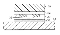
- the insulating layer 34 is formed on the plastic film 40 in the sensor film 30 in the present embodiment in a state before being attached to the glass plate 13.
- a conductive layer 33 is patterned on the insulating layer 34, and an adhesive layer 31 is formed on the conductive layer 33 and the insulating layer 34.
- the sensor film 30 shown in FIG. 9 is attached to the glass plate 13 of the vehicle as shown in FIG. That is, the adhesive layer 31 of the sensor film 30 is brought into contact with one surface (glass surface) of the glass plate 13, and the sensor film 30 is attached to the glass plate 13 by the adhesive layer 31. Thereafter, when the plastic film 40 is peeled off from the sensor film 30, the sensor film 30 is attached to the glass plate 13.
- FIG. 10 the plastic film 40 of FIG. 9 is peeled off from the sensor film 30, but as shown in FIG. 11, the sensor film 30 may be used as it is without peeling off the plastic film 40 of FIG.
- the sensor film 30 of the window glass breakage sensor 20 of the present embodiment has a structure shown in FIGS.
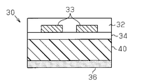
- the sensor film 30 in this embodiment has an insulating layer 34 formed on the first surface of a plastic film 40 in a state before being attached to the glass plate 13.
- a conductive layer 33 is patterned on the insulating layer 34, and an insulating layer 32 is formed on the conductive layer 33 and the insulating layer 34.
- an adhesive layer 36 is formed on the second surface of the plastic film 40.
- the sensor film 30 shown in FIG. 12 is attached to the glass plate 13 of the vehicle as shown in FIG.
- the adhesive layer 36 of the sensor film 30 is brought into contact with one surface (glass surface) of the glass plate 13, and the sensor film 30 is attached to the glass plate 13 by the adhesive layer 36. Thereby, the sensor film 30 is attached to the glass plate 13.
- the sensor film 30 in FIG. 5 (e), the sensor film 30 in FIG. 9, and the sensor film 30 in FIG. 12 are selectively used according to the following specifications.
- the sensor film 30 including the insulating layers 32 and 34 shown in FIG. 5 (e) has high sensitivity and is easy to attach to the glass plate 13.
- the window glass break sensor 20 can be used as a high sensitivity type window glass break sensor.
- the window glass break sensor 20 can be used as a low sensitivity type window glass break sensor.
- the window glass break sensor 20 can be used as a high sensitivity type, and the plastic film 40 is peeled off from the sensor film 30 as shown in FIG. If left untouched, it can be used as a low-sensitivity type.
- the sensor film 30 shown in FIG. 12 cracks generated in the glass plate 13 due to the thick plastic film 40 are also difficult to reach the conductive layer 33. Therefore, the sensor film 30 shown in FIG. 12 has low sensitivity. On the other hand, as shown in FIG. 13, the glass plate 13 can be attached very easily.
- the sensor sensitivity of the sensor film 30 can also be adjusted by adjusting the film thicknesses of the insulating layers 32 and 34 and the adhesive layer 36.
- the sensor film 30 of the window glass breakage sensor 20 of the present embodiment has a structure shown in FIG. In FIG. 14, the conductive layer 33 is patterned in a U shape, and electrodes 33b and 33c wider than the thin line portion 33a are formed at both ends thereof.
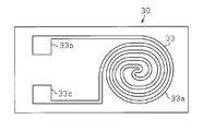
- the conductive layer 33 may be patterned in a spiral shape as shown in FIG. 15 as a modification of the pattern shown in FIG. As described above, when the conductive layer 33 is patterned in a spiral shape, the conductive layer 33 is cut or changed in resistance to omnidirectional cracks or cracks in the glass plate 13.
- the sensor film 30 in FIG. 2, the sensor film 30 in FIG. 14, and the sensor film 30 in FIG. 15 are selectively used according to the following specifications.
- the sensor film 30 in which the thin line portion 33 a extends in a straight line is suitable when the extending direction of the crack due to the breakage of the glass plate 13 can be specified in advance.
- the sensor film 30 in which the pattern of the thin line portion 33 a is folded back in a comb shape is suitable for a case where the occurrence location of the crack due to the breakage of the glass plate 13 and the direction in which the crack extends can be specified in advance. Yes. It is also effective when it is necessary to measure the degree of cracks.
- the sensor film 30 shown in FIG. 15 in which the thin wire portion 33a has a spiral shape can be specified in advance where a crack is generated due to breakage of the glass plate 15, but is effective when the direction in which the crack extends is unknown.
- FIG. 17 shows a longitudinal section taken along line 17-17 in FIG.
- FIG. 17 shows the sensor film 30 after being attached to the glass plate 13
- FIG. 18 shows the sensor film 30 before being attached to the glass plate 13.
- an insulating layer (resin layer) 38 is formed on the adhesive layer 31, and an insulating layer 37 is patterned on the upper surface of the insulating layer 38. If it demonstrates in FIG. 16, the thin wire
- the insulating layer 37 is patterned so as to extend radially from the center of the spiral toward the outside in the radial direction of the spiral at predetermined angles.
- a step is formed in the conductive layer 33 by an insulating layer (resin layer) 37. That is, the conductive layer 33 is spirally patterned on the insulating layer 38 and the insulating layer 37.
- An insulating layer (resin layer) 39 is formed on the conductive layer 33.
- the sensor film 30 in this embodiment is formed on a plastic film 40 in a state before being attached to the glass plate 13.
- An insulating layer 39 is formed on the plastic film 40, and the conductive layer 33 is patterned on the insulating layer 39.
- the conductive layer 33 is patterned so as to straddle the insulating layer 37.
- An insulating layer 38 is formed on the insulating layer 39, and an adhesive layer 31 is formed on the insulating layer 38.
- the sensor film 30 shown in FIG. 18 is attached to the glass plate 13 of the vehicle as shown in FIG. That is, the adhesive layer 31 of the sensor film 30 is brought into contact with one surface (glass surface) of the glass plate 13, and the sensor film 30 is attached to the glass plate 13 by the adhesive layer 31. Thereafter, when the plastic film 40 is peeled off from the sensor film 30, the sensor film 30 is attached to the glass plate 13. At this time, as shown in FIG. 16, the insulating layer 37 is provided radially at predetermined angles from the center of the spiral toward the outside in the radial direction of the spiral.
- the sensor film 30 has the insulating layer 37 formed between the adhesive layer 31 and the conductive layer 33, and the insulating layer 37 is formed of the conductive layer 33. Patterning is performed so as to extend in a direction orthogonal to the extending direction. Thereby, since the distortion of the conductive layer 33 accompanying the breakage of the glass plate 13 is amplified by the insulating layer 37, the presence or absence of breakage of the glass plate 13 can be detected with high sensitivity.
- the conductive layer 33 has irregularities 75 on the surface thereof.
- the irregularities 75 on the surface of the conductive layer 33, the distortion of the conductive layer 33 accompanying the breakage of the glass plate 13 is amplified, and the breakage of the glass plate 13 can be detected with high sensitivity.
- the conductive layer 33 may be formed as a two-layer structure as shown in FIG.
- the conductive layer Concavities and convexities 75 may be formed on the surface 33.
- an insulating layer 37 for generating irregularities 75 on the surface of the conductive layer 33 may be formed. At this time, the insulating layer 37 is provided in parallel with a predetermined distance.
- an insulating layer 37 may also be formed, which extends in the direction of the arrow X in FIG. 14 and causes unevenness 75 on the surface of the conductive layer 33.
- the sensor film 30 of this embodiment has a structure shown in FIG. FIG. 21 is a cross-sectional view of the sensor film 30, and FIG. 22 is a plan view of the sensor film 30. 21 and 22 show a state after the sensor film 30 is attached to the glass plate 13.
- the sensor film 30 in the present embodiment includes a design layer 80 on the adhesive layer 31.
- the design layer 80 is formed by printing.
- the insulating layer 32 is formed on the design layer 80, the conductive layer 33 is patterned on the insulating layer 32, and the insulating layer 34 is formed on the conductive layer 33 and the insulating layer 32.
- a design printed matter is drawn on the design layer 80 of FIG. 21 as shown in FIG. In FIG. 22, a square frame and a character “Sensor is operating” are printed in the frame. Therefore, when the triangular window 12 at the rear of the vehicle 11 in FIG. 1 is viewed from outside the vehicle, the conductive layer 33 can be shielded by the design layer 80 as shown in FIG. Because “inside” can be seen, crime can be prevented.
- the design layer 80 only needs to be patterned with characters, pictures, designs, patterns, and the like, and thereby, it is possible to add a function of improving the design property and improving the crime prevention effect by visual observation.
- a seventh embodiment embodying the present invention will be described focusing on differences from the above embodiments.
- the conductive layer 33 is formed using printing ink made of silver particles and / or carbon particles dispersed in the resin in the manufacturing process of the sensor film 30, but instead, this embodiment Then, it is as follows. That is, the conductive layer 33 is formed using a printing ink containing at least organometallic particles. It is preferable to use organic silver particles as the organic metal particles. Specifically, for example, from metal oxide particles for any one metal selected from Ag, Au, Pt, Ni, Cu, Pd and Al, and Ag, Au, Pt, Ni, Cu, Pd and Al. The conductive layer 33 is formed using a printing ink containing organometallic particles for any one of the selected metals.
- the conductive layer 33 is formed using a printing ink containing thermally reactive silver oxide particles and organic silver particles. Thereby, the metal particles are electrically connected by direct welding to form the conductive layer 33.
- the metal particles have a particle size of about several nm to several tens of ⁇ m.
- a normal conductive ink is a thermosetting conductive ink in which silver particles are dispersed in a resin.
- the thermosetting conductive ink after heating the applied ink, the metal particles are dispersed in the resin as the binder as shown in FIG. 33 is formed.
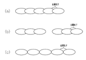
- the heat-reactive conductive ink is not a metal at the time of application, but becomes a metal when baked and has a brittle property. That is, after heating the applied ink, the metal particles are welded together by heat as shown in FIG. 24A, and the metal particles are connected even in the absence of resin. That is, the conductive layer 33 is formed by welding the metal particles together by heat.
- the conduction state of the electrical path of the window glass breakage sensor 20 is as follows.
- the resistance value of the conductive layer 33 has a predetermined value (for example, a resistance value “10”). .
- a predetermined value for example, a resistance value “10”.
- the conductive layer 33 is formed using a heat-reactive conductive ink. Even in this case, the resistance value of the conductive layer 33 becomes infinite.
- the resistance value of the conductive layer 33 is a predetermined value, for example, the resistance value.
- the resistance value of the conductive layer 33 is infinite.
- the resistance value of the conductive layer 33 is a predetermined value, for example, a resistance value.
- the resistance value of the conductive layer 33 is infinite.
- the resistance value of the conductive layer 33 is a predetermined value, for example, resistance
- the resistance value of the conductive layer 33 becomes a predetermined value, for example, the resistance value “15”.
- the conductive layer 33 when the conductive layer 33 is formed using a normal conductive ink (thermosetting conductive ink), the conductive layer 33 is easily stretched due to breakage of the glass plate 13, and the conductive layer 33 due to breakage of the glass plate 13. The resistance value changes continuously.
- the conductive layer 33 when the conductive layer 33 is formed using a heat-reactive conductive ink, the conductive layer 33 is easily cut due to breakage of the glass plate 13, and the resistance value of the conductive layer 33 depends on whether the glass plate 13 is broken or not. It changes binary.
- the conductive layer 33 is formed using normal conductive ink (thermosetting type conductive ink), a circuit for measuring a change in the resistance value of the conductive layer 33 is necessary, and the configuration of the circuit is complicated. Invite.
- the conductive layer 33 is formed using the heat-reactive conductive ink, it is only necessary to monitor the binarized resistance value in the conductive layer 33, thereby simplifying the circuit configuration. Can do.
- the window glass breakage sensor 20 (sensor film 30) may be of a type in which the adhesive layer 31 and the conductive layer 33 are laminated and printed on the glass plate 13 and attached to the glass plate 13 directly.
- the glass plate 13 may be laminated glass or tempered glass.
- the resistance value of the conductive layer 33 is likely to change due to distortion caused by breakage of the window glass.
- the property that the conductive layer 33 is cut by a crack caused by breakage of the window glass and the resistance value is theoretically infinite is used.
- the present invention may be applied to residential windows instead of automobile windows.
- SYMBOLS 12 Triangular window, 13 ... Glass plate, 20 ... Window glass break sensor, 30 ... Sensor film, 31 ... Adhesive layer, 32 ... Insulating layer, 33 ... Conductive layer, 33a ... Fine wire part, 32b ... Electrode, 33c ... Electrode, 34 ... insulating layer, 37 ... insulating layer, 40 ... plastic film, 60 ... determination circuit, 75 ... unevenness.
Landscapes
- Physics & Mathematics (AREA)
- General Physics & Mathematics (AREA)
- Burglar Alarm Systems (AREA)
- Investigating Or Analyzing Materials By The Use Of Electric Means (AREA)
Abstract
導電層と接着層と検出部とを備える窓ガラス破損センサが開示される。導電層は、窓に適用されるガラス板の表面上に配置される。導電層は、印刷によりパターニングされる。接着層は、前記導電層を前記ガラス板に貼り付ける。検出部は、前記導電層の切断または抵抗変化により前記ガラス板の破損を検出する。
Description
本発明は、窓ガラス破損センサ、窓ガラス破損センサフィルム、及び窓ガラス破損センサフィルムの製造方法に関する。
特許文献1には、被貼着体の美観を維持しつつ、種々の大きさの被貼着体に対して適用できる導体布線フィルムが開示されている。特許文献1の導体布線フィルムは、被貼着体の破損の有無を検知することができるとともに、被貼着体の霜取り及び曇り止めを行なうことができる。具体的には、導体布線フィルムは、樹脂製フィルムと導体とを具備する。樹脂製フィルムは、その主面上に接着剤層を有する。導体は、複数の直線部分及び湾曲部分を有し、該直線部分及び湾曲部分は接着剤層内に配置されている。導体の直線部分は互いに略平行に配置され、湾曲部分及び直線部分は全体として蛇行するように互いに繋がっている。直線状に配列する2つの湾曲部分列のうちいずれか一つの湾曲部分列における各湾曲部分には接続端子が接続されている。特許文献1には、導体の外径は10~100μmであることが好ましいと記載されている。
ところが、被貼着体、特にはガラスが破損した場合でも、破損したガラスが散らばらない限りガラスの破損が検出されない。つまり、ガラスの破損を検出するための前記導体は、直径10μm以上の均一な密度を持つ金属線であって、比較的よく伸びる性質を有する。そのため、ガラスに微小なクラックが生じても導体は断線しないためにガラスの破損を検知できない。言い換えると、上記特許文献1の導体布線フィルムは、ガラス破損センサとしては低感度である。検知感度を向上させるためには、導体布線フィルムをガラスの全面に亘って設ける必要がある。また、上記特許文献1の導体布線フィルムは、前記導体(金属線)を接着剤層内に配置する必要があるため、導体布線フィルムの生産コストがアップしてしまう。
本発明の目的は、確実にガラスの破損を検出することが可能となる窓ガラス破損センサ、窓ガラス破損センサフィルム、及び窓ガラス破損センサフィルムの製造方法を提供することにある。
上記目的を達成するために、本発明の第1の態様に従い、導電層と接着層と検出部とを備える窓ガラス破損センサが提供される。導電層は、窓に適用されるガラス板の表面上に配置される。導電層は、印刷によりパターニングされる。接着層は、前記導電層を前記ガラス板に貼り付ける。検出部は、前記導電層の切断または抵抗変化により前記ガラス板の破損を検出する。
上記目的を達成するために、本発明の第2の態様に従い、窓のガラス板に貼り付けられる窓ガラス破損センサフィルムが提供される。センサフィルムは、ベースフィルムと導電層と接着層とを備える。ベースフィルムは、印刷物を支持する。導電層は、前記ベースフィルム上に配置される。導電層は、印刷によりパターニングされる。導電層は、自身の切断または抵抗変化により前記ガラス板の破損を検出する。接着層は、前記ベースフィルム上に配置される。接着層は、印刷により形成される。接着層は、前記導電層を前記ガラス板に貼り付ける。
上記目的を達成するために、本発明の第3の態様に従い、窓ガラス破損センサフィルムの製造方法が提供される。該方法は、印刷物支持用ベースフィルムを準備する工程と、前記印刷物支持用ベースフィルム上に、自身の切断または抵抗変化により窓のガラス板の破損を検出するための導電層を印刷にてパターニングする工程と、前記導電層上に印刷にて接着層を形成する工程とを含む。
以下、本発明を具体化した第1の実施形態を図面に従って説明する。
図1(a)に示すように、車両11の後部における左右両側(左側のみ図示)には、自動車用窓としての三角窓12が設けられている。これら三角窓12は開閉不能な窓である。また、三角窓12のガラス板13は、その一部が破損した場合に全体的にひび割れが生じるように形成された窓ガラスである。ガラス板13は、強化ガラスである。
図1(a)に示すように、車両11の後部における左右両側(左側のみ図示)には、自動車用窓としての三角窓12が設けられている。これら三角窓12は開閉不能な窓である。また、三角窓12のガラス板13は、その一部が破損した場合に全体的にひび割れが生じるように形成された窓ガラスである。ガラス板13は、強化ガラスである。
図1(b)は、図1(a)の1b-1b線に沿った三角窓12付近の部分の断面図である。図1(b)に示すように、三角窓12のガラス板13は、該ガラス板13の周縁部において接着剤(ガラス接着剤)14を介して車体15に固着されている。なお、ガラス板13の厚さは3.1mm~5.0mm程度である。
図1(b)に示すように、ガラス板13の周縁部であって接着剤14よりも内側の部位には、窓ガラス破損センサ20の構成要素の一部であるセンサフィルム30が固着されている。窓ガラス破損センサ20は、自動車用窓のガラス板13の破損を検出するセンサである。フィルム30は、車両11の内装16によって覆われている。
以下、窓ガラス破損センサ20について、詳しく説明する。
図2は、センサフィルム30の平面及び断面を示す。図3は、窓ガラス破損センサ20の電気的構成図である。図4は、図2の4-4線での断面図である。図5の(a)~(e)はセンサフィルム30の製造方法を示す断面図である。
図2は、センサフィルム30の平面及び断面を示す。図3は、窓ガラス破損センサ20の電気的構成図である。図4は、図2の4-4線での断面図である。図5の(a)~(e)はセンサフィルム30の製造方法を示す断面図である。
図1(b)に示すように、窓ガラス破損センサ20は、センサフィルム30と判定回路60と警報器70を備えている。
センサフィルム30は、図2に示すように、平面構造としては長方形状をなしている。また、センサフィルム30は、図2及び図4に示すように、断面構造としては、接着層31と絶縁層32と導電層33と絶縁層34とを含む積層体である。絶縁層32,34は樹脂で形成されている。絶縁層32がベース部材として機能し、絶縁層34が表面保護膜として機能する。
センサフィルム30は、図2に示すように、平面構造としては長方形状をなしている。また、センサフィルム30は、図2及び図4に示すように、断面構造としては、接着層31と絶縁層32と導電層33と絶縁層34とを含む積層体である。絶縁層32,34は樹脂で形成されている。絶縁層32がベース部材として機能し、絶縁層34が表面保護膜として機能する。
導電層33は、1本の細線部33aと該細線部33aの両端に形成された電極33b,33cとを有する。細線部33aは、ガラス板13上に接着層31及び絶縁層32を介して配置されている。細線部33aは、印刷により線状に延びるようにパターニングされている。つまり、薄いセンサフィルム30はその内部(積層した複数のシート材の内部)において、印刷にてパターニングされた、細線部33aを有する導電層33を有している。細線部33aは、図2においてガラス板13の破損時に発生する割れが延びる方向またはクラックが延びる方向Xに対して交差するように(好ましくは実質的に直交する方向に)延設され、かつ複数回折り返したパターンとなっている。細線部33aの線幅は200μm程度である。
細線部33aは微細パターンなので断線しやすい。細線部33aの両端に形成された前記電極33b,33cは、細線部33aよりも幅広である。電極33b,33c上において絶縁層34には開口部34a,34bが形成され、開口部34a,34bを通して電極33b,33cが露出している。この開口部34a,34bが電極取り出し部となっている。接着層31により導電層33がガラス板13に貼り付けられている。
図2に示すセンサフィルム30が、図1(b)に示すようにガラス板13に貼り付けられて、これにより、ガラス板13上に電極33b,33cを有する導電層33が形成されている。図2の電極33b,33cのいずれか一方には、図1(b)に示すようにコネクタCを介してワイヤハーネス50の一端が接続され、ワイヤハーネス50の他端には判定回路60が接続されている。ガラス板13が割れると、微小なクラックにより、センサフィルム30の導電層33が切断されるか、または導電層33の抵抗が変化する。この導電層33の切断または抵抗変化によりガラス板13の破損が検出されるようになっている。
このように、センサフィルム30がガラス板13に貼り付けられているので、ガラス板13上に導電層33を直接印刷する必要がなくなるためコストダウンを図ることができる。また、センサフィルム30は、導電層33の無いガラス板13に対し後付けで取付けることができる。また、センサフィルム30は、細線よりなる導電層33を備えているので、ガラス板13が完全に粉砕しなくてもガラス板13の破損を検知可能となる。
図3において、導電層33における第1の端子30aは接地されている。導電層33における第2の端子30bは判定回路60の接続端子60aと電気的に接続されている。判定回路60(検出部)はマイコン61とトランジスタ62と抵抗63,64とを備えている。マイコン61の入力ポートは抵抗64を介して判定回路60の接続端子60aと接続されている。トランジスタ(npnトランジスタ)62は、電源端子+Bと接続されるコレクタと、抵抗63を介して接続端子60aと接続されるエミッタとを有する。トランジスタ62のベースはマイコン61の出力ポートと接続されている。また、マイコン61には警報器70が接続されている。
次に、図5及び図6を用いてセンサフィルム30の製造方法、及びガラス板13への取付方法について説明する。
まず、図5(a)に示すように、印刷物に対する支持体として機能するプラスチックフィルム40を用意する。印刷物を支持するためのベースフィルムとしてのプラスチックフィルム40は、センサフィルム30と同じ形状及び寸法である。プラスチックフィルム40は、ポリエチレンテレフタレート(PET)、ポリエチレンナフタレート(PEN)、アクリル、ポリカーボネート(PC)、ポリイミド(PI)、液晶ポリマー(LCP)、及びポリアリレート(PAR)から選ばれるいずれか1種の樹脂を用いて形成されている。特に、ポリイミド(PI)、液晶ポリマー(LCP)、及びポリアリレート(PAR)が、耐熱性という観点から好ましい。
まず、図5(a)に示すように、印刷物に対する支持体として機能するプラスチックフィルム40を用意する。印刷物を支持するためのベースフィルムとしてのプラスチックフィルム40は、センサフィルム30と同じ形状及び寸法である。プラスチックフィルム40は、ポリエチレンテレフタレート(PET)、ポリエチレンナフタレート(PEN)、アクリル、ポリカーボネート(PC)、ポリイミド(PI)、液晶ポリマー(LCP)、及びポリアリレート(PAR)から選ばれるいずれか1種の樹脂を用いて形成されている。特に、ポリイミド(PI)、液晶ポリマー(LCP)、及びポリアリレート(PAR)が、耐熱性という観点から好ましい。
そして、図5(b)に示すように、プラスチックフィルム40の上にスクリーン印刷にて絶縁層34を形成する。その後、絶縁層34を加熱する。
さらに、図5(c)に示すように、絶縁層34の上にスクリーン印刷にて導電層33をパターニングする。その後、導電層33を加熱する。
さらに、図5(c)に示すように、絶縁層34の上にスクリーン印刷にて導電層33をパターニングする。その後、導電層33を加熱する。
導電層33のパターニング工程において、導電層33を、熱硬化型のポリエステル系、ウレタン系、ゴム系、ポリイミド系、エポキシ系、及びフェノール系の樹脂から選ばれるいずれか1種の系の樹脂中に分散された導電性粒子(たとえば、銀粒子)からなる印刷インクを使用して形成する。つまり、導電層33は、バインダーとしての樹脂によって互いに電気的に接続された多数の導電性粒子を含む。
なお、導電性粒子としては、銀粒子に代わり、カーボン粒子でもよいし、また、銅(Cu)粒子、ニッケル(Ni)粒子、パラジウム(Pd)粒子や、さらに合金の粒子等、各種の金属粒子を使用し得る。あるいは、銀粒子及びカーボン粒子の両方を含む印刷インクを使用して導電層33を形成してもよい。
引き続き、図5(d)に示すように、絶縁層34の上にスクリーン印刷にて導電層33を覆うように絶縁層32を形成する。その後、絶縁層32を加熱する。
そして、図5(e)に示すように、絶縁層32の上にスクリーン印刷にて接着層31を形成する。その後、接着層31を加熱する。
そして、図5(e)に示すように、絶縁層32の上にスクリーン印刷にて接着層31を形成する。その後、接着層31を加熱する。
これにより、センサフィルム30が製造される。
センサフィルム30は、導電層33とプラスチックフィルム(ベースフィルム)40との間に絶縁層34を有する。当該絶縁層34は、熱硬化型または紫外線硬化型のポリエステル系印刷インク、アクリル系印刷インク、アクリルウレタン系印刷インク、ウレタン系印刷インク、及びポリイミド系印刷インクから選ばれるいずれか1種の印刷インクを使用して形成される。センサフィルム30は、接着層31と導電層33との間に絶縁層32を有する。当該絶縁層32は、熱硬化型または紫外線硬化型のポリエステル系印刷インク、アクリル系印刷インク、アクリルウレタン系印刷インク、ウレタン系印刷インク、及びポリイミド系印刷インクから選ばれるいずれか1種の印刷インクを使用して形成される。
センサフィルム30は、導電層33とプラスチックフィルム(ベースフィルム)40との間に絶縁層34を有する。当該絶縁層34は、熱硬化型または紫外線硬化型のポリエステル系印刷インク、アクリル系印刷インク、アクリルウレタン系印刷インク、ウレタン系印刷インク、及びポリイミド系印刷インクから選ばれるいずれか1種の印刷インクを使用して形成される。センサフィルム30は、接着層31と導電層33との間に絶縁層32を有する。当該絶縁層32は、熱硬化型または紫外線硬化型のポリエステル系印刷インク、アクリル系印刷インク、アクリルウレタン系印刷インク、ウレタン系印刷インク、及びポリイミド系印刷インクから選ばれるいずれか1種の印刷インクを使用して形成される。
導電層33において導電性粒子同士を電気的につなぐバインダーの材料としては、ポリエステル系、アクリル系、アクリルウレタン系、ウレタン系、ポリイミド系の樹脂を挙げることができる。上記樹脂以外にも、導電層33におけるバインダーは、絶縁性を有するという観点から次の材料を使用することができる。即ち、導電層33におけるバインダーは、蒸発乾燥型バインダーとしては、アクリル樹脂、共重合ポリエステル、ポリウレタン、塩ビ酢ビ共重合体を使用し得る。また、導電層33におけるバインダーは、熱硬化型バインダーとしては、エポキシ樹脂、フェノール樹脂、共重合ポリエステル、ポリウレタン、塩ビ酢ビ共重合体を使用し得る。さらに、導電層33におけるバインダーは、UV硬化型インダーとしては、アクリル樹脂、アクリルウレタン樹脂を使用し得る。さらにまた、導電層33におけるバインダーとしては、塩ビ系、エポキシ系、フェノール系、オレフィン系、シリコーン系の樹脂を使用し得る。要は、導電層33におけるバインダーとしては、熱可塑性樹脂や熱硬化性樹脂、UV硬化樹脂等を使用することができる。
図5(e)において、プラスチックフィルム40の厚さは50~数100μm程度であり、接着層31の厚さは数μm程度(例えば6μm)であり、絶縁層32の厚さは数μm程度(例えば3μm)であり、導電層33の厚さは数μm程度(例えば3μm)であり、絶縁層34の厚さは数μm程度(例えば3μm)である。
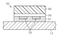
このセンサフィルム30を車両のガラス板13に装着する際には、図6(a)に示すように、ガラス板13の一方の面(ガラス面)に対して、センサフィルム30の接着層31を接触させて接着層31によりガラス板13にセンサフィルム30を貼り付ける。
接着層31として熱硬化型接着剤を用いることができる。他にも、接着層31として両面テープを用いてもよく、この両面テープの粘着剤として、アクリル系ノンキャリア粘着剤やゴム系粘着剤やシリコーン系粘着剤やビニール系粘着剤を用いるとよい。
その後、プラスチックフィルム40を絶縁層34から剥がすと、図6(b)に示すように、センサフィルム30がガラス板13に装着される。
このようにして、センサフィルム30は、ガラス板13に貼り付ける際にプラスチックフィルム40から剥離されることで印刷膜のみが残留する転写タイプである。
このようにして、センサフィルム30は、ガラス板13に貼り付ける際にプラスチックフィルム40から剥離されることで印刷膜のみが残留する転写タイプである。
次に、このように構成した窓ガラス破損センサ20の動作を説明する。
ガラス板13の一部が破損すると、ガラス板13全体にひび(クラック)が入る。この状態を図7に示す。図7は図2の7-7線に対応する部位の断面図である。
ガラス板13の一部が破損すると、ガラス板13全体にひび(クラック)が入る。この状態を図7に示す。図7は図2の7-7線に対応する部位の断面図である。
図7は、導電層33の延設方向と直交する方向に延びるクラックにより切断された導電層33の断面図を示す。たとえ、工具を用いてガラス板13を振動させることなく破損させても、センサフィルム30の貼着部ではひび割れによって細線よりなる導電層33が切断される、もしくは、クラックの大きさにより導電層33の一部領域にクラックが入る。この場合には、導電層33の抵抗が大きくなる。導電層33が切断された場合は導電層33の抵抗値が無限大になり、導電層33の一部にクラックが入った場合には導電層33の抵抗値が所定量だけ増大する。
図3の判定回路60のマイコン61は一定周期で出力ポートをHレベルにしてトランジスタ62をオンしている。そして、マイコン61は入力ポートの電位のレベルが予め定めた電位よりも高いか否か判定する。センサフィルム30の導電層33が切断していない、もしくは、導電層33の一部領域にクラックが入っていない場合、抵抗値は増大せず、マイコン入力ポートの電位レベルは常にグランドレベルとなる。マイコン61はトランジスタ62をオンしたときに入力ポートの電位レベルがグランドレベルであると、ガラス板13が破損しておらず正常であると判定する。
一方、ガラス板13が破損すると、導電層33が切断する、もしくは、導電層33の一部領域にクラックが生じ、抵抗値が大きくなる。マイコン61は、トランジスタ62をオンしたときに入力ポートの電位レベルがグランドレベルでないと、ガラス板13が破損していると判定する。そして、マイコン61は警報器70にて警報音や警報ランプによりガラス板13が破損している(異常が発生している)旨を外部に報知する。
本実施形態は、以下の利点を有する。
(1)図4に示すように、窓ガラス破損センサ20は、ガラス板13の表面において印刷により線状に延びるようにパターニングされた導電層33と、導電層33をガラス板13に貼り付けるための接着層31とを備える。窓ガラス破損センサ20は、導電層33の抵抗の変化によりガラス板13の破損を検出する。図5の(e)に示すように、センサフィルム30は、プラスチックフィルム40上において印刷により線状に延びるようにパターニングされた導電層33と、プラスチックフィルム40上において印刷により形成された、導電層33をガラス板13に貼り付けるための接着層31とを備えている。このようなセンサフィルム30の製造方法は、図5に示すように、ベースフィルムとしてのプラスチックフィルム40上に印刷にて線状に延びるように導電層33をパターニングする導電層パターニング工程と、導電層33上に印刷にて接着層31を形成する接着層形成工程とを有する。
(1)図4に示すように、窓ガラス破損センサ20は、ガラス板13の表面において印刷により線状に延びるようにパターニングされた導電層33と、導電層33をガラス板13に貼り付けるための接着層31とを備える。窓ガラス破損センサ20は、導電層33の抵抗の変化によりガラス板13の破損を検出する。図5の(e)に示すように、センサフィルム30は、プラスチックフィルム40上において印刷により線状に延びるようにパターニングされた導電層33と、プラスチックフィルム40上において印刷により形成された、導電層33をガラス板13に貼り付けるための接着層31とを備えている。このようなセンサフィルム30の製造方法は、図5に示すように、ベースフィルムとしてのプラスチックフィルム40上に印刷にて線状に延びるように導電層33をパターニングする導電層パターニング工程と、導電層33上に印刷にて接着層31を形成する接着層形成工程とを有する。
よって、導体は布線によらずに印刷により形成されており、確実にガラス板13の破損を検出することが可能となる。
(2)図2に示すように、導電層33は、ガラス板13の破損時に発生する割れの方向またはクラックの延びる方向に対して実質的に直交する方向Xに延設されているので、ガラス板13の破損を検出する上で好ましい。
(2)図2に示すように、導電層33は、ガラス板13の破損時に発生する割れの方向またはクラックの延びる方向に対して実質的に直交する方向Xに延設されているので、ガラス板13の破損を検出する上で好ましい。
(3)図6(a)及び(b)に示すように、プラスチックフィルム40は、センサフィルム30をガラス板13に貼り付け後においてセンサフィルム30から剥離されるので、センサフィルム30は、高感度なセンサとして機能し得る。
センサフィルム30の接着層31として、センサフィルム30をガラス板13に貼り付ける際にセンサフィルム30をガラス板13に圧接して接着する感圧型接着剤を用いてもよい。また、接着層31として、センサフィルム30をガラス板13に貼り付ける際にセンサフィルム30及びガラス板13の少なくとも一方を加熱しかつセンサフィルム30をガラス板13に圧接することで接着する熱圧着型接着剤を用いてもよい。さらに、接着層31として、センサフィルム30をガラス板13に貼り付ける際にセンサフィルム30及びガラス板13の少なくとも一方を誘導加熱することでセンサフィルム30をガラス板13に接着する誘導加熱型接着剤を用いてもよい。さらにまた、接着層31として、センサフィルム30をガラス板13に貼り付ける際にセンサフィルム30及びガラス板13の少なくとも一方に活性エネルギー線(電子線、X線、紫外線、可視光線、赤外線など)を照射することで硬化してセンサフィルム30をガラス板13に接着する接着剤(UV接着剤等)を用いてもよい。
次に、本実施形態の変形例を説明する。図6(b)においては図6(a)のプラスチックフィルム40をセンサフィルム30から剥がしたが、図8に示すように、図6(a)のプラスチックフィルム40を剥がすことなくセンサフィルム30をそのまま使用してもよい。
次に、本発明を具体化した第2の実施形態を、第1の実施形態との相違点を中心に説明する。
本実施形態の窓ガラス破損センサ20のセンサフィルム30は、図9及び図10に示す構造を有している。
本実施形態の窓ガラス破損センサ20のセンサフィルム30は、図9及び図10に示す構造を有している。
図9に示すように、ガラス板13に装着前の状態において、本実施形態におけるセンサフィルム30では、プラスチックフィルム40上に絶縁層34が形成されている。絶縁層34上には導電層33がパターニングされ、導電層33上及び絶縁層34上には接着層31が形成されている。
この図9に示すセンサフィルム30が、図10に示すように、車両のガラス板13に装着される。つまり、ガラス板13の一方の面(ガラス面)に対して、センサフィルム30の接着層31を接触させて接着層31によりガラス板13にセンサフィルム30を貼り付ける。その後、プラスチックフィルム40をセンサフィルム30から剥がすと、センサフィルム30がガラス板13に装着される。
次に、本実施形態の変形例を説明する。図10においては図9のプラスチックフィルム40をセンサフィルム30から剥がしたが、図11に示すように、図9のプラスチックフィルム40を剥がすことなくセンサフィルム30をそのまま使用してもよい。
次に、本発明を具体化した第3の実施形態を、第1の実施形態との相違点を中心に説明する。
本実施形態の窓ガラス破損センサ20のセンサフィルム30は、図12及び図13に示す構造を有している。
本実施形態の窓ガラス破損センサ20のセンサフィルム30は、図12及び図13に示す構造を有している。
図12に示すように、ガラス板13に装着前の状態において、本実施形態におけるセンサフィルム30はプラスチックフィルム40の第1の面上に絶縁層34が形成されている。絶縁層34上には導電層33がパターニングされ、導電層33及び絶縁層34上には絶縁層32が形成されている。一方、プラスチックフィルム40の第2の面上には接着層36が形成されている。
この図12に示すセンサフィルム30が、図13に示すように、車両のガラス板13に装着される。つまり、ガラス板13の一方の面(ガラス面)に対して、センサフィルム30の接着層36を接触させて接着層36によりガラス板13にセンサフィルム30を貼り付ける。これにより、センサフィルム30がガラス板13に装着される。
ここで、図5(e)のセンサフィルム30と、図9のセンサフィルム30と、図12のセンサフィルム30とは、次のような仕様に合わせて使い分ける。
図5(e)に示す絶縁層32,34を具備するセンサフィルム30は、高感度であるとともにガラス板13に装着しやすい。ここで、図4に示すようにプラスチックフィルム40をセンサフィルム30から剥離して取り除くと、窓ガラス破損センサ20を高感度タイプの窓ガラス破損センサとして使用できる。一方、図8に示すように、プラスチックフィルム40をセンサフィルム30から剥離せずに残すと窓ガラス破損センサ20を低感度タイプの窓ガラス破損センサとして使用できる。
図5(e)に示す絶縁層32,34を具備するセンサフィルム30は、高感度であるとともにガラス板13に装着しやすい。ここで、図4に示すようにプラスチックフィルム40をセンサフィルム30から剥離して取り除くと、窓ガラス破損センサ20を高感度タイプの窓ガラス破損センサとして使用できる。一方、図8に示すように、プラスチックフィルム40をセンサフィルム30から剥離せずに残すと窓ガラス破損センサ20を低感度タイプの窓ガラス破損センサとして使用できる。
図9に示すセンサフィルム30は最高感度であるが、センサフィルム30がガラス板13に装着しにくい。ここで、図10に示すようにプラスチックフィルム40をセンサフィルム30から剥離して取り除くと窓ガラス破損センサ20を高感度タイプとして使用でき、図11に示すようにプラスチックフィルム40をセンサフィルム30から剥離せずに残すと低感度タイプとして使用できる。
図12に示すセンサフィルム30は、厚いプラスチックフィルム40によりガラス板13で発生したクラックも導電層33に到達しにくくなる。従って、図12に示すセンサフィルム30は、低感度である。一方、図13に示すように、ガラス板13に極めて容易に装着することができる。
なお、絶縁層32,34や接着層36の膜厚を調整することによってもセンサフィルム30のセンサ感度を調整することができる。
次に、本発明を具体化した第4の実施形態を、第1の実施形態との相違点を中心に説明する。
次に、本発明を具体化した第4の実施形態を、第1の実施形態との相違点を中心に説明する。
本実施形態の窓ガラス破損センサ20のセンサフィルム30は、図14に示す構造を有する。
図14において、導電層33はU字状にパターニングされ、その両端には細線部33aよりも幅広な電極33b,33cが形成されている。
図14において、導電層33はU字状にパターニングされ、その両端には細線部33aよりも幅広な電極33b,33cが形成されている。
導電層33は、図2に示すようなパターンに対する変形例として、図15に示すように、渦巻き状にパターニングしてもよい。このように、導電層33が渦巻き状にパターンニングされている場合、ガラス板13における全方向のクラックや割れに対して導電層33の切断や抵抗変化が生じる。
図2のセンサフィルム30と、図14のセンサフィルム30と、図15のセンサフィルム30とは、次のような仕様に合わせて使い分ける。
図14に示すように、細線部33aが一直線に延びているセンサフィルム30は、ガラス板13の破損によるクラックの延びる方向を予め特定できる場合に好適である。また、センサフィルム30をガラス板13の一辺と同程度の長さでガラス板13に貼り付けることができる場合に有効である。
図14に示すように、細線部33aが一直線に延びているセンサフィルム30は、ガラス板13の破損によるクラックの延びる方向を予め特定できる場合に好適である。また、センサフィルム30をガラス板13の一辺と同程度の長さでガラス板13に貼り付けることができる場合に有効である。
図2に示すように、細線部33aのパターンが櫛歯状に折り返されているセンサフィルム30は、ガラス板13の破損によるクラックの発生場所とクラックの延びる方向とが予め特定できる場合に向いている。また、クラックの度合いを測定する必要がある場合に有効である。
細線部33aが渦巻き状となっている図15に示すセンサフィルム30は、ガラス板15の破損によるクラックの発生場所を予め特定できるが、クラックの延びる方向が不明な場合に有効である。
次に、本発明を具体化した第5の実施形態を、第4の実施形態との相違点を中心に説明する。
本実施形態の窓ガラス破損センサ20は、図16に示す構造を有している。図16における17-17線での縦断面を図17に示す。図17はガラス板13に装着後のセンサフィルム30を示し、図18はガラス板13に装着前のセンサフィルム30を示す。
本実施形態の窓ガラス破損センサ20は、図16に示す構造を有している。図16における17-17線での縦断面を図17に示す。図17はガラス板13に装着後のセンサフィルム30を示し、図18はガラス板13に装着前のセンサフィルム30を示す。
図17において接着層31上には絶縁層(樹脂層)38が形成され、絶縁層38上面には絶縁層37がパターニングされている。図16で説明するならば、導電層33の細線部33aは渦巻き状にパターニングされている。絶縁層37は、その渦巻きの中心から該渦巻きの径方向外側に向かって所定角度ごとに放射状に延びるようにパターニングされている。図17に示すように、導電層33には、絶縁層(樹脂層)37により段差が形成される。つまり、導電層33は、絶縁層38及び絶縁層37上に渦巻き状にパターニングされている。また、導電層33上には絶縁層(樹脂層)39が形成されている。
図18に示すように、ガラス板13に装着前の状態において、本実施形態におけるセンサフィルム30はプラスチックフィルム40の上に形成されている。プラスチックフィルム40の上には絶縁層39が形成され、絶縁層39の上には導電層33がパターニングされている。導電層33は絶縁層37をまたぐようにパターニングされている。絶縁層39上には絶縁層38が形成され、その絶縁層38上には接着層31が形成されている。
この図18に示すセンサフィルム30が、図17に示すように、車両のガラス板13に装着される。つまり、ガラス板13の一方の面(ガラス面)に対して、センサフィルム30の接着層31を接触させて接着層31によりガラス板13にセンサフィルム30を貼り付ける。その後、プラスチックフィルム40をセンサフィルム30から剥がすと、センサフィルム30がガラス板13に装着される。このとき、絶縁層37は図16に示すように、前記渦巻きの中心から該渦巻きの径方向外側に向かって放射状に所定角度ごとに設けられている。
この絶縁層37の存在によりクラックによる導電層33の歪みが増幅され、同歪みが導電層33で検出される。
以上のごとく、図17及び図18に示すように、センサフィルム30は、接着層31と導電層33との間に形成される絶縁層37を有し、当該絶縁層37は、導電層33の延設方向と直交する方向に延びるようにパターニングされる。これにより、絶縁層37によってガラス板13の破損に伴う導電層33の歪みが増幅されるため高感度にガラス板13の破損の有無を検出することができる。
以上のごとく、図17及び図18に示すように、センサフィルム30は、接着層31と導電層33との間に形成される絶縁層37を有し、当該絶縁層37は、導電層33の延設方向と直交する方向に延びるようにパターニングされる。これにより、絶縁層37によってガラス板13の破損に伴う導電層33の歪みが増幅されるため高感度にガラス板13の破損の有無を検出することができる。
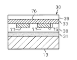
また、図17及び図18に示すように、導電層33は、その表面に凹凸75を有する。導電層33の表面に凹凸75を形成することにより、ガラス板13の破損に伴う導電層33の歪みが増幅されて高感度にガラス板13の破損を検出することができる。導電層33の表面に凹凸75を形成する別の構成として、図19に示すように、導電層33を二層の積層構造として形成するようにしてもよい。つまり、第1の導電層76の上の所定領域に第2の導電層77を積層することにより、両導電層76,77を含む二層構造の導電層33を形成することで、その導電層33の表面に凹凸75を形成してもよい。
次に、本実施形態の変形例を説明する。図2に示したセンサフィルム30について、図20に示すように、導電層33の表面に凹凸75を生じさせるための絶縁層37を形成してもよい。このとき、絶縁層37は平行に所定の距離だけ離間して設けられている。
なお、図14のセンサフィルム30においても同様に図14におけるX矢印方向に沿って延びる、導電層33の表面に凹凸75を生じさせるための絶縁層37を形成してもよい。
次に、本発明を具体化した第6の実施形態を、第1の実施形態との相違点を中心に説明する。
本実施形態のセンサフィルム30は、図21に示す構造を有する。図21はセンサフィルム30の断面図であり、図22はセンサフィルム30の平面図である。図21及び図22は、ガラス板13にセンサフィルム30を装着した後の状態を示す。
本実施形態のセンサフィルム30は、図21に示す構造を有する。図21はセンサフィルム30の断面図であり、図22はセンサフィルム30の平面図である。図21及び図22は、ガラス板13にセンサフィルム30を装着した後の状態を示す。
図21に示すように、本実施形態におけるセンサフィルム30は接着層31の上に意匠層80を備えている。意匠層80は印刷により形成されている。意匠層80の上に絶縁層32が形成され、絶縁層32の上に導電層33がパターニングされ、導電層33及び絶縁層32上に絶縁層34が形成されている。
図21の意匠層80には、図22に示すように意匠印刷物が描かれている。図22では、四角の枠と、その枠内に「センサ動作中」と記載された文字とが印刷されている。
よって、車外から図1における車両11の後部の三角窓12を見ると、図22に示すように意匠層80によって導電層33を遮蔽できるとともにガラス板13において四角枠内の文字である「センサ動作中」が見えるので、犯罪の予防を図ることができる。
よって、車外から図1における車両11の後部の三角窓12を見ると、図22に示すように意匠層80によって導電層33を遮蔽できるとともにガラス板13において四角枠内の文字である「センサ動作中」が見えるので、犯罪の予防を図ることができる。
意匠層80には、文字や絵や図柄や模様等がパターニングされていればよく、これにより意匠性の向上や目視による防犯効果向上の機能を付加することができる。
次に、本発明を具体化した第7の実施形態を、前記各実施形態との相違点を中心に説明する。
次に、本発明を具体化した第7の実施形態を、前記各実施形態との相違点を中心に説明する。
上記各実施形態ではセンサフィルム30の製造工程において樹脂の中に分散された銀粒子またはカーボン粒子もしくはその両方からなる印刷インクを使用して導電層33を形成したが、これに代わり、本実施形態では次のようにしている。即ち、導電層33を、少なくとも有機金属粒子を含む印刷インクを使用して形成する。有機金属粒子として有機銀粒子を用いるのが好ましい。具体的には、例えば、Ag、Au、Pt、Ni、Cu、Pd及びAlから選ばれるいずれか1種の金属についての酸化金属粒子と、Ag、Au、Pt、Ni、Cu、Pd及びAlから選ばれるいずれか1種の金属についての有機金属粒子とを含む印刷インクを使用して導電層33を形成する。より具体的には、熱反応型の酸化銀粒子と有機銀粒子とを含む印刷インクを使用して導電層33を形成する。これにより、金属粒子同士が直接溶着にて電気的に接続して導電層33が構成されている。前記金属粒子の粒径は数nm~数十μm程度である。
以下、通常の導電インクを用いた場合と、熱反応型の導電インクを用いた場合とを比較する。
通常の導電インクは、熱硬化型の導電インクであり、樹脂中に銀粒子が分散している。熱硬化型の導電インクでは、塗布されたインクを加熱した後においては、図23(a)に示すようにバインダーとしての樹脂中に金属粒子が分散しており、金属粒子同士の接触により導電層33が形成される。
通常の導電インクは、熱硬化型の導電インクであり、樹脂中に銀粒子が分散している。熱硬化型の導電インクでは、塗布されたインクを加熱した後においては、図23(a)に示すようにバインダーとしての樹脂中に金属粒子が分散しており、金属粒子同士の接触により導電層33が形成される。
これに対し、熱反応型の導電インクは、塗布時には金属ではないが焼付すると金属となり、脆い性質を有する。つまり、塗布されたインクを加熱した後においては、図24(a)に示すように金属粒子同士が熱によって溶着しており、金属粒子同士がたとえ樹脂のない状態でもつながっている。つまり、金属粒子同士が熱によって溶着することで導電層33が形成される。
よって、図25(b)に示すようにガラス板13が粉砕されたとき、及び、図25(c),(d),(e),(f)に示すようにガラス板13にクラックが発生した場合には、窓ガラス破損センサ20の電気経路の導通状態は以下のようになる。
(A);図25(b)に示すように、ガラス板13が複数の破片に別れるようにガラス板13が破損する場合においては、導電層33の細線部33aが破断する。このとき、通常の導電インク(熱硬化型導電インク)を使用して導電層33を形成した場合には、図23(b)に示すように金属粒子及びバインダー共に破断し、導電層33を含む窓ガラス破損センサ20の電気経路はオープン状態となる。一方、熱反応型の導電インクを使用して導電層33を形成した場合には、図24(b)に示すように金属粒子同士の連結が破断し、導電層33を含む窓ガラス破損センサ20の電気経路はオープン状態となる。
(B);図25(c)に示すように大きなクラックがガラス板13に発生した場合においてはガラス板13の表面でのクラックの幅が大きく導電層33の細線部33aが破断する。このとき、通常の導電インク(熱硬化型導電インク)を使用して導電層33を形成した場合には、図23(c)に示すように金属粒子及びバインダー共に破断し、導電層33を含む窓ガラス破損センサ20の電気経路はオープン状態となる。一方、熱反応型の導電インクを使用して導電層33を形成した場合には図24(b)に示すように金属粒子同士の連結が破断し、導電層33を含む窓ガラス破損センサ20の電気経路はオープン状態となる。
(C);図25(d)に示すように中程度のクラックがガラス板13に発生した場合においては、ガラス板13の表面でのクラック幅が中程度に大きく導電層33の細線部33aが破断する。このとき、通常の導電インク(熱硬化型導電インク)を使用して導電層33を形成した場合には図23(d)に示すようにバインダーは破断しないで金属粒子同士が離れ、導電層33は高抵抗化する。一方、熱反応型の導電インクを使用して導電層33を形成した場合には図24(b)に示すように金属粒子同士の連結が破断し、導電層33を含む窓ガラス破損センサ20の電気経路はオープン状態となる。
(D);図25(e)に示すように小さなクラックがガラス板13に発生した場合においては、ガラス板13の表面でのクラックの幅が小さく導電層33の一部までクラックが到達する。このとき、通常の導電インク(熱硬化型導電インク)を使用して導電層33を形成した場合には図23(e)に示すようにバインダーは破断しないで金属粒子の接触面積が減少し、導電層33は高抵抗化する。一方、熱反応型の導電インクを使用して導電層33を形成した場合には図24(b)に示すように金属粒子同士の連結が破断し、導電層33を含む窓ガラス破損センサ20の電気経路はオープン状態となる。
(E);図25(f)に示すように微小なクラックがガラス板13に発生した場合においてはガラス板13の表面でのクラックの幅が微小であり導電層33までクラックが到達していない。このとき、通常の熱硬化型導電インクを使用して導電層33を形成した場合には図23(f)に示すようにバインダーは破断しないで金属粒子同士の連結もほとんど影響を受けずに導電層33の抵抗値が僅かに変化する。一方、熱反応型の導電インクを使用して導電層33を形成した場合には図24(c)に示すように金属成分の延伸率内のため金属粒子同士の連結は破断せずに導電層33の抵抗値が変化する。
このようにして、図25(a)に示すようにガラス板13にセンサフィルム30を装着した当初においては、導電層33の抵抗値は所定値(例えば抵抗値「10」)を有している。上述の(A),(B)においては、通常の導電インク(熱硬化型導電インク)を使用して導電層33を形成した場合でも、熱反応型導電インクを使用して導電層33を形成した場合でも、導電層33の抵抗値は無限大となる。また、上述の(C)においては、通常の導電インク(熱硬化型導電インク)を使用して導電層33を形成した場合には、その導電層33の抵抗値は所定の値、例えば抵抗値「1000」を示し、熱反応型の導電インクを使用して導電層33を形成した場合には、その導電層33の抵抗値は無限大となる。さらに、上述の(D)においては、通常の導電インク(熱硬化型導電インク)を使用して導電層33を形成した場合には、その導電層33の抵抗値は所定の値、例えば抵抗値「100」を示し、熱反応型の導電インクを使用して導電層33を形成した場合には、その導電層33の抵抗値は無限大となる。さらには、上述の(E)においては、通常の導電インク(熱硬化型導電インク)を使用して導電層33を形成した場合には、その導電層33の抵抗値は所定の値、例えば抵抗値「20」を示し、熱反応型の導電インクを使用して導電層33を形成した場合には、その導電層33の抵抗値は所定の値、例えば抵抗値「15」となる。
このようにして、通常の導電インク(熱硬化型導電インク)を使用して導電層33を形成した場合、導電層33はガラス板13の破損により延伸しやすくガラス板13の破損によって導電層33の抵抗値が連続的に変化する。一方、熱反応型の導電インクを使用して導電層33を形成した場合、ガラス板13の破損により導電層33は切断しやすく、ガラス板13の破損の有無によってその導電層33の抵抗値が二値的に変化する。
よって、通常の導電インク(熱硬化型導電インク)を用いて導電層33を形成した場合、その導電層33の抵抗値の変化を測定する回路が必要であり、該回路の構成の複雑化を招く。これに対して、熱反応型導電インクを用いて導電層33を形成した場合、その導電層33における二値化された抵抗値をモニタするだけでよくそのための回路の構成の簡素化を図ることができる。
上記各実施形態は前記に限定されるものではなく、例えば、次のように具体化してもよい。
窓ガラス破損センサ20(センサフィルム30)は、ガラス板13に直接、接着層31及び導電層33を積層印刷してガラス板13に貼り付けるタイプであってもよい。
窓ガラス破損センサ20(センサフィルム30)は、ガラス板13に直接、接着層31及び導電層33を積層印刷してガラス板13に貼り付けるタイプであってもよい。
ガラス板13は合わせガラスでも強化ガラスでもよい。合わせガラスの場合には、窓ガラス破損による歪みで導電層33の抵抗値が変化しやすい。強化ガラスの場合には、窓ガラス破損によるクラックで導電層33が切断して抵抗値が理論上無限大になる性質を利用する。
本発明を自動車用窓に代わり住宅用窓に適用してもよい。
12…三角窓、13…ガラス板、20…窓ガラス破損センサ、30…センサフィルム、31…接着層、32…絶縁層、33…導電層、33a…細線部、32b…電極、33c…電極、34…絶縁層、37…絶縁層、40…プラスチックフィルム、60…判定回路、75…凹凸。
Claims (20)
- 窓に適用されるガラス板の表面上に配置される、印刷によりパターニングされた導電層と、
前記導電層を前記ガラス板に貼り付けるための接着層と、
前記導電層の切断または抵抗変化により前記ガラス板の破損を検出する検出部と
を備える、窓ガラス破損センサ。 - 前記導電層は、前記ガラス板の破損時に発生する割れの方向またはクラックの延びる方向に直交する方向に延設されている、請求項1に記載のセンサ。
- 前記導電層は、渦巻き状に延設されている、請求項1に記載のセンサ。
- 前記接着層と前記導電層との間に形成され、前記導電層の延設方向と直交する方向に延びるようにパターニングされた絶縁層をさらに備える、請求項1に記載のセンサ。
- 前記導電層は、その表面に凹凸を有する、請求項1~4のいずれか1項に記載のセンサ。
- 前記接着層及び前記導電層は、互いに積層されるように、前記ガラス板に直接印刷される、請求項1~5のいずれか1項に記載のセンサ。
- 前記導電層は、溶着にて互いに電気的に接続された複数の金属粒子を含む、請求項1~6のいずれか1項に記載のセンサ。
- 前記接着層は、両面テープまたは熱硬化型接着剤で構成されている、請求項1~7のいずれか1項に記載の窓ガラス破損センサ。
- 前記窓は自動車用窓である、請求項1~10のいずれか1項に記載のセンサ。
- 窓のガラス板に貼り付けられる窓ガラス破損センサフィルムであって、
印刷物を支持するためのベースフィルムと、
前記ベースフィルム上に配置される、印刷によりパターニングされた導電層であって、自身の切断または抵抗変化により前記ガラス板の破損を検出するための導電層と、
前記ベースフィルム上に配置される、印刷により形成された接着層であって、前記導電層を前記ガラス板に貼り付けるための接着層とを備える、窓ガラス破損センサフィルム。 - 前記導電層は、渦巻き状に延設されている、請求項10に記載のフィルム。
- 前記接着層と前記導電層との間に形成される絶縁層であって、前記導電層の延設方向と直交する方向に延びるようにパターニングされた絶縁層をさらに備える、請求項10に記載のフィルム。
- 前記導電層は、その表面に凹凸を有する、請求項10~12のいずれか1項に記載のフィルム。
- 前記導電層は、溶着にて互いに電気的に接続された金属粒子を含む、請求項10~13のいずれか1項に記載のフィルム。
- 前記ベースフィルムは、前記接着層をガラス板に貼り付け後において前記導電層から剥離される、請求項10~14のいずれか1項に記載のフィルム。
- 前記窓は自動車用窓である、請求項10~15のいずれか1項に記載のフィルム。
- 印刷物支持用ベースフィルムを準備する工程と、
前記印刷物支持用ベースフィルム上に、自身の切断または抵抗変化により窓のガラス板の破損を検出するための導電層を印刷にてパターニングする工程と、
前記導電層上に印刷にて接着層を形成する工程と
を含む、窓ガラス破損センサフィルムの製造方法。 - 前記導電層を、少なくとも有機金属粒子を含む印刷インクを使用して形成する、請求項17に記載の方法。
- 前記有機金属粒子は、有機銀粒子を含む、請求項18に記載の方法。
- 前記窓は、自動車用窓である、請求項17~19のいずれか1項に記載の方法。
Applications Claiming Priority (2)
| Application Number | Priority Date | Filing Date | Title |
|---|---|---|---|
| JP2009-141546 | 2009-06-12 | ||
| JP2009141546A JP2010287126A (ja) | 2009-06-12 | 2009-06-12 | 窓ガラス破損センサ、窓ガラス破損センサ用フィルム、及び窓ガラス破損センサ用フィルムの製造方法 |
Publications (1)
| Publication Number | Publication Date |
|---|---|
| WO2010143530A1 true WO2010143530A1 (ja) | 2010-12-16 |
Family
ID=43308785
Family Applications (1)
| Application Number | Title | Priority Date | Filing Date |
|---|---|---|---|
| PCT/JP2010/058785 Ceased WO2010143530A1 (ja) | 2009-06-12 | 2010-05-25 | 窓ガラス破損センサ、窓ガラス破損センサフィルム、及び窓ガラス破損センサフィルムの製造方法 |
Country Status (2)
| Country | Link |
|---|---|
| JP (1) | JP2010287126A (ja) |
| WO (1) | WO2010143530A1 (ja) |
Cited By (2)
| Publication number | Priority date | Publication date | Assignee | Title |
|---|---|---|---|---|
| CN107167688A (zh) * | 2017-05-05 | 2017-09-15 | 福耀玻璃工业集团股份有限公司 | 一种汽车玻璃导电印刷线的检测装置 |
| CN109504302A (zh) * | 2018-11-08 | 2019-03-22 | 武汉科技大学 | 一种建筑幕墙的安全防护膜及其制备方法 |
Families Citing this family (5)
| Publication number | Priority date | Publication date | Assignee | Title |
|---|---|---|---|---|
| WO2013142962A1 (en) * | 2012-03-28 | 2013-10-03 | Tyco Safety Products Canada Ltd. | Anti-tamper systems and methods |
| JP5878413B2 (ja) * | 2012-03-30 | 2016-03-08 | 綜合警備保障株式会社 | 切込検知シート及び切込検知システム |
| JP2014089269A (ja) * | 2012-10-29 | 2014-05-15 | Dainippon Printing Co Ltd | インセルタッチパネル液晶素子の前面用の光学積層体及びインセルタッチパネル液晶表示装置、並びにそれらの製造方法 |
| GB201701924D0 (en) * | 2017-02-06 | 2017-03-22 | Belron Int Ltd | Systems and methods for damage detection |
| CN109543515B (zh) * | 2018-10-15 | 2022-06-24 | 华为技术有限公司 | 光学元件及其监测系统和方法、主动发光模组、终端 |
Citations (4)
| Publication number | Priority date | Publication date | Assignee | Title |
|---|---|---|---|---|
| JP2001126154A (ja) * | 1999-10-26 | 2001-05-11 | Lion Power Kk | 窓材と、それを使用する窓等の破壊警報装置 |
| JP2005043217A (ja) * | 2003-07-22 | 2005-02-17 | Secom Co Ltd | ガラス破壊検出装置及び防犯ガラス |
| JP2005338917A (ja) * | 2004-05-24 | 2005-12-08 | Fujimori Kogyo Co Ltd | 防犯センサー用フィルム、防犯センサー、及び防犯センサー用フィルムの製造方法 |
| JP2009016570A (ja) * | 2007-07-04 | 2009-01-22 | Dainippon Printing Co Ltd | 透明性を有する電磁波シールド部材の製造方法 |
-
2009
- 2009-06-12 JP JP2009141546A patent/JP2010287126A/ja active Pending
-
2010
- 2010-05-25 WO PCT/JP2010/058785 patent/WO2010143530A1/ja not_active Ceased
Patent Citations (4)
| Publication number | Priority date | Publication date | Assignee | Title |
|---|---|---|---|---|
| JP2001126154A (ja) * | 1999-10-26 | 2001-05-11 | Lion Power Kk | 窓材と、それを使用する窓等の破壊警報装置 |
| JP2005043217A (ja) * | 2003-07-22 | 2005-02-17 | Secom Co Ltd | ガラス破壊検出装置及び防犯ガラス |
| JP2005338917A (ja) * | 2004-05-24 | 2005-12-08 | Fujimori Kogyo Co Ltd | 防犯センサー用フィルム、防犯センサー、及び防犯センサー用フィルムの製造方法 |
| JP2009016570A (ja) * | 2007-07-04 | 2009-01-22 | Dainippon Printing Co Ltd | 透明性を有する電磁波シールド部材の製造方法 |
Cited By (4)
| Publication number | Priority date | Publication date | Assignee | Title |
|---|---|---|---|---|
| CN107167688A (zh) * | 2017-05-05 | 2017-09-15 | 福耀玻璃工业集团股份有限公司 | 一种汽车玻璃导电印刷线的检测装置 |
| CN107167688B (zh) * | 2017-05-05 | 2019-07-05 | 福耀玻璃工业集团股份有限公司 | 一种汽车玻璃导电印刷线的检测装置 |
| CN109504302A (zh) * | 2018-11-08 | 2019-03-22 | 武汉科技大学 | 一种建筑幕墙的安全防护膜及其制备方法 |
| CN109504302B (zh) * | 2018-11-08 | 2021-05-18 | 武汉科技大学 | 一种建筑幕墙的安全防护膜及其制备方法 |
Also Published As
| Publication number | Publication date |
|---|---|
| JP2010287126A (ja) | 2010-12-24 |
Similar Documents
| Publication | Publication Date | Title |
|---|---|---|
| JP5361579B2 (ja) | 大型ディスプレイ用のセンサパネル及びその製造方法 | |
| US20230137299A1 (en) | Electroconductive film, roll, connected structure, and process for producing connected structure | |
| JP2010287126A (ja) | 窓ガラス破損センサ、窓ガラス破損センサ用フィルム、及び窓ガラス破損センサ用フィルムの製造方法 | |
| JP5808419B2 (ja) | 温度監視機能付きパネルヒータ | |
| JP5590627B2 (ja) | 入力装置 | |
| JP5686405B2 (ja) | 入力装置 | |
| JP5281551B2 (ja) | 静電容量式入力装置 | |
| TW201516781A (zh) | 觸控面板及其製造方法 | |
| JP2007213118A (ja) | タッチパネル | |
| JP5505717B2 (ja) | 導電パターンの製造方法 | |
| JP5534437B2 (ja) | 入力装置 | |
| US20150060391A1 (en) | Method for making touch panel | |
| KR20130056003A (ko) | 터치패널센서 | |
| JP2014119984A (ja) | タッチセンサ | |
| JP5618083B2 (ja) | タッチパネル部材の製造方法 | |
| KR20150043787A (ko) | 터치 스크린 패널 및 이의 제조방법 | |
| US20150059971A1 (en) | Method for making touch panel | |
| JP5800304B2 (ja) | 入力装置 | |
| KR20160000242A (ko) | 터치윈도우 | |
| KR20150036901A (ko) | 터치 윈도우 및 이를 포함하는 디스플레이 장치 | |
| JP4866022B2 (ja) | ガラス割れ検出装置 | |
| JP5825601B2 (ja) | 入力装置 | |
| JP4390638B2 (ja) | 狭額縁タッチパネル | |
| CN217770400U (zh) | 车窗加热片 | |
| JP3238381U (ja) | 車窓加熱シート |
Legal Events
| Date | Code | Title | Description |
|---|---|---|---|
| 121 | Ep: the epo has been informed by wipo that ep was designated in this application |
Ref document number: 10786061 Country of ref document: EP Kind code of ref document: A1 |
|
| NENP | Non-entry into the national phase |
Ref country code: DE |
|
| 122 | Ep: pct application non-entry in european phase |
Ref document number: 10786061 Country of ref document: EP Kind code of ref document: A1 |