WO2010143501A1 - 表示装置および表示装置の駆動方法 - Google Patents
表示装置および表示装置の駆動方法 Download PDFInfo
- Publication number
- WO2010143501A1 WO2010143501A1 PCT/JP2010/058389 JP2010058389W WO2010143501A1 WO 2010143501 A1 WO2010143501 A1 WO 2010143501A1 JP 2010058389 W JP2010058389 W JP 2010058389W WO 2010143501 A1 WO2010143501 A1 WO 2010143501A1
- Authority
- WO
- WIPO (PCT)
- Prior art keywords
- potential
- common potential
- common
- auxiliary capacitance
- data signal
- Prior art date
Links
- 238000000034 method Methods 0.000 title claims description 26
- 230000008859 change Effects 0.000 claims abstract description 25
- 239000003990 capacitor Substances 0.000 claims description 34
- 101000635878 Homo sapiens Myosin light chain 3 Proteins 0.000 claims description 31
- 102100030971 Myosin light chain 3 Human genes 0.000 claims description 31
- 239000011159 matrix material Substances 0.000 claims description 10
- 239000004973 liquid crystal related substance Substances 0.000 abstract description 110
- 230000004913 activation Effects 0.000 abstract description 2
- 230000001747 exhibiting effect Effects 0.000 abstract 2
- 230000015556 catabolic process Effects 0.000 abstract 1
- 238000006731 degradation reaction Methods 0.000 abstract 1
- 230000000694 effects Effects 0.000 description 16
- 238000010586 diagram Methods 0.000 description 6
- 230000003071 parasitic effect Effects 0.000 description 6
- 101100166255 Saccharomyces cerevisiae (strain ATCC 204508 / S288c) CEP3 gene Proteins 0.000 description 5
- 101150096622 Smr2 gene Proteins 0.000 description 4
- 230000006866 deterioration Effects 0.000 description 3
- 101100495436 Saccharomyces cerevisiae (strain ATCC 204508 / S288c) CSE4 gene Proteins 0.000 description 2
- 230000008569 process Effects 0.000 description 2
- 230000000630 rising effect Effects 0.000 description 2
- 229910021417 amorphous silicon Inorganic materials 0.000 description 1
- 230000008901 benefit Effects 0.000 description 1
- 230000005669 field effect Effects 0.000 description 1
- 229910021424 microcrystalline silicon Inorganic materials 0.000 description 1
- 230000004048 modification Effects 0.000 description 1
- 238000012986 modification Methods 0.000 description 1
- 229910021420 polycrystalline silicon Inorganic materials 0.000 description 1
- 230000009467 reduction Effects 0.000 description 1
- 229910052710 silicon Inorganic materials 0.000 description 1
- 239000010703 silicon Substances 0.000 description 1
Images


Classifications
-
- G—PHYSICS
- G09—EDUCATION; CRYPTOGRAPHY; DISPLAY; ADVERTISING; SEALS
- G09G—ARRANGEMENTS OR CIRCUITS FOR CONTROL OF INDICATING DEVICES USING STATIC MEANS TO PRESENT VARIABLE INFORMATION
- G09G3/00—Control arrangements or circuits, of interest only in connection with visual indicators other than cathode-ray tubes
- G09G3/20—Control arrangements or circuits, of interest only in connection with visual indicators other than cathode-ray tubes for presentation of an assembly of a number of characters, e.g. a page, by composing the assembly by combination of individual elements arranged in a matrix no fixed position being assigned to or needed to be assigned to the individual characters or partial characters
- G09G3/34—Control arrangements or circuits, of interest only in connection with visual indicators other than cathode-ray tubes for presentation of an assembly of a number of characters, e.g. a page, by composing the assembly by combination of individual elements arranged in a matrix no fixed position being assigned to or needed to be assigned to the individual characters or partial characters by control of light from an independent source
- G09G3/36—Control arrangements or circuits, of interest only in connection with visual indicators other than cathode-ray tubes for presentation of an assembly of a number of characters, e.g. a page, by composing the assembly by combination of individual elements arranged in a matrix no fixed position being assigned to or needed to be assigned to the individual characters or partial characters by control of light from an independent source using liquid crystals
- G09G3/3611—Control of matrices with row and column drivers
- G09G3/3648—Control of matrices with row and column drivers using an active matrix
-
- G—PHYSICS
- G09—EDUCATION; CRYPTOGRAPHY; DISPLAY; ADVERTISING; SEALS
- G09G—ARRANGEMENTS OR CIRCUITS FOR CONTROL OF INDICATING DEVICES USING STATIC MEANS TO PRESENT VARIABLE INFORMATION
- G09G2300/00—Aspects of the constitution of display devices
- G09G2300/08—Active matrix structure, i.e. with use of active elements, inclusive of non-linear two terminal elements, in the pixels together with light emitting or modulating elements
- G09G2300/0876—Supplementary capacities in pixels having special driving circuits and electrodes instead of being connected to common electrode or ground; Use of additional capacitively coupled compensation electrodes
-
- G—PHYSICS
- G09—EDUCATION; CRYPTOGRAPHY; DISPLAY; ADVERTISING; SEALS
- G09G—ARRANGEMENTS OR CIRCUITS FOR CONTROL OF INDICATING DEVICES USING STATIC MEANS TO PRESENT VARIABLE INFORMATION
- G09G3/00—Control arrangements or circuits, of interest only in connection with visual indicators other than cathode-ray tubes
- G09G3/20—Control arrangements or circuits, of interest only in connection with visual indicators other than cathode-ray tubes for presentation of an assembly of a number of characters, e.g. a page, by composing the assembly by combination of individual elements arranged in a matrix no fixed position being assigned to or needed to be assigned to the individual characters or partial characters
- G09G3/34—Control arrangements or circuits, of interest only in connection with visual indicators other than cathode-ray tubes for presentation of an assembly of a number of characters, e.g. a page, by composing the assembly by combination of individual elements arranged in a matrix no fixed position being assigned to or needed to be assigned to the individual characters or partial characters by control of light from an independent source
- G09G3/36—Control arrangements or circuits, of interest only in connection with visual indicators other than cathode-ray tubes for presentation of an assembly of a number of characters, e.g. a page, by composing the assembly by combination of individual elements arranged in a matrix no fixed position being assigned to or needed to be assigned to the individual characters or partial characters by control of light from an independent source using liquid crystals
- G09G3/3611—Control of matrices with row and column drivers
- G09G3/3614—Control of polarity reversal in general
Definitions
- the present invention relates to a display device for driving auxiliary capacitance wiring.
- the data signal potential range is obtained by driving the auxiliary capacitance line arranged in each row for each row.
- FIG. 6 shows an example of the configuration of the picture element PIX provided in the liquid crystal display device that drives such an auxiliary capacitance wiring in an equivalent circuit.
- the picture element PIX includes a TFT 101 as a selection element of the picture element PIX, a liquid crystal capacitor CL, and an auxiliary capacitor Cs.
- the TFT 101 has a gate connected to the gate line GL, a source connected to the source line SL, and a drain connected to the pixel electrode 102.
- the liquid crystal capacitor CL is a capacitor in which a liquid crystal layer is disposed between the picture element electrode 102 and the counter electrode COM.
- the auxiliary capacitor Cs is a capacitor in which an insulating film is disposed between the pixel electrode 102 and the auxiliary capacitor line CSL.
- a common potential Vcom is applied to the counter electrode COM, and an auxiliary capacitance potential Vcs composed of a high level and a low level is applied to the auxiliary capacitance line CsL. Further, as a parasitic capacitance included in the picture element PIX, for example, a parasitic capacitance Cgd is formed between the picture element electrode 102 and the scanning signal line GL.
- the auxiliary applied to the auxiliary capacitance line CsL assigned to the pixel PIX After the TFT 101 is turned on and a data signal potential is written to the pixel electrode 102 to turn the TFT 101 off, the auxiliary applied to the auxiliary capacitance line CsL assigned to the pixel PIX.
- the capacitance potential Vcs is changed from the Low level to the High level, as shown in FIG. 7, the pixel electrode potential Vdr is pushed up from V + to V + ′ via the auxiliary capacitance Cs.
- the common potential Vcom, the auxiliary capacitance Cs, and the auxiliary capacitance potential Vcs are set so that the pixel electrode potential Vdr that has become V + ′ by the push amount ⁇ V + at this time is separated from the common potential Vcom in the positive direction. Even if the supplied positive data signal potential is low, the liquid crystal application voltage VLC + having a sufficiently large positive polarity can be obtained. Note that V + is determined in accordance with the gradation level and is not necessarily lower than the common potential Vcom.
- auxiliary capacitor potential Vcs is changed from the High level to the Low level after the data signal potential is written to the pixel electrode 102 and the TFT 101 is turned off, as shown in FIG.
- the pixel electrode potential Vdr is pushed down from V ⁇ to V ⁇ ′. Therefore, if the auxiliary capacitance Cs and the auxiliary capacitance potential Vcs are set so that the pixel electrode potential Vdr that has become V- ′ by the push-down amount ⁇ V ⁇ at this time is separated from the common potential Vcom in the negative direction, Even when the supplied negative data signal potential is high, a sufficiently large liquid crystal applied voltage VLC ⁇ can be obtained.
- V ⁇ is determined according to the gradation level, and is not necessarily higher than the common potential Vcom.
- the pixel electrode potential Vdr obtained by writing the positive and negative data signal potentials distributed so as to sandwich the common potential Vcom in the center in the pixel PIX as it is.
- the entire data signal potential range Vrange combining the positive polarity and the negative polarity can be narrowed.
- the power supply voltage for generating the gradation reference voltage can be lowered, so that the power consumption of the liquid crystal display device can be reduced and the driving frequency can be increased.
- Japanese Patent Publication Japanese Patent Laid-Open No. 2005-49849 (published on February 24, 2005)”
- the conventional liquid crystal display device has a problem that the display quality at the time of power-on is lowered. This will be described below.
- Fig. 8 shows the operation waveforms when the liquid crystal display device is started up.
- FIG. 8 shows driving waveforms for each row from the start of power-on of the liquid crystal display device to the second frame.
- the control signal s0 becomes active at time t1, thereby causing each source output to the data signal output terminal of the source driver in each horizontal period.
- the auxiliary capacitor power supply potential Ecs and the common potential Vcom are raised by the power supply circuit.
- the first frame F1 is started at time t1.
- the display data written to the picture element PIX in the first row has a positive polarity in accordance with the data signal potential polarity POL, and the polarity of the display data is inverted one row at a time after the next row.
- the polarity of the display data written to the picture elements PIX in each row is inverted with respect to the polarity of the immediately preceding frame. Since the liquid crystal display device is normally black, black display data signal potential Vda is supplied to each pixel PIX as display data from the start of the display period to a predetermined frame.
- the pixel electrode 102 In the power-off state until time t0 when the apparatus power is turned on, the pixel electrode 102 is approximately at the GND potential via the output of the TFT 101 in the high impedance state, the source line SL, and the source driver in the high impedance state. Being Calm.
- the common potential Vcom rises at time t1 and the gate high potential Vgh is supplied as the scanning signal Vg1 to the gate line GL1 in the first row
- the data signal potential Vda (for example, 0. 2V) writing is started.
- the pixel electrode potential Vdr after the data signal potential Vda is written is lower than the rising common potential Vcom (for example, 2 V) as shown by V + (for example, 0.2 V) in FIG.
- the auxiliary capacitance potential Vcs1 applied to the auxiliary capacitance wiring CSL1 in the first row changes from the previous Low level (Vcsl) to the High level (Vcsh). Change.
- the pixel electrode potential Vdr1 is pushed up by ⁇ V + (for example, 2V) and becomes higher than the common potential Vcom as indicated by V + ′ (for example, 2.2V).
- V + ′ for example, 2.2V
- the next horizontal period starts, and when the gate high potential Vgh is supplied as the scanning signal Vg2 to the gate line GL2 in the second row, the data signal potential for black display of negative polarity is supplied to the pixel electrode 102.
- Vda for example, 3.8 V
- the pixel electrode potential Vdr after the writing of the data signal potential Vda is higher than the rising common potential Vcom (for example, 2V), as indicated by V ⁇ (for example, 3.8V) in FIG.
- the auxiliary capacitance potential Vcs1 applied to the auxiliary capacitance wiring CSL1 in the second row is changed to the low level (Vcsl:
- the odd-numbered picture element PIX is the same as the first-line picture element PIX, and the even-numbered picture element PIX is the second-line picture element.
- the data signal potential is written.
- the negative data signal potential Vda is written in the odd-numbered picture elements PIX.
- the positive data signal potential Vda is written into the picture elements PIX in the even-numbered rows.
- the auxiliary capacitance potential Vcs applied to the auxiliary capacitance wiring CSL is It changes from the previous High level (Vcsh) to the Low level (Vcsl).
- the pixel electrode potential Vdr is pushed down by ⁇ V ⁇ (for example, 2V) as shown in FIG. 7, and is lower than the common potential Vcom (for example, 2V) as indicated by V ⁇ ′ (for example, 1.8V).
- V ⁇ ′ for example, 1.8V.
- the auxiliary capacitance potential Vcs for pushing down the pixel electrode potential Vdr cannot change from the High level to the Low level.
- FIG. 9 a striped pattern composed of black display rows and gray display rows is displayed on the display screen of the first frame F1. This is visually a screen that flashes white for a moment, and the display quality deteriorates.
- Patent Document 1 discloses a technique for eliminating the horizontal streak at a time point before the first frame, but the striped pattern in the first frame cannot be eliminated.
- the conventional liquid crystal display device that drives the auxiliary capacitance wiring has a problem that the display quality is deteriorated when the device is started.
- the present invention has been made in view of the above-described conventional problems, and an object thereof is to realize a display device and a display device driving method capable of avoiding a reduction in display quality at the time of starting the device. .
- the display device of the present invention provides An active matrix type display device having an auxiliary capacity wiring for switching between a high level and a low level of an auxiliary capacity potential every frame,
- the common potential can be switched between a first common potential and a second common potential, and the first common potential is higher than the second common potential.
- the auxiliary capacitance potential starts from the low level.
- all the pixels in the same row have the same writing polarity with respect to the first common potential, and are written to the first common potential.
- the pixel electrode potential becomes the first potential during the selection period for the row of the pixel having a negative polarity for the first common potential.
- the first potential is set lower than the first common potential.
- the storage capacitor potential changes from the low level to the high level. Due to the change in the increase given to the auxiliary capacitance potential, the pixel electrode potential is pushed up to become the second potential. At this time, the second potential is lower than the first common potential.
- the potential difference between the pixel electrode potential and the first common potential at this time becomes a liquid crystal application voltage having a writing polarity having a negative polarity with respect to the first common potential, whereby the display of the first frame is performed.
- the pixel electrode potential becomes the third potential by the data signal potential supplied in the selection period.
- the third potential is set higher than the first common potential.
- the selection period ends, the storage capacitor potential continues to the previous Low level, so that the pixel electrode potential is not pushed down.
- the potential difference between the pixel electrode potential and the common potential at this time becomes a liquid crystal application voltage having a writing polarity having a positive polarity with respect to the first common potential, thereby displaying the first frame.
- the first common potential is set between the second potential and the third potential. Therefore, the liquid crystal applied voltage having a positive polarity with respect to the first common potential and the liquid crystal applied voltage having a negative polarity with respect to the first common potential are close to each other. Therefore, as in the prior art, the pixel electrode potential due to the data signal potential for one polarity is greatly separated from the common potential between the rows to which data signal potentials for different polarities are applied, with the same writing polarity. There is no.
- the display device driving method of the present invention provides: A driving method of a display device for driving an active matrix type display device having an auxiliary capacitance wiring for switching between a high level and a low level of an auxiliary capacitance potential every frame, The common potential is switched between a first common potential and a second common potential, and the first common potential is higher than the second common potential, In the first frame after the device power is turned on, the auxiliary capacitance potential starts from the low level. Using the first common potential as the common potential, all the pixels in the same row have the same writing polarity with respect to the first common potential, and are written to the first common potential.
- the pixel electrode potential becomes the first potential during the selection period for the row of the pixel having a negative polarity for the first common potential.
- the first potential is set lower than the first common potential.
- the storage capacitor potential changes from the low level to the high level. Due to the change in the increase given to the auxiliary capacitance potential, the pixel electrode potential is pushed up to become the second potential. At this time, the second potential is lower than the first common potential.
- the potential difference between the pixel electrode potential and the first common potential at this time becomes a liquid crystal application voltage having a writing polarity having a negative polarity with respect to the first common potential, whereby the display of the first frame is performed.
- the pixel electrode potential becomes the third potential by the data signal potential supplied in the selection period.
- the third potential is set higher than the first common potential.
- the selection period ends, the storage capacitor potential continues to the previous Low level, so that the pixel electrode potential is not pushed down.
- the potential difference between the pixel electrode potential and the common potential at this time becomes a liquid crystal application voltage having a writing polarity having a positive polarity with respect to the first common potential, thereby displaying the first frame.
- the first common potential is set between the second potential and the third potential. Therefore, the liquid crystal applied voltage having a positive polarity with respect to the first common potential and the liquid crystal applied voltage having a negative polarity with respect to the first common potential are close to each other. Therefore, as in the prior art, the pixel electrode potential due to the data signal potential for one polarity is greatly separated from the common potential between the rows to which data signal potentials for different polarities are applied, with the same writing polarity. There is no.
- the display device of the present invention is as described above.
- An active matrix type display device having an auxiliary capacity wiring for switching between a high level and a low level of an auxiliary capacity potential every frame,
- the common potential can be switched between a first common potential and a second common potential, and the first common potential is higher than the second common potential.
- the auxiliary capacitance potential starts from the low level.
- all the pixels in the same row have the same writing polarity with respect to the first common potential, and are written to the first common potential.
- the driving method of the display device of the present invention is as follows.
- a driving method of a display device for driving an active matrix type display device having an auxiliary capacitance wiring for switching between a high level and a low level of an auxiliary capacitance potential every frame The common potential is switched between a first common potential and a second common potential, and the first common potential is higher than the second common potential,
- the auxiliary capacitance potential starts from the low level.
- the first common potential as the common potential, all the pixels in the same row have the same writing polarity with respect to the first common potential, and are written to the first common potential.
- FIG. 3 is a waveform diagram illustrating the operation of the display device according to the embodiment of the present invention. It is a figure explaining the change of the pixel electrode potential by the operation
- FIG. It is a circuit diagram which shows the structure of the pixel with which the display apparatus of FIG. 1 is provided.
- FIG. 2 is a circuit diagram illustrating a connection relationship between a switch included in the display device of FIG. 1 and its periphery. It is a circuit diagram which shows a prior art and shows the structure of the pixel with which a display apparatus is provided. It is a figure explaining the change of the pixel electrode potential of the pixel of FIG. It is a wave form diagram explaining operation
- FIGS. 1 to 5 Embodiments of the present invention will be described with reference to FIGS. 1 to 5 as follows.
- FIG. 3 shows a configuration of a liquid crystal display device (display device) 1 according to the present embodiment.
- the liquid crystal display device 1 is an active matrix display device, and includes a display unit 2, a gate driver 3 as a scanning signal line driving circuit, a source driver 4 as a data signal line driving circuit, and an auxiliary capacitance wiring driving circuit 5. , A gate driver 3, a source driver 4, an auxiliary capacitance wiring drive circuit 5, and an external drive circuit 6 for driving and controlling the counter electrode COM.
- the liquid crystal display device 1 performs gate line inversion driving as AC driving. Further, the driving for inverting the polarity of the auxiliary capacitance potential Vcs applied to the auxiliary capacitance wiring CSL (described later) during the period in which the positive polarity data is supplied to the panel and the negative polarity data is supplied to the panel is assisted. This is performed for each capacitor wiring CSL.
- the display unit 2 includes a plurality of (m) data signal lines that intersect with each of the gate lines GL (GL1 to GLn) as a plurality of (n) scanning signal lines and the gate lines GL.
- Lines SL (SL1 to SLm) and a plurality (n ⁇ m) of picture elements PIX provided corresponding to the intersections of the gate lines GL and source lines SL, respectively.
- the display unit 2 includes auxiliary capacitance lines CSL (CSL1 to CSLn) in parallel with the gate lines GL, and includes m picture elements PIX arranged in the direction.
- One auxiliary capacitance line CSL is assigned to the picture element row.
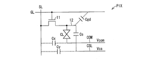
- the plurality of picture elements PIX are arranged in a matrix to form a picture element array, and each picture element PIX includes a TFT 11, a liquid crystal capacitor CL, and an auxiliary capacitor Cs as shown in FIG.
- the TFT 11 has a gate connected to the gate line GL, a source connected to the source line SL, and a drain connected to the pixel electrode 12.
- the liquid crystal capacitor CL is a capacitor in which a liquid crystal layer is disposed between the picture element electrode 12 and the counter electrode COM.
- the auxiliary capacitor Cs is a capacitor in which an insulating film is disposed between the pixel electrode 12 and the auxiliary capacitor line CSL.
- a common potential Vcom generated by a power supply circuit included in the external drive circuit 6 is applied to the counter electrode COM.
- This power supply circuit can switch and output a first common potential Vcom1 and a second common potential Vcom2, which will be described later, as the common potential Vcom.
- This switching can be realized, for example, by switching between the output of the first common potential Vcom1 and the output of the second common potential Vcom2 by a switch circuit and connecting to the common electrode COM.
- the auxiliary capacitance line CSL... Is generated from the high level voltage Vcsh and the low level voltage Vcsl generated by the power supply circuit included in the external drive circuit 6 and supplied to the auxiliary capacitance line drive circuit 5.
- the auxiliary capacitance potential Vcs generated for each auxiliary capacitance line CSL is applied.
- the voltage Vcsh and the voltage Vcsl are switched and applied to each auxiliary capacitance line CSL for each frame.
- the liquid crystal capacitor CL and the auxiliary capacitor Cs constitute a picture element capacity.
- a parasitic capacity Cgd formed between the picture element electrode 12 and the gate line GL is opposed to the pixel capacity.
- the parasitic capacitance Cx ⁇ Cy is also present in the conventional FIG.
- the external drive circuit 6 supplies the gate driver 3 with the gate clock signal GCK and the gate start pulse GSP and supplies the source driver 4 with the source in addition to supplying the above-described common potential Vcom and the auxiliary capacitor potential Vcs with voltages Vcsh and Vcsl.
- a clock signal SCK, a source start pulse SSP, and display data DA are supplied.
- source switches SW (SW1 to SW2) as switches are provided between the data signal output terminal of the source driver 4 and the source line SL.
- each source switch SW includes one data signal output terminal and a plurality of source lines SL such as RGB. And one provided between each of the two is simply shown.
- each horizontal RGB data signal forming one set is supplied to each source in a time division manner from one data signal output terminal assigned to each set through each source switch for branching. Output to line SL.
- the source switch SW is not necessarily required. For example, a configuration in which the output amplifier of the source driver 4 switches between a state where output is possible and a state where output is impossible is considered.
- the source switch SW is composed of, for example, a TFT, and is connected between the output of the output amplifier 4a of the source driver 4 and the source line SL.
- the ON / OFF control of the source switch SW is performed by a control signal s0 supplied from the external drive circuit 6.
- the source switch SW is typically built monolithically on the display panel.
- the source driver 4 is typically configured as an IC, but may be monolithically formed on the display panel. These forms are suitable for a panel using, for example, polycrystalline silicon, CG silicon, microcrystalline silicon, or the like.
- the source switch SW may be provided inside the source driver 4 configured as an IC, or may be provided outside the display panel. This form is suitable for a panel using amorphous silicon, for example.
- the source switch SW is not limited to the TFT, and any type of switch such as a general field effect transistor or bipolar transistor can be used.
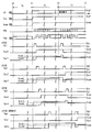
- Fig. 1 shows the operation waveforms when the liquid crystal display device is started up.
- FIG. 1 shows driving waveforms for each gate line GL from the start of power-on to the second frame of the liquid crystal display device.
- the display period starts at time t1.
- the control signal s0 of the source switch SW becomes active (High level in this example).
- the source switch SW is driven ON / OFF by time-division driving. Become.
- the source output from the output stage of the source driver 4 becomes active.
- the first frame F1 is started at time t1.
- the display data to be written to the picture element PIX in the first row is the display data that becomes positive with respect to the common potential Vcom in the second frame F2 or later which is the normal operation period.
- the drive to invert the polarity of the display data one row at a time after the next row is performed.
- the normal operation period is a period during which a normal operation for displaying an image is performed.
- the picture element electrode 12 In the power-off state until the power is turned on, the picture element electrode 12 is approximately settled at the GND potential via the TFT 11 in the high impedance state, the source line SL, and the source switch SW or the source output in the high impedance state. ing.
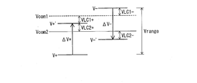
- the common potential Vcom in the first frame F1, is set to the first common potential Vcom1 that is higher than the second common potential Vcom2, which is a common potential in the second and subsequent frames.
- the auxiliary capacitance line CSL In the power-off state until the power is turned on, the auxiliary capacitance line CSL is also substantially at the GND potential (Low level), and the auxiliary capacitance potential Vcs starts from the Low level when the device is activated and in the first frame.
- a later-described first potential as the common potential Vcom is applied to the picture element electrode 12 in the normal operation period (after time t2).
- a data signal potential Vda for black display having a positive polarity with respect to the two common potential Vcom2 is supplied.
- the pixel electrode potential Vdr becomes the potential (first potential) V + by the data signal potential Vda supplied during the selection period.
- the potential V + is set lower than the first common potential Vcom1.
- the auxiliary capacitance potential Vcs1 applied to the auxiliary capacitance wiring CSL1 in the first row changes from the previous Low level (Vcsl) to the High level (Vcsh). And change. Due to the change in the increase applied to the auxiliary capacitance potential Vcs1, the pixel electrode potential Vdr1 is pushed up by ⁇ V + to become a potential (second potential) V + ′. At this time, the relationship between the first common potential Vcom1 and the auxiliary capacitance potential Vcs1 is set so that the potential V + 'is lower than the first common potential Vcom1.
- the potential difference Vcom1-V + ′ which is the absolute value of the difference between the pixel electrode potential Vdr1 and the first common potential Vcom1, becomes the liquid crystal application voltage VLC1 + of the black display level, whereby black display in the first row is performed.
- the liquid crystal applied voltage VLC1 + in the first row in the first frame F1 and thus in the odd-numbered row in the first frame F1, is black display data that is positive with respect to the second common potential Vcom2 in the normal operation period. Is used to obtain a negative polarity writing voltage with respect to the first common potential Vcom1.
- the process proceeds to the next horizontal period, and during the selection period of the picture element PIX in which the gate high potential Vgh is supplied as the scanning signal Vg2 to the gate line GL2 in the second row, the normal operation period is applied to the picture element electrode 12. Then, the black display data signal potential Vda having a negative polarity with respect to the second common potential Vcom is supplied. As shown in FIG. 2, the pixel electrode potential Vdr2 becomes the potential (third potential) V ⁇ by the data signal potential Vda supplied during the selection period. The potential V ⁇ is set higher than the first common potential Vcom1.
- the auxiliary capacitance potential Vcs2 applied to the auxiliary capacitance line CSL2 in the second row is not changed, and the auxiliary capacitance potential Vcs2 is low until then. Since the level (Vcsl: GND potential, for example) is continued, the picture element electrode potential Vdr2 is not subjected to the push-down. At this time, the potential difference (V ⁇ ) ⁇ Vcom1 that is the absolute value of the difference between the pixel electrode potential Vdr2 and the first common potential Vcom1 becomes the liquid crystal application voltage VLC1 ⁇ at the black display level, whereby black display in the second row is performed. Is done.
- the liquid crystal applied voltage VLC1- in the second row in the first frame F1, and thus in the even-numbered row in the first frame F1, is for black display that has a negative polarity with respect to the second common potential Vcom2 in the normal operation period.
- the odd-numbered picture element PIX is the same as the first-line picture element PIX, and the even-numbered picture element PIX is the second-line picture element. Similar to PIX, the pixel electrode potential Vdr is determined.
- the second frame F2 is started. Thereby, the normal operation period is started.
- the control signal s0 remains active.
- the common potential Vcom is set to the second common potential Vcom2.
- the black display data signal potential Vda is supplied to the pixel electrode 12.
- the pixel electrode potential Vdr becomes the potential V ⁇ by the data signal potential Vda supplied during the selection period.
- the pixel electrode potential Vdr1 Due to the change in increase applied to the auxiliary capacitance potential Vcs1, the pixel electrode potential Vdr1 is pushed down by ⁇ V ⁇ to become the potential (fourth potential) V ⁇ ′.
- the relationship between the second common potential Vcom2 and the auxiliary capacitance potential Vcs1 is set so that the potential V- 'is lower than the second common potential Vcom2.
- the potential difference Vcom2- (V ⁇ ′) which is the absolute value of the difference between the pixel electrode potential Vdr1 and the second common potential Vcom2, becomes the liquid crystal application voltage VLC2 ⁇ at the black display level. Display is performed.
- the liquid crystal applied voltage VLC2- in the first row in the second frame F2, and thus in the odd-numbered row in the second frame F2, is for black display having a negative polarity with respect to the second common potential Vcom in the normal operation period.
- the data is used as a voltage having a negative writing polarity with respect to the second common potential Vcom.
- the process proceeds to the next horizontal period, and during the selection period of the picture element PIX in which the gate high potential Vgh is supplied as the scanning signal Vg2 to the gate line GL2 in the second row, the pixel electrode 12 has positive polarity.
- the black display data signal potential Vda is supplied.
- the pixel electrode potential Vdr becomes the potential V + by the data signal potential Vda supplied during the selection period.
- the pixel electrode potential Vdr1 Due to the change in the increase applied to the auxiliary capacitance potential Vcs2, the pixel electrode potential Vdr1 is pushed up by ⁇ V + to become the potential V + ′.
- the relationship between the second common potential Vcom2 and the auxiliary capacitance potential Vcs2 is set so that the potential V + 'is higher than the second common potential Vcom2.
- the potential difference (V + ′) ⁇ Vcom2 which is the absolute value of the difference between the pixel electrode potential Vdr1 and the second common potential Vcom2, becomes the liquid crystal application voltage VLC2 + at the black display level, whereby the black display in the second row is performed. Done.
- the liquid crystal applied voltage VLC2 + in the second row in the second frame F2, and thus in the even-numbered row in the second frame F2, is black display data that is positive with respect to the second common potential Vcom in the normal operation period. Is used as a voltage having a positive polarity for the second common potential Vcom.
- the odd-numbered picture element PIX is the same as the first-line picture element PIX
- the even-numbered picture element PIX is the second-line picture element. Similar to PIX, the pixel electrode potential Vdr is determined. Further, after the third frame F3, the operation is performed on the same principle as that of the second frame F2, while inverting the polarity of the data signal da of each picture element with respect to the common potential Vcom of the own frame from that of the previous frame.
- the potential difference (V ⁇ ) ⁇ Vcom2 in FIG. 2 is typically a large value as described for the potential difference (V ⁇ ) ⁇ Vcom in FIG. 7, and the liquid crystal at the time of black display in FIG. It is sufficiently larger than the applied voltage VLC2 + and the liquid crystal applied voltage VLC2-.
- the liquid crystal applied voltage VLC1 + and the liquid crystal applied voltage VLC1- in the first frame F1 are smaller than the potential difference Vcom2- (V +) and the potential difference (V ⁇ ) ⁇ Vcom2, the liquid crystal applied voltage in the first frame F1 is positive.
- the black display voltage can be set smaller than the gray display voltage.
- the first common potential is defined between the potential V + ′ and the potential V ⁇ . Since the common potential is set, the liquid crystal application voltage having a positive writing polarity with respect to the first common potential and the liquid crystal application voltage having a negative writing polarity with respect to the first common potential are close to each other. Therefore, as in the prior art shown in FIG. 7, the liquid crystal application voltages in the odd and even rows have the same write polarity even though the data signal potentials for different polarities are given. The pixel electrode potential due to the data signal potential for one polarity is not greatly separated from the common potential.
- the display screen of the first frame F1 can avoid displaying a striped pattern composed of black display rows and gray display rows as shown in FIG.
- the value of the first common potential Vcom1 is set between the potential V + ′ and the potential V ⁇ .
- the liquid crystal applied voltage VLC1 + and the liquid crystal applied voltage VLC1- are equally close to the liquid crystal applied voltage VLC2 + and the liquid crystal applied voltage VLC2- for black display. Display can be made. In particular, in the case of normally black, black display is obtained when the liquid crystal applied voltage is below the threshold voltage.
- the liquid crystal applied voltages VLC2 +, VLC2 ⁇ can also correspond to the equivalent black display level. Further, if the liquid crystal applied voltages VLC2 + and VLC2- and the liquid crystal applied voltages VLC1 + and VLC1- are gray display levels other than the black display level, etc., if the inequality (1) holds, the liquid crystal applied voltages VLC2 + and VLC2- Since the liquid crystal applied voltages VLC1 + and VLC1- are close to each other, it is effective for displaying some constant color in a predetermined period after the apparatus is started.
- liquid crystal applied voltage VLC1 + and the liquid crystal applied voltage VLC1- do not necessarily have to be equal to each other as long as they are at a sufficient black display level, but are equal to each other between pixels having different polarities in the first frame F1. This is preferable in that the black display level is accurately aligned.
- the liquid crystal applied voltage VLC2 + and the liquid crystal applied voltage VLC2- do not necessarily have to be equal to each other, but the effective value of the positive polarity liquid crystal applied voltage and the effective value of the negative polarity liquid crystal applied voltage are equal to each other.
- display luminance is uniform between picture elements having different polarities in the same frame.
- the common potential Vcom is set to the first common potential Vcom1 in the first frame F1
- the data signal potential Vda to be used is the same as that in the normal operation period.
- the entire data signal potential range Vrange of the negative data signal potential range and the negative data signal potential need not be particularly widened.
- the conventional data signal potential range Vrange can be used as it is.
- the gate line inversion drive is performed.
- the present invention is not limited to this.
- the liquid crystal display device performs the AC drive in which the data signal potentials having the same polarity are written to all the picture elements PIX in the same row. It's okay.
- the display device of the present invention provides An active matrix type display device having an auxiliary capacity wiring for switching between a high level and a low level of an auxiliary capacity potential every frame,
- the common potential can be switched between a first common potential and a second common potential, and the first common potential is higher than the second common potential.
- the auxiliary capacitance potential starts from the low level.
- all the pixels in the same row have the same writing polarity with respect to the first common potential, and are written to the first common potential.
- the pixel electrode potential becomes the first potential during the selection period for the row of the pixel having the negative polarity for the first common potential.
- the first potential is set lower than the first common potential.
- the storage capacitor potential changes from the low level to the high level. Due to the change in the increase given to the auxiliary capacitance potential, the pixel electrode potential is pushed up to become the second potential. At this time, the second potential is lower than the first common potential.
- the potential difference between the pixel electrode potential and the first common potential at this time becomes a liquid crystal application voltage having a writing polarity of a negative polarity with respect to the first common potential, thereby displaying the first frame.
- the pixel electrode potential becomes the third potential by the data signal potential supplied in the selection period.
- the third potential is set higher than the first common potential.
- the selection period ends, the storage capacitor potential continues to the previous Low level, so that the pixel electrode potential is not pushed down.
- the potential difference between the pixel electrode potential and the common potential at this time becomes a liquid crystal application voltage having a writing polarity having a positive polarity with respect to the first common potential, thereby displaying the first frame.
- the first common potential is set between the second potential and the third potential. Therefore, the liquid crystal applied voltage having a positive polarity with respect to the first common potential and the liquid crystal applied voltage having a negative polarity with respect to the first common potential are close to each other. Therefore, as in the prior art, the pixel electrode potential due to the data signal potential for one polarity is greatly separated from the common potential between the rows to which data signal potentials for different polarities are applied, with the same writing polarity. There is no.
- the data signal supplied to the first frame is a data signal for black display.
- the above invention it is possible to avoid the occurrence of a striped pattern composed of black display rows and gray display rows when the apparatus is activated.
- black display is obtained when the liquid crystal applied voltage is equal to or lower than the threshold voltage. Therefore, the liquid crystal applied voltage due to the difference between the second potential and the first common potential, the third potential, and the first common are displayed. There is an effect that the liquid crystal applied voltage due to the difference from the potential can be easily made to correspond to the equivalent black display level.
- the display device of the present invention provides After the second frame,
- the second common potential is used as a common potential so that all picture elements in the same row have the same writing polarity with respect to the second common potential, and in the same frame, with respect to the second common potential.
- a data signal is supplied and AC driven so that there are rows of picture elements with different writing polarities, For a row of picture elements having a positive polarity for writing with respect to the second common potential, a data signal having the first potential is supplied, and a pixel writing period is set for the corresponding auxiliary capacitance wiring.
- the pixel electrode potential is changed to the second potential.
- a data signal of the third potential is supplied, and a picture element writing period is set for the corresponding auxiliary capacitance wiring.
- the pixel electrode potential is changed to a fourth potential lower than the second common potential by changing the auxiliary capacitance potential from the High level to the Low level.
- the same color display in the second and subsequent frames, the same color display can be performed using the data signal having the same first potential as that in the first frame and the third data signal. Therefore, there is an effect that it is not necessary to expand the range of the data signal potential when realizing the first frame with high display quality.
- the display device of the present invention provides The absolute value of the difference between the second potential and the first common potential is VLC1 +, the absolute value of the difference between the third potential and the first common potential is VLC1-, the second potential and the second potential. If the absolute value of the difference from the common potential is VLC2 +, and the absolute value of the difference between the fourth potential and the second common potential is VLC2- VLC2 +, VLC2- ⁇ VLC1 +, VLC1- ⁇ (Third potential)-(Second common potential) It is characterized by being.
- the liquid crystal applied voltage VLC1 + and the liquid crystal applied voltage VLC1- are equally close to the liquid crystal applied voltage VLC2 + and the liquid crystal applied voltage VLC2- for black display, and even more uniform black display is performed at startup.
- black display can be obtained when the applied voltage of the liquid crystal is lower than the threshold voltage. Therefore, VLC1 +, VLC1- ⁇ (third potential) ⁇ (second common potential).
- the applied voltages VLC2 + and VLC2- and the liquid crystal applied voltages VLC1 + and VLC1- both have the effect of corresponding to an equivalent black display level.
- the liquid crystal applied voltages VLC2 + and VLC2- and the liquid crystal applied voltages VLC1 + and VLC1- are set to gray display levels other than the black display level, the liquid crystal applied voltages VLC2 + and VLC2- and the liquid crystal applied Since the voltages VLC1 + and VLC1- are close to each other, there is an effect that the voltage VLC1 + and VLC1- are effective for displaying some constant color in a predetermined period after the apparatus is activated.
- the display device driving method of the present invention provides: A driving method of a display device for driving an active matrix type display device having an auxiliary capacitance wiring for switching between a high level and a low level of an auxiliary capacitance potential every frame, The common potential is switched between a first common potential and a second common potential, and the first common potential is higher than the second common potential, In the first frame after the device power is turned on, the auxiliary capacitance potential starts from the low level. Using the first common potential as the common potential, all the pixels in the same row have the same writing polarity with respect to the first common potential, and are written to the first common potential.
- the pixel electrode potential becomes the first potential during the selection period for the row of the pixel having a negative polarity for the first common potential.
- the first potential is set lower than the first common potential.
- the storage capacitor potential changes from the low level to the high level. Due to the change in the increase given to the auxiliary capacitance potential, the pixel electrode potential is pushed up to become the second potential. At this time, the second potential is lower than the first common potential.
- the potential difference between the pixel electrode potential and the first common potential at this time becomes a liquid crystal application voltage having a writing polarity having a negative polarity with respect to the first common potential, whereby the display of the first frame is performed.
- the pixel electrode potential becomes the third potential by the data signal potential supplied in the selection period.
- the third potential is set higher than the first common potential.
- the selection period ends, the storage capacitor potential continues to the previous Low level, so that the pixel electrode potential is not pushed down.
- the potential difference between the pixel electrode potential and the common potential at this time becomes a liquid crystal application voltage having a writing polarity having a positive polarity with respect to the first common potential, thereby displaying the first frame.
- the first common potential is set between the second potential and the third potential. Therefore, the liquid crystal applied voltage having a positive polarity with respect to the first common potential and the liquid crystal applied voltage having a negative polarity with respect to the first common potential are close to each other. Therefore, as in the prior art, the pixel electrode potential due to the data signal potential for one polarity is greatly separated from the common potential between the rows to which data signal potentials for different polarities are applied, with the same writing polarity. There is no.
- the display device driving method of the present invention provides:
- the data signal supplied to the first frame is a data signal for black display.
- the above invention it is possible to avoid the occurrence of a striped pattern composed of black display rows and gray display rows when the apparatus is activated.
- black display is obtained when the liquid crystal applied voltage is equal to or lower than the threshold voltage. Therefore, the liquid crystal applied voltage due to the difference between the second potential and the first common potential, the third potential, and the first common are displayed. There is an effect that the liquid crystal applied voltage due to the difference from the potential can be easily made to correspond to the equivalent black display level.
- the display device driving method of the present invention provides: After the second frame, The second common potential is used as a common potential so that all picture elements in the same row have the same writing polarity with respect to the second common potential, and in the same frame, with respect to the second common potential.
- a data signal is supplied and AC driven so that there are rows of picture elements with different writing polarities, For a row of picture elements having a positive polarity for writing with respect to the second common potential, a data signal having the first potential is supplied, and a pixel writing period is set for the corresponding auxiliary capacitance wiring.
- the pixel electrode potential is changed to the second potential.
- a data signal of the third potential is supplied, and a picture element writing period is set for the corresponding auxiliary capacitance wiring.
- the pixel electrode potential is changed to a fourth potential lower than the second common potential by changing the auxiliary capacitance potential from the High level to the Low level.
- the same color display in the second and subsequent frames, the same color display can be performed using the data signal having the same first potential as that in the first frame and the third data signal. Therefore, there is an effect that it is not necessary to expand the range of the data signal potential when realizing the first frame with high display quality.
- the display device driving method of the present invention provides: The absolute value of the difference between the second potential and the first common potential is VLC1 +, the absolute value of the difference between the third potential and the first common potential is VLC1-, the second potential and the second potential. If the absolute value of the difference from the common potential is VLC2 +, and the absolute value of the difference between the fourth potential and the second common potential is VLC2- VLC2 +, VLC2- ⁇ VLC1 +, VLC1- ⁇ (Third potential)-(Second common potential) It is characterized by being.
- the liquid crystal applied voltage VLC1 + and the liquid crystal applied voltage VLC1- are equally close to the liquid crystal applied voltage VLC2 + and the liquid crystal applied voltage VLC2- for black display, and even more uniform black display is performed at startup.
- black display can be obtained when the applied voltage of the liquid crystal is lower than the threshold voltage. Therefore, VLC1 +, VLC1- ⁇ (third potential) ⁇ (second common potential).
- the applied voltages VLC2 + and VLC2- and the liquid crystal applied voltages VLC1 + and VLC1- both have the effect of corresponding to an equivalent black display level.
- the liquid crystal applied voltages VLC2 + and VLC2- and the liquid crystal applied voltages VLC1 + and VLC1- are set to gray display levels other than the black display level, the liquid crystal applied voltages VLC2 + and VLC2- and the liquid crystal applied Since the voltages VLC1 + and VLC1- are close to each other, there is an effect that the voltage VLC1 + and VLC1- are effective for displaying some constant color in a predetermined period after the apparatus is activated.
- the present invention can be suitably used for various display devices including a liquid crystal display device.
- Liquid crystal display device (display device) CSL auxiliary capacitance wiring F1 first frame F2 second frame PIX picture element Vcom common potential Vcom1 first common potential Vcom2 second common potential Vdr pixel electrode potential Vcs auxiliary capacitance potential V + potential (first potential) V + 'potential (second potential) V- potential (third potential) V- 'potential (fourth potential)
Abstract
本発明は、補助容量配線を駆動する表示装置に関する。 本発明の表示装置では、電源投入後の第1フレーム(F1)において、第2コモン電位(Vcom2)よりも高い第1コモン電位(Vcom1)を使用して、同一の行の全絵素が互いに同じ書き込み極性となり、書き込み極性が互いに異なる絵素の行が存在するようにし、負の書き込み極性となる行については、第1コモン電位(Vcom1)よりも低い第1の電位(V+)のデータ信号を供給し、選択期間の終了後に補助容量電位(Vcs1)をLow(Vcsl)からHigh(Vcsh)へ変化させて、絵素電極電位(Vdr1)を第2コモン電位(Vcom2)よりも高く第1コモン電位(Vcom1)よりも低い第2の電位(V+’)に変化させ、正の書き込み極性となる行については、第1コモン電位(Vcom1)よりも高い第3の電位(V-)のデータ信号を供給し、選択期間の終了後に補助容量電位(Vcs1)をLow(Vcsl)のままとする。 本発明によると、液晶表示装置の起動時における表示品位の低下を回避することができる。
Description
本発明は、補助容量配線を駆動する表示装置に関する。
ゲートライン反転駆動のような同じ行の表示データの極性が互いに同じとなる交流駆動が行われる液晶表示装置では、各行に配置された補助容量配線を行ごとに駆動することにより、データ信号電位範囲を狭めながら、液晶印加電圧を大きくすることができる利点がある。
図6に、このような補助容量配線を駆動する液晶表示装置が備える絵素PIXの構成例を等価回路で示す。
絵素PIXは、絵素PIXの選択素子としてのTFT101、液晶容量CL、および、補助容量Csを備えている。TFT101のゲートはゲートラインGLに、ソースはソースラインSLに、ドレインは絵素電極102に、それぞれ接続されている。液晶容量CLは、絵素電極102と対向電極COMとの間に液晶層が配置されてなる容量である。補助容量Csは、絵素電極102と補助容量配線CSLとの間に絶縁膜が配置されてなる容量である。対向電極COMにはコモン電位Vcomが印加され、補助容量配線CsLにはHighレベルとLowレベルとからなる補助容量電位Vcsが印加される。また、絵素PIXが備える寄生容量として、例えば絵素電極102と走査信号線GLとの間に寄生容量Cgdが形成される。
上記構成の絵素PIXにおいて、TFT101をON状態として絵素電極102にデータ信号電位を書き込んでTFT101をOFF状態にした後に、当該絵素PIXに割り当てられている補助容量配線CsLに印加される補助容量電位Vcsを、LowレベルからHighレベルに変化させると、図7に示すように、補助容量Csを介して絵素電極電位VdrがV+からV+’に突き上げられる。従って、このときの突き上げ量ΔV+によってV+’となった絵素電極電位Vdrがコモン電位Vcomから正の向きに離れるように、コモン電位Vcom、補助容量Cs、補助容量電位Vcsを設定しておけば、供給された正極性のデータ信号電位が低くても、正極性の十分な大きさの液晶印加電圧VLC+を得ることができる。なお、V+は階調レベルに応じて決められ、必ずしもコモン電位Vcomより低くなくてよい。
また、絵素電極102にデータ信号電位を書き込んでTFT101をOFF状態にした後に、補助容量電位Vcsを、HighレベルからLowレベルに変化させると、図7に示すように、補助容量Csを介して絵素電極電位VdrがV-からV-’に突き下げられる。従って、このときの突き下げ量ΔV-によってV-’となった絵素電極電位Vdrがコモン電位Vcomから負の向きに離れるように、補助容量Csや補助容量電位Vcsを設定しておけば、供給された負極性のデータ信号電位が高くても、負極性の十分な大きさの液晶印加電圧VLC-を得ることができる。なお、V-は階調レベルに応じて決められ、必ずしもコモン電位Vcomより高くなくてよい。
従って、コモン電位Vcomを中心に挟むように分布させた正極性のデータ信号電位と負極性のデータ信号電位とを絵素PIXに書き込むことにより得られる絵素電極電位Vdrをそのまま用いる場合よりも、正極性と負極性とを合わせた全体のデータ信号電位範囲Vrangeを狭くすることができる。これにより階調基準電圧を生成する電源電圧を低くすることができるので、液晶表示装置の低消費電力化および駆動の高周波化を図ることができる。
しかしながら、上記従来の液晶表示装置では、電源投入時の表示品位が低下する問題が発生する。以下に、これについて説明する。
図8に、液晶表示装置の起動時の動作波形を示す。
この場合に、液晶表示装置はノーマリブラックでありゲートライン反転駆動されるものとする。図8には液晶表示装置の電源投入開始から2フレーム目までの、各行についての駆動波形が示されている。
まず、時刻t0で装置電源の投入が行われて電源投入期間Tbが経過すると、時刻t1において制御信号s0がアクティブになることにより、各水平期間にソースドライバのデータ信号出力端子への各ソース出力がアクティブとなる表示期間に移行する。同時に、電源回路による補助容量電源電位Ecsおよびコモン電位Vcomの立ち上げが行われる。
表示期間ではまず時刻t1で第1フレームF1が開始される。第1フレームF1においては、データ信号電位極性POLに従って、1行目の絵素PIXに書き込む表示データを正極性とし、次行以降は1行ずつ表示データの極性を反転させていくものとする。次フレーム以降は、各行の絵素PIXに書き込む表示データの極性を、直前フレームの極性に対して反転させる。液晶表示装置がノーマリブラックであるので、表示期間が開始されてから所定フレームまでは、表示データとして、正極性、負極性とも黒表示のデータ信号電位Vdaが各絵素PIXに供給される。
装置電源が投入される時刻t0までの電源OFF状態において、絵素電極102は、ハイインピーダンス状態にあるTFT101、ソースラインSL、および、ハイインピーダンス状態にあるソースドライバの出力を介して概ねGND電位に落ち着いている。時刻t1でコモン電位Vcomが立ち上がり、1行目のゲートラインGL1に走査信号Vg1としてゲートハイ電位Vghが供給されると、絵素電極102には正極性の黒表示のデータ信号電位Vda(例えば0.2V)の書き込みが開始される。データ信号電位Vdaの書き込み後の絵素電極電位Vdrは、図7にV+(例えば0.2V)で示したように、立ち上がったコモン電位Vcom(例えば2V)よりも低いが、走査信号Vg1がゲートロー電位Vglに立ち下がってデータ信号電位Vdaの書き込みが終了すると、1行目の補助容量配線CSL1に印加される補助容量電位Vcs1が、それまでのLowレベル(Vcsl)からHighレベル(Vcsh)へと変化する。これにより、絵素電極電位Vdr1はΔV+(例えば2V)だけ突き上げられて、V+’(例えば2.2V)で示すようにコモン電位Vcomよりも高いレベルになる。このときの絵素電極電位Vdr1とコモン電位Vcomとの電位差(V+’)-Vcom=0.2Vが黒表示レベルの液晶印加電圧VLC+となることで、1行目の黒表示が行われる。
続いて、図8において、次の水平期間に移り、2行目のゲートラインGL2に走査信号Vg2としてゲートハイ電位Vghが供給されると、絵素電極102には負極性の黒表示のデータ信号電位Vda(例えば3.8V)の書き込みが開始される。データ信号電位Vdaの書き込み後の絵素電極電位Vdrは、図7にV-(例えば3.8V)で示すように、立ち上がったコモン電位Vcom(例えば2V)よりも高い。ここで、走査信号Vg1がゲートロー電位Vglに立ち下がってデータ信号電位Vdaの書き込みが終了すると、2行目の補助容量配線CSL1に印加される補助容量電位Vcs1が、それまでのLowレベル(Vcsl:ここではGND電位)を継続するので、液晶印加電圧は図7に示すように正極性の電圧(VLC1-)=(V-)-Vcom=1.8Vとなって、通常動作時の液晶印加電圧VCL-とは異なる。
以降、各水平期間が順次経過するに伴い、奇数行目の絵素PIXには1行目の絵素PIXと同じように、また、偶数行目の絵素PIXには2行目の絵素PIXと同じように、データ信号電位が書き込まれていく。
時刻t2からは第2フレームF2が開始され、第1フレームF1と同様に黒表示のデータ信号が供給されるとすると、奇数行目の絵素PIXには負極性のデータ信号電位Vdaが書き込まれるとともに、偶数行目の絵素PIXには正極性のデータ信号電位Vdaが書き込まれる。
ここで、負極性のデータ信号電位Vdaの書き込みについては、走査信号Vg1がゲートロー電位Vglに立ち下がってデータ信号電位Vdaの書き込みが終了すると、補助容量配線CSLに印加される補助容量電位Vcsが、それまでのHighレベル(Vcsh)からLowレベル(Vcsl)へと変化する。これにより、絵素電極電位Vdrは図7に示すようにΔV-(例えば2V)だけ突き下げられて、V-’(例えば1.8V)で示すようにコモン電位Vcom(例えば2V)よりも低いレベルになる。このときの絵素電極電位Vdr1とコモン電位Vcomとの電位差Vcom-(V-’)=0.2Vが黒表示レベルの液晶印加電圧VLC-となることで黒表示が行われる。
このようにして、次フレーム以降は、フレームごとに表示データの極性を反転させながら第2フレームF2と同様に表示が行われる。
しかしながら、上述したように、第1フレームF1において、負極性の黒表示を行う目的でデータ信号電位Vdaを書き込んだ絵素PIXについては、補助容量電位Vcsが電源起動時からLowレベル(Vcsl=GND電位)であって、絵素電極電位Vdrの突き下げを行うための補助容量電位VcsのHighレベルからLowレベルへの変化を与えることができない。このとき、負極性のデータ信号電位が書き込まれた絵素PIXの液晶印加電圧は(VLC1-)=1.8Vと大きくなるため、当該絵素PIXの実際の表示はグレー表示となる。この結果、第1フレームF1の表示画面には、図9に示すように黒表示の行とグレー表示の行とからなる縞模様が表示される。これは、視覚的には一瞬白くフラッシュする画面となり、表示品位が低下してしまう。
なお、特許文献1には第1フレームよりも前の時点での横筋を解消する技術が開示されているが、第1フレームにおける上記縞模様を解消することはできない。
以上のように、補助容量配線を駆動する従来の液晶表示装置には、装置の起動時に表示品位が低下するという問題があった。
本発明は、上記従来の問題点に鑑みなされたものであり、その目的は、装置の起動時における表示品位の低下を回避することのできる表示装置および表示装置の駆動方法を実現することにある。
本発明の表示装置は、上記課題を解決するために、
1フレームごとに補助容量電位のHighレベルとLowレベルとを切り替える補助容量配線を備えたアクティブマトリクス型の表示装置であって、
コモン電位として、第1コモン電位と第2コモン電位との2通りに切り替えることが可能であって上記第1コモン電位は上記第2コモン電位よりも高く、
補助容量電位がLowレベルから始まる、装置電源の投入後の第1フレームにおいて、
上記コモン電位として上記第1コモン電位を使用して、同じ行の全ての絵素が上記第1コモン電位に対して互いに同じ書き込み極性となるように、かつ、上記第1コモン電位に対して書き込み極性が互いに異なる絵素の行が存在するように、データ信号を供給し、
上記第1コモン電位に対して負極性の書き込み極性となる絵素の行については、上記第1コモン電位よりも低い第1の電位のデータ信号を供給し、対応する上記補助容量配線に対して、絵素の選択期間が終了した後に、補助容量電位をLowレベルからHighレベルへ変化させることにより、絵素電極電位を上記第2コモン電位よりも高く上記第1コモン電位よりも低い第2の電位に変化させ、
上記第1コモン電位に対して正極性の書き込み極性となる絵素の行については、上記第1コモン電位よりも高い第3の電位のデータ信号を供給し、対応する上記補助容量配線に対して、絵素の選択期間が終了した後に、補助容量電位をLowレベルのままとすることを特徴としている。
上記の発明によれば、第1コモン電位に対して負極性の書き込み極性となる絵素の行については、選択期間に絵素電極電位は第1の電位となる。第1の電位は第1コモン電位よりも低く設定されている。選択期間が終了すると、補助容量電位がLowレベルからHighレベルへと変化する。この補助容量電位に与えられる上昇の変化により、絵素電極電位突き上げられて第2の電位となる。このとき、第2の電位が第1コモン電位よりも低い。このときの絵素電極電位と第1コモン電位との電位差が第1コモン電位に対して負極性の書き込み極性の液晶印加電圧となることで、第1フレームの表示が行われる。
また、第1コモン電位に対して正極性の書き込み極性となる絵素の行については、選択期間に供給されたデータ信号電位によって絵素電極電位は第3の電位となる。第3の電位は第1コモン電位よりも高く設定されている。選択期間が終了すると、補助容量電位はそれまでのLowレベルを継続するので、絵素電極電位は突き下げを受けない。このときの絵素電極電位とコモン電位との電位差が第1コモン電位に対して正極性の書き込み極性の液晶印加電圧となることで、第1フレームの表示が行われる。
このように、第1フレームにおいて補助容量電位のHighレベルからLowレベルへの変化が得られなくても、第2の電位と第3の電位との間に第1コモン電位というコモン電位が設定されるので、第1コモン電位に対して正極性の書き込み極性の液晶印加電圧と第1コモン電位に対して負極性の書き込み極性の液晶印加電圧とが互いに近い値になる。従って、従来のように、異なる極性用のデータ信号電位を与えた行どうしで、互いに同じ書き込み極性となって一方の極性用のデータ信号電位による絵素電極電位がコモン電位から大きく離れてしまうことがない。
従って、第1フレームの表示画面に縞模様が表示されることを回避することができる。この結果、装置の起動時における表示品位の低下を回避することのできる表示装置を実現することができるという効果を奏する。
本発明の表示装置の駆動方法は、上記課題を解決するために、
1フレームごとに補助容量電位のHighレベルとLowレベルとを切り替える補助容量配線を備えたアクティブマトリクス型の表示装置を駆動する、表示装置の駆動方法であって、
コモン電位を第1コモン電位と第2コモン電位との2通りに切り替え、上記第1コモン電位は上記第2コモン電位よりも高く、
補助容量電位がLowレベルから始まる、装置電源の投入後の第1フレームにおいて、
上記コモン電位として上記第1コモン電位を使用して、同じ行の全ての絵素が上記第1コモン電位に対して互いに同じ書き込み極性となるように、かつ、上記第1コモン電位に対して書き込み極性が互いに異なる絵素の行が存在するように、データ信号を供給し、
上記第1コモン電位に対して負極性の書き込み極性となる絵素の行については、上記第1コモン電位よりも低い第1の電位のデータ信号を供給し、対応する上記補助容量配線に対して、絵素の選択期間が終了した後に、補助容量電位をLowレベルからHighレベルへ変化させることにより、絵素電極電位を上記第2コモン電位よりも高く上記第1コモン電位よりも低い第2の電位に変化させ、
上記第1コモン電位に対して正極性の書き込み極性となる絵素の行については、上記第1コモン電位よりも高い第3の電位のデータ信号を供給し、対応する上記補助容量配線に対して、絵素の選択期間が終了した後に、補助容量電位をLowレベルのままとすることを特徴としている。
上記の発明によれば、第1コモン電位に対して負極性の書き込み極性となる絵素の行については、選択期間に絵素電極電位は第1の電位となる。第1の電位は第1コモン電位よりも低く設定されている。選択期間が終了すると、補助容量電位がLowレベルからHighレベルへと変化する。この補助容量電位に与えられる上昇の変化により、絵素電極電位突き上げられて第2の電位となる。このとき、第2の電位が第1コモン電位よりも低い。このときの絵素電極電位と第1コモン電位との電位差が第1コモン電位に対して負極性の書き込み極性の液晶印加電圧となることで、第1フレームの表示が行われる。
また、第1コモン電位に対して正極性の書き込み極性となる絵素の行については、選択期間に供給されたデータ信号電位によって絵素電極電位は第3の電位となる。第3の電位は第1コモン電位よりも高く設定されている。選択期間が終了すると、補助容量電位はそれまでのLowレベルを継続するので、絵素電極電位は突き下げを受けない。このときの絵素電極電位とコモン電位との電位差が第1コモン電位に対して正極性の書き込み極性の液晶印加電圧となることで、第1フレームの表示が行われる。
このように、第1フレームにおいて補助容量電位のHighレベルからLowレベルへの変化が得られなくても、第2の電位と第3の電位との間に第1コモン電位というコモン電位が設定されるので、第1コモン電位に対して正極性の書き込み極性の液晶印加電圧と第1コモン電位に対して負極性の書き込み極性の液晶印加電圧とが互いに近い値になる。従って、従来のように、異なる極性用のデータ信号電位を与えた行どうしで、互いに同じ書き込み極性となって一方の極性用のデータ信号電位による絵素電極電位がコモン電位から大きく離れてしまうことがない。
従って、第1フレームの表示画面に縞模様が表示されることを回避することができる。この結果、装置の起動時における表示品位の低下を回避することのできる表示装置の駆動方法を実現することができるという効果を奏する。
本発明の表示装置は、以上のように、
1フレームごとに補助容量電位のHighレベルとLowレベルとを切り替える補助容量配線を備えたアクティブマトリクス型の表示装置であって、
コモン電位として、第1コモン電位と第2コモン電位との2通りに切り替えることが可能であって上記第1コモン電位は上記第2コモン電位よりも高く、
補助容量電位がLowレベルから始まる、装置電源の投入後の第1フレームにおいて、
上記コモン電位として上記第1コモン電位を使用して、同じ行の全ての絵素が上記第1コモン電位に対して互いに同じ書き込み極性となるように、かつ、上記第1コモン電位に対して書き込み極性が互いに異なる絵素の行が存在するように、データ信号を供給し、
上記第1コモン電位に対して負極性の書き込み極性となる絵素の行については、上記第1コモン電位よりも低い第1の電位のデータ信号を供給し、対応する上記補助容量配線に対して、絵素の選択期間が終了した後に、補助容量電位をLowレベルからHighレベルへ変化させることにより、絵素電極電位を上記第2コモン電位よりも高く上記第1コモン電位よりも低い第2の電位に変化させ、
上記第1コモン電位に対して正極性の書き込み極性となる絵素の行については、上記第1コモン電位よりも高い第3の電位のデータ信号を供給し、対応する上記補助容量配線に対して、絵素の選択期間が終了した後に、補助容量電位をLowレベルのままとする。
この結果、装置の起動時における表示品位の低下を回避することのできる表示装置を実現することができるという効果を奏する。
本発明の表示装置の駆動方法は、以上のように、
1フレームごとに補助容量電位のHighレベルとLowレベルとを切り替える補助容量配線を備えたアクティブマトリクス型の表示装置を駆動する、表示装置の駆動方法であって、
コモン電位を第1コモン電位と第2コモン電位との2通りに切り替え、上記第1コモン電位は上記第2コモン電位よりも高く、
補助容量電位がLowレベルから始まる、装置電源の投入後の第1フレームにおいて、
上記コモン電位として上記第1コモン電位を使用して、同じ行の全ての絵素が上記第1コモン電位に対して互いに同じ書き込み極性となるように、かつ、上記第1コモン電位に対して書き込み極性が互いに異なる絵素の行が存在するように、データ信号を供給し、
上記第1コモン電位に対して負極性の書き込み極性となる絵素の行については、上記第1コモン電位よりも低い第1の電位のデータ信号を供給し、対応する上記補助容量配線に対して、絵素の選択期間が終了した後に、補助容量電位をLowレベルからHighレベルへ変化させることにより、絵素電極電位を上記第2コモン電位よりも高く上記第1コモン電位よりも低い第2の電位に変化させ、
上記第1コモン電位に対して正極性の書き込み極性となる絵素の行については、上記第1コモン電位よりも高い第3の電位のデータ信号を供給し、対応する上記補助容量配線に対して、絵素の選択期間が終了した後に、補助容量電位をLowレベルのままとする。
この結果、装置の起動時における表示品位の低下を回避することのできる表示装置の駆動方法を実現することができるという効果を奏する。
本発明の実施形態について、図1~図5を用いて説明すれば以下の通りである。
図3に、本実施形態に係る液晶表示装置(表示装置)1の構成を示す。
液晶表示装置1はアクティブマトリクス型の表示装置であり、表示部2と、走査信号線駆動回路としてのゲートドライバ3と、データ信号線駆動回路としてのソースドライバ4と、補助容量配線駆動回路5と、ゲートドライバ3、ソースドライバ4、補助容量配線駆動回路5、および対向電極COMを駆動制御するための外部駆動回路6とを備えている。この液晶表示装置1は、交流駆動としてゲートライン反転駆動を行う。そして、さらに、正極性データをパネルに供給する期間と負極性データをパネルに供給する期間とで、互いに補助容量配線CSL(後述)に印加する補助容量電位Vcsの極性を反転させる駆動を、補助容量配線CSLごとに行う。
表示部2は、複数本(n本)の走査信号線としてのゲートラインGL…(GL1~GLn)と、ゲートラインGL…のそれぞれと交差する複数本(m本)のデータ信号線としてのソースラインSL…(SL1~SLm)と、ゲートラインGL…とソースラインSL…との各交差点にそれぞれ対応して設けられた複数個(n×m個)の絵素PIX…とを含む。また、ここでは図示しないが、表示部2は、ゲートラインGL…と平行に補助容量配線CSL…(CSL1~CSLn)を備えており、当該方向に並んだm個の絵素PIX…からなる各絵素行に1本の補助容量配線CSLが割り当てられている。
複数の絵素PIX…はマトリクス状に配置されて絵素アレイを構成し、各絵素PIXは、図4に示すように、TFT11と、液晶容量CLと、補助容量Csとを備えている。TFT11のゲートはゲートラインGLに、ソースはソースラインSLに、ドレインは絵素電極12にそれぞれ接続されている。液晶容量CLは、絵素電極12と対向電極COMとの間に液晶層が配置されてなる容量である。補助容量Csは、絵素電極12と補助容量配線CSLとの間に絶縁膜が配置されてなる容量である。対向電極COMには外部駆動回路6が備える電源回路で生成されたコモン電位Vcomが印加される。この電源回路は、コモン電位Vcomとして後述する第1コモン電位Vcom1と第2コモン電位Vcom2とを切り替えて出力することが可能である。この切り替えは、例えばスイッチ回路によって第1コモン電位Vcom1の出力と第2コモン電位Vcom2の出力とを切り替えてコモン電極COMに接続することで実現可能である。補助容量配線CSL…には、外部駆動回路6が備える電源回路で生成されて補助容量配線駆動回路5に供給されたHighレベルの電圧VcshとLowレベルの電圧Vcslとから、補助容量配線駆動回路5によって補助容量配線CSLごとに生成された補助容量電位Vcsが印加される。各補助容量配線CSLには、1フレームごとに、電圧Vcshと電圧Vcslとが切り替えられて印加される。液晶容量CLと補助容量Csとは絵素容量を構成しているが、絵素容量を構成する他の容量として、絵素電極12とゲートラインGLとの間に形成される寄生容量Cgd、対向電極COMとソースラインSLとの間に形成される寄生容量Cx、補助容量配線CSLとソースラインSLとの間に形成される寄生容量Cyなどが存在する。寄生容量Cx・Cyは、従来の図6でも存在するものである。
外部駆動回路6は、上述のコモン電位Vcomや補助容量電位Vcsの電圧Vcsh・Vcslを供給する他に、ゲートドライバ3にゲートクロック信号GCKおよびゲートスタートパルスGSPを供給するとともに、ソースドライバ4にソースクロック信号SCK、ソーススタートパルスSSP、および、表示データDAを供給する。
また、ソースドライバ4のデータ信号出力端子とソースラインSLとの間には、スイッチとしてのソーススイッチSW(SW1~SW2)が設けられている。なお、ここでは、本発明の表示装置としてSSD(Source Sharing Drive)方式で駆動されるものを例として考え、各ソーススイッチSWが、1つのデータ信号出力端子とRGBなどの複数のソースラインSL…とのそれぞれの間に1つずつ設けられるものを簡略的に示したものとする。SSD方式の駆動では、各水平期間において、1組をなすRGBの各色のデータ信号を、組ごとに割り当てられた1つのデータ信号出力端子から分岐用の各ソーススイッチを介して時分割で各ソースラインSLに出力する。SSD方式以外で駆動される表示装置ではソーススイッチSWは必ずしもなくてよく、例えばソースドライバ4の出力アンプが出力可能な状態と出力不能の状態との間で切り替わる構成を考える。
図5に示すように、ソーススイッチSWは例えばTFTで構成されており、ソースドライバ4の出力アンプ4aの出力とソースラインSLとの間に接続されている。ソーススイッチSWのON/OFF制御は、外部駆動回路6から供給される制御信号s0によって行われる。この場合には、ソーススイッチSWは典型的には表示パネル上にモノリシックに作り込まれる。またこの場合に、ソースドライバ4は典型的にはICとして構成されるが、表示パネル上にモノリシックに作り込まれてもよい。これらの形態は、例えば多結晶シリコン、CGシリコン、微結晶シリコンなどを用いたパネルに適している。
また、ソーススイッチSWは、ICとして構成されるソースドライバ4の内部に備えられていてもよいし、表示パネルの外部に設けられてもよい。この形態は、例えばアモルファスシリコンを用いたパネルに適している。ソーススイッチSWとしてはTFTに限らず、一般の電界効果トランジスタやバイポーラトランジスタなどの任意の形態のスイッチが使用可能である。
次に、上記の構成の液晶表示装置1について、装置の起動時の動作を以下に説明する。
図1に、液晶表示装置の起動時の動作波形を示す。
この場合に、液晶表示装置はノーマリブラックであるとする。図1には液晶表示装置の電源投入開始から2フレーム目までの、各ゲートラインGLについての駆動波形が示されている。
まず、時刻t0で装置電源の投入が行われて電源投入期間Tbが経過すると、時刻t1において表示期間に移行する。このときに、同時にソーススイッチSWの制御信号s0がアクティブ(この例ではHighレベル)になり、SSD方式の駆動方式の場合には、ソーススイッチSWは時分割駆動によりON/OFF駆動される状態となる。また、ソーススイッチSWが設けられていない場合には、ソースドライバ4の出力段からのソース出力がアクティブになる。
また、時刻t1には、同時に、外部駆動回路6に備えられた電源回路による補助容量電源電位Ecsおよびコモン電位Vcomの立ち上げが行われる。
表示期間ではまず時刻t1で第1フレームF1が開始される。第1フレームF1においては、データ信号電位極性POLに従って、1行目の絵素PIXに書き込む表示データを、通常動作期間である第2フレームF2以降でコモン電位Vcomに対して正極性となる表示データとし、次行以降は1行ずつ表示データの極性を反転させていく駆動を行う。通常動作期間は、画像表示を行うための通常の動作を行う期間である。次フレーム以降は、各行の絵素PIXに書き込む表示データの自フレームにおけるコモン電位Vcomに対する極性を、直前フレームの極性に対して反転させる交流駆動を行い、ここではゲートライン反転駆動を行う。第1フレームF1も、第2フレームF2以降も、同じ行の全ての絵素PIX…に互いにコモン電位Vcomに対して同じ書き込み極性となるように、かつ、当該書き込み極性が互いに異なる絵素PIXの行が存在するようにデータ信号を供給する点では同じである。液晶表示装置1がノーマリブラックであるので、表示期間が開始されてから所定フレームまでは、各絵素PIXにおいて黒表示を行う。
電源が投入されるまでの電源OFF状態において、絵素電極12は、ハイインピーダンス状態にあるTFT11、ソースラインSL、および、ハイインピーダンス状態にあるソーススイッチSWあるいはソース出力を介して概ねGND電位に落ち着いている。
本実施形態では、第1フレームF1において、コモン電位Vcomを、第2フレーム以降のコモン電位である第2コモン電位Vcom2よりも高い第1コモン電位Vcom1とする。電源が投入されるまでの電源OFF状態において補助容量配線CSLも概ねGND電位(Lowレベル)にあり、装置起動時および第1フレームには、補助容量電位VcsはLowレベルから始まる。
1行目のゲートラインGL1に走査信号Vg1としてゲートハイ電位Vghが供給される絵素PIXの選択期間には、絵素電極12に通常動作期間(時刻t2以降)ではコモン電位Vcomとしての後述の第2コモン電位Vcom2に対して正極性となる黒表示用のデータ信号電位Vdaが供給される。図2に示すように、選択期間に供給されたデータ信号電位Vdaによって絵素電極電位Vdrは電位(第1の電位)V+となる。電位V+は第1コモン電位Vcom1よりも低く設定されている。走査信号Vg1がゲートロー電位Vglに立ち下がって選択期間が終了すると、1行目の補助容量配線CSL1に印加される補助容量電位Vcs1が、それまでのLowレベル(Vcsl)からHighレベル(Vcsh)へと変化する。この補助容量電位Vcs1に与えられる上昇の変化により、絵素電極電位Vdr1はΔV+だけ突き上げられて電位(第2の電位)V+’となる。このとき、電位V+’が第1コモン電位Vcom1よりも低いレベルになるように、第1コモン電位Vcom1と補助容量電位Vcs1との関係が設定されている。このときの絵素電極電位Vdr1と第1コモン電位Vcom1との差の絶対値である電位差Vcom1-V+’が黒表示レベルの液晶印加電圧VLC1+となることで、1行目の黒表示が行われる。すなわち、第1フレームF1における第1行目、従って、第1フレームF1における奇数行目の液晶印加電圧VLC1+は、通常動作期間では第2コモン電位Vcom2に対して正極性となる黒表示用のデータを用いて第1コモン電位Vcom1に対して負極性の書き込み極性の電圧とされる。
続いて、図1において、次の水平期間に移り、2行目のゲートラインGL2に走査信号Vg2としてゲートハイ電位Vghが供給される絵素PIXの選択期間には、絵素電極12に通常動作期間では第2コモン電位Vcomに対して負極性となる黒表示用のデータ信号電位Vdaが供給される。図2に示すように、選択期間に供給されたデータ信号電位Vdaによって絵素電極電位Vdr2は電位(第3の電位)V-となる。電位V-は第1コモン電位Vcom1よりも高く設定されている。走査信号Vg2がゲートロー電位Vglに立ち下がって選択期間が終了すると、2行目の補助容量配線CSL2に印加される補助容量電位Vcs2には変化が与えられず、補助容量電位Vcs2はそれまでのLowレベル(Vcsl:例えばGND電位)を継続するので、絵素電極電位Vdr2は突き下げを受けない。このときの絵素電極電位Vdr2と第1コモン電位Vcom1との差の絶対値である電位差(V-)-Vcom1が黒表示レベルの液晶印加電圧VLC1-となることで、2行目の黒表示が行われる。すなわち、第1フレームF1における第2行目、従って、第1フレームF1における偶数行目の液晶印加電圧VLC1-は、通常動作期間では第2のコモン電位Vcom2に対して負極性となる黒表示用のデータを用いて第1のコモン電位Vcomに対して正極性の書き込み極性の電圧とされる。
以降、各水平期間が順次経過するに伴い、奇数行目の絵素PIXには1行目の絵素PIXと同じように、また、偶数行目の絵素PIXには2行目の絵素PIXと同じように、絵素電極電位Vdrが確定していく。
時刻t2からは第2フレームF2が開始される。これにより通常動作期間が開始される。制御信号s0はアクティブのままとなる。
第2フレームF2以降においては、コモン電位Vcomを第2コモン電位Vcom2とする。
1行目のゲートラインGL1に走査信号Vg1としてゲートハイ電位Vghが供給される絵素PIXの選択期間には、絵素電極12に負極性となる黒表示用のデータ信号電位Vdaが供給される。図2に示すように、選択期間に供給されたデータ信号電位Vdaによって、絵素電極電位Vdrは電位V-となる。走査信号Vg1がゲートロー電位Vglに立ち下がって選択期間が終了すると、1行目の補助容量配線CSL1に印加される補助容量電位Vcs1が、それまでのHighレベル(Vcsh)からLowレベル(Vcsl)へと変化する。この補助容量電位Vcs1に与えられる上昇の変化により、絵素電極電位Vdr1はΔV-だけ突き下げられて電位(第4の電位)V-’となる。このとき、電位V-’が第2コモン電位Vcom2よりも低いレベルになるように、第2コモン電位Vcom2と補助容量電位Vcs1との関係が設定されている。このときの絵素電極電位Vdr1と第2コモン電位Vcom2との差の絶対値である電位差Vcom2-(V-’)が黒表示レベルの液晶印加電圧VLC2-となることで、1行目の黒表示が行われる。すなわち、第2フレームF2における第1行目、従って、第2フレームF2における奇数行目の液晶印加電圧VLC2-は、通常動作期間における第2コモン電位Vcomに対して負極性となる黒表示用のデータを用いて第2コモン電位Vcomに対して負極性の書き込み極性の電圧とされる。
続いて、図1において、次の水平期間に移り、2行目のゲートラインGL2に走査信号Vg2としてゲートハイ電位Vghが供給される絵素PIXの選択期間には、絵素電極12に正極性となる黒表示用のデータ信号電位Vdaが供給される。図2に示すように、選択期間に供給されたデータ信号電位Vdaによって、絵素電極電位Vdrは電位V+となる。走査信号Vg1がゲートロー電位Vglに立ち下がって選択期間が終了すると、2行目の補助容量配線CSL2に印加される補助容量電位Vcs1が、それまでのLowレベル(Vcsl)からHighレベル(Vcsh)へと変化する。この補助容量電位Vcs2に与えられる上昇の変化により、絵素電極電位Vdr1はΔV+だけ突き上げられて電位V+’となる。このとき、電位V+’が第2コモン電位Vcom2よりも高いレベルになるように、第2コモン電位Vcom2と補助容量電位Vcs2との関係が設定されている。このときの絵素電極電位Vdr1と第2コモン電位Vcom2との差の絶対値である電位差(V+’)-Vcom2が黒表示レベルの液晶印加電圧VLC2+となることで、2行目の黒表示が行われる。すなわち、第2フレームF2における第2行目、従って、第2フレームF2における偶数行目の液晶印加電圧VLC2+は、通常動作期間における第2コモン電位Vcomに対して正極性となる黒表示用のデータを用いて第2コモン電位Vcomに対して正極性の書き込み極性の電圧とされる。
以降、各水平期間が順次経過するに伴い、奇数行目の絵素PIXには1行目の絵素PIXと同じように、また、偶数行目の絵素PIXには2行目の絵素PIXと同じように、絵素電極電位Vdrが確定していく。また、第3フレームF3以降は、各絵素のデータ信号daの自フレームのコモン電位Vcomに対する極性を直前フレームのものから反転させながら、第2フレームF2と同様の原理で動作を行う。
ここで、図2における電位差(V-)-Vcom2は、典型的には図7の電位差(V-)-Vcomについて説明したのと同様に大きな値であって、図2の黒表示時の液晶印加電圧VLC2+および液晶印加電圧VLC2-よりも充分に大きい。しかし、第1フレームF1における液晶印加電圧VLC1+および液晶印加電圧VLC1-は、電位差Vcom2-(V+)および電位差(V-)-Vcom2よりも小さいので、第1フレームF1における液晶印加電圧を、正極性および負極性の両方について、グレー表示用の電圧よりも小さい黒表示用の電圧に設定することができる。
このように、本実施形態によれば、第1フレームにおいて補助容量電位のHighレベルからLowレベルへの変化が得られなくても、電位V+’と電位V-との間に第1コモン電位というコモン電位が設定されるので、第1コモン電位に対して正極性の書き込み極性の液晶印加電圧と第1コモン電位に対して負極性の書き込み極性の液晶印加電圧とが互いに近い値になる。従って、図7に示した従来技術のように、奇数行目と偶数行目との液晶印加電圧が、異なる極性用のデータ信号電位を与えているにも関わらず、互いに同じ書き込み極性となって一方の極性用のデータ信号電位による絵素電極電位がコモン電位から大きく離れてしまうことがない。
この結果、第1フレームF1の表示画面に、図9に示すように黒表示の行とグレー表示の行とからなる縞模様が表示されることを回避することができる。この結果、装置の起動時における表示品位の低下を回避することのできる表示装置および表示装置の駆動方法を実現することができる。
また、図2から分かるように、第1コモン電位Vcom1の値を、電位V+’と電位V-との間において、
VLC2+,VLC2- < VLC1+,VLC1- < (V-)-Vcom2
・・・(1)
の関係が成立するように設定すると、液晶印加電圧VLC1+および液晶印加電圧VLC1-が黒表示の液晶印加電圧VLC2+および液晶印加電圧VLC2-に均等に近くなり、起動時において、より一層、均一な黒表示を行うことができる。特に、ノーマリブラックの場合に、液晶印加電圧が閾値電圧以下の範囲では黒表示が得られるので、VLC1+,VLC1- < (V-)-Vcom2であれば、液晶印加電圧VLC2+,VLC2-も、液晶印加電圧VLC1+,VLC1-も、同等の黒表示レベルに対応するものとすることができる。また、液晶印加電圧VLC2+,VLC2-と液晶印加電圧VLC1+,VLC1-とを黒表示レベル以外のグレー表示レベルなどとしても、不等式(1)が成立していれば、液晶印加電圧VLC2+,VLC2-と液晶印加電圧VLC1+,VLC1-とは互いに近くなるので、装置起動後の所定期間に何らかの一定色を表示するのには有効である。
また、液晶印加電圧VLC1+と液晶印加電圧VLC1-とについては、充分な黒表示レベルにあれば、必ずしも互いに等しくなくてもよいが、互いに等しいほうが、第1フレームF1において互いに極性の異なる絵素間で黒表示レベルが正確に揃う点で好ましい。また、液晶印加電圧VLC2+と液晶印加電圧VLC2-とは必ずしも互いに等しくなくてもよいが、互いに等しいほうが、正極性の液晶印加電圧の実効値と負極性の液晶印加電圧の実効値とが互いに等しくなるとともに、同一フレームにおいて互いに極性の異なる絵素間で表示輝度が揃う点で好ましい。
また、本実施形態では、第1フレームF1においてコモン電位Vcomを第1コモン電位Vcom1とする特殊な駆動を行ったが、使用するデータ信号電位Vdaは通常動作期間におけるものと同じであるので、正極性のデータ信号電位の範囲と負極性のデータ信号電位との全体のデータ信号電位範囲Vrangeを、特に広げる必要がなく、例えば従来のデータ信号電位範囲Vrangeをそのまま使用することができる。
また、上記例ではゲートライン反転駆動を行ったが、これに限ることはなく、一般に、同じ行の全ての絵素PIXに互いに同じ極性のデータ信号電位を書き込む交流駆動を行う液晶表示装置であってよい。
本発明の表示装置は、上記課題を解決するために、
1フレームごとに補助容量電位のHighレベルとLowレベルとを切り替える補助容量配線を備えたアクティブマトリクス型の表示装置であって、
コモン電位として、第1コモン電位と第2コモン電位との2通りに切り替えることが可能であって上記第1コモン電位は上記第2コモン電位よりも高く、
補助容量電位がLowレベルから始まる、装置電源の投入後の第1フレームにおいて、
上記コモン電位として上記第1コモン電位を使用して、同じ行の全ての絵素が上記第1コモン電位に対して互いに同じ書き込み極性となるように、かつ、上記第1コモン電位に対して書き込み極性が互いに異なる絵素の行が存在するように、データ信号を供給し、
上記第1コモン電位に対して負極性の書き込み極性となる絵素の行については、上記第1コモン電位よりも低い第1の電位のデータ信号を供給し、対応する上記補助容量配線に対して、絵素の選択期間が終了した後に、補助容量電位をLowレベルからHighレベルへ変化させることにより、絵素電極電位を上記第2コモン電位よりも高く上記第1コモン電位よりも低い第2の電位に変化させ、
上記第1コモン電位に対して正極性の書き込み極性となる絵素の行については、上記第1コモン電位よりも高い第3の電位のデータ信号を供給し、対応する上記補助容量配線に対して、絵素の選択期間が終了した後に、補助容量電位をLowレベルのままとすることを特徴としている。
1フレームごとに補助容量電位のHighレベルとLowレベルとを切り替える補助容量配線を備えたアクティブマトリクス型の表示装置であって、
コモン電位として、第1コモン電位と第2コモン電位との2通りに切り替えることが可能であって上記第1コモン電位は上記第2コモン電位よりも高く、
補助容量電位がLowレベルから始まる、装置電源の投入後の第1フレームにおいて、
上記コモン電位として上記第1コモン電位を使用して、同じ行の全ての絵素が上記第1コモン電位に対して互いに同じ書き込み極性となるように、かつ、上記第1コモン電位に対して書き込み極性が互いに異なる絵素の行が存在するように、データ信号を供給し、
上記第1コモン電位に対して負極性の書き込み極性となる絵素の行については、上記第1コモン電位よりも低い第1の電位のデータ信号を供給し、対応する上記補助容量配線に対して、絵素の選択期間が終了した後に、補助容量電位をLowレベルからHighレベルへ変化させることにより、絵素電極電位を上記第2コモン電位よりも高く上記第1コモン電位よりも低い第2の電位に変化させ、
上記第1コモン電位に対して正極性の書き込み極性となる絵素の行については、上記第1コモン電位よりも高い第3の電位のデータ信号を供給し、対応する上記補助容量配線に対して、絵素の選択期間が終了した後に、補助容量電位をLowレベルのままとすることを特徴としている。
上記の発明によれば、第1コモン電位に対して負極性の書き込み極性となる絵素の行については、選択期間に絵素電極電位は第1の電位となる。第1の電位は第1コモン電位よりも低く設定されている。選択期間が終了すると、補助容量電位がLowレベルからHighレベルへと変化する。この補助容量電位に与えられる上昇の変化により、絵素電極電位突き上げられて第2の電位となる。このとき、第2の電位が第1コモン電位よりも低い。このときの絵素電極電位と第1コモン電位との電位差が第1コモン電位に対して負極性の書き込み極性の液晶印加電圧となることで、第1フレームの表示が行われる。
また、第1コモン電位に対して正極性の書き込み極性となる絵素の行については、選択期間に供給されたデータ信号電位によって絵素電極電位は第3の電位となる。第3の電位は第1コモン電位よりも高く設定されている。選択期間が終了すると、補助容量電位はそれまでのLowレベルを継続するので、絵素電極電位は突き下げを受けない。このときの絵素電極電位とコモン電位との電位差が第1コモン電位に対して正極性の書き込み極性の液晶印加電圧となることで、第1フレームの表示が行われる。
このように、第1フレームにおいて補助容量電位のHighレベルからLowレベルへの変化が得られなくても、第2の電位と第3の電位との間に第1コモン電位というコモン電位が設定されるので、第1コモン電位に対して正極性の書き込み極性の液晶印加電圧と第1コモン電位に対して負極性の書き込み極性の液晶印加電圧とが互いに近い値になる。従って、従来のように、異なる極性用のデータ信号電位を与えた行どうしで、互いに同じ書き込み極性となって一方の極性用のデータ信号電位による絵素電極電位がコモン電位から大きく離れてしまうことがない。
従って、第1フレームの表示画面に縞模様が表示されることを回避することができる。この結果、装置の起動時における表示品位の低下を回避することのできる表示装置を実現することができるという効果を奏する。
本発明の表示装置は、上記課題を解決するために、
上記第1フレームに供給されるデータ信号は、黒表示用のデータ信号であることを特徴としている。
上記第1フレームに供給されるデータ信号は、黒表示用のデータ信号であることを特徴としている。
上記の発明によれば、装置の起動時において黒表示の行とグレー表示の行とからなる縞模様が発生することを回避することができるという効果を奏する。また、ノーマリブラックでは、液晶印加電圧が閾値電圧以下の範囲では黒表示が得られるので、第2の電位と第1コモン電位との差による液晶印加電圧と、第3の電位と第1コモン電位との差による液晶印加電圧とを、同等の黒表示レベルに対応するものにしやすいという効果を奏する。
本発明の表示装置は、上記課題を解決するために、
第2フレーム以降において、
コモン電位として上記第2コモン電位を使用し、同じ行の全ての絵素に上記第2コモン電位に対して互いに同じ書き込み極性となるように、かつ、同じフレームにおいて上記第2コモン電位に対して書き込み極性が互いに異なる絵素の行が存在するように、データ信号を供給して交流駆動し、
上記第2コモン電位に対して正極性の書き込み極性となる絵素の行については、上記第1の電位のデータ信号を供給し、対応する上記補助容量配線に対して、絵素の書き込み期間が終了した後に、補助容量電位をLowレベルからHighレベルへ変化させることにより、絵素電極電位を上記第2の電位に変化させ、
上記第2コモン電位に対して負極性の書き込み極性となる絵素の行については、上記第3の電位のデータ信号を供給し、対応する上記補助容量配線に対して、絵素の書き込み期間が終了した後に、補助容量電位をHighレベルからLowレベルへ変化させることにより、絵素電極電位を上記第2コモン電位よりも低い第4の電位に変化させることを特徴としている。
上記の発明によれば、第2フレーム以降において、第1のフレームと同じ第1の電位のデータ信号と、第3のデータ信号とを用いて、同色の表示を行うことができる。従って、高表示品位の第1のフレームを実現するに際して、データ信号電位の範囲を広げずに済むという効果を奏する。
本発明の表示装置は、上記課題を解決するために、
上記第2の電位と上記第1コモン電位との差の絶対値をVLC1+、上記第3の電位と上記第1コモン電位との差の絶対値をVLC1-、上記第2の電位と上記第2コモン電位との差の絶対値をVLC2+、上記第4の電位と上記第2コモン電位との差の絶対値をVLC2-とすると、
VLC2+,VLC2- < VLC1+,VLC1- < (第3の電位)-(第2コモン電位)
であることを特徴としている。
上記第2の電位と上記第1コモン電位との差の絶対値をVLC1+、上記第3の電位と上記第1コモン電位との差の絶対値をVLC1-、上記第2の電位と上記第2コモン電位との差の絶対値をVLC2+、上記第4の電位と上記第2コモン電位との差の絶対値をVLC2-とすると、
VLC2+,VLC2- < VLC1+,VLC1- < (第3の電位)-(第2コモン電位)
であることを特徴としている。
上記の発明によれば、液晶印加電圧VLC1+および液晶印加電圧VLC1-が黒表示の液晶印加電圧VLC2+および液晶印加電圧VLC2-に均等に近くなり、起動時において、より一層、均一な黒表示を行うことができるという効果を奏する。特に、ノーマリブラックの場合に、液晶印加電圧が閾値電圧以下の範囲では黒表示が得られるので、VLC1+,VLC1- < (第3の電位)-(第2コモン電位)であることにより、液晶印加電圧VLC2+,VLC2-も、液晶印加電圧VLC1+,VLC1-も、同等の黒表示レベルに対応するものとなるという効果を奏する。また、液晶印加電圧VLC2+,VLC2-と液晶印加電圧VLC1+,VLC1-とを黒表示レベル以外のグレー表示レベルなどとしても、上記不等式が成立していれば、液晶印加電圧VLC2+,VLC2-と液晶印加電圧VLC1+,VLC1-とは互いに近くなるので、装置起動後の所定期間に何らかの一定色を表示するのに有効であるという効果を奏する。
本発明の表示装置の駆動方法は、上記課題を解決するために、
1フレームごとに補助容量電位のHighレベルとLowレベルとを切り替える補助容量配線を備えたアクティブマトリクス型の表示装置を駆動する、表示装置の駆動方法であって、
コモン電位を第1コモン電位と第2コモン電位との2通りに切り替え、上記第1コモン電位は上記第2コモン電位よりも高く、
補助容量電位がLowレベルから始まる、装置電源の投入後の第1フレームにおいて、
上記コモン電位として上記第1コモン電位を使用して、同じ行の全ての絵素が上記第1コモン電位に対して互いに同じ書き込み極性となるように、かつ、上記第1コモン電位に対して書き込み極性が互いに異なる絵素の行が存在するように、データ信号を供給し、
上記第1コモン電位に対して負極性の書き込み極性となる絵素の行については、上記第1コモン電位よりも低い第1の電位のデータ信号を供給し、対応する上記補助容量配線に対して、絵素の選択期間が終了した後に、補助容量電位をLowレベルからHighレベルへ変化させることにより、絵素電極電位を上記第2コモン電位よりも高く上記第1コモン電位よりも低い第2の電位に変化させ、
上記第1コモン電位に対して正極性の書き込み極性となる絵素の行については、上記第1コモン電位よりも高い第3の電位のデータ信号を供給し、対応する上記補助容量配線に対して、絵素の選択期間が終了した後に、補助容量電位をLowレベルのままとすることを特徴としている。
1フレームごとに補助容量電位のHighレベルとLowレベルとを切り替える補助容量配線を備えたアクティブマトリクス型の表示装置を駆動する、表示装置の駆動方法であって、
コモン電位を第1コモン電位と第2コモン電位との2通りに切り替え、上記第1コモン電位は上記第2コモン電位よりも高く、
補助容量電位がLowレベルから始まる、装置電源の投入後の第1フレームにおいて、
上記コモン電位として上記第1コモン電位を使用して、同じ行の全ての絵素が上記第1コモン電位に対して互いに同じ書き込み極性となるように、かつ、上記第1コモン電位に対して書き込み極性が互いに異なる絵素の行が存在するように、データ信号を供給し、
上記第1コモン電位に対して負極性の書き込み極性となる絵素の行については、上記第1コモン電位よりも低い第1の電位のデータ信号を供給し、対応する上記補助容量配線に対して、絵素の選択期間が終了した後に、補助容量電位をLowレベルからHighレベルへ変化させることにより、絵素電極電位を上記第2コモン電位よりも高く上記第1コモン電位よりも低い第2の電位に変化させ、
上記第1コモン電位に対して正極性の書き込み極性となる絵素の行については、上記第1コモン電位よりも高い第3の電位のデータ信号を供給し、対応する上記補助容量配線に対して、絵素の選択期間が終了した後に、補助容量電位をLowレベルのままとすることを特徴としている。
上記の発明によれば、第1コモン電位に対して負極性の書き込み極性となる絵素の行については、選択期間に絵素電極電位は第1の電位となる。第1の電位は第1コモン電位よりも低く設定されている。選択期間が終了すると、補助容量電位がLowレベルからHighレベルへと変化する。この補助容量電位に与えられる上昇の変化により、絵素電極電位突き上げられて第2の電位となる。このとき、第2の電位が第1コモン電位よりも低い。このときの絵素電極電位と第1コモン電位との電位差が第1コモン電位に対して負極性の書き込み極性の液晶印加電圧となることで、第1フレームの表示が行われる。
また、第1コモン電位に対して正極性の書き込み極性となる絵素の行については、選択期間に供給されたデータ信号電位によって絵素電極電位は第3の電位となる。第3の電位は第1コモン電位よりも高く設定されている。選択期間が終了すると、補助容量電位はそれまでのLowレベルを継続するので、絵素電極電位は突き下げを受けない。このときの絵素電極電位とコモン電位との電位差が第1コモン電位に対して正極性の書き込み極性の液晶印加電圧となることで、第1フレームの表示が行われる。
このように、第1フレームにおいて補助容量電位のHighレベルからLowレベルへの変化が得られなくても、第2の電位と第3の電位との間に第1コモン電位というコモン電位が設定されるので、第1コモン電位に対して正極性の書き込み極性の液晶印加電圧と第1コモン電位に対して負極性の書き込み極性の液晶印加電圧とが互いに近い値になる。従って、従来のように、異なる極性用のデータ信号電位を与えた行どうしで、互いに同じ書き込み極性となって一方の極性用のデータ信号電位による絵素電極電位がコモン電位から大きく離れてしまうことがない。
従って、第1フレームの表示画面に縞模様が表示されることを回避することができる。この結果、装置の起動時における表示品位の低下を回避することのできる表示装置の駆動方法を実現することができるという効果を奏する。
本発明の表示装置の駆動方法は、上記課題を解決するために、
上記第1フレームに供給されるデータ信号は、黒表示用のデータ信号であることを特徴としている。
上記第1フレームに供給されるデータ信号は、黒表示用のデータ信号であることを特徴としている。
上記の発明によれば、装置の起動時において黒表示の行とグレー表示の行とからなる縞模様が発生することを回避することができるという効果を奏する。また、ノーマリブラックでは、液晶印加電圧が閾値電圧以下の範囲では黒表示が得られるので、第2の電位と第1コモン電位との差による液晶印加電圧と、第3の電位と第1コモン電位との差による液晶印加電圧とを、同等の黒表示レベルに対応するものにしやすいという効果を奏する。
本発明の表示装置の駆動方法は、上記課題を解決するために、
第2フレーム以降において、
コモン電位として上記第2コモン電位を使用し、同じ行の全ての絵素に上記第2コモン電位に対して互いに同じ書き込み極性となるように、かつ、同じフレームにおいて上記第2コモン電位に対して書き込み極性が互いに異なる絵素の行が存在するように、データ信号を供給して交流駆動し、
上記第2コモン電位に対して正極性の書き込み極性となる絵素の行については、上記第1の電位のデータ信号を供給し、対応する上記補助容量配線に対して、絵素の書き込み期間が終了した後に、補助容量電位をLowレベルからHighレベルへ変化させることにより、絵素電極電位を上記第2の電位に変化させ、
上記第2コモン電位に対して負極性の書き込み極性となる絵素の行については、上記第3の電位のデータ信号を供給し、対応する上記補助容量配線に対して、絵素の書き込み期間が終了した後に、補助容量電位をHighレベルからLowレベルへ変化させることにより、絵素電極電位を上記第2コモン電位よりも低い第4の電位に変化させることを特徴としている。
上記の発明によれば、第2フレーム以降において、第1のフレームと同じ第1の電位のデータ信号と、第3のデータ信号とを用いて、同色の表示を行うことができる。従って、高表示品位の第1のフレームを実現するに際して、データ信号電位の範囲を広げずに済むという効果を奏する。
本発明の表示装置の駆動方法は、上記課題を解決するために、
上記第2の電位と上記第1コモン電位との差の絶対値をVLC1+、上記第3の電位と上記第1コモン電位との差の絶対値をVLC1-、上記第2の電位と上記第2コモン電位との差の絶対値をVLC2+、上記第4の電位と上記第2コモン電位との差の絶対値をVLC2-とすると、
VLC2+,VLC2- < VLC1+,VLC1- < (第3の電位)-(第2コモン電位)
であることを特徴としている。
上記第2の電位と上記第1コモン電位との差の絶対値をVLC1+、上記第3の電位と上記第1コモン電位との差の絶対値をVLC1-、上記第2の電位と上記第2コモン電位との差の絶対値をVLC2+、上記第4の電位と上記第2コモン電位との差の絶対値をVLC2-とすると、
VLC2+,VLC2- < VLC1+,VLC1- < (第3の電位)-(第2コモン電位)
であることを特徴としている。
上記の発明によれば、液晶印加電圧VLC1+および液晶印加電圧VLC1-が黒表示の液晶印加電圧VLC2+および液晶印加電圧VLC2-に均等に近くなり、起動時において、より一層、均一な黒表示を行うことができるという効果を奏する。特に、ノーマリブラックの場合に、液晶印加電圧が閾値電圧以下の範囲では黒表示が得られるので、VLC1+,VLC1- < (第3の電位)-(第2コモン電位)であることにより、液晶印加電圧VLC2+,VLC2-も、液晶印加電圧VLC1+,VLC1-も、同等の黒表示レベルに対応するものとなるという効果を奏する。また、液晶印加電圧VLC2+,VLC2-と液晶印加電圧VLC1+,VLC1-とを黒表示レベル以外のグレー表示レベルなどとしても、上記不等式が成立していれば、液晶印加電圧VLC2+,VLC2-と液晶印加電圧VLC1+,VLC1-とは互いに近くなるので、装置起動後の所定期間に何らかの一定色を表示するのに有効であるという効果を奏する。
本発明は上述した実施形態に限定されるものではなく、請求項に示した範囲で種々の変更が可能である。すなわち、請求項に示した範囲で適宜変更した技術的手段を組み合わせて得られる実施形態についても本発明の技術的範囲に含まれる。
本発明は、液晶表示装置を初めとする各種表示装置に好適に使用することができる。
1 液晶表示装置(表示装置)
CSL 補助容量配線
F1 第1フレーム
F2 第2フレーム
PIX 絵素
Vcom コモン電位
Vcom1 第1コモン電位
Vcom2 第2コモン電位
Vdr 絵素電極電位
Vcs 補助容量電位
V+ 電位(第1の電位)
V+’ 電位(第2の電位)
V- 電位(第3の電位)
V-’ 電位(第4の電位)
CSL 補助容量配線
F1 第1フレーム
F2 第2フレーム
PIX 絵素
Vcom コモン電位
Vcom1 第1コモン電位
Vcom2 第2コモン電位
Vdr 絵素電極電位
Vcs 補助容量電位
V+ 電位(第1の電位)
V+’ 電位(第2の電位)
V- 電位(第3の電位)
V-’ 電位(第4の電位)
Claims (8)
- 1フレームごとに補助容量電位のHighレベルとLowレベルとを切り替える補助容量配線を備えたアクティブマトリクス型の表示装置であって、
コモン電位として、第1コモン電位と第2コモン電位との2通りに切り替えることが可能であって上記第1コモン電位は上記第2コモン電位よりも高く、
補助容量電位がLowレベルから始まる、装置電源の投入後の第1フレームにおいて、
上記コモン電位として上記第1コモン電位を使用して、同じ行の全ての絵素が上記第1コモン電位に対して互いに同じ書き込み極性となるように、かつ、上記第1コモン電位に対して書き込み極性が互いに異なる絵素の行が存在するように、データ信号を供給し、
上記第1コモン電位に対して負極性の書き込み極性となる絵素の行については、上記第1コモン電位よりも低い第1の電位のデータ信号を供給し、対応する上記補助容量配線に対して、絵素の選択期間が終了した後に、補助容量電位をLowレベルからHighレベルへ変化させることにより、絵素電極電位を上記第2コモン電位よりも高く上記第1コモン電位よりも低い第2の電位に変化させ、
上記第1コモン電位に対して正極性の書き込み極性となる絵素の行については、上記第1コモン電位よりも高い第3の電位のデータ信号を供給し、対応する上記補助容量配線に対して、絵素の選択期間が終了した後に、補助容量電位をLowレベルのままとすることを特徴とする表示装置。 - 上記第1フレームに供給されるデータ信号は、黒表示用のデータ信号であることを特徴とする請求項1に記載の表示装置。
- 第2フレーム以降において、
コモン電位として上記第2コモン電位を使用し、同じ行の全ての絵素に上記第2コモン電位に対して互いに同じ書き込み極性となるように、かつ、同じフレームにおいて上記第2コモン電位に対して書き込み極性が互いに異なる絵素の行が存在するように、データ信号を供給して交流駆動し、
上記第2コモン電位に対して正極性の書き込み極性となる絵素の行については、上記第1の電位のデータ信号を供給し、対応する上記補助容量配線に対して、絵素の書き込み期間が終了した後に、補助容量電位をLowレベルからHighレベルへ変化させることにより、絵素電極電位を上記第2の電位に変化させ、
上記第2コモン電位に対して負極性の書き込み極性となる絵素の行については、上記第3の電位のデータ信号を供給し、対応する上記補助容量配線に対して、絵素の書き込み期間が終了した後に、補助容量電位をHighレベルからLowレベルへ変化させることにより、絵素電極電位を上記第2コモン電位よりも低い第4の電位に変化させることを特徴とする請求項1または2に記載の表示装置。 - 上記第2の電位と上記第1コモン電位との差の絶対値をVLC1+、上記第3の電位と上記第1コモン電位との差の絶対値をVLC1-、上記第2の電位と上記第2コモン電位との差の絶対値をVLC2+、上記第4の電位と上記第2コモン電位との差の絶対値をVLC2-とすると、
VLC2+,VLC2- < VLC1+,VLC1- < (第3の電位)-(第2コモン電位)
であることを特徴とする請求項3に記載の表示装置。 - 1フレームごとに補助容量電位のHighレベルとLowレベルとを切り替える補助容量配線を備えたアクティブマトリクス型の表示装置を駆動する、表示装置の駆動方法であって、
コモン電位を第1コモン電位と第2コモン電位との2通りに切り替え、上記第1コモン電位は上記第2コモン電位よりも高く、
補助容量電位がLowレベルから始まる、装置電源の投入後の第1フレームにおいて、
上記コモン電位として上記第1コモン電位を使用して、同じ行の全ての絵素が上記第1コモン電位に対して互いに同じ書き込み極性となるように、かつ、上記第1コモン電位に対して書き込み極性が互いに異なる絵素の行が存在するように、データ信号を供給し、
上記第1コモン電位に対して負極性の書き込み極性となる絵素の行については、上記第1コモン電位よりも低い第1の電位のデータ信号を供給し、対応する上記補助容量配線に対して、絵素の選択期間が終了した後に、補助容量電位をLowレベルからHighレベルへ変化させることにより、絵素電極電位を上記第2コモン電位よりも高く上記第1コモン電位よりも低い第2の電位に変化させ、
上記第1コモン電位に対して正極性の書き込み極性となる絵素の行については、上記第1コモン電位よりも高い第3の電位のデータ信号を供給し、対応する上記補助容量配線に対して、絵素の選択期間が終了した後に、補助容量電位をLowレベルのままとすることを特徴とする表示装置の駆動方法。 - 上記第1フレームに供給されるデータ信号は、黒表示用のデータ信号であることを特徴とする請求項5に記載の表示装置の駆動方法。
- 第2フレーム以降において、
コモン電位として上記第2コモン電位を使用し、同じ行の全ての絵素に上記第2コモン電位に対して互いに同じ書き込み極性となるように、かつ、同じフレームにおいて上記第2コモン電位に対して書き込み極性が互いに異なる絵素の行が存在するように、データ信号を供給して交流駆動し、
上記第2コモン電位に対して正極性の書き込み極性となる絵素の行については、上記第1の電位のデータ信号を供給し、対応する上記補助容量配線に対して、絵素の書き込み期間が終了した後に、補助容量電位をLowレベルからHighレベルへ変化させることにより、絵素電極電位を上記第2の電位に変化させ、
上記第2コモン電位に対して負極性の書き込み極性となる絵素の行については、上記第3の電位のデータ信号を供給し、対応する上記補助容量配線に対して、絵素の書き込み期間が終了した後に、補助容量電位をHighレベルからLowレベルへ変化させることにより、絵素電極電位を上記第2コモン電位よりも低い第4の電位に変化させることを特徴とする請求項5または6に記載の表示装置の駆動方法。 - 上記第2の電位と上記第1コモン電位との差の絶対値をVLC1+、上記第3の電位と上記第1コモン電位との差の絶対値をVLC1-、上記第2の電位と上記第2コモン電位との差の絶対値をVLC2+、上記第4の電位と上記第2コモン電位との差の絶対値をVLC2-とすると、
VLC2+,VLC2- < VLC1+,VLC1- < (第3の電位)-(第2コモン電位)
であることを特徴とする請求項7に記載の表示装置の駆動方法。
Priority Applications (1)
| Application Number | Priority Date | Filing Date | Title |
|---|---|---|---|
| US13/376,415 US8698788B2 (en) | 2009-06-09 | 2010-05-18 | Display apparatus and display apparatus driving method |
Applications Claiming Priority (2)
| Application Number | Priority Date | Filing Date | Title |
|---|---|---|---|
| JP2009138559 | 2009-06-09 | ||
| JP2009-138559 | 2009-06-09 |
Publications (1)
| Publication Number | Publication Date |
|---|---|
| WO2010143501A1 true WO2010143501A1 (ja) | 2010-12-16 |
Family
ID=43308760
Family Applications (1)
| Application Number | Title | Priority Date | Filing Date |
|---|---|---|---|
| PCT/JP2010/058389 WO2010143501A1 (ja) | 2009-06-09 | 2010-05-18 | 表示装置および表示装置の駆動方法 |
Country Status (2)
| Country | Link |
|---|---|
| US (1) | US8698788B2 (ja) |
| WO (1) | WO2010143501A1 (ja) |
Citations (6)
| Publication number | Priority date | Publication date | Assignee | Title |
|---|---|---|---|---|
| JP2003295157A (ja) * | 2002-03-29 | 2003-10-15 | Matsushita Electric Ind Co Ltd | 液晶表示装置 |
| JP2007052290A (ja) * | 2005-08-18 | 2007-03-01 | Sony Corp | 表示装置およびその駆動方法 |
| JP2008015478A (ja) * | 2006-06-06 | 2008-01-24 | Epson Imaging Devices Corp | 電気光学装置、駆動回路および電子機器 |
| JP2008145837A (ja) * | 2006-12-12 | 2008-06-26 | Sharp Corp | 液晶表示装置 |
| JP2009086170A (ja) * | 2007-09-28 | 2009-04-23 | Epson Imaging Devices Corp | 電気光学装置及び電気光学装置の駆動方法並びに電子機器 |
| WO2009128281A1 (ja) * | 2008-04-16 | 2009-10-22 | シャープ株式会社 | 液晶表示装置の駆動回路 |
Family Cites Families (6)
| Publication number | Priority date | Publication date | Assignee | Title |
|---|---|---|---|---|
| US7187421B2 (en) | 2003-07-11 | 2007-03-06 | Toshiba Matsushita Display Technology Co., Ltd. | Liquid crystal display having a source driver and scanning line drive circuit that is shutdown |
| JP2005049849A (ja) | 2003-07-11 | 2005-02-24 | Toshiba Matsushita Display Technology Co Ltd | 表示装置 |
| JP2006154088A (ja) * | 2004-11-26 | 2006-06-15 | Sanyo Electric Co Ltd | アクティブマトリクス型液晶表示装置 |
| US8866717B2 (en) | 2005-08-18 | 2014-10-21 | Japan Display, Inc. | Display device and drive method providing improved signal linearity |
| US7928941B2 (en) | 2007-03-20 | 2011-04-19 | Sony Corporation | Electro-optical device, driving circuit and electronic apparatus |
| JP4631917B2 (ja) * | 2008-02-29 | 2011-02-16 | エプソンイメージングデバイス株式会社 | 電気光学装置、駆動方法および電子機器 |
-
2010
- 2010-05-18 WO PCT/JP2010/058389 patent/WO2010143501A1/ja active Application Filing
- 2010-05-18 US US13/376,415 patent/US8698788B2/en not_active Expired - Fee Related
Patent Citations (6)
| Publication number | Priority date | Publication date | Assignee | Title |
|---|---|---|---|---|
| JP2003295157A (ja) * | 2002-03-29 | 2003-10-15 | Matsushita Electric Ind Co Ltd | 液晶表示装置 |
| JP2007052290A (ja) * | 2005-08-18 | 2007-03-01 | Sony Corp | 表示装置およびその駆動方法 |
| JP2008015478A (ja) * | 2006-06-06 | 2008-01-24 | Epson Imaging Devices Corp | 電気光学装置、駆動回路および電子機器 |
| JP2008145837A (ja) * | 2006-12-12 | 2008-06-26 | Sharp Corp | 液晶表示装置 |
| JP2009086170A (ja) * | 2007-09-28 | 2009-04-23 | Epson Imaging Devices Corp | 電気光学装置及び電気光学装置の駆動方法並びに電子機器 |
| WO2009128281A1 (ja) * | 2008-04-16 | 2009-10-22 | シャープ株式会社 | 液晶表示装置の駆動回路 |
Also Published As
| Publication number | Publication date |
|---|---|
| US20120086688A1 (en) | 2012-04-12 |
| US8698788B2 (en) | 2014-04-15 |
Similar Documents
| Publication | Publication Date | Title |
|---|---|---|
| US8344991B2 (en) | Display device and driving method thereof | |
| US8749469B2 (en) | Display device for reducing parasitic capacitance with a dummy scan line | |
| JP5351974B2 (ja) | 表示装置 | |
| JP5346381B2 (ja) | 画素回路及び表示装置 | |
| KR101285054B1 (ko) | 액정표시장치 | |
| JP5346380B2 (ja) | 画素回路及び表示装置 | |
| US10049634B2 (en) | Pixel circuit and driving method thereof, driving circuit, display device | |
| JP4510530B2 (ja) | 液晶表示装置とその駆動方法 | |
| JP2005532590A (ja) | 液晶表示装置及びその駆動方法 | |
| JP4982349B2 (ja) | 液晶表示装置及びその駆動方法 | |
| US20160071493A1 (en) | Display device and display method thereof for compensating pixel voltage loss | |
| JP4639702B2 (ja) | 液晶表示装置及び液晶表示装置の駆動方法 | |
| JP5244352B2 (ja) | 表示装置及びそのストレージ駆動回路 | |
| JP2002099256A (ja) | 平面表示装置 | |
| KR101186018B1 (ko) | 액정표시장치 및 그의 구동 방법 | |
| JP2008233283A (ja) | 液晶表示装置およびその駆動方法 | |
| WO2009128281A1 (ja) | 液晶表示装置の駆動回路 | |
| JP5418388B2 (ja) | 液晶表示装置 | |
| WO2010143501A1 (ja) | 表示装置および表示装置の駆動方法 | |
| JP2009069626A (ja) | 液晶表示装置およびその駆動方法 | |
| KR100309924B1 (ko) | 액정표시장치및액정표시장치의구동방법 | |
| JP2006171041A (ja) | 表示装置ならびにその駆動回路および駆動方法 | |
| JP2010217582A (ja) | 表示装置および表示装置の駆動方法 | |
| JP2006106019A (ja) | 液晶表示装置及び液晶表示装置の駆動制御方法 | |
| KR101232583B1 (ko) | 액정표시소자 및 그의 구동 방법 |
Legal Events
| Date | Code | Title | Description |
|---|---|---|---|
| 121 | Ep: the epo has been informed by wipo that ep was designated in this application |
Ref document number: 10786032 Country of ref document: EP Kind code of ref document: A1 |
|
| WWE | Wipo information: entry into national phase |
Ref document number: 13376415 Country of ref document: US |
|
| NENP | Non-entry into the national phase |
Ref country code: DE |
|
| 122 | Ep: pct application non-entry in european phase |
Ref document number: 10786032 Country of ref document: EP Kind code of ref document: A1 |
|
| NENP | Non-entry into the national phase |
Ref country code: JP |