WO2010143501A1 - Appareil d'affichage et procédé de commande d'un appareil d'affichage - Google Patents
Appareil d'affichage et procédé de commande d'un appareil d'affichage Download PDFInfo
- Publication number
- WO2010143501A1 WO2010143501A1 PCT/JP2010/058389 JP2010058389W WO2010143501A1 WO 2010143501 A1 WO2010143501 A1 WO 2010143501A1 JP 2010058389 W JP2010058389 W JP 2010058389W WO 2010143501 A1 WO2010143501 A1 WO 2010143501A1
- Authority
- WO
- WIPO (PCT)
- Prior art keywords
- potential
- common potential
- common
- auxiliary capacitance
- data signal
- Prior art date
Links
- 238000000034 method Methods 0.000 title claims description 26
- 230000008859 change Effects 0.000 claims abstract description 25
- 239000003990 capacitor Substances 0.000 claims description 34
- 101000635878 Homo sapiens Myosin light chain 3 Proteins 0.000 claims description 31
- 102100030971 Myosin light chain 3 Human genes 0.000 claims description 31
- 239000011159 matrix material Substances 0.000 claims description 10
- 239000004973 liquid crystal related substance Substances 0.000 abstract description 110
- 230000004913 activation Effects 0.000 abstract description 2
- 230000001747 exhibiting effect Effects 0.000 abstract 2
- 230000015556 catabolic process Effects 0.000 abstract 1
- 238000006731 degradation reaction Methods 0.000 abstract 1
- 230000000694 effects Effects 0.000 description 16
- 238000010586 diagram Methods 0.000 description 6
- 230000003071 parasitic effect Effects 0.000 description 6
- 101100166255 Saccharomyces cerevisiae (strain ATCC 204508 / S288c) CEP3 gene Proteins 0.000 description 5
- 101150096622 Smr2 gene Proteins 0.000 description 4
- 230000006866 deterioration Effects 0.000 description 3
- 101100495436 Saccharomyces cerevisiae (strain ATCC 204508 / S288c) CSE4 gene Proteins 0.000 description 2
- 230000008569 process Effects 0.000 description 2
- 230000000630 rising effect Effects 0.000 description 2
- 229910021417 amorphous silicon Inorganic materials 0.000 description 1
- 230000008901 benefit Effects 0.000 description 1
- 230000005669 field effect Effects 0.000 description 1
- 229910021424 microcrystalline silicon Inorganic materials 0.000 description 1
- 230000004048 modification Effects 0.000 description 1
- 238000012986 modification Methods 0.000 description 1
- 229910021420 polycrystalline silicon Inorganic materials 0.000 description 1
- 230000009467 reduction Effects 0.000 description 1
- 229910052710 silicon Inorganic materials 0.000 description 1
- 239000010703 silicon Substances 0.000 description 1
Images


Classifications
-
- G—PHYSICS
- G09—EDUCATION; CRYPTOGRAPHY; DISPLAY; ADVERTISING; SEALS
- G09G—ARRANGEMENTS OR CIRCUITS FOR CONTROL OF INDICATING DEVICES USING STATIC MEANS TO PRESENT VARIABLE INFORMATION
- G09G3/00—Control arrangements or circuits, of interest only in connection with visual indicators other than cathode-ray tubes
- G09G3/20—Control arrangements or circuits, of interest only in connection with visual indicators other than cathode-ray tubes for presentation of an assembly of a number of characters, e.g. a page, by composing the assembly by combination of individual elements arranged in a matrix no fixed position being assigned to or needed to be assigned to the individual characters or partial characters
- G09G3/34—Control arrangements or circuits, of interest only in connection with visual indicators other than cathode-ray tubes for presentation of an assembly of a number of characters, e.g. a page, by composing the assembly by combination of individual elements arranged in a matrix no fixed position being assigned to or needed to be assigned to the individual characters or partial characters by control of light from an independent source
- G09G3/36—Control arrangements or circuits, of interest only in connection with visual indicators other than cathode-ray tubes for presentation of an assembly of a number of characters, e.g. a page, by composing the assembly by combination of individual elements arranged in a matrix no fixed position being assigned to or needed to be assigned to the individual characters or partial characters by control of light from an independent source using liquid crystals
- G09G3/3611—Control of matrices with row and column drivers
- G09G3/3648—Control of matrices with row and column drivers using an active matrix
-
- G—PHYSICS
- G09—EDUCATION; CRYPTOGRAPHY; DISPLAY; ADVERTISING; SEALS
- G09G—ARRANGEMENTS OR CIRCUITS FOR CONTROL OF INDICATING DEVICES USING STATIC MEANS TO PRESENT VARIABLE INFORMATION
- G09G2300/00—Aspects of the constitution of display devices
- G09G2300/08—Active matrix structure, i.e. with use of active elements, inclusive of non-linear two terminal elements, in the pixels together with light emitting or modulating elements
- G09G2300/0876—Supplementary capacities in pixels having special driving circuits and electrodes instead of being connected to common electrode or ground; Use of additional capacitively coupled compensation electrodes
-
- G—PHYSICS
- G09—EDUCATION; CRYPTOGRAPHY; DISPLAY; ADVERTISING; SEALS
- G09G—ARRANGEMENTS OR CIRCUITS FOR CONTROL OF INDICATING DEVICES USING STATIC MEANS TO PRESENT VARIABLE INFORMATION
- G09G3/00—Control arrangements or circuits, of interest only in connection with visual indicators other than cathode-ray tubes
- G09G3/20—Control arrangements or circuits, of interest only in connection with visual indicators other than cathode-ray tubes for presentation of an assembly of a number of characters, e.g. a page, by composing the assembly by combination of individual elements arranged in a matrix no fixed position being assigned to or needed to be assigned to the individual characters or partial characters
- G09G3/34—Control arrangements or circuits, of interest only in connection with visual indicators other than cathode-ray tubes for presentation of an assembly of a number of characters, e.g. a page, by composing the assembly by combination of individual elements arranged in a matrix no fixed position being assigned to or needed to be assigned to the individual characters or partial characters by control of light from an independent source
- G09G3/36—Control arrangements or circuits, of interest only in connection with visual indicators other than cathode-ray tubes for presentation of an assembly of a number of characters, e.g. a page, by composing the assembly by combination of individual elements arranged in a matrix no fixed position being assigned to or needed to be assigned to the individual characters or partial characters by control of light from an independent source using liquid crystals
- G09G3/3611—Control of matrices with row and column drivers
- G09G3/3614—Control of polarity reversal in general
Definitions
- the present invention relates to a display device for driving auxiliary capacitance wiring.
- the data signal potential range is obtained by driving the auxiliary capacitance line arranged in each row for each row.
- FIG. 6 shows an example of the configuration of the picture element PIX provided in the liquid crystal display device that drives such an auxiliary capacitance wiring in an equivalent circuit.
- the picture element PIX includes a TFT 101 as a selection element of the picture element PIX, a liquid crystal capacitor CL, and an auxiliary capacitor Cs.
- the TFT 101 has a gate connected to the gate line GL, a source connected to the source line SL, and a drain connected to the pixel electrode 102.
- the liquid crystal capacitor CL is a capacitor in which a liquid crystal layer is disposed between the picture element electrode 102 and the counter electrode COM.
- the auxiliary capacitor Cs is a capacitor in which an insulating film is disposed between the pixel electrode 102 and the auxiliary capacitor line CSL.
- a common potential Vcom is applied to the counter electrode COM, and an auxiliary capacitance potential Vcs composed of a high level and a low level is applied to the auxiliary capacitance line CsL. Further, as a parasitic capacitance included in the picture element PIX, for example, a parasitic capacitance Cgd is formed between the picture element electrode 102 and the scanning signal line GL.
- the auxiliary applied to the auxiliary capacitance line CsL assigned to the pixel PIX After the TFT 101 is turned on and a data signal potential is written to the pixel electrode 102 to turn the TFT 101 off, the auxiliary applied to the auxiliary capacitance line CsL assigned to the pixel PIX.
- the capacitance potential Vcs is changed from the Low level to the High level, as shown in FIG. 7, the pixel electrode potential Vdr is pushed up from V + to V + ′ via the auxiliary capacitance Cs.
- the common potential Vcom, the auxiliary capacitance Cs, and the auxiliary capacitance potential Vcs are set so that the pixel electrode potential Vdr that has become V + ′ by the push amount ⁇ V + at this time is separated from the common potential Vcom in the positive direction. Even if the supplied positive data signal potential is low, the liquid crystal application voltage VLC + having a sufficiently large positive polarity can be obtained. Note that V + is determined in accordance with the gradation level and is not necessarily lower than the common potential Vcom.
- auxiliary capacitor potential Vcs is changed from the High level to the Low level after the data signal potential is written to the pixel electrode 102 and the TFT 101 is turned off, as shown in FIG.
- the pixel electrode potential Vdr is pushed down from V ⁇ to V ⁇ ′. Therefore, if the auxiliary capacitance Cs and the auxiliary capacitance potential Vcs are set so that the pixel electrode potential Vdr that has become V- ′ by the push-down amount ⁇ V ⁇ at this time is separated from the common potential Vcom in the negative direction, Even when the supplied negative data signal potential is high, a sufficiently large liquid crystal applied voltage VLC ⁇ can be obtained.
- V ⁇ is determined according to the gradation level, and is not necessarily higher than the common potential Vcom.
- the pixel electrode potential Vdr obtained by writing the positive and negative data signal potentials distributed so as to sandwich the common potential Vcom in the center in the pixel PIX as it is.
- the entire data signal potential range Vrange combining the positive polarity and the negative polarity can be narrowed.
- the power supply voltage for generating the gradation reference voltage can be lowered, so that the power consumption of the liquid crystal display device can be reduced and the driving frequency can be increased.
- Japanese Patent Publication Japanese Patent Laid-Open No. 2005-49849 (published on February 24, 2005)”
- the conventional liquid crystal display device has a problem that the display quality at the time of power-on is lowered. This will be described below.
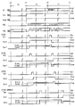
- Fig. 8 shows the operation waveforms when the liquid crystal display device is started up.
- FIG. 8 shows driving waveforms for each row from the start of power-on of the liquid crystal display device to the second frame.
- the control signal s0 becomes active at time t1, thereby causing each source output to the data signal output terminal of the source driver in each horizontal period.
- the auxiliary capacitor power supply potential Ecs and the common potential Vcom are raised by the power supply circuit.
- the first frame F1 is started at time t1.
- the display data written to the picture element PIX in the first row has a positive polarity in accordance with the data signal potential polarity POL, and the polarity of the display data is inverted one row at a time after the next row.
- the polarity of the display data written to the picture elements PIX in each row is inverted with respect to the polarity of the immediately preceding frame. Since the liquid crystal display device is normally black, black display data signal potential Vda is supplied to each pixel PIX as display data from the start of the display period to a predetermined frame.
- the pixel electrode 102 In the power-off state until time t0 when the apparatus power is turned on, the pixel electrode 102 is approximately at the GND potential via the output of the TFT 101 in the high impedance state, the source line SL, and the source driver in the high impedance state. Being Calm.
- the common potential Vcom rises at time t1 and the gate high potential Vgh is supplied as the scanning signal Vg1 to the gate line GL1 in the first row
- the data signal potential Vda (for example, 0. 2V) writing is started.
- the pixel electrode potential Vdr after the data signal potential Vda is written is lower than the rising common potential Vcom (for example, 2 V) as shown by V + (for example, 0.2 V) in FIG.
- the auxiliary capacitance potential Vcs1 applied to the auxiliary capacitance wiring CSL1 in the first row changes from the previous Low level (Vcsl) to the High level (Vcsh). Change.
- the pixel electrode potential Vdr1 is pushed up by ⁇ V + (for example, 2V) and becomes higher than the common potential Vcom as indicated by V + ′ (for example, 2.2V).
- V + ′ for example, 2.2V
- the next horizontal period starts, and when the gate high potential Vgh is supplied as the scanning signal Vg2 to the gate line GL2 in the second row, the data signal potential for black display of negative polarity is supplied to the pixel electrode 102.
- Vda for example, 3.8 V
- the pixel electrode potential Vdr after the writing of the data signal potential Vda is higher than the rising common potential Vcom (for example, 2V), as indicated by V ⁇ (for example, 3.8V) in FIG.
- the auxiliary capacitance potential Vcs1 applied to the auxiliary capacitance wiring CSL1 in the second row is changed to the low level (Vcsl:
- the odd-numbered picture element PIX is the same as the first-line picture element PIX, and the even-numbered picture element PIX is the second-line picture element.
- the data signal potential is written.
- the negative data signal potential Vda is written in the odd-numbered picture elements PIX.
- the positive data signal potential Vda is written into the picture elements PIX in the even-numbered rows.
- the auxiliary capacitance potential Vcs applied to the auxiliary capacitance wiring CSL is It changes from the previous High level (Vcsh) to the Low level (Vcsl).
- the pixel electrode potential Vdr is pushed down by ⁇ V ⁇ (for example, 2V) as shown in FIG. 7, and is lower than the common potential Vcom (for example, 2V) as indicated by V ⁇ ′ (for example, 1.8V).
- V ⁇ ′ for example, 1.8V.
- the auxiliary capacitance potential Vcs for pushing down the pixel electrode potential Vdr cannot change from the High level to the Low level.
- FIG. 9 a striped pattern composed of black display rows and gray display rows is displayed on the display screen of the first frame F1. This is visually a screen that flashes white for a moment, and the display quality deteriorates.
- Patent Document 1 discloses a technique for eliminating the horizontal streak at a time point before the first frame, but the striped pattern in the first frame cannot be eliminated.
- the conventional liquid crystal display device that drives the auxiliary capacitance wiring has a problem that the display quality is deteriorated when the device is started.
- the present invention has been made in view of the above-described conventional problems, and an object thereof is to realize a display device and a display device driving method capable of avoiding a reduction in display quality at the time of starting the device. .
- the display device of the present invention provides An active matrix type display device having an auxiliary capacity wiring for switching between a high level and a low level of an auxiliary capacity potential every frame,
- the common potential can be switched between a first common potential and a second common potential, and the first common potential is higher than the second common potential.
- the auxiliary capacitance potential starts from the low level.
- all the pixels in the same row have the same writing polarity with respect to the first common potential, and are written to the first common potential.
- the pixel electrode potential becomes the first potential during the selection period for the row of the pixel having a negative polarity for the first common potential.
- the first potential is set lower than the first common potential.
- the storage capacitor potential changes from the low level to the high level. Due to the change in the increase given to the auxiliary capacitance potential, the pixel electrode potential is pushed up to become the second potential. At this time, the second potential is lower than the first common potential.
- the potential difference between the pixel electrode potential and the first common potential at this time becomes a liquid crystal application voltage having a writing polarity having a negative polarity with respect to the first common potential, whereby the display of the first frame is performed.
- the pixel electrode potential becomes the third potential by the data signal potential supplied in the selection period.
- the third potential is set higher than the first common potential.
- the selection period ends, the storage capacitor potential continues to the previous Low level, so that the pixel electrode potential is not pushed down.
- the potential difference between the pixel electrode potential and the common potential at this time becomes a liquid crystal application voltage having a writing polarity having a positive polarity with respect to the first common potential, thereby displaying the first frame.
- the first common potential is set between the second potential and the third potential. Therefore, the liquid crystal applied voltage having a positive polarity with respect to the first common potential and the liquid crystal applied voltage having a negative polarity with respect to the first common potential are close to each other. Therefore, as in the prior art, the pixel electrode potential due to the data signal potential for one polarity is greatly separated from the common potential between the rows to which data signal potentials for different polarities are applied, with the same writing polarity. There is no.
- the display device driving method of the present invention provides: A driving method of a display device for driving an active matrix type display device having an auxiliary capacitance wiring for switching between a high level and a low level of an auxiliary capacitance potential every frame, The common potential is switched between a first common potential and a second common potential, and the first common potential is higher than the second common potential, In the first frame after the device power is turned on, the auxiliary capacitance potential starts from the low level. Using the first common potential as the common potential, all the pixels in the same row have the same writing polarity with respect to the first common potential, and are written to the first common potential.
- the pixel electrode potential becomes the first potential during the selection period for the row of the pixel having a negative polarity for the first common potential.
- the first potential is set lower than the first common potential.
- the storage capacitor potential changes from the low level to the high level. Due to the change in the increase given to the auxiliary capacitance potential, the pixel electrode potential is pushed up to become the second potential. At this time, the second potential is lower than the first common potential.
- the potential difference between the pixel electrode potential and the first common potential at this time becomes a liquid crystal application voltage having a writing polarity having a negative polarity with respect to the first common potential, whereby the display of the first frame is performed.
- the pixel electrode potential becomes the third potential by the data signal potential supplied in the selection period.
- the third potential is set higher than the first common potential.
- the selection period ends, the storage capacitor potential continues to the previous Low level, so that the pixel electrode potential is not pushed down.
- the potential difference between the pixel electrode potential and the common potential at this time becomes a liquid crystal application voltage having a writing polarity having a positive polarity with respect to the first common potential, thereby displaying the first frame.
- the first common potential is set between the second potential and the third potential. Therefore, the liquid crystal applied voltage having a positive polarity with respect to the first common potential and the liquid crystal applied voltage having a negative polarity with respect to the first common potential are close to each other. Therefore, as in the prior art, the pixel electrode potential due to the data signal potential for one polarity is greatly separated from the common potential between the rows to which data signal potentials for different polarities are applied, with the same writing polarity. There is no.
- the display device of the present invention is as described above.
- An active matrix type display device having an auxiliary capacity wiring for switching between a high level and a low level of an auxiliary capacity potential every frame,
- the common potential can be switched between a first common potential and a second common potential, and the first common potential is higher than the second common potential.
- the auxiliary capacitance potential starts from the low level.
- all the pixels in the same row have the same writing polarity with respect to the first common potential, and are written to the first common potential.
- the driving method of the display device of the present invention is as follows.
- a driving method of a display device for driving an active matrix type display device having an auxiliary capacitance wiring for switching between a high level and a low level of an auxiliary capacitance potential every frame The common potential is switched between a first common potential and a second common potential, and the first common potential is higher than the second common potential,
- the auxiliary capacitance potential starts from the low level.
- the first common potential as the common potential, all the pixels in the same row have the same writing polarity with respect to the first common potential, and are written to the first common potential.
- FIG. 3 is a waveform diagram illustrating the operation of the display device according to the embodiment of the present invention. It is a figure explaining the change of the pixel electrode potential by the operation
- FIG. It is a circuit diagram which shows the structure of the pixel with which the display apparatus of FIG. 1 is provided.
- FIG. 2 is a circuit diagram illustrating a connection relationship between a switch included in the display device of FIG. 1 and its periphery. It is a circuit diagram which shows a prior art and shows the structure of the pixel with which a display apparatus is provided. It is a figure explaining the change of the pixel electrode potential of the pixel of FIG. It is a wave form diagram explaining operation
- FIGS. 1 to 5 Embodiments of the present invention will be described with reference to FIGS. 1 to 5 as follows.
- FIG. 3 shows a configuration of a liquid crystal display device (display device) 1 according to the present embodiment.
- the liquid crystal display device 1 is an active matrix display device, and includes a display unit 2, a gate driver 3 as a scanning signal line driving circuit, a source driver 4 as a data signal line driving circuit, and an auxiliary capacitance wiring driving circuit 5. , A gate driver 3, a source driver 4, an auxiliary capacitance wiring drive circuit 5, and an external drive circuit 6 for driving and controlling the counter electrode COM.
- the liquid crystal display device 1 performs gate line inversion driving as AC driving. Further, the driving for inverting the polarity of the auxiliary capacitance potential Vcs applied to the auxiliary capacitance wiring CSL (described later) during the period in which the positive polarity data is supplied to the panel and the negative polarity data is supplied to the panel is assisted. This is performed for each capacitor wiring CSL.
- the display unit 2 includes a plurality of (m) data signal lines that intersect with each of the gate lines GL (GL1 to GLn) as a plurality of (n) scanning signal lines and the gate lines GL.
- Lines SL (SL1 to SLm) and a plurality (n ⁇ m) of picture elements PIX provided corresponding to the intersections of the gate lines GL and source lines SL, respectively.
- the display unit 2 includes auxiliary capacitance lines CSL (CSL1 to CSLn) in parallel with the gate lines GL, and includes m picture elements PIX arranged in the direction.
- One auxiliary capacitance line CSL is assigned to the picture element row.
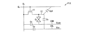
- the plurality of picture elements PIX are arranged in a matrix to form a picture element array, and each picture element PIX includes a TFT 11, a liquid crystal capacitor CL, and an auxiliary capacitor Cs as shown in FIG.
- the TFT 11 has a gate connected to the gate line GL, a source connected to the source line SL, and a drain connected to the pixel electrode 12.
- the liquid crystal capacitor CL is a capacitor in which a liquid crystal layer is disposed between the picture element electrode 12 and the counter electrode COM.
- the auxiliary capacitor Cs is a capacitor in which an insulating film is disposed between the pixel electrode 12 and the auxiliary capacitor line CSL.
- a common potential Vcom generated by a power supply circuit included in the external drive circuit 6 is applied to the counter electrode COM.
- This power supply circuit can switch and output a first common potential Vcom1 and a second common potential Vcom2, which will be described later, as the common potential Vcom.
- This switching can be realized, for example, by switching between the output of the first common potential Vcom1 and the output of the second common potential Vcom2 by a switch circuit and connecting to the common electrode COM.
- the auxiliary capacitance line CSL... Is generated from the high level voltage Vcsh and the low level voltage Vcsl generated by the power supply circuit included in the external drive circuit 6 and supplied to the auxiliary capacitance line drive circuit 5.
- the auxiliary capacitance potential Vcs generated for each auxiliary capacitance line CSL is applied.
- the voltage Vcsh and the voltage Vcsl are switched and applied to each auxiliary capacitance line CSL for each frame.
- the liquid crystal capacitor CL and the auxiliary capacitor Cs constitute a picture element capacity.
- a parasitic capacity Cgd formed between the picture element electrode 12 and the gate line GL is opposed to the pixel capacity.
- the parasitic capacitance Cx ⁇ Cy is also present in the conventional FIG.
- the external drive circuit 6 supplies the gate driver 3 with the gate clock signal GCK and the gate start pulse GSP and supplies the source driver 4 with the source in addition to supplying the above-described common potential Vcom and the auxiliary capacitor potential Vcs with voltages Vcsh and Vcsl.
- a clock signal SCK, a source start pulse SSP, and display data DA are supplied.
- source switches SW (SW1 to SW2) as switches are provided between the data signal output terminal of the source driver 4 and the source line SL.
- each source switch SW includes one data signal output terminal and a plurality of source lines SL such as RGB. And one provided between each of the two is simply shown.
- each horizontal RGB data signal forming one set is supplied to each source in a time division manner from one data signal output terminal assigned to each set through each source switch for branching. Output to line SL.
- the source switch SW is not necessarily required. For example, a configuration in which the output amplifier of the source driver 4 switches between a state where output is possible and a state where output is impossible is considered.
- the source switch SW is composed of, for example, a TFT, and is connected between the output of the output amplifier 4a of the source driver 4 and the source line SL.
- the ON / OFF control of the source switch SW is performed by a control signal s0 supplied from the external drive circuit 6.
- the source switch SW is typically built monolithically on the display panel.
- the source driver 4 is typically configured as an IC, but may be monolithically formed on the display panel. These forms are suitable for a panel using, for example, polycrystalline silicon, CG silicon, microcrystalline silicon, or the like.
- the source switch SW may be provided inside the source driver 4 configured as an IC, or may be provided outside the display panel. This form is suitable for a panel using amorphous silicon, for example.
- the source switch SW is not limited to the TFT, and any type of switch such as a general field effect transistor or bipolar transistor can be used.
- Fig. 1 shows the operation waveforms when the liquid crystal display device is started up.
- FIG. 1 shows driving waveforms for each gate line GL from the start of power-on to the second frame of the liquid crystal display device.
- the display period starts at time t1.
- the control signal s0 of the source switch SW becomes active (High level in this example).
- the source switch SW is driven ON / OFF by time-division driving. Become.
- the source output from the output stage of the source driver 4 becomes active.
- the first frame F1 is started at time t1.
- the display data to be written to the picture element PIX in the first row is the display data that becomes positive with respect to the common potential Vcom in the second frame F2 or later which is the normal operation period.
- the drive to invert the polarity of the display data one row at a time after the next row is performed.
- the normal operation period is a period during which a normal operation for displaying an image is performed.
- the picture element electrode 12 In the power-off state until the power is turned on, the picture element electrode 12 is approximately settled at the GND potential via the TFT 11 in the high impedance state, the source line SL, and the source switch SW or the source output in the high impedance state. ing.
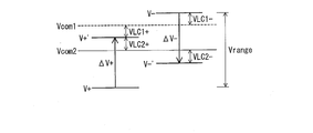
- the common potential Vcom in the first frame F1, is set to the first common potential Vcom1 that is higher than the second common potential Vcom2, which is a common potential in the second and subsequent frames.
- the auxiliary capacitance line CSL In the power-off state until the power is turned on, the auxiliary capacitance line CSL is also substantially at the GND potential (Low level), and the auxiliary capacitance potential Vcs starts from the Low level when the device is activated and in the first frame.
- a later-described first potential as the common potential Vcom is applied to the picture element electrode 12 in the normal operation period (after time t2).
- a data signal potential Vda for black display having a positive polarity with respect to the two common potential Vcom2 is supplied.
- the pixel electrode potential Vdr becomes the potential (first potential) V + by the data signal potential Vda supplied during the selection period.
- the potential V + is set lower than the first common potential Vcom1.
- the auxiliary capacitance potential Vcs1 applied to the auxiliary capacitance wiring CSL1 in the first row changes from the previous Low level (Vcsl) to the High level (Vcsh). And change. Due to the change in the increase applied to the auxiliary capacitance potential Vcs1, the pixel electrode potential Vdr1 is pushed up by ⁇ V + to become a potential (second potential) V + ′. At this time, the relationship between the first common potential Vcom1 and the auxiliary capacitance potential Vcs1 is set so that the potential V + 'is lower than the first common potential Vcom1.
- the potential difference Vcom1-V + ′ which is the absolute value of the difference between the pixel electrode potential Vdr1 and the first common potential Vcom1, becomes the liquid crystal application voltage VLC1 + of the black display level, whereby black display in the first row is performed.
- the liquid crystal applied voltage VLC1 + in the first row in the first frame F1 and thus in the odd-numbered row in the first frame F1, is black display data that is positive with respect to the second common potential Vcom2 in the normal operation period. Is used to obtain a negative polarity writing voltage with respect to the first common potential Vcom1.
- the process proceeds to the next horizontal period, and during the selection period of the picture element PIX in which the gate high potential Vgh is supplied as the scanning signal Vg2 to the gate line GL2 in the second row, the normal operation period is applied to the picture element electrode 12. Then, the black display data signal potential Vda having a negative polarity with respect to the second common potential Vcom is supplied. As shown in FIG. 2, the pixel electrode potential Vdr2 becomes the potential (third potential) V ⁇ by the data signal potential Vda supplied during the selection period. The potential V ⁇ is set higher than the first common potential Vcom1.
- the auxiliary capacitance potential Vcs2 applied to the auxiliary capacitance line CSL2 in the second row is not changed, and the auxiliary capacitance potential Vcs2 is low until then. Since the level (Vcsl: GND potential, for example) is continued, the picture element electrode potential Vdr2 is not subjected to the push-down. At this time, the potential difference (V ⁇ ) ⁇ Vcom1 that is the absolute value of the difference between the pixel electrode potential Vdr2 and the first common potential Vcom1 becomes the liquid crystal application voltage VLC1 ⁇ at the black display level, whereby black display in the second row is performed. Is done.
- the liquid crystal applied voltage VLC1- in the second row in the first frame F1, and thus in the even-numbered row in the first frame F1, is for black display that has a negative polarity with respect to the second common potential Vcom2 in the normal operation period.
- the odd-numbered picture element PIX is the same as the first-line picture element PIX, and the even-numbered picture element PIX is the second-line picture element. Similar to PIX, the pixel electrode potential Vdr is determined.
- the second frame F2 is started. Thereby, the normal operation period is started.
- the control signal s0 remains active.
- the common potential Vcom is set to the second common potential Vcom2.
- the black display data signal potential Vda is supplied to the pixel electrode 12.
- the pixel electrode potential Vdr becomes the potential V ⁇ by the data signal potential Vda supplied during the selection period.
- the pixel electrode potential Vdr1 Due to the change in increase applied to the auxiliary capacitance potential Vcs1, the pixel electrode potential Vdr1 is pushed down by ⁇ V ⁇ to become the potential (fourth potential) V ⁇ ′.
- the relationship between the second common potential Vcom2 and the auxiliary capacitance potential Vcs1 is set so that the potential V- 'is lower than the second common potential Vcom2.
- the potential difference Vcom2- (V ⁇ ′) which is the absolute value of the difference between the pixel electrode potential Vdr1 and the second common potential Vcom2, becomes the liquid crystal application voltage VLC2 ⁇ at the black display level. Display is performed.
- the liquid crystal applied voltage VLC2- in the first row in the second frame F2, and thus in the odd-numbered row in the second frame F2, is for black display having a negative polarity with respect to the second common potential Vcom in the normal operation period.
- the data is used as a voltage having a negative writing polarity with respect to the second common potential Vcom.
- the process proceeds to the next horizontal period, and during the selection period of the picture element PIX in which the gate high potential Vgh is supplied as the scanning signal Vg2 to the gate line GL2 in the second row, the pixel electrode 12 has positive polarity.
- the black display data signal potential Vda is supplied.
- the pixel electrode potential Vdr becomes the potential V + by the data signal potential Vda supplied during the selection period.
- the pixel electrode potential Vdr1 Due to the change in the increase applied to the auxiliary capacitance potential Vcs2, the pixel electrode potential Vdr1 is pushed up by ⁇ V + to become the potential V + ′.
- the relationship between the second common potential Vcom2 and the auxiliary capacitance potential Vcs2 is set so that the potential V + 'is higher than the second common potential Vcom2.
- the potential difference (V + ′) ⁇ Vcom2 which is the absolute value of the difference between the pixel electrode potential Vdr1 and the second common potential Vcom2, becomes the liquid crystal application voltage VLC2 + at the black display level, whereby the black display in the second row is performed. Done.
- the liquid crystal applied voltage VLC2 + in the second row in the second frame F2, and thus in the even-numbered row in the second frame F2, is black display data that is positive with respect to the second common potential Vcom in the normal operation period. Is used as a voltage having a positive polarity for the second common potential Vcom.
- the odd-numbered picture element PIX is the same as the first-line picture element PIX
- the even-numbered picture element PIX is the second-line picture element. Similar to PIX, the pixel electrode potential Vdr is determined. Further, after the third frame F3, the operation is performed on the same principle as that of the second frame F2, while inverting the polarity of the data signal da of each picture element with respect to the common potential Vcom of the own frame from that of the previous frame.
- the potential difference (V ⁇ ) ⁇ Vcom2 in FIG. 2 is typically a large value as described for the potential difference (V ⁇ ) ⁇ Vcom in FIG. 7, and the liquid crystal at the time of black display in FIG. It is sufficiently larger than the applied voltage VLC2 + and the liquid crystal applied voltage VLC2-.
- the liquid crystal applied voltage VLC1 + and the liquid crystal applied voltage VLC1- in the first frame F1 are smaller than the potential difference Vcom2- (V +) and the potential difference (V ⁇ ) ⁇ Vcom2, the liquid crystal applied voltage in the first frame F1 is positive.
- the black display voltage can be set smaller than the gray display voltage.
- the first common potential is defined between the potential V + ′ and the potential V ⁇ . Since the common potential is set, the liquid crystal application voltage having a positive writing polarity with respect to the first common potential and the liquid crystal application voltage having a negative writing polarity with respect to the first common potential are close to each other. Therefore, as in the prior art shown in FIG. 7, the liquid crystal application voltages in the odd and even rows have the same write polarity even though the data signal potentials for different polarities are given. The pixel electrode potential due to the data signal potential for one polarity is not greatly separated from the common potential.
- the display screen of the first frame F1 can avoid displaying a striped pattern composed of black display rows and gray display rows as shown in FIG.
- the value of the first common potential Vcom1 is set between the potential V + ′ and the potential V ⁇ .
- the liquid crystal applied voltage VLC1 + and the liquid crystal applied voltage VLC1- are equally close to the liquid crystal applied voltage VLC2 + and the liquid crystal applied voltage VLC2- for black display. Display can be made. In particular, in the case of normally black, black display is obtained when the liquid crystal applied voltage is below the threshold voltage.
- the liquid crystal applied voltages VLC2 +, VLC2 ⁇ can also correspond to the equivalent black display level. Further, if the liquid crystal applied voltages VLC2 + and VLC2- and the liquid crystal applied voltages VLC1 + and VLC1- are gray display levels other than the black display level, etc., if the inequality (1) holds, the liquid crystal applied voltages VLC2 + and VLC2- Since the liquid crystal applied voltages VLC1 + and VLC1- are close to each other, it is effective for displaying some constant color in a predetermined period after the apparatus is started.
- liquid crystal applied voltage VLC1 + and the liquid crystal applied voltage VLC1- do not necessarily have to be equal to each other as long as they are at a sufficient black display level, but are equal to each other between pixels having different polarities in the first frame F1. This is preferable in that the black display level is accurately aligned.
- the liquid crystal applied voltage VLC2 + and the liquid crystal applied voltage VLC2- do not necessarily have to be equal to each other, but the effective value of the positive polarity liquid crystal applied voltage and the effective value of the negative polarity liquid crystal applied voltage are equal to each other.
- display luminance is uniform between picture elements having different polarities in the same frame.
- the common potential Vcom is set to the first common potential Vcom1 in the first frame F1
- the data signal potential Vda to be used is the same as that in the normal operation period.
- the entire data signal potential range Vrange of the negative data signal potential range and the negative data signal potential need not be particularly widened.
- the conventional data signal potential range Vrange can be used as it is.
- the gate line inversion drive is performed.
- the present invention is not limited to this.
- the liquid crystal display device performs the AC drive in which the data signal potentials having the same polarity are written to all the picture elements PIX in the same row. It's okay.
- the display device of the present invention provides An active matrix type display device having an auxiliary capacity wiring for switching between a high level and a low level of an auxiliary capacity potential every frame,
- the common potential can be switched between a first common potential and a second common potential, and the first common potential is higher than the second common potential.
- the auxiliary capacitance potential starts from the low level.
- all the pixels in the same row have the same writing polarity with respect to the first common potential, and are written to the first common potential.
- the pixel electrode potential becomes the first potential during the selection period for the row of the pixel having the negative polarity for the first common potential.
- the first potential is set lower than the first common potential.
- the storage capacitor potential changes from the low level to the high level. Due to the change in the increase given to the auxiliary capacitance potential, the pixel electrode potential is pushed up to become the second potential. At this time, the second potential is lower than the first common potential.
- the potential difference between the pixel electrode potential and the first common potential at this time becomes a liquid crystal application voltage having a writing polarity of a negative polarity with respect to the first common potential, thereby displaying the first frame.
- the pixel electrode potential becomes the third potential by the data signal potential supplied in the selection period.
- the third potential is set higher than the first common potential.
- the selection period ends, the storage capacitor potential continues to the previous Low level, so that the pixel electrode potential is not pushed down.
- the potential difference between the pixel electrode potential and the common potential at this time becomes a liquid crystal application voltage having a writing polarity having a positive polarity with respect to the first common potential, thereby displaying the first frame.
- the first common potential is set between the second potential and the third potential. Therefore, the liquid crystal applied voltage having a positive polarity with respect to the first common potential and the liquid crystal applied voltage having a negative polarity with respect to the first common potential are close to each other. Therefore, as in the prior art, the pixel electrode potential due to the data signal potential for one polarity is greatly separated from the common potential between the rows to which data signal potentials for different polarities are applied, with the same writing polarity. There is no.
- the data signal supplied to the first frame is a data signal for black display.
- the above invention it is possible to avoid the occurrence of a striped pattern composed of black display rows and gray display rows when the apparatus is activated.
- black display is obtained when the liquid crystal applied voltage is equal to or lower than the threshold voltage. Therefore, the liquid crystal applied voltage due to the difference between the second potential and the first common potential, the third potential, and the first common are displayed. There is an effect that the liquid crystal applied voltage due to the difference from the potential can be easily made to correspond to the equivalent black display level.
- the display device of the present invention provides After the second frame,
- the second common potential is used as a common potential so that all picture elements in the same row have the same writing polarity with respect to the second common potential, and in the same frame, with respect to the second common potential.
- a data signal is supplied and AC driven so that there are rows of picture elements with different writing polarities, For a row of picture elements having a positive polarity for writing with respect to the second common potential, a data signal having the first potential is supplied, and a pixel writing period is set for the corresponding auxiliary capacitance wiring.
- the pixel electrode potential is changed to the second potential.
- a data signal of the third potential is supplied, and a picture element writing period is set for the corresponding auxiliary capacitance wiring.
- the pixel electrode potential is changed to a fourth potential lower than the second common potential by changing the auxiliary capacitance potential from the High level to the Low level.
- the same color display in the second and subsequent frames, the same color display can be performed using the data signal having the same first potential as that in the first frame and the third data signal. Therefore, there is an effect that it is not necessary to expand the range of the data signal potential when realizing the first frame with high display quality.
- the display device of the present invention provides The absolute value of the difference between the second potential and the first common potential is VLC1 +, the absolute value of the difference between the third potential and the first common potential is VLC1-, the second potential and the second potential. If the absolute value of the difference from the common potential is VLC2 +, and the absolute value of the difference between the fourth potential and the second common potential is VLC2- VLC2 +, VLC2- ⁇ VLC1 +, VLC1- ⁇ (Third potential)-(Second common potential) It is characterized by being.
- the liquid crystal applied voltage VLC1 + and the liquid crystal applied voltage VLC1- are equally close to the liquid crystal applied voltage VLC2 + and the liquid crystal applied voltage VLC2- for black display, and even more uniform black display is performed at startup.
- black display can be obtained when the applied voltage of the liquid crystal is lower than the threshold voltage. Therefore, VLC1 +, VLC1- ⁇ (third potential) ⁇ (second common potential).
- the applied voltages VLC2 + and VLC2- and the liquid crystal applied voltages VLC1 + and VLC1- both have the effect of corresponding to an equivalent black display level.
- the liquid crystal applied voltages VLC2 + and VLC2- and the liquid crystal applied voltages VLC1 + and VLC1- are set to gray display levels other than the black display level, the liquid crystal applied voltages VLC2 + and VLC2- and the liquid crystal applied Since the voltages VLC1 + and VLC1- are close to each other, there is an effect that the voltage VLC1 + and VLC1- are effective for displaying some constant color in a predetermined period after the apparatus is activated.
- the display device driving method of the present invention provides: A driving method of a display device for driving an active matrix type display device having an auxiliary capacitance wiring for switching between a high level and a low level of an auxiliary capacitance potential every frame, The common potential is switched between a first common potential and a second common potential, and the first common potential is higher than the second common potential, In the first frame after the device power is turned on, the auxiliary capacitance potential starts from the low level. Using the first common potential as the common potential, all the pixels in the same row have the same writing polarity with respect to the first common potential, and are written to the first common potential.
- the pixel electrode potential becomes the first potential during the selection period for the row of the pixel having a negative polarity for the first common potential.
- the first potential is set lower than the first common potential.
- the storage capacitor potential changes from the low level to the high level. Due to the change in the increase given to the auxiliary capacitance potential, the pixel electrode potential is pushed up to become the second potential. At this time, the second potential is lower than the first common potential.
- the potential difference between the pixel electrode potential and the first common potential at this time becomes a liquid crystal application voltage having a writing polarity having a negative polarity with respect to the first common potential, whereby the display of the first frame is performed.
- the pixel electrode potential becomes the third potential by the data signal potential supplied in the selection period.
- the third potential is set higher than the first common potential.
- the selection period ends, the storage capacitor potential continues to the previous Low level, so that the pixel electrode potential is not pushed down.
- the potential difference between the pixel electrode potential and the common potential at this time becomes a liquid crystal application voltage having a writing polarity having a positive polarity with respect to the first common potential, thereby displaying the first frame.
- the first common potential is set between the second potential and the third potential. Therefore, the liquid crystal applied voltage having a positive polarity with respect to the first common potential and the liquid crystal applied voltage having a negative polarity with respect to the first common potential are close to each other. Therefore, as in the prior art, the pixel electrode potential due to the data signal potential for one polarity is greatly separated from the common potential between the rows to which data signal potentials for different polarities are applied, with the same writing polarity. There is no.
- the display device driving method of the present invention provides:
- the data signal supplied to the first frame is a data signal for black display.
- the above invention it is possible to avoid the occurrence of a striped pattern composed of black display rows and gray display rows when the apparatus is activated.
- black display is obtained when the liquid crystal applied voltage is equal to or lower than the threshold voltage. Therefore, the liquid crystal applied voltage due to the difference between the second potential and the first common potential, the third potential, and the first common are displayed. There is an effect that the liquid crystal applied voltage due to the difference from the potential can be easily made to correspond to the equivalent black display level.
- the display device driving method of the present invention provides: After the second frame, The second common potential is used as a common potential so that all picture elements in the same row have the same writing polarity with respect to the second common potential, and in the same frame, with respect to the second common potential.
- a data signal is supplied and AC driven so that there are rows of picture elements with different writing polarities, For a row of picture elements having a positive polarity for writing with respect to the second common potential, a data signal having the first potential is supplied, and a pixel writing period is set for the corresponding auxiliary capacitance wiring.
- the pixel electrode potential is changed to the second potential.
- a data signal of the third potential is supplied, and a picture element writing period is set for the corresponding auxiliary capacitance wiring.
- the pixel electrode potential is changed to a fourth potential lower than the second common potential by changing the auxiliary capacitance potential from the High level to the Low level.
- the same color display in the second and subsequent frames, the same color display can be performed using the data signal having the same first potential as that in the first frame and the third data signal. Therefore, there is an effect that it is not necessary to expand the range of the data signal potential when realizing the first frame with high display quality.
- the display device driving method of the present invention provides: The absolute value of the difference between the second potential and the first common potential is VLC1 +, the absolute value of the difference between the third potential and the first common potential is VLC1-, the second potential and the second potential. If the absolute value of the difference from the common potential is VLC2 +, and the absolute value of the difference between the fourth potential and the second common potential is VLC2- VLC2 +, VLC2- ⁇ VLC1 +, VLC1- ⁇ (Third potential)-(Second common potential) It is characterized by being.
- the liquid crystal applied voltage VLC1 + and the liquid crystal applied voltage VLC1- are equally close to the liquid crystal applied voltage VLC2 + and the liquid crystal applied voltage VLC2- for black display, and even more uniform black display is performed at startup.
- black display can be obtained when the applied voltage of the liquid crystal is lower than the threshold voltage. Therefore, VLC1 +, VLC1- ⁇ (third potential) ⁇ (second common potential).
- the applied voltages VLC2 + and VLC2- and the liquid crystal applied voltages VLC1 + and VLC1- both have the effect of corresponding to an equivalent black display level.
- the liquid crystal applied voltages VLC2 + and VLC2- and the liquid crystal applied voltages VLC1 + and VLC1- are set to gray display levels other than the black display level, the liquid crystal applied voltages VLC2 + and VLC2- and the liquid crystal applied Since the voltages VLC1 + and VLC1- are close to each other, there is an effect that the voltage VLC1 + and VLC1- are effective for displaying some constant color in a predetermined period after the apparatus is activated.
- the present invention can be suitably used for various display devices including a liquid crystal display device.
- Liquid crystal display device (display device) CSL auxiliary capacitance wiring F1 first frame F2 second frame PIX picture element Vcom common potential Vcom1 first common potential Vcom2 second common potential Vdr pixel electrode potential Vcs auxiliary capacitance potential V + potential (first potential) V + 'potential (second potential) V- potential (third potential) V- 'potential (fourth potential)
Landscapes
- Engineering & Computer Science (AREA)
- Chemical & Material Sciences (AREA)
- Crystallography & Structural Chemistry (AREA)
- Physics & Mathematics (AREA)
- Computer Hardware Design (AREA)
- General Physics & Mathematics (AREA)
- Theoretical Computer Science (AREA)
- Control Of Indicators Other Than Cathode Ray Tubes (AREA)
- Liquid Crystal Display Device Control (AREA)
- Liquid Crystal (AREA)
Abstract
La présente invention concerne un appareil d'affichage, un câblage de capacité auxiliaire étant commandé. Dans l'appareil d'affichage, dans la première trame (F1) après une mise sous tension, un premier potentiel commun (Vcom1) qui est supérieur à un second potentiel commun (Vcom2) est utilisé pour amener tous les pixels de la même rangée à montrer la même polarité d'écriture, tout en amenant des rangées dont les pixels montrent des polarités d'écritures différentes à exister ; pour les rangées montrant une polarité d'écriture négative, un signal de données, dont un premier potentiel (V+) est inférieur au premier potentiel commun (Vcom1), est émis pour amener un potentiel de capacité auxiliaire (Vcs1) à passer de Bas (Vcsl) à Haut (Vcsh), tout en amenant un potentiel d'électrode de pixel (Vdr1) à passer à un deuxième potentiel (V+') supérieur au second potentiel commun (Vcom2) et inférieur au premier potentiel commun (Vcom1) après la fin d'une période sélectionnée ; et pour les rangées montrant une polarité d'écriture positive, un signal de données, dont un troisième potentiel (V–) est supérieur au premier potentiel commun (Vcom1), est émis pour amener le potentiel de capacité auxiliaire (Vcs1) à rester Bas (Vcsl) après la fin de la période sélectionnée. Selon la présente invention, la dégradation d'une qualité d'affichage pendant l'activation d'appareils d'affichage à cristaux liquides peut être évitée.
Priority Applications (1)
| Application Number | Priority Date | Filing Date | Title |
|---|---|---|---|
| US13/376,415 US8698788B2 (en) | 2009-06-09 | 2010-05-18 | Display apparatus and display apparatus driving method |
Applications Claiming Priority (2)
| Application Number | Priority Date | Filing Date | Title |
|---|---|---|---|
| JP2009138559 | 2009-06-09 | ||
| JP2009-138559 | 2009-06-09 |
Publications (1)
| Publication Number | Publication Date |
|---|---|
| WO2010143501A1 true WO2010143501A1 (fr) | 2010-12-16 |
Family
ID=43308760
Family Applications (1)
| Application Number | Title | Priority Date | Filing Date |
|---|---|---|---|
| PCT/JP2010/058389 WO2010143501A1 (fr) | 2009-06-09 | 2010-05-18 | Appareil d'affichage et procédé de commande d'un appareil d'affichage |
Country Status (2)
| Country | Link |
|---|---|
| US (1) | US8698788B2 (fr) |
| WO (1) | WO2010143501A1 (fr) |
Citations (6)
| Publication number | Priority date | Publication date | Assignee | Title |
|---|---|---|---|---|
| JP2003295157A (ja) * | 2002-03-29 | 2003-10-15 | Matsushita Electric Ind Co Ltd | 液晶表示装置 |
| JP2007052290A (ja) * | 2005-08-18 | 2007-03-01 | Sony Corp | 表示装置およびその駆動方法 |
| JP2008015478A (ja) * | 2006-06-06 | 2008-01-24 | Epson Imaging Devices Corp | 電気光学装置、駆動回路および電子機器 |
| JP2008145837A (ja) * | 2006-12-12 | 2008-06-26 | Sharp Corp | 液晶表示装置 |
| JP2009086170A (ja) * | 2007-09-28 | 2009-04-23 | Epson Imaging Devices Corp | 電気光学装置及び電気光学装置の駆動方法並びに電子機器 |
| WO2009128281A1 (fr) * | 2008-04-16 | 2009-10-22 | シャープ株式会社 | Circuit de pilotage d'un appareil d'affichage à cristaux liquides |
Family Cites Families (6)
| Publication number | Priority date | Publication date | Assignee | Title |
|---|---|---|---|---|
| KR100608191B1 (ko) | 2003-07-11 | 2006-08-08 | 도시바 마쯔시따 디스플레이 테크놀로지 컴퍼니, 리미티드 | 액정 표시 장치 |
| JP2005049849A (ja) | 2003-07-11 | 2005-02-24 | Toshiba Matsushita Display Technology Co Ltd | 表示装置 |
| JP2006154088A (ja) * | 2004-11-26 | 2006-06-15 | Sanyo Electric Co Ltd | アクティブマトリクス型液晶表示装置 |
| US8866717B2 (en) | 2005-08-18 | 2014-10-21 | Japan Display, Inc. | Display device and drive method providing improved signal linearity |
| US7928941B2 (en) | 2007-03-20 | 2011-04-19 | Sony Corporation | Electro-optical device, driving circuit and electronic apparatus |
| JP4631917B2 (ja) * | 2008-02-29 | 2011-02-16 | エプソンイメージングデバイス株式会社 | 電気光学装置、駆動方法および電子機器 |
-
2010
- 2010-05-18 WO PCT/JP2010/058389 patent/WO2010143501A1/fr active Application Filing
- 2010-05-18 US US13/376,415 patent/US8698788B2/en not_active Expired - Fee Related
Patent Citations (6)
| Publication number | Priority date | Publication date | Assignee | Title |
|---|---|---|---|---|
| JP2003295157A (ja) * | 2002-03-29 | 2003-10-15 | Matsushita Electric Ind Co Ltd | 液晶表示装置 |
| JP2007052290A (ja) * | 2005-08-18 | 2007-03-01 | Sony Corp | 表示装置およびその駆動方法 |
| JP2008015478A (ja) * | 2006-06-06 | 2008-01-24 | Epson Imaging Devices Corp | 電気光学装置、駆動回路および電子機器 |
| JP2008145837A (ja) * | 2006-12-12 | 2008-06-26 | Sharp Corp | 液晶表示装置 |
| JP2009086170A (ja) * | 2007-09-28 | 2009-04-23 | Epson Imaging Devices Corp | 電気光学装置及び電気光学装置の駆動方法並びに電子機器 |
| WO2009128281A1 (fr) * | 2008-04-16 | 2009-10-22 | シャープ株式会社 | Circuit de pilotage d'un appareil d'affichage à cristaux liquides |
Also Published As
| Publication number | Publication date |
|---|---|
| US20120086688A1 (en) | 2012-04-12 |
| US8698788B2 (en) | 2014-04-15 |
Similar Documents
| Publication | Publication Date | Title |
|---|---|---|
| US8344991B2 (en) | Display device and driving method thereof | |
| US8749469B2 (en) | Display device for reducing parasitic capacitance with a dummy scan line | |
| JP5351974B2 (ja) | 表示装置 | |
| JP5346381B2 (ja) | 画素回路及び表示装置 | |
| KR101285054B1 (ko) | 액정표시장치 | |
| JP5346380B2 (ja) | 画素回路及び表示装置 | |
| US10049634B2 (en) | Pixel circuit and driving method thereof, driving circuit, display device | |
| JP4510530B2 (ja) | 液晶表示装置とその駆動方法 | |
| JP2005532590A (ja) | 液晶表示装置及びその駆動方法 | |
| JP4982349B2 (ja) | 液晶表示装置及びその駆動方法 | |
| US20160071493A1 (en) | Display device and display method thereof for compensating pixel voltage loss | |
| JP4639702B2 (ja) | 液晶表示装置及び液晶表示装置の駆動方法 | |
| JP5244352B2 (ja) | 表示装置及びそのストレージ駆動回路 | |
| JP2002099256A (ja) | 平面表示装置 | |
| KR101186018B1 (ko) | 액정표시장치 및 그의 구동 방법 | |
| JP2008233283A (ja) | 液晶表示装置およびその駆動方法 | |
| WO2009128281A1 (fr) | Circuit de pilotage d'un appareil d'affichage à cristaux liquides | |
| JP5418388B2 (ja) | 液晶表示装置 | |
| WO2010143501A1 (fr) | Appareil d'affichage et procédé de commande d'un appareil d'affichage | |
| JP2009069626A (ja) | 液晶表示装置およびその駆動方法 | |
| KR100309924B1 (ko) | 액정표시장치및액정표시장치의구동방법 | |
| JP2006171041A (ja) | 表示装置ならびにその駆動回路および駆動方法 | |
| JP2010217582A (ja) | 表示装置および表示装置の駆動方法 | |
| JP2006106019A (ja) | 液晶表示装置及び液晶表示装置の駆動制御方法 | |
| KR101232583B1 (ko) | 액정표시소자 및 그의 구동 방법 |
Legal Events
| Date | Code | Title | Description |
|---|---|---|---|
| 121 | Ep: the epo has been informed by wipo that ep was designated in this application |
Ref document number: 10786032 Country of ref document: EP Kind code of ref document: A1 |
|
| WWE | Wipo information: entry into national phase |
Ref document number: 13376415 Country of ref document: US |
|
| NENP | Non-entry into the national phase |
Ref country code: DE |
|
| 122 | Ep: pct application non-entry in european phase |
Ref document number: 10786032 Country of ref document: EP Kind code of ref document: A1 |
|
| NENP | Non-entry into the national phase |
Ref country code: JP |