WO2010140529A1 - シリコン酸化膜用成膜原料およびそれを用いたシリコン酸化膜の成膜方法 - Google Patents
シリコン酸化膜用成膜原料およびそれを用いたシリコン酸化膜の成膜方法 Download PDFInfo
- Publication number
- WO2010140529A1 WO2010140529A1 PCT/JP2010/058984 JP2010058984W WO2010140529A1 WO 2010140529 A1 WO2010140529 A1 WO 2010140529A1 JP 2010058984 W JP2010058984 W JP 2010058984W WO 2010140529 A1 WO2010140529 A1 WO 2010140529A1
- Authority
- WO
- WIPO (PCT)
- Prior art keywords
- oxide film
- silicon oxide
- film
- raw material
- forming
- Prior art date
- Legal status (The legal status is an assumption and is not a legal conclusion. Google has not performed a legal analysis and makes no representation as to the accuracy of the status listed.)
- Ceased
Links
Images


Classifications
-
- C—CHEMISTRY; METALLURGY
- C23—COATING METALLIC MATERIAL; COATING MATERIAL WITH METALLIC MATERIAL; CHEMICAL SURFACE TREATMENT; DIFFUSION TREATMENT OF METALLIC MATERIAL; COATING BY VACUUM EVAPORATION, BY SPUTTERING, BY ION IMPLANTATION OR BY CHEMICAL VAPOUR DEPOSITION, IN GENERAL; INHIBITING CORROSION OF METALLIC MATERIAL OR INCRUSTATION IN GENERAL
- C23C—COATING METALLIC MATERIAL; COATING MATERIAL WITH METALLIC MATERIAL; SURFACE TREATMENT OF METALLIC MATERIAL BY DIFFUSION INTO THE SURFACE, BY CHEMICAL CONVERSION OR SUBSTITUTION; COATING BY VACUUM EVAPORATION, BY SPUTTERING, BY ION IMPLANTATION OR BY CHEMICAL VAPOUR DEPOSITION, IN GENERAL
- C23C16/00—Chemical coating by decomposition of gaseous compounds, without leaving reaction products of surface material in the coating, i.e. chemical vapour deposition [CVD] processes
- C23C16/22—Chemical coating by decomposition of gaseous compounds, without leaving reaction products of surface material in the coating, i.e. chemical vapour deposition [CVD] processes characterised by the deposition of inorganic material, other than metallic material
- C23C16/30—Deposition of compounds, mixtures or solid solutions, e.g. borides, carbides, nitrides
- C23C16/40—Oxides
- C23C16/401—Oxides containing silicon
- C23C16/402—Silicon dioxide
-
- C—CHEMISTRY; METALLURGY
- C23—COATING METALLIC MATERIAL; COATING MATERIAL WITH METALLIC MATERIAL; CHEMICAL SURFACE TREATMENT; DIFFUSION TREATMENT OF METALLIC MATERIAL; COATING BY VACUUM EVAPORATION, BY SPUTTERING, BY ION IMPLANTATION OR BY CHEMICAL VAPOUR DEPOSITION, IN GENERAL; INHIBITING CORROSION OF METALLIC MATERIAL OR INCRUSTATION IN GENERAL
- C23C—COATING METALLIC MATERIAL; COATING MATERIAL WITH METALLIC MATERIAL; SURFACE TREATMENT OF METALLIC MATERIAL BY DIFFUSION INTO THE SURFACE, BY CHEMICAL CONVERSION OR SUBSTITUTION; COATING BY VACUUM EVAPORATION, BY SPUTTERING, BY ION IMPLANTATION OR BY CHEMICAL VAPOUR DEPOSITION, IN GENERAL
- C23C16/00—Chemical coating by decomposition of gaseous compounds, without leaving reaction products of surface material in the coating, i.e. chemical vapour deposition [CVD] processes
- C23C16/04—Coating on selected surface areas, e.g. using masks
- C23C16/045—Coating cavities or hollow spaces, e.g. interior of tubes; Infiltration of porous substrates
-
- C—CHEMISTRY; METALLURGY
- C23—COATING METALLIC MATERIAL; COATING MATERIAL WITH METALLIC MATERIAL; CHEMICAL SURFACE TREATMENT; DIFFUSION TREATMENT OF METALLIC MATERIAL; COATING BY VACUUM EVAPORATION, BY SPUTTERING, BY ION IMPLANTATION OR BY CHEMICAL VAPOUR DEPOSITION, IN GENERAL; INHIBITING CORROSION OF METALLIC MATERIAL OR INCRUSTATION IN GENERAL
- C23C—COATING METALLIC MATERIAL; COATING MATERIAL WITH METALLIC MATERIAL; SURFACE TREATMENT OF METALLIC MATERIAL BY DIFFUSION INTO THE SURFACE, BY CHEMICAL CONVERSION OR SUBSTITUTION; COATING BY VACUUM EVAPORATION, BY SPUTTERING, BY ION IMPLANTATION OR BY CHEMICAL VAPOUR DEPOSITION, IN GENERAL
- C23C16/00—Chemical coating by decomposition of gaseous compounds, without leaving reaction products of surface material in the coating, i.e. chemical vapour deposition [CVD] processes
- C23C16/22—Chemical coating by decomposition of gaseous compounds, without leaving reaction products of surface material in the coating, i.e. chemical vapour deposition [CVD] processes characterised by the deposition of inorganic material, other than metallic material
- C23C16/30—Deposition of compounds, mixtures or solid solutions, e.g. borides, carbides, nitrides
- C23C16/40—Oxides
- C23C16/401—Oxides containing silicon
-
- H—ELECTRICITY
- H10—SEMICONDUCTOR DEVICES; ELECTRIC SOLID-STATE DEVICES NOT OTHERWISE PROVIDED FOR
- H10P—GENERIC PROCESSES OR APPARATUS FOR THE MANUFACTURE OR TREATMENT OF DEVICES COVERED BY CLASS H10
- H10P14/00—Formation of materials, e.g. in the shape of layers or pillars
- H10P14/60—Formation of materials, e.g. in the shape of layers or pillars of insulating materials
- H10P14/63—Formation of materials, e.g. in the shape of layers or pillars of insulating materials characterised by the formation processes
- H10P14/6326—Deposition processes
- H10P14/6328—Deposition from the gas or vapour phase
- H10P14/6334—Deposition from the gas or vapour phase using decomposition or reaction of gaseous or vapour phase compounds, i.e. chemical vapour deposition
-
- H—ELECTRICITY
- H10—SEMICONDUCTOR DEVICES; ELECTRIC SOLID-STATE DEVICES NOT OTHERWISE PROVIDED FOR
- H10P—GENERIC PROCESSES OR APPARATUS FOR THE MANUFACTURE OR TREATMENT OF DEVICES COVERED BY CLASS H10
- H10P14/00—Formation of materials, e.g. in the shape of layers or pillars
- H10P14/60—Formation of materials, e.g. in the shape of layers or pillars of insulating materials
- H10P14/63—Formation of materials, e.g. in the shape of layers or pillars of insulating materials characterised by the formation processes
- H10P14/6326—Deposition processes
- H10P14/6328—Deposition from the gas or vapour phase
- H10P14/6334—Deposition from the gas or vapour phase using decomposition or reaction of gaseous or vapour phase compounds, i.e. chemical vapour deposition
- H10P14/6336—Deposition from the gas or vapour phase using decomposition or reaction of gaseous or vapour phase compounds, i.e. chemical vapour deposition in the presence of a plasma [PECVD]
-
- H—ELECTRICITY
- H10—SEMICONDUCTOR DEVICES; ELECTRIC SOLID-STATE DEVICES NOT OTHERWISE PROVIDED FOR
- H10P—GENERIC PROCESSES OR APPARATUS FOR THE MANUFACTURE OR TREATMENT OF DEVICES COVERED BY CLASS H10
- H10P14/00—Formation of materials, e.g. in the shape of layers or pillars
- H10P14/60—Formation of materials, e.g. in the shape of layers or pillars of insulating materials
- H10P14/66—Formation of materials, e.g. in the shape of layers or pillars of insulating materials characterised by the type of materials
- H10P14/668—Formation of materials, e.g. in the shape of layers or pillars of insulating materials characterised by the type of materials the materials being characterised by the deposition precursor materials
- H10P14/6681—Formation of materials, e.g. in the shape of layers or pillars of insulating materials characterised by the type of materials the materials being characterised by the deposition precursor materials the precursor containing a compound comprising Si
- H10P14/6684—Formation of materials, e.g. in the shape of layers or pillars of insulating materials characterised by the type of materials the materials being characterised by the deposition precursor materials the precursor containing a compound comprising Si the compound comprising silicon and oxygen
- H10P14/6686—Formation of materials, e.g. in the shape of layers or pillars of insulating materials characterised by the type of materials the materials being characterised by the deposition precursor materials the precursor containing a compound comprising Si the compound comprising silicon and oxygen the compound being a molecule comprising at least one silicon-oxygen bond and the compound having hydrogen or an organic group attached to the silicon or oxygen, e.g. a siloxane
-
- H—ELECTRICITY
- H10—SEMICONDUCTOR DEVICES; ELECTRIC SOLID-STATE DEVICES NOT OTHERWISE PROVIDED FOR
- H10P—GENERIC PROCESSES OR APPARATUS FOR THE MANUFACTURE OR TREATMENT OF DEVICES COVERED BY CLASS H10
- H10P14/00—Formation of materials, e.g. in the shape of layers or pillars
- H10P14/60—Formation of materials, e.g. in the shape of layers or pillars of insulating materials
- H10P14/69—Inorganic materials
- H10P14/692—Inorganic materials composed of oxides, glassy oxides or oxide-based glasses
- H10P14/6921—Inorganic materials composed of oxides, glassy oxides or oxide-based glasses containing silicon
- H10P14/6922—Inorganic materials composed of oxides, glassy oxides or oxide-based glasses containing silicon the material containing Si, O and at least one of H, N, C, F or other non-metal elements, e.g. SiOC, SiOC:H or SiONC
Definitions
- the present invention relates to a silicon oxide film forming material for forming a silicon oxide film on a substrate by a chemical vapor deposition (CVD) method and a silicon oxide film forming method using the same.
- CVD chemical vapor deposition
- silicon oxide films are frequently used as interlayer insulation films.
- a method of forming such a silicon oxide film a method of forming a film by CVD using TEOS (tetraethyl orthosilicate) which is an organosilane gas and an oxidizing agent is known.
- TEOS tetraethyl orthosilicate
- a silicon oxide film having a good film quality has been formed by plasma CVD using TEOS, and in particular, a film quality equivalent to a thermal oxide film has been obtained by microwave plasma CVD. For this reason, application of such a technique to a gate insulating film, which has been difficult to apply by conventional CVD, is also being studied.
- Patent Document 1 places an object to be processed in a processing container, and TEOS gas in the processing container.
- TEOS gas By introducing oxygen gas and hydrogen gas and heating the inside of the processing vessel at a temperature lower than the decomposition temperature of the TEOS gas in a reduced pressure atmosphere, the TEOS gas is treated while suppressing decomposition of the TEOS gas in the gas phase.
- a method of forming a silicon oxide film by adsorbing on a body and then decomposing the adsorbed TEOS has been proposed.
- TEOS is inherently easy to adhere because the CC bond existing therein is easily broken and active dangling bonds are likely to remain. For this reason, even if the method as shown in the above-mentioned patent document 1 is taken, there is a limit to the improvement of step coverage. Therefore, there is a demand for a film forming material that can form a silicon oxide film with better step coverage by the CVD method.
- An object of the present invention is to provide a film forming material for a silicon oxide film capable of obtaining good step coverage when a silicon oxide film is formed on a substrate by a CVD method, and a method for forming a silicon oxide film using the same. It is to provide.
- a film forming raw material for a silicon oxide film for forming a silicon oxide film on a substrate by chemical vapor deposition comprising a siloxane-based compound having a carbonyl group, and having an energy of By being applied, it is decomposed and CO is desorbed, and a product free from dangling bonds in the chemical structure is generated, and a film forming raw material for silicon oxide film that contributes to film formation is provided.
- a film having a structure in which a carbonyl group is incorporated into a part of the skeleton of the cyclic siloxane can be used as the film forming raw material for the silicon oxide film.
- it may have a structure in which a part of Si constituting the cyclic siloxane is substituted with a carbonyl group, or a part of O that constitutes the cyclic siloxane may be substituted with a carbonyl group.
- a substrate to be processed is disposed in a processing container, the silicon oxide film forming raw material and the oxidizing agent of the first aspect are introduced into the processing container, and the silicon Oxidation of products and oxides that contribute to deposition without chemical dangling bonds due to the chemical structure generated when CO is desorbed by applying energy to the film-forming raw material for oxide film and attached to the film-forming surface.
- a silicon oxide film forming method for forming a silicon oxide film on a substrate to be processed by reaction with an agent.
- the energy can be applied by generating plasma in the processing container.
- the plasma is preferably generated by microwaves.
- the plasma is preferably formed by microwaves radiated from a planar antenna.
- FIG. 3 is a schematic diagram showing a state where CO is desorbed from the film forming raw material for the silicon oxide film of FIG. 2. It is a figure for demonstrating an example of the manufacturing method of the film-forming raw material for silicon oxide films of this invention. It is sectional drawing which shows the RLSA microwave plasma processing apparatus for enforcing the silicon oxide film forming method of this invention.
- the film forming material for silicon oxide film according to the present invention is for forming a silicon oxide film on a substrate by chemical vapor deposition (CVD).
- a substrate to be processed is placed in a processing container, a film forming material gas for silicon oxide film and an oxidizing agent (for example, O 2 ) are supplied into the processing container, and energy is applied to form a silicon oxide film.
- the film raw material is decomposed to form a silicon oxide film on the substrate.
- the CVD may be thermal CVD in which the silicon oxide film forming raw material gas is decomposed by thermal energy, but from the viewpoint of obtaining good film quality, plasma CVD in which the silicon oxide film forming raw material is decomposed by plasma energy is preferable.
- plasma CVDs microwave plasma CVD is preferable because a high plasma density can be obtained at a low electron temperature.
- a siloxane-based compound having a carbonyl group is decomposed by application of energy, so that CO is desorbed, and a product in which no dangling bond exists in the chemical structure is generated.
- a product that contributes to film formation is used.
- the adhesion coefficient of the product generated by desorption of CO, which contributes to the film formation is low, and it enters the inside of the recess 2 having a high aspect ratio.
- a silicon oxide film can be formed with step coverage.
- the adhesion coefficient ⁇ is required to be 2.5 ⁇ 10 ⁇ 4 or less in calculation.
- the CC bond is preferentially broken by the application of energy, and an active dangling bond remains, so that the adhesion coefficient is large, and it is necessary for a recess having an aspect ratio of 10.
- ⁇ ⁇ 2.5 ⁇ 10 ⁇ 4 cannot be satisfied at all.
- dangling bonds remain in the product simply by desorbing CO and covering the inner wall surface of the recess, and when no dangling bonds exist in the decomposition product without desorption of CO.
- the adhesion coefficient can be reduced to some extent, it is difficult to satisfy ⁇ ⁇ 2.5 ⁇ 10 ⁇ 4 .
- a low adhesion coefficient is achieved and an aspect ratio of 10 or more is good due to both the surface blocking effect by CO and the effect that the product after CO desorption is stable.
- a silicon oxide film can be formed with a good step coverage.
- the compound constituting the raw material for forming a silicon oxide film according to the present invention include a structure in which a carbonyl group is included in a part of the skeleton of a cyclic siloxane.
- a structure in which part of O of the cyclic siloxane is substituted with a carbonyl group can be used.
- R shows alkyl groups, such as a methyl group, an ethyl group, a propyl group, and a butyl group.
- the alkyl group preferably has 1 to 4 carbon atoms.
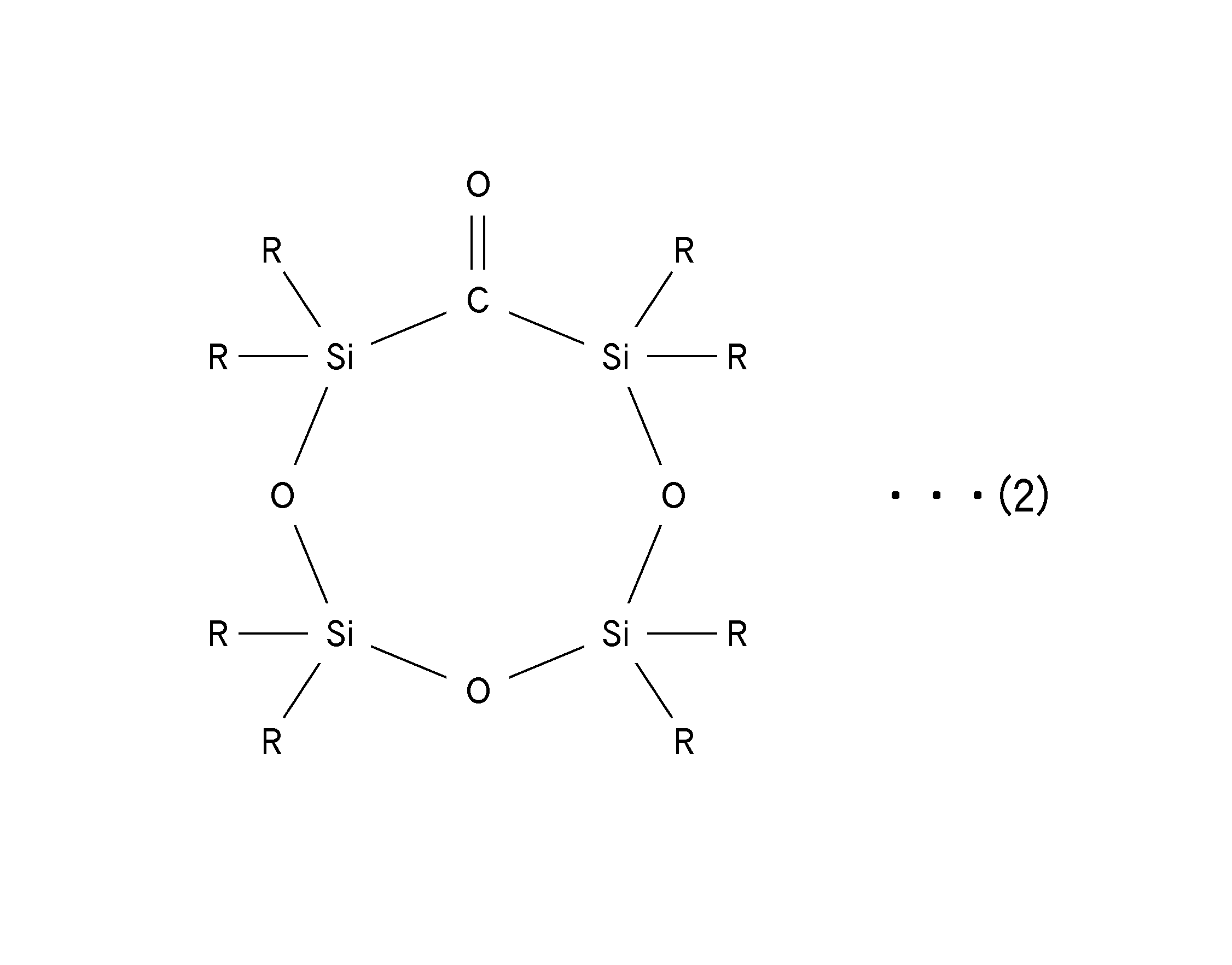
- the cyclic skeleton is an example of a trimer, but may be a tetramer or more.
- An example of a tetramer is shown in the following structural formula (2).
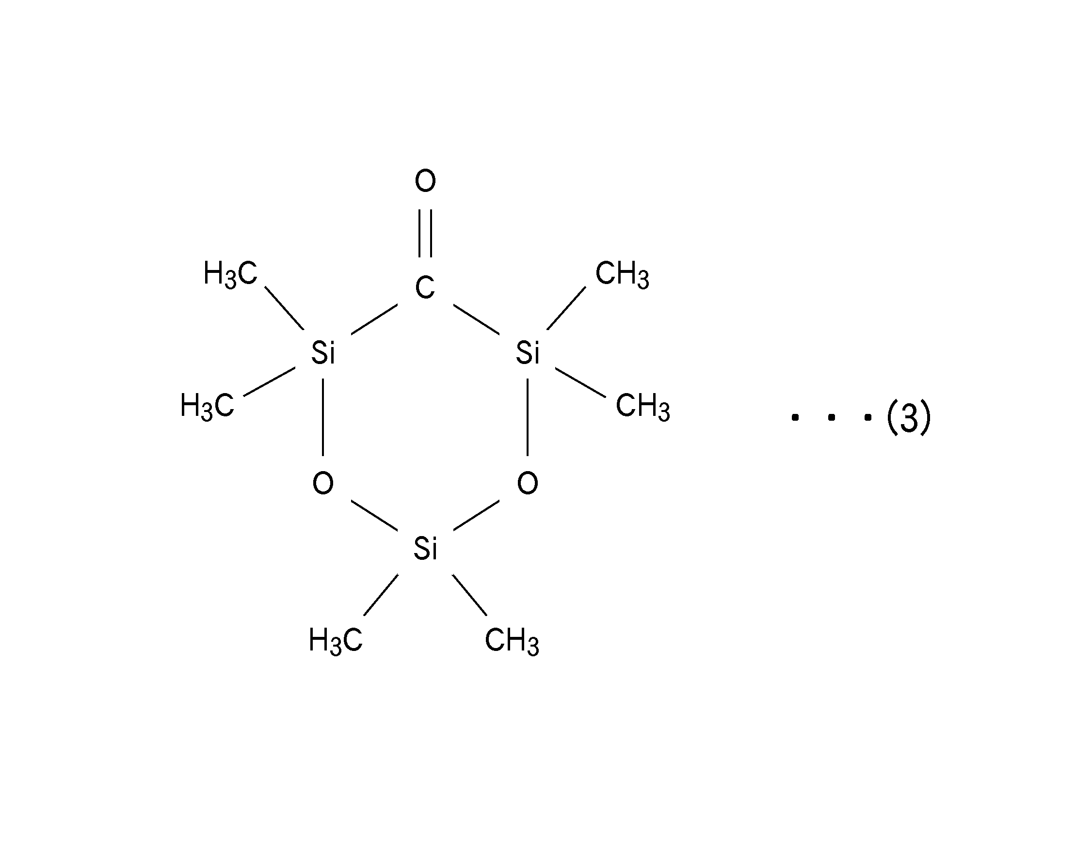
- the compound in which R is a methyl group is represented by the following structural formula (3).
- the binding energy of each bond of the compound of structural formula (3) is shown in FIG.
- the bond energy of Si and carbonyl group C is 3.0 eV
- the bond energy of Si and O is 4.6 eV
- the bond energy of Si and methyl group C is 3.3 eV
- the bond energy of H and H is 4.2 eV. Therefore, the bond between Si having the smallest bond energy and C of the carbonyl group is easily broken, and CO is desorbed preferentially as shown in FIG.
- the product after elimination becomes a stable compound having no dangling bond in terms of chemical structure, as shown in the following structural formula (4).
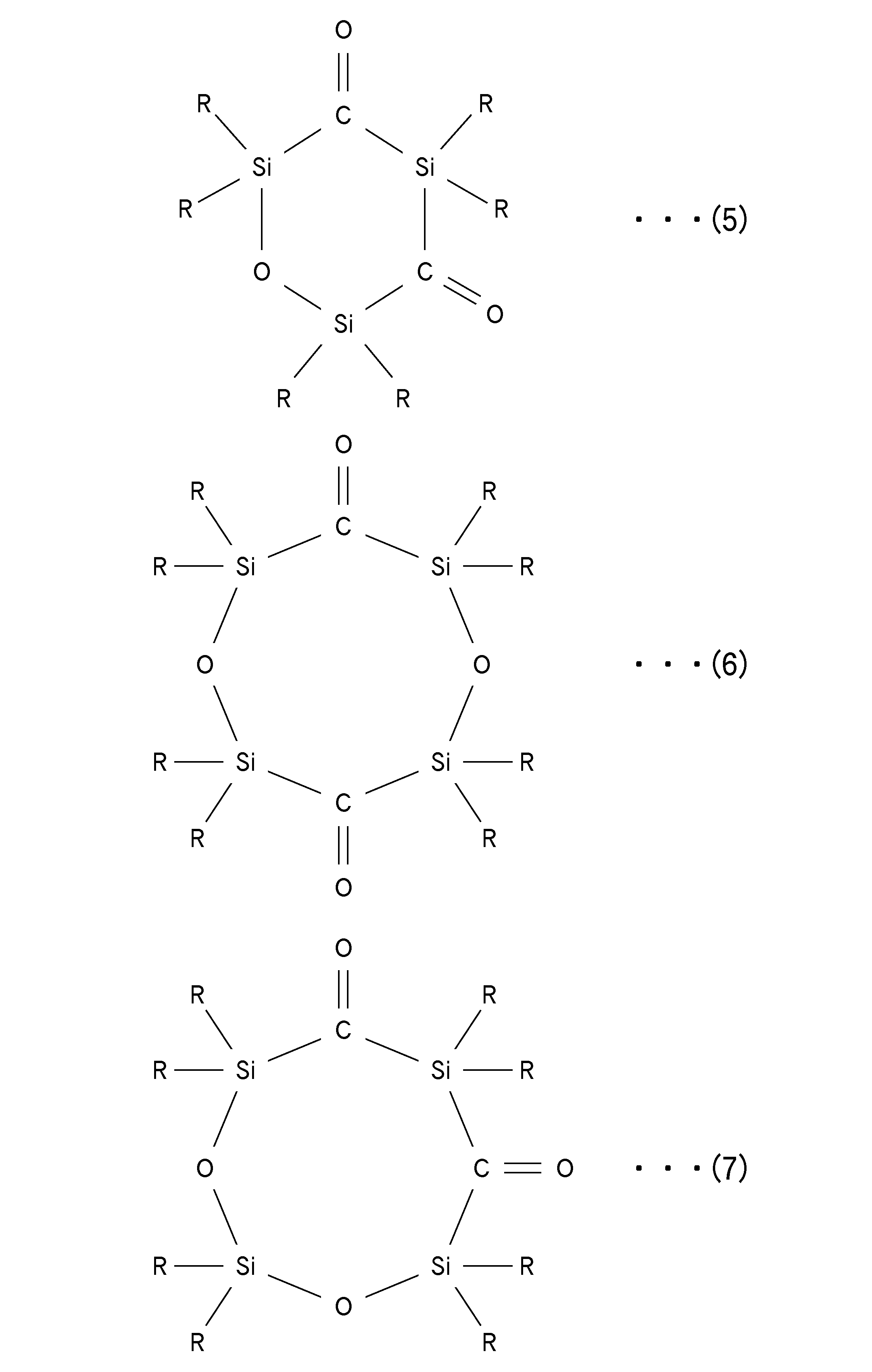
- the number of carbonyl groups is not limited to one per molecule of the compound constituting the film forming raw material, and may be two as shown in the following structural formulas (5), (6), and (7), for example, 3 It may be more than one.
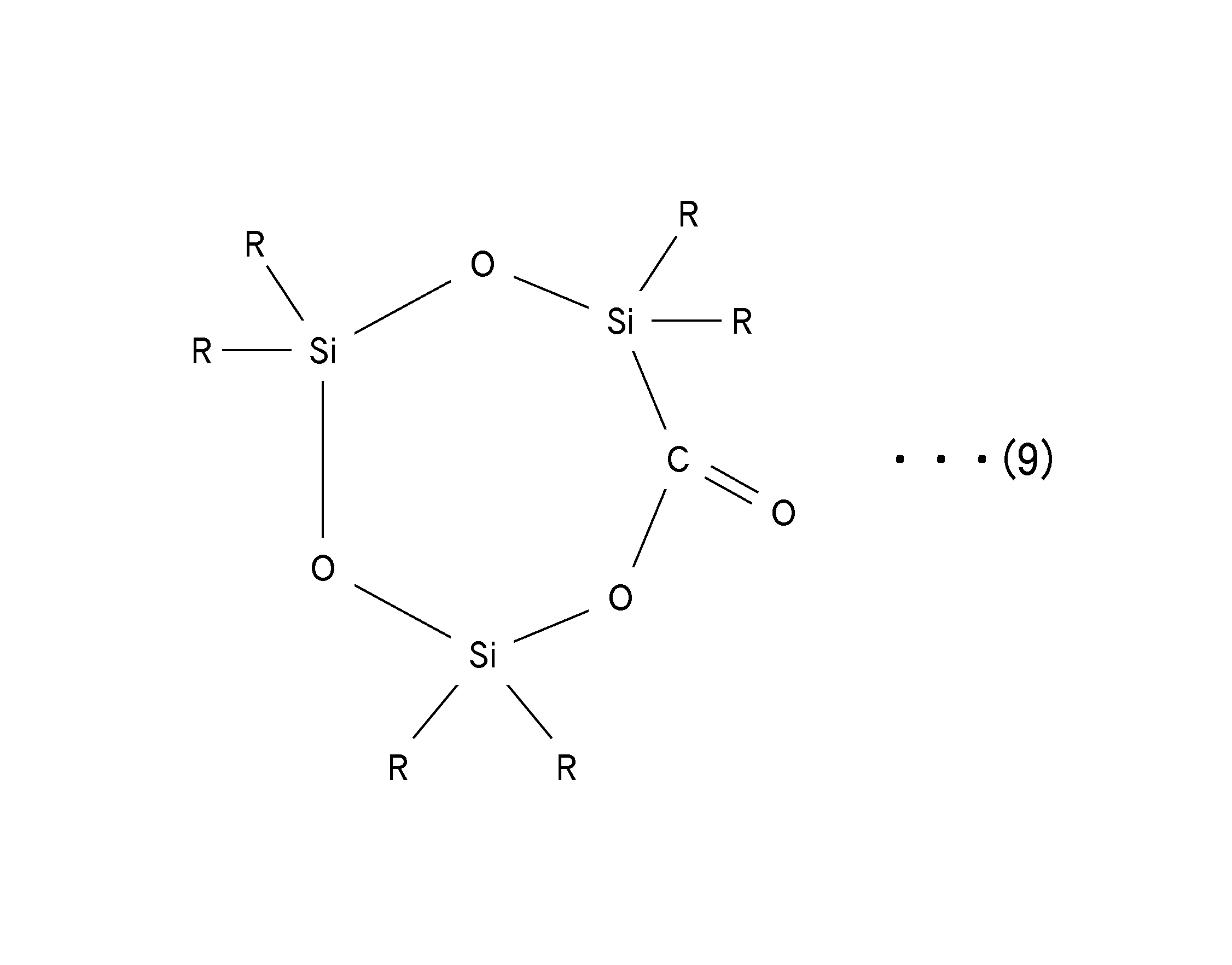
- a structure in which a carbonyl group enters a part of the skeleton of the cyclic siloxane a structure in which a part of Si of the cyclic siloxane is substituted with a carbonyl group as shown in the following structural formula (8) can also be used.
- the bond energy between the carbonyl group C and the cyclic siloxane O is 3.5 eV, which is smaller than the bond energy of the other bonds.
- O and O are combined to form a stable compound having no dangling bond in the chemical structure.
- a structure in which a carbonyl group enters between Si and O of the cyclic siloxane can also be used. Also in this case, since the bond energy between C of the carbonyl group and Si of the cyclic siloxane and the bond energy of C of the carbonyl group and O of the cyclic siloxane are low as described above, the CO of the carbonyl group is preferentially eliminated, Si and O after the elimination of CO are combined to form a stable compound having no dangling bonds in terms of chemical structure.
- a structure in which an alkyl group is bonded to Si constituting the cyclic siloxane via a carbonyl group may be employed.
- the bond energy between carbonyl group C and cyclic siloxane Si is as low as 3.0 eV as described above, and the bond energy between carbonyl group C and alkyl group C is also as low as 3.4 eV.
- the CO of the carbonyl group is desorbed preferentially, and Si and the alkyl group after the desorption of CO are combined to form a stable compound having no dangling bond in chemical structure.
- a structure in which a group having a carbonyl group is bonded to Si constituting the cyclic siloxane may be employed. Also in this case, CO of the carbonyl group is desorbed preferentially, and C after desorption is bonded to form a stable compound having no dangling bond in chemical structure.
- the compound constituting the film-forming raw material of the present invention can be produced by applying a predetermined operation to an appropriate siloxane compound and then reacting with CO.
- the compound represented by the structural formula (3) is obtained by reacting hexamethyltrisiloxane with Cl 2 to form dichlorohexamethyltrisiloxane, and then dechlorinating with Na.
- the desorbed CO covers the surface of the film and the surface reaction is blocked, and the generation that contributes to the film formation generated by the desorption of CO. Since the active part does not exist in the product and is stable, the product is difficult to adhere to the film formation surface. For this reason, even if there is a recess with a large aspect ratio on the film formation surface, the surface of the inner wall in the recess is blocked by CO, and the product is a stable compound with no active part. The object does not adhere to the wall of the recess but enters the recess and reacts with O 2 which is an oxidant to deposit a silicon oxide film. Therefore, a silicon oxide film can be formed with good step coverage.
- a film forming method for forming a silicon oxide film by CVD using the silicon oxide film forming material of the present invention will be described.
- a CVD film forming apparatus an RLSA microwave plasma CVD that generates plasma by introducing microwaves into a processing chamber using an RLSA (Radial Line Slot Antenna) which is a planar antenna having a plurality of slots.
- RLSA Random Line Slot Antenna
- An example in which a silicon oxide film is formed using a film forming apparatus will be described.
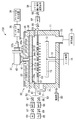
- FIG. 5 is a cross-sectional view showing such an RLSA microwave plasma CVD apparatus.
- the microwave plasma CVD film forming apparatus 100 has a substantially cylindrical grounded chamber (processing vessel) 11 made of a metal material such as aluminum or stainless steel, which is hermetically configured, and a substrate to be processed therein.
- a silicon oxide film is formed on a semiconductor wafer (hereinafter simply referred to as a wafer) W.
- a microwave introduction unit 30 for introducing a microwave into the processing space is provided on the upper portion of the chamber 11.
- a susceptor 12 for horizontally supporting a wafer W as a processing object is provided in a state of being supported by a cylindrical support member 13 erected at the center of the bottom of the chamber 11.
- a heater 15 for temperature adjustment is embedded in the susceptor 12.
- a heater power supply 16 is connected to the heater 15, and the heater 15 is supplied with power from the power supply 16 to generate heat, and the wafer W is heated to a predetermined temperature via the susceptor 12.
- the susceptor 12 is provided with three wafer support pins (not shown) for supporting the wafer W and moving it up and down so as to protrude and retract with respect to the surface of the susceptor 12.
- An exhaust pipe 25 is connected to the bottom of the chamber 11, and an exhaust device 26 including an automatic pressure control valve and a high-speed vacuum pump is connected to the exhaust pipe 25. Then, by operating this exhaust device 26, the inside of the chamber 11 is exhausted, and the inside of the chamber 11 can be depressurized at a high speed to a predetermined degree of vacuum. Further, on the side wall of the chamber 11, a loading / unloading port 70 for loading / unloading the wafer W and a gate valve 71 for opening / closing the loading / unloading port 70 are provided.
- the microwave introduction unit 30 includes a microwave transmission plate 28, a planar antenna 31, and a slow wave material 33 in order from the susceptor 12 side. These are covered by a shield member 34, a presser ring 36 and an upper plate 29, and are fixed by an annular presser ring 35. In the state where the microwave introduction part 30 is closed, the upper end of the chamber 11 and the upper plate 29 are sealed by a seal member (not shown) and, as will be described later, through the microwave transmission plate 28. Thus, the upper plate 29 is supported.
- the microwave transmission plate 28 is made of a dielectric material such as quartz, Al 2 O 3 , AlN, sapphire, or SiN, and functions as a microwave introduction window that transmits microwaves and introduces them into the processing space in the chamber 11. .
- the lower surface (susceptor 12 side) of the microwave transmission plate 28 is not limited to a flat shape, and for example, a recess or a groove may be formed in order to make the microwave uniform and stabilize the plasma.
- the microwave transmission plate 28 is supported in an airtight state via a seal member (not shown) by a protrusion 29a on the inner peripheral surface of an upper plate 29 disposed annularly below the outer periphery of the microwave introduction portion 30. ing. Therefore, the inside of the chamber 11 can be kept airtight.
- the planar antenna 31 has a disk shape and is locked to the inner peripheral surface of the shield member 34 at a position above the microwave transmitting plate 28.
- the planar antenna 31 is made of, for example, a copper plate or an aluminum plate plated with gold or silver, and a plurality of slot holes 31a for radiating electromagnetic waves such as microwaves are formed in a predetermined pattern so that the RLSA is formed. It is composed.
- the slow wave material 33 has a dielectric constant larger than that of the vacuum, and is provided on the upper surface of the planar antenna 31.
- This slow wave material 33 is made of a dielectric material such as a fluororesin such as quartz, ceramics, polytetrafluoroethylene, or a polyimide resin, and the wavelength of the microwave becomes longer in vacuum. It has the function of adjusting the plasma by shortening the wavelength of the microwave.
- the planar antenna 31 and the microwave transmitting plate 28, and the slow wave member 33 and the planar antenna 31 may be in close contact with each other or separated from each other.
- a cooling water flow path 34a is formed in the shield member 34, and the shield member 34, the slow wave material 33, the planar antenna 31, and the microwave transmission plate 28 are cooled by allowing the cooling water to flow therethrough. It has become.
- the shield member 34 is grounded.
- An opening 34b is formed at the center of the shield member 34, and a waveguide 37 is connected to the opening 34b.
- a microwave generator 39 is connected to the end of the waveguide 37 via a matching circuit 38. Thereby, for example, a microwave having a frequency of 2.45 GHz generated by the microwave generator 39 is propagated to the planar antenna 31 through the waveguide 37.
- the microwave frequency 8.35 GHz, 1.98 GHz, or the like can be used.
- the waveguide 37 is connected to a coaxial waveguide 37 a having a circular cross section extending upward from the opening 34 b of the shield member 34, and an upper end portion of the coaxial waveguide 37 a via a mode converter 40. And a rectangular waveguide 37b extending in the horizontal direction.
- the mode converter 40 between the rectangular waveguide 37b and the coaxial waveguide 37a has a function of converting the microwave propagating in the TE mode in the rectangular waveguide 37b into the TEM mode.
- An inner conductor 41 extends in the center of the coaxial waveguide 37a, and the inner conductor 41 is connected and fixed to the center of the planar antenna member 31 at its lower end. As a result, the microwave is efficiently and uniformly propagated radially and uniformly to the planar antenna member 31 via the inner conductor 41 of the coaxial waveguide 37a.
- a shower plate 51 for introducing a film forming raw material gas for a silicon oxide film is provided horizontally.
- the shower plate 51 includes a gas flow path 52 formed in a lattice shape and a large number of gas discharge holes 53 formed in the gas flow path 52.
- a space 54 is formed.
- a pipe 55 extending outside the chamber 11 is connected to the gas flow path 52 of the shower plate 51.
- a film forming material gas supply source 56 for silicon oxide film is connected to the pipe 55.
- the pipe 55 is provided with a mass flow controller 57 for flow rate control and a pair of valves 58 provided before and after the mass flow controller 57.
- a siloxane compound having a carbonyl group as described above is used as a film forming source gas for a silicon oxide film.
- the film forming raw material for the silicon oxide film is liquid at normal temperature, it is supplied after being vaporized by an appropriate method such as bubbling, heating, vaporization by a vaporizer or the like.
- a ring-shaped plasma gas introduction member 60 is provided along the chamber wall above the shower plate 51 of the chamber 11, and the plasma gas introduction member 60 has a number of gas discharge holes on the inner periphery. Is provided.
- a pipe 61 is connected to the plasma gas introduction member 60, and the pipe 61 branches into an Ar gas pipe 62 and an O 2 gas pipe 63, and is connected to an Ar gas supply source 64 and an O 2 gas supply source 65, respectively. It is connected.
- the Ar gas pipe 62 is provided with a mass flow controller 66 for flow rate control and a pair of valves 67 provided before and after the mass flow controller 66.
- the O 2 gas pipe 63 is provided with a mass flow controller 68 for flow rate control and a pair of valves 69 provided before and after the mass flow controller 68.
- Ar gas introduced into the chamber 11 from the Ar gas supply source 64 is turned into plasma by the microwave introduced into the chamber 11 via the microwave introduction unit 30, and this plasma is converted from the O 2 gas supply source 65 to the chamber. 11, the O 2 gas introduced into the plasma 11 is turned into plasma, and the plasma acts on the film forming material gas for the silicon oxide film that passes through the space 54 of the shower plate 51 and is discharged from the gas discharge hole 53 of the shower plate 51. .
- the control unit 80 is configured by a computer, a controller (microprocessor) that performs arithmetic processing, a keyboard that allows an operator to input commands to manage each component of the microwave plasma CVD apparatus 100, and the operation of the apparatus 100
- a user interface comprising a display for visualizing and displaying the situation, and a control program for realizing various processes executed by the microwave plasma CVD film forming apparatus 100 under the control of the controller, and etching according to processing conditions
- a storage unit storing a program for causing each component unit of the apparatus 100 to execute processing, that is, a processing recipe, is connected.
- the processing recipe is stored in a state stored in a storage medium.
- the storage medium may be a fixed one such as a hard disk or a portable one such as a semiconductor memory, a CDROM, or a DVD. Furthermore, you may make it transmit a recipe suitably from another apparatus via a dedicated line, for example. Then, if necessary, an arbitrary recipe is called by an instruction from the user interface or the like, and is executed by the controller, so that processing in the microwave plasma CVD film forming apparatus 100 is performed.
- the susceptor 12 is heated to a predetermined temperature by the heater 15, and the wafer W is loaded into the chamber 11 and placed on the susceptor 12.
- the wafer W is heated to 100 to 400 ° C., for example, and then evacuated so that the pressure in the chamber 11 becomes 1.33 to 1330 Pa (10 mTorr to 10 Torr).
- the microwave from the microwave generator 39 is guided to the waveguide 37 through the matching circuit 38, the rectangular waveguide 37b, the mode converter 40, and the coaxial waveguide 37a.
- the microwave propagates in the rectangular waveguide 37b in the TE mode, and the TE mode microwave is converted into the TEM mode by the mode converter 40, and the coaxial waveguide 37a is directed toward the planar antenna member 31.
- the microwave is radiated from the planar antenna member 31 to the chamber 11 through the transmission plate 28, and an electromagnetic field is formed in the chamber 11 by the microwave, and the Ar gas that is a plasma generation gas is turned into plasma. .
- the O 2 gas from the O 2 gas supply source 65 is introduced into the chamber 11 into a plasma by Ar plasma from the gas discharge holes 53 of the shower plate 51 the plasma passes through the space 54 of the shower plate 51 It acts on the discharged film forming source gas for silicon oxide film.
- the film forming raw material for the silicon oxide film is made of a siloxane compound having a carbonyl group, decomposed by application of energy, desorbed CO, and formed into a film formed by desorbing CO. Since the product that contributes to the chemical structure is such that no dangling bond exists, CO is desorbed by the plasma energy, and the product that contributes to film formation after the desorption has a dangling bond due to the chemical structure. It will not do.
- the plasma formed during the film formation has a high density of about 1 ⁇ 10 10 to 5 ⁇ 10 12 / cm 3 by radiating microwaves from a number of slot holes 32 of the planar antenna 31, and In the vicinity of the wafer W, low electron temperature plasma of about 1.5 eV or less is obtained. Therefore, a good quality silicon oxide film can be formed without damaging the base.
- the present invention is not limited to the above embodiment and can be variously modified.
- the RLSA microwave plasma CVD film forming apparatus is used as the silicon oxide film forming apparatus.
- the present invention is not limited to this, and an inductively coupled plasma CVD film forming apparatus or a capacitively coupled type (parallel plate type) is used.
- Other plasma CVD film forming apparatuses such as a plasma CVD film forming apparatus may be used, and not only the plasma CVD film forming apparatus but also a thermal CVD film forming apparatus that uses only thermal energy without using plasma energy may be used.
- the oxidizing agent is not limited to O 2 gas, but may be other gas such as H 2 O, O 3 .
- Ar gas is used as the plasma generating gas, other gas such as He may be used, or only the film forming raw material gas and the oxidizing agent may be used without using the plasma generating gas.
- the substrate to be processed is not limited to a semiconductor wafer, and may be another substrate such as an FPD substrate typified by a substrate for a liquid crystal display device.
Landscapes
- Chemical & Material Sciences (AREA)
- Chemical Kinetics & Catalysis (AREA)
- General Chemical & Material Sciences (AREA)
- Engineering & Computer Science (AREA)
- Materials Engineering (AREA)
- Mechanical Engineering (AREA)
- Metallurgy (AREA)
- Organic Chemistry (AREA)
- Inorganic Chemistry (AREA)
- Chemical Vapour Deposition (AREA)
- Formation Of Insulating Films (AREA)
Abstract
Description
(1)アスペクト比が大きい凹部に高ステップカバレッジでシリコン酸化膜を形成するためには、付着係数の小さい、すなわち付着しにくい成膜原料を用いる必要があること。
(2)成膜原料として、カルボニル基を有するシロキサン系化合物からなり、成膜処理の際にCOが脱離し、さらにCOの脱離によって生成した生成物が、化学構造上ダングリングボンドが存在しないものとなるような化合物を用いれば、脱離したCOが成膜表面を覆って表面反応がブロックされるとともに、生成物に活性な部分が存在せず安定であるため、生成物が成膜表面に付着し難くなること。
本発明に係るシリコン酸化膜用成膜原料は、化学蒸着(CVD)法により基板上にシリコン酸化膜を成膜するためのものである。





ここでは、CVD成膜装置として、複数のスロットを有する平面アンテナであるRLSA(Radial Line Slot Antenna;ラジアルラインスロットアンテナ)にて処理室内にマイクロ波を導入してプラズマを発生させるRLSAマイクロ波プラズマCVD成膜装置を用いてシリコン酸化膜を形成する例について説明する。
Claims (11)
- 化学蒸着法により基板上にシリコン酸化膜を成膜するためのシリコン酸化膜用成膜原料であって、カルボニル基を有するシロキサン系化合物からなり、エネルギーが与えられることにより分解してCOが脱離し、化学構造上ダングリングボンドが存在しない生成物が生成され、その生成物が成膜に寄与する、シリコン酸化膜用成膜原料。
- 環状シロキサンの骨格の一部にカルボニル基が入り込んだ構造を有する、請求項1に記載のシリコン酸化膜用成膜原料。
- 環状シロキサンを構成するSiの一部をカルボニル基で置換した構造を有する、請求項2に記載のシリコン酸化膜用成膜原料。
- 環状シロキサンを構成するOの一部をカルボニル基で置換した構造を有する、請求項2に記載のシリコン酸化膜用成膜原料。
- 環状シロキサンを構成するSiとOとの間の一部にカルボニル基が入り込んだ構造を有する、請求項2に記載のシリコン酸化膜用成膜原料。
- 環状シロキサンを構成するSiにカルボニル基を介してアルキル基が結合した構造を有する、請求項2に記載のシリコン酸化膜用成膜原料。
- 環状シロキサンを構成するSiにカルボニル基を有する基が結合した構造を有する、請求項2に記載のシリコン酸化膜用成膜原料。
- 処理容器内に被処理基板を配置することと、
前記処理容器内に、カルボニル基を有するシロキサン系化合物からなり、エネルギーが与えられることにより分解してCOが脱離し、化学構造上ダングリングボンドが存在しない生成物が生成され、その生成物が成膜に寄与する、シリコン酸化膜用成膜原料と、酸化剤とを導入することと、
前記シリコン酸化膜用成膜原料にエネルギーを与えてCOを脱離させ、それにより生成された化学構造上ダングリングボンドが存在しない生成物を成膜表面に付着させ、その生成物と酸化剤との反応により被処理基板上にシリコン酸化膜を成膜する、シリコン酸化膜の成膜方法。 - 前記エネルギーは前記処理容器内にプラズマを生成することにより与えられる、請求項8に記載のシリコン酸化膜の成膜方法。
- 前記プラズマはマイクロ波により生成される、請求項9に記載のシリコン酸化膜の成膜方法。
- 前記プラズマは平面アンテナから放射されたマイクロ波によって形成される、請求項10に記載のシリコン酸化膜の成膜方法。
Priority Applications (3)
| Application Number | Priority Date | Filing Date | Title |
|---|---|---|---|
| US13/375,346 US8753988B2 (en) | 2009-06-03 | 2010-05-27 | Starting material for use in forming silicon oxide film and method for forming silicon oxide film using same |
| KR1020117024723A KR101321155B1 (ko) | 2009-06-03 | 2010-05-27 | 실리콘 산화막용 성막 원료 및 그것을 이용한 실리콘 산화막의 성막 방법 |
| CN2010800245009A CN102804348A (zh) | 2009-06-03 | 2010-05-27 | 硅氧化膜用成膜原料及使用该原料的硅氧化膜的成膜方法 |
Applications Claiming Priority (2)
| Application Number | Priority Date | Filing Date | Title |
|---|---|---|---|
| JP2009134278A JP5559988B2 (ja) | 2009-06-03 | 2009-06-03 | シリコン酸化膜用成膜原料およびそれを用いたシリコン酸化膜の成膜方法 |
| JP2009-134278 | 2009-06-03 |
Publications (1)
| Publication Number | Publication Date |
|---|---|
| WO2010140529A1 true WO2010140529A1 (ja) | 2010-12-09 |
Family
ID=43297665
Family Applications (1)
| Application Number | Title | Priority Date | Filing Date |
|---|---|---|---|
| PCT/JP2010/058984 Ceased WO2010140529A1 (ja) | 2009-06-03 | 2010-05-27 | シリコン酸化膜用成膜原料およびそれを用いたシリコン酸化膜の成膜方法 |
Country Status (6)
| Country | Link |
|---|---|
| US (1) | US8753988B2 (ja) |
| JP (1) | JP5559988B2 (ja) |
| KR (1) | KR101321155B1 (ja) |
| CN (1) | CN102804348A (ja) |
| TW (1) | TW201109341A (ja) |
| WO (1) | WO2010140529A1 (ja) |
Families Citing this family (5)
| Publication number | Priority date | Publication date | Assignee | Title |
|---|---|---|---|---|
| KR102106885B1 (ko) | 2013-03-15 | 2020-05-06 | 삼성전자 주식회사 | 실리콘 산화막 증착용 전구체 조성물 및 상기 전구체 조성물을 이용한 반도체 소자 제조 방법 |
| SG11201703196WA (en) | 2014-10-24 | 2017-05-30 | Versum Materials Us Llc | Compositions and methods using same for deposition of silicon-containing films |
| US10468264B2 (en) * | 2016-07-04 | 2019-11-05 | Samsung Electronics Co., Ltd. | Method of fabricating semiconductor device |
| CN114497199B (zh) * | 2020-10-23 | 2024-05-17 | 长鑫存储技术有限公司 | 半导体结构及其制作方法 |
| US12112973B2 (en) | 2020-10-23 | 2024-10-08 | Changxin Memory Technologies, Inc. | Semiconductor structure and method for manufacturing the same |
Citations (3)
| Publication number | Priority date | Publication date | Assignee | Title |
|---|---|---|---|---|
| JPH10279643A (ja) * | 1997-04-07 | 1998-10-20 | Dow Corning Corp | 重合方法 |
| JP2005252012A (ja) * | 2004-03-04 | 2005-09-15 | Advanced Lcd Technologies Development Center Co Ltd | 成膜方法、半導体素子の形成方法、半導体装置、及び表示装置 |
| JP2007318067A (ja) * | 2006-04-27 | 2007-12-06 | National Institute For Materials Science | 絶縁膜材料、この絶縁膜材料を用いた成膜方法および絶縁膜 |
Family Cites Families (6)
| Publication number | Priority date | Publication date | Assignee | Title |
|---|---|---|---|---|
| US2989559A (en) * | 1958-06-27 | 1961-06-20 | Union Carbide Corp | Carbonyl-containing organopolysiloxanes |
| JPH09162184A (ja) * | 1995-12-07 | 1997-06-20 | Sony Corp | 半導体装置の製造方法 |
| US7345000B2 (en) * | 2003-10-10 | 2008-03-18 | Tokyo Electron Limited | Method and system for treating a dielectric film |
| JP4624207B2 (ja) | 2005-08-03 | 2011-02-02 | 東京エレクトロン株式会社 | 成膜方法及び成膜装置 |
| TW200710260A (en) | 2005-08-10 | 2007-03-16 | Taiyo Nippon Sanso Corp | Material for an insulating film, film forming method and insulating film using the same |
| JP4451457B2 (ja) * | 2007-02-26 | 2010-04-14 | 富士通株式会社 | 絶縁膜材料及びその製造方法、多層配線及びその製造方法、並びに、半導体装置の製造方法 |
-
2009
- 2009-06-03 JP JP2009134278A patent/JP5559988B2/ja not_active Expired - Fee Related
-
2010
- 2010-05-27 CN CN2010800245009A patent/CN102804348A/zh active Pending
- 2010-05-27 WO PCT/JP2010/058984 patent/WO2010140529A1/ja not_active Ceased
- 2010-05-27 KR KR1020117024723A patent/KR101321155B1/ko not_active Expired - Fee Related
- 2010-05-27 US US13/375,346 patent/US8753988B2/en not_active Expired - Fee Related
- 2010-06-02 TW TW099117776A patent/TW201109341A/zh unknown
Patent Citations (3)
| Publication number | Priority date | Publication date | Assignee | Title |
|---|---|---|---|---|
| JPH10279643A (ja) * | 1997-04-07 | 1998-10-20 | Dow Corning Corp | 重合方法 |
| JP2005252012A (ja) * | 2004-03-04 | 2005-09-15 | Advanced Lcd Technologies Development Center Co Ltd | 成膜方法、半導体素子の形成方法、半導体装置、及び表示装置 |
| JP2007318067A (ja) * | 2006-04-27 | 2007-12-06 | National Institute For Materials Science | 絶縁膜材料、この絶縁膜材料を用いた成膜方法および絶縁膜 |
Also Published As
| Publication number | Publication date |
|---|---|
| US8753988B2 (en) | 2014-06-17 |
| JP2010283077A (ja) | 2010-12-16 |
| US20120071006A1 (en) | 2012-03-22 |
| KR101321155B1 (ko) | 2013-10-22 |
| KR20120011014A (ko) | 2012-02-06 |
| TW201109341A (en) | 2011-03-16 |
| CN102804348A (zh) | 2012-11-28 |
| JP5559988B2 (ja) | 2014-07-23 |
Similar Documents
| Publication | Publication Date | Title |
|---|---|---|
| JP6742165B2 (ja) | 窒化珪素膜の処理方法および窒化珪素膜の形成方法 | |
| KR101364834B1 (ko) | 플라즈마 질화 처리 방법 | |
| KR20200143254A (ko) | 개질 가스를 사용하여 전자 구조를 형성하는 방법, 상기 방법을 수행하기 위한 시스템, 및 상기 방법을 사용하여 형성되는 구조 | |
| JP2011199003A (ja) | シリコン酸化膜の形成方法、及びプラズマ処理装置 | |
| JP2011077321A (ja) | 選択的プラズマ窒化処理方法及びプラズマ窒化処理装置 | |
| WO2012011480A1 (ja) | 層間絶縁層形成方法及び半導体装置 | |
| JP2009170788A (ja) | アモルファスカーボン膜の処理方法およびそれを用いた半導体装置の製造方法 | |
| JP2007042951A (ja) | プラズマ処理装置 | |
| JP6832785B2 (ja) | シリコン窒化膜の成膜方法および成膜装置 | |
| JP5559988B2 (ja) | シリコン酸化膜用成膜原料およびそれを用いたシリコン酸化膜の成膜方法 | |
| US10151029B2 (en) | Silicon nitride film forming method and silicon nitride film forming apparatus | |
| JP5078617B2 (ja) | 選択的プラズマ処理方法およびプラズマ処理装置 | |
| JP4509864B2 (ja) | プラズマ処理方法およびプラズマ処理装置 | |
| JP2011077228A (ja) | プラズマ処理装置及びこれに用いる遅波板 | |
| EP1742273A1 (en) | Method of forming gate insulating film, storage medium and computer program | |
| WO2010038885A1 (ja) | 窒化珪素膜およびその形成方法、コンピュータ読み取り可能な記憶媒体並びにプラズマcvd装置 | |
| JP2010087185A (ja) | シリコン酸化膜の形成方法、コンピュータ読み取り可能な記憶媒体およびプラズマ酸化処理装置 | |
| JP2008251959A (ja) | 絶縁層の形成方法及び半導体装置の製造方法 | |
| WO2025033230A1 (ja) | 成膜方法および成膜システム | |
| JPWO2010038888A1 (ja) | 窒化酸化珪素膜およびその形成方法、コンピュータ読み取り可能な記憶媒体並びにプラズマcvd装置 |
Legal Events
| Date | Code | Title | Description |
|---|---|---|---|
| WWE | Wipo information: entry into national phase |
Ref document number: 201080024500.9 Country of ref document: CN |
|
| 121 | Ep: the epo has been informed by wipo that ep was designated in this application |
Ref document number: 10783313 Country of ref document: EP Kind code of ref document: A1 |
|
| ENP | Entry into the national phase |
Ref document number: 20117024723 Country of ref document: KR Kind code of ref document: A |
|
| WWE | Wipo information: entry into national phase |
Ref document number: 13375346 Country of ref document: US |
|
| NENP | Non-entry into the national phase |
Ref country code: DE |
|
| 122 | Ep: pct application non-entry in european phase |
Ref document number: 10783313 Country of ref document: EP Kind code of ref document: A1 |