WO2010140510A1 - サンドブラスト処理を施した貼り合わせ基板の結晶品質改善方法 - Google Patents
サンドブラスト処理を施した貼り合わせ基板の結晶品質改善方法 Download PDFInfo
- Publication number
- WO2010140510A1 WO2010140510A1 PCT/JP2010/058827 JP2010058827W WO2010140510A1 WO 2010140510 A1 WO2010140510 A1 WO 2010140510A1 JP 2010058827 W JP2010058827 W JP 2010058827W WO 2010140510 A1 WO2010140510 A1 WO 2010140510A1
- Authority
- WO
- WIPO (PCT)
- Prior art keywords
- cleaning
- substrate
- layer
- etching
- peeling
- Prior art date
- Legal status (The legal status is an assumption and is not a legal conclusion. Google has not performed a legal analysis and makes no representation as to the accuracy of the status listed.)
- Ceased
Links
Images



Classifications
-
- B—PERFORMING OPERATIONS; TRANSPORTING
- B24—GRINDING; POLISHING
- B24C—ABRASIVE OR RELATED BLASTING WITH PARTICULATE MATERIAL
- B24C1/00—Methods for use of abrasive blasting for producing particular effects; Use of auxiliary equipment in connection with such methods
- B24C1/06—Methods for use of abrasive blasting for producing particular effects; Use of auxiliary equipment in connection with such methods for producing matt surfaces, e.g. on plastic materials, on glass
-
- H—ELECTRICITY
- H10—SEMICONDUCTOR DEVICES; ELECTRIC SOLID-STATE DEVICES NOT OTHERWISE PROVIDED FOR
- H10P—GENERIC PROCESSES OR APPARATUS FOR THE MANUFACTURE OR TREATMENT OF DEVICES COVERED BY CLASS H10
- H10P10/00—Bonding of wafers, substrates or parts of devices
- H10P10/12—Bonding of semiconductor wafers or semiconductor substrates to semiconductor wafers or semiconductor substrates
- H10P10/128—Bonding of semiconductor wafers or semiconductor substrates to semiconductor wafers or semiconductor substrates by direct semiconductor to semiconductor bonding
-
- H—ELECTRICITY
- H10—SEMICONDUCTOR DEVICES; ELECTRIC SOLID-STATE DEVICES NOT OTHERWISE PROVIDED FOR
- H10P—GENERIC PROCESSES OR APPARATUS FOR THE MANUFACTURE OR TREATMENT OF DEVICES COVERED BY CLASS H10
- H10P50/00—Etching of wafers, substrates or parts of devices
- H10P50/60—Wet etching
- H10P50/64—Wet etching of semiconductor materials
- H10P50/642—Chemical etching
- H10P50/644—Anisotropic liquid etching
-
- H—ELECTRICITY
- H10—SEMICONDUCTOR DEVICES; ELECTRIC SOLID-STATE DEVICES NOT OTHERWISE PROVIDED FOR
- H10P—GENERIC PROCESSES OR APPARATUS FOR THE MANUFACTURE OR TREATMENT OF DEVICES COVERED BY CLASS H10
- H10P70/00—Cleaning of wafers, substrates or parts of devices
- H10P70/10—Cleaning before device manufacture, i.e. Begin-Of-Line process
- H10P70/15—Cleaning before device manufacture, i.e. Begin-Of-Line process by wet cleaning only
Definitions
- the present invention relates to a method for improving the crystal quality of a bonded substrate such as a SOQ, SOG, or SOS substrate subjected to sandblasting.
- Sandblasting may be used when fogging (frosting) a glass / quartz or other SiO 2 -based substrate / component or a sapphire-based substrate / component.
- This is a method in which fine powder of alumina or silica is sprayed on the surface to be roughened and is widely used for various purposes.
- Silicon on Quartz (SOQ), Silicon on Glass (SOG), and Silicon on Sapphire (SOS) substrates with single-crystal silicon thin films are put into the same CMOS process as ordinary silicon wafers. It is particularly important to intentionally roughen the back surface from the meaning of preventing slipping of the conveyance or the conveyance sensor.
- the procedure for sandblasting when manufacturing the SOQ, SOG, and SOS substrates will be described below.
- the simplest method is a protective tape (for back grind, Dicing) is applied to the silicon side.
- the sandblasting surface is cleaned with hydrogen fluoride (HF), etc., if necessary, then the tape is peeled off, and the silicon surface is polished and cleaned. Can be considered.
- HF hydrogen fluoride
- SiGen method plasma treatment is applied to one or both of the donor substrate and the handle substrate that have been ion-implanted, and then peeled off mechanically
- SOITEC method SOITEC method
- a damaged layer of about 0.15 ⁇ m remains in the silicon layer immediately after delamination. Therefore, it is necessary to remove this layer (see, for example, Non-Patent Document 1). Removing all the damaged layers by polishing increases the film thickness variation, so in the actual process, most of them are removed by chemical etching, and then the surface is mirrored by polishing. Is reasonable.
- the process in this case is as follows.
- a tape typified by a UV curable tape (a tape whose adhesive strength is reduced by being irradiated with UV light and which can be easily detached) is used.
- an alkaline etching solution is used for etching after the protective tape is peeled off.
- the object of the present invention is to provide a sandblasting process on the handle substrate side after protecting the surface of the bonding layer in advance after forming the bonding layer on the handle substrate by ion implantation / peeling method in view of the above situation.
- an object of the present invention is to provide a method for preventing the occurrence of minute defects in the step of removing the peeling damage layer of the Si layer by etching to form a donor thin film.
- the present invention has been made to solve the above problems. That is, a method for manufacturing a bonded substrate provided with a donor thin film on a handle substrate, the step of forming a bonded layer on the handle substrate by an ion implantation / peeling method, and a surface of the bonded layer with a protective member Coating the surface of the handle substrate, subjecting the surface of the handle substrate to a sandblast treatment, peeling the protective member, and cleaning the surface of the bonded layer after removing the protective member without etching action.
- a method for manufacturing a bonded substrate including a step and a step of chemically etching a surface of a bonding layer after the cleaning step to form the donor thin film.
- the void defect can be greatly reduced by entering the etching process after removing or modifying the residual organic matter by the method for manufacturing a bonded substrate according to the present invention.
- FIG. 5 shows a method for manufacturing a bonded substrate including a donor thin film on a handle substrate.
- the bonding layer 102 is formed on the handle substrate 103 by ion implantation / peeling.
- a peeling damage layer of about 0.15 ⁇ m is formed on the surface of the bonding layer 102.
- the surface of the bonding layer 102 is covered with a protective member 105.
- the handle substrate surface 107 is subjected to sandblasting, and the protective member 105 is peeled off. Thereafter, in order to remove the peeling damage layer, the surface of the bonding layer is chemically etched to form the donor thin film 109.
- minute defects 108 are formed on the surface of the donor thin film 109.
- the bonding layer 102 is combined with the etching solution and the organic residue in the next etching step. As a result, it was found that these fine defects 108 were generated by selective and early etching.
- the alkaline solution has the ability to remove the organic residue 106, it has been found to leave voids in the silicon layer before it is completely removed.
- FIG. 1 shows a series of steps of a method for manufacturing a bonded substrate of the present invention developed based on the above examination results.
- the method for producing a bonded substrate of the present invention can be suitably applied to a substrate immediately after forming a bonded layer on a handle substrate, particularly an SOQ, SOG, and SOS substrate after thin film transfer.
- the handle substrate is preferably made of quartz, glass, or sapphire
- the bonding layer is preferably a silicon layer.
- Examples of the method for forming the bonding layer on the handle substrate include an ion implantation / peeling method.
- an ion implantation layer is formed by implanting hydrogen ions and / or rare gas ions from the surface of a donor substrate or a donor substrate having an oxide film formed on the surface.
- An ion-implanted surface of a donor substrate having an oxide film formed thereon and one surface of a handle substrate are bonded together after being subjected to surface activation treatment, and the donor substrate is bounded by using the ion-implanted layer as a boundary.
- the silicon substrate with an oxide film formed on the surface is peeled off to reduce the thickness.
- the bonding layer by the ion implantation / peeling method it may be possible to use a handle substrate whose surface is roughened in advance, but it is transferred because the stress at the time of peeling is locally different. This is not desirable because the thickness of the donor thin film varies.
- the stress at the time of peeling is locally different because the adhesion force with the stiffener plate is locally different. This is because there is a possibility that the film thickness of the silicon transferred to the film may vary.
- the protective member is preferably a backgrinding protective tape, a dicing tape, or a die bonding tape.
- the sandblasting process (S3) is performed on the handle substrate surface.
- Roughening by sandblasting makes it easy to remove after transporting and mounting.
- the sandblast surface is cleaned with a solution containing HF or the like as required (S4). This is because if the powder remains, the surface of the bonding layer may be contaminated.
- S4 a solution containing HF or the like as required
- the protective member is peeled off (S5).
- S5 Although it does not specifically limit as a method of peeling a protective member, When using a UV hardening tape, UV hardening process is mentioned.
- a step (S6) of performing cleaning without etching action on the surface of the bonded layer is included.
- the cleaning method preferably includes at least one of UV dry cleaning, UV ozone cleaning, sulfuric acid cleaning, and sulfuric acid / hydrogen peroxide, and two or more cleaning methods (SPM) cleaning or plasma cleaning (ashing) is used. It is also possible to use it.
- the atmosphere is 1 type, or 2 or more types of mixed gas selected from the group which consists of oxygen, argon, and nitrogen.
- etching solution used for the chemical etching is preferably one or a combination of two or more selected from the group consisting of ammonia overwater, ammonia, KOH, NaOH, CsOH, TMAH, EDP, and hydrazine.
- the final film thickness of the donor thin film is not particularly limited, but can be 50 nm to 500 nm.
- an organic solvent has a slower etching rate than an alkaline solution, and is therefore suitable when precise etching amount control is required.
- a bonded substrate of different materials in which a donor thin film such as silicon is formed on the surface of an insulating substrate such as quartz, glass, sapphire, etc., as well as TFT-LCD and high frequency (RF ) Suitable for devices, other MEMS products, etc.
- a donor thin film such as silicon is formed on the surface of an insulating substrate such as quartz, glass, sapphire, etc.
- RF high frequency
- a 150 mm quartz substrate manufactured by Shin-Etsu Chemical Co., Ltd., thickness: 625 ⁇ m
- a single crystal silicon substrate (manufactured by Shin-Etsu Chemical Co., Ltd.) was prepared by growing an oxide film having a diameter of 150 mm and a thickness of 200 nm.
- Hydrogen ions were implanted into the bonding surface of the silicon substrate to the handle substrate to form an ion implantation layer.
- the ion implantation conditions were such that the implantation energy was 55 keV.
- a plurality of SOQ substrates (diameter 150 mm, thickness 625 um, silicon layer thickness 400 nm) immediately after peeling are prepared, each is coated with a dicing tape (product number: D636, manufactured by Lintec), and the surface on the quartz substrate side is sandblasted. Was given. Thereafter, the wafer was immersed in 2% hydrofluoric acid for cleaning, dried, UV cured, and the tape was peeled off. Subsequently, the following processing was performed on separate wafers.
- the 120 nm silicon layer was removed by etching, followed by 50 nm polishing (CMP polishing).
- the alkaline solution used for etching is SC1 solution, and the amount of hydrogen peroxide water is intentionally reduced to enhance the etching effect.
- the wafer is immersed in a 10% HF solution for 10 minutes for inspection, and the underlying quartz layer is etched through the void defect to make the defect easy to see, and then the number of defects of 0.2 ⁇ m or more is counted using a defect inspection apparatus. It was. The results are shown in FIG. From this figure, it was found that the measures (2) to (7) were effective, although there were some differences.
- Example 2 The same experiment as in Example 1 was performed. Only the etching solution was changed, and a 120 nm silicon layer was removed using a TMAH (Tetramethyl ammonium hydroxide) solution, followed by 50 nm polishing (CMP polishing). For inspection, the wafer was immersed in a 10% HF solution for 10 minutes, and the underlying quartz layer was etched through void defects to make the defects easy to see, and the number of defects was counted using a defect inspection apparatus. The results are shown in FIG. Although the number of defects is slightly different from that in Example 1, it has been found that the tendency is the same as that in Example 1. From this result, it was suggested that the etching solution used was not affected.
- TMAH Tetramethyl ammonium hydroxide
Landscapes
- Engineering & Computer Science (AREA)
- Mechanical Engineering (AREA)
- Mechanical Treatment Of Semiconductor (AREA)
- Weting (AREA)
Abstract
ハンドル基板上にSiGen法等でSi層を形成した後で、前もって貼り合わせ層表面を保護したうえで、サンドブラスト処理をハンドル基板側に施す場合に、エッチングによってSi層の剥離ダメージ層を除去しドナー薄膜を形成する工程で、微小欠陥が生じるのを防ぐ方法を提供する。 ハンドル基板上にドナー薄膜を備えた貼り合わせ基板の製造方法であって、前記ハンドル基板上にイオン注入・剥離法によって貼り合わせ層を形成する工程(S1)と、前記貼り合わせ層の表面を保護部材で被覆する工程(S2)と、前記ハンドル基板表面にサンドブラスト処理を施す工程(S3)と、前記保護部材を剥離する工程(S5)と、前記保護部材を剥離した後の貼り合わせ層の表面に対してエッチング作用が無い洗浄を施す工程(S6)と、前記洗浄工程の後に貼り合わせ層表面を化学エッチングして前記ドナー薄膜を形成する工程(S7)とを含む貼り合わせ基板の製造方法である。
Description
本発明は、サンドブラスト処理を施したSOQ、SOG、SOS基板等の貼り合わせ基板の結晶品質改善方法に関する。
ガラス・石英等のSiO2ベースの基板・部品やサファイアベースの基板・部品等の曇り処理(フロスト処理)をする際に、サンドブラスト法が用いられることがある。これはアルミナやシリカの微粉を荒らしたい面に吹き付ける方法であり、様々な用途に広く用いられている。特に単結晶シリコン薄膜を積層したSilicon on Quartz(SOQ)やSilicon on Glass(SOG)、Silicon on Sapphire(SOS)基板などは通常のシリコンウェーハと同じようなCMOSプロセスに投入されるため、ロボット・自動搬送の滑り止め、または搬送センサー対応の意味からも裏面を故意に荒らすことは特に重要である。
SOQ、SOG,SOS基板を製造する際のサンドブラスト処理の手順について以下に説明する。
まずサンドブラスト法では微粉がシリコン側を傷つけないために、SOQ、SOG,SOS基板のシリコン側を保護する必要があり、最も簡単な方法は半導体工程に広く用いられている保護テープ(バックグラインド用、ダイシング用)をシリコン側に貼ることであり、サンドブラスト処理後に、必要に応じてフッ化水素(HF)などでサンドブラスト面の洗浄を行い、その後にテープを剥がし、シリコン面を研磨・洗浄するという方法が考えられる。
まずサンドブラスト法では微粉がシリコン側を傷つけないために、SOQ、SOG,SOS基板のシリコン側を保護する必要があり、最も簡単な方法は半導体工程に広く用いられている保護テープ(バックグラインド用、ダイシング用)をシリコン側に貼ることであり、サンドブラスト処理後に、必要に応じてフッ化水素(HF)などでサンドブラスト面の洗浄を行い、その後にテープを剥がし、シリコン面を研磨・洗浄するという方法が考えられる。
上記裏面のサンドブラスト処理に引き続いて、SiGen法と呼ばれる方法(イオン注入を施したドナー基板とハンドル基板の片方もしくは双方にプラズマ処理を施し貼り合わせたのち、機械的に剥離を行う)やSOITEC法(イオン注入を施したドナー基板とハンドル基板を貼り合わせたのち、熱で剥離を行う方法)に代表されるイオン注入・剥離法では、剥離直後のシリコン層には0.15μm程度のダメージ層が残存するので(例えば、非特許文献1を参照。)、この層を取り除く必要がある。
ダメージ層全てを研磨で取り除くことは膜厚バラツキを増大させることになるので、実際のプロセスでは、大部分を化学的なエッチング方法で除去し、然る後に研磨で表面を鏡面化するという方法が合理的である。
この場合のプロセスは以下の通りとなる。
ダメージ層全てを研磨で取り除くことは膜厚バラツキを増大させることになるので、実際のプロセスでは、大部分を化学的なエッチング方法で除去し、然る後に研磨で表面を鏡面化するという方法が合理的である。
この場合のプロセスは以下の通りとなる。
薄膜転写後のSOQ、SOG、SOS基板⇒Si層側に保護テープ貼り⇒サンドブラスト処理⇒(必要に応じて)サンドブラスト面の洗浄⇒テープ剥がし⇒剥離ダメージ層の化学エッチング⇒研磨・洗浄
ここで用いる保護テープはUV硬化テープ(UV光を当てることにより粘着力が低下し、脱離が容易になるもの)などに代表されるものを使用している。
また保護テープを剥がした後に施すエッチングにはアルカリ系のエッチング溶液を使用している。
また保護テープを剥がした後に施すエッチングにはアルカリ系のエッチング溶液を使用している。
「SOIの科学」第二章・第二節・第二項 p.61、リアライズ社
しかしながら本発明者らは、この方法で作製したSOQ, SOG, SOS基板のSi層にボイドと呼ばれる微小なSi欠損部が散見されることを発見した。この欠陥は微小なのでHF浸漬により欠陥を拡大したものが図4である(SOQ基板使用)。
本発明の目的は、上記現状に鑑み、ハンドル基板上にイオン注入・剥離法等で貼り合わせ層を形成した後で、前もって貼り合わせ層表面を保護したうえで、サンドブラスト処理をハンドル基板側に施す場合に、エッチングによってSi層の剥離ダメージ層を除去しドナー薄膜を形成する工程で、微小欠陥が生じるのを防ぐ方法を提供することを目的とする。
本発明は、上記課題を解決するためになされたものである。すなわち、ハンドル基板上にドナー薄膜を備えた貼り合わせ基板の製造方法であって、前記ハンドル基板上にイオン注入・剥離法によって貼り合わせ層を形成する工程と、前記貼り合わせ層の表面を保護部材で被覆する工程と、前記ハンドル基板表面にサンドブラスト処理を施す工程と、前記保護部材を剥離する工程と、前記保護部材を剥離した後の貼り合わせ層の表面に対してエッチング作用が無い洗浄を施す工程と、前記洗浄工程の後に貼り合わせ層表面を化学エッチングして前記ドナー薄膜を形成する工程とを含む貼り合わせ基板の製造方法である。
本発明にかかる貼り合わせ基板の製造方法により、残存有機物を除去もしくは改質した後にエッチング工程に入ることで、ボイド欠陥を大幅に低減することが可能となった。
当方による観察・評価の結果、欠陥発現の過程を図5に示す。
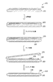
図5に示すのは、ハンドル基板上にドナー薄膜を備えた貼り合わせ基板の製造方法である。まず、ハンドル基板103上にイオン注入・剥離法によって貼り合わせ層102を形成する。この際、貼り合わせ層102の表面には0.15um程度の剥離ダメージ層が形成されている。ついで、貼り合わせ層102の表面を保護部材105で被覆する。ハンドル基板表面107にサンドブラスト処理を施し、保護部材105を剥離する。この後で、剥離ダメージ層を除去するために、貼り合わせ層表面を化学エッチングして前記ドナー薄膜109を形成する。この過程で、ドナー薄膜109の表面には、微小な欠陥108が形成されている。
本発明者らが鋭意検討した結果、保護テープに由来する有機物残渣106が貼り合わせ層102の表面に残存した場合に次のエッチング工程で、エッチング溶液と有機物残渣との組み合わせにより、貼り合わせ層102が局部的に選択的に早くエッチングされ、これらの微小な欠陥108が発生することを突き止めた。アルカリ溶液には有機物残渣106を除去する能力はあるものの、完全に除去される前にシリコン層にボイドを残すことが判明した。
図5に示すのは、ハンドル基板上にドナー薄膜を備えた貼り合わせ基板の製造方法である。まず、ハンドル基板103上にイオン注入・剥離法によって貼り合わせ層102を形成する。この際、貼り合わせ層102の表面には0.15um程度の剥離ダメージ層が形成されている。ついで、貼り合わせ層102の表面を保護部材105で被覆する。ハンドル基板表面107にサンドブラスト処理を施し、保護部材105を剥離する。この後で、剥離ダメージ層を除去するために、貼り合わせ層表面を化学エッチングして前記ドナー薄膜109を形成する。この過程で、ドナー薄膜109の表面には、微小な欠陥108が形成されている。
本発明者らが鋭意検討した結果、保護テープに由来する有機物残渣106が貼り合わせ層102の表面に残存した場合に次のエッチング工程で、エッチング溶液と有機物残渣との組み合わせにより、貼り合わせ層102が局部的に選択的に早くエッチングされ、これらの微小な欠陥108が発生することを突き止めた。アルカリ溶液には有機物残渣106を除去する能力はあるものの、完全に除去される前にシリコン層にボイドを残すことが判明した。
図1に、上記検討結果に基づいて開発された本発明の貼り合わせ基板の製造方法の一連の工程を示す。
本発明の貼り合わせ基板の製造方法は、ハンドル基板上に貼り合わせ層を形成した直後の基板、特に薄膜転写後のSOQ,SOG,SOS基板等に好適に適用できる。したがって、ハンドル基板は、石英、ガラス、または、サファイアであることが好ましく、貼り合わせ層は、シリコン層であることが好ましい。
本発明の貼り合わせ基板の製造方法は、ハンドル基板上に貼り合わせ層を形成した直後の基板、特に薄膜転写後のSOQ,SOG,SOS基板等に好適に適用できる。したがって、ハンドル基板は、石英、ガラス、または、サファイアであることが好ましく、貼り合わせ層は、シリコン層であることが好ましい。
ハンドル基板上に貼り合わせ層を形成する方法としては、イオン注入・剥離法が挙げられる。
イオン注入・剥離法は、例えば、ドナー基板または表面に酸化膜を形成したドナー基板に、表面から水素イオンまたは希ガスイオンあるいはこれらの両方を注入してイオン注入層を形成し、前記ドナー基板または表面に酸化膜を形成したドナー基板のイオン注入した面と、ハンドル基板の1表面とを、表面活性化処理を施したうえで密着させて貼り合わせ、前記イオン注入層を境界として、前記ドナー基板または表面に酸化膜を形成したシリコン基板を剥離して薄膜化することにより行う。
なお、上記イオン注入・剥離法で貼り合わせ層を形成する際に、予め裏面を粗面化したハンドル基板を用いることも考えられるが、該剥離時の応力が局所的に異なることで、転写されたドナー薄膜の膜厚がばらつくために望ましくはない。特に、剥離の際に補剛板を裏面に密着させて剥離速度を制御する場合には、補剛板との密着力が局所的に異なることで、剥離時の応力が局所的に異なり、同様に転写されたシリコンの膜厚がばらつく虞があるからである。
したがって、ハンドル基板としては、予め両面研磨したものを用いることが好ましく、貼り合わせ層を形成した後に後述のサンドブラスト処理を施すことが好ましい。
さらには貼り合わせ時に粗面からの異物が貼り合わせ面に入り込み、剥離時にボイドと呼ばれる未転写欠陥を引き起こす可能性があるために、貼り合わせ前の粗面化は望ましくない。
イオン注入・剥離法は、例えば、ドナー基板または表面に酸化膜を形成したドナー基板に、表面から水素イオンまたは希ガスイオンあるいはこれらの両方を注入してイオン注入層を形成し、前記ドナー基板または表面に酸化膜を形成したドナー基板のイオン注入した面と、ハンドル基板の1表面とを、表面活性化処理を施したうえで密着させて貼り合わせ、前記イオン注入層を境界として、前記ドナー基板または表面に酸化膜を形成したシリコン基板を剥離して薄膜化することにより行う。
なお、上記イオン注入・剥離法で貼り合わせ層を形成する際に、予め裏面を粗面化したハンドル基板を用いることも考えられるが、該剥離時の応力が局所的に異なることで、転写されたドナー薄膜の膜厚がばらつくために望ましくはない。特に、剥離の際に補剛板を裏面に密着させて剥離速度を制御する場合には、補剛板との密着力が局所的に異なることで、剥離時の応力が局所的に異なり、同様に転写されたシリコンの膜厚がばらつく虞があるからである。
したがって、ハンドル基板としては、予め両面研磨したものを用いることが好ましく、貼り合わせ層を形成した後に後述のサンドブラスト処理を施すことが好ましい。
さらには貼り合わせ時に粗面からの異物が貼り合わせ面に入り込み、剥離時にボイドと呼ばれる未転写欠陥を引き起こす可能性があるために、貼り合わせ前の粗面化は望ましくない。
次に、貼り合わせ層の表面を保護部材で被覆する(S2)。ドナー薄膜の表面がサンドブラスト処理を受けないようにするためである。この際、予め有機膜等を塗布することは不要であり、工程は簡略化される。
前記保護部材としては、バックグラインド用保護テープ、ダイシング用テープ、または、ダイボンディングテープであることが好ましい。
前記保護部材としては、バックグラインド用保護テープ、ダイシング用テープ、または、ダイボンディングテープであることが好ましい。
次に、ハンドル基板表面にサンドブラスト処理(S3)を行う。サンドブラスト処理で粗面化することにより搬送及び載置時後の取り外しが容易になり、更に透明絶縁性基板をハンドル基板とする貼り合わせ基板では、シリコン半導体ウエーハの工程と同じく、表面の識別が簡便なものとすることができる。
サンドブラスト面に対しては、必要に応じてHFを含む溶液等で洗浄(S4)を行う。粉末が残存していると貼り合わせ層の表面を汚染する虞があるからである。上記洗浄により、サンドブラスト処理を施した裏面の凹凸からの発塵を効果的に抑制し、パーティクル汚染が発生するのを抑制できる。
次に、保護部材を剥離する(S5)。保護部材を剥離する方法としては、特に限定されないが、UV硬化テープを用いる場合は、UV硬化処理が挙げられる。
本発明の貼り合わせ基板の製造方法では、ここで、貼り合わせ層の表面に対して、エッチング作用が無い洗浄を施す工程(S6)を含む。
洗浄方法としては、UVドライ洗浄、UVオゾン洗浄、硫酸洗浄、硫酸過水の少なくともいずれか1つを含むことが好ましく、2種以上の洗浄方法(SPM)洗浄、または、プラズマ洗浄(アッシング)を用いることも可能である。
なお、プラズマ洗浄を行う場合、その雰囲気は、酸素、アルゴンおよび窒素からなる群より選択される1種または2種以上の混合ガスであることが好ましい。
洗浄方法としては、UVドライ洗浄、UVオゾン洗浄、硫酸洗浄、硫酸過水の少なくともいずれか1つを含むことが好ましく、2種以上の洗浄方法(SPM)洗浄、または、プラズマ洗浄(アッシング)を用いることも可能である。
なお、プラズマ洗浄を行う場合、その雰囲気は、酸素、アルゴンおよび窒素からなる群より選択される1種または2種以上の混合ガスであることが好ましい。
次いで、貼り合わせ層の表面の剥離ダメージ層を取り除くために、化学エッチング(S7)を行い、ドナー薄膜を形成する。
前記化学エッチングに用いるエッチング溶液としては、アンモニア過水、アンモニア、KOH、NaOH、CsOH、TMAH、EDPおよびヒドラジンからなる群より選択される1種または2種以上の組み合わせであることが好ましい。
ドナー薄膜の最終的な膜厚としては、特に限定はされないが50nm~500nmとすることができる。一般的に有機溶剤はアルカリ溶液を比較するとエッチング速度が遅いので、正確なエッチング量制御が必要な際には適している。
前記化学エッチングに用いるエッチング溶液としては、アンモニア過水、アンモニア、KOH、NaOH、CsOH、TMAH、EDPおよびヒドラジンからなる群より選択される1種または2種以上の組み合わせであることが好ましい。
ドナー薄膜の最終的な膜厚としては、特に限定はされないが50nm~500nmとすることができる。一般的に有機溶剤はアルカリ溶液を比較するとエッチング速度が遅いので、正確なエッチング量制御が必要な際には適している。
これらのようにすれば、石英、ガラス、サファイア等の絶縁性基板の表面上にシリコン等のドナー薄膜を形成した異種物質の貼り合わせ基板を準備することができるとともに、TFT-LCDや高周波(RF)デバイス、その他MEMS製品等の用途に適したものとなる。
まず、ハンドル基板として両面研磨された150mmの石英基板(信越化学工業社製、厚さ625um)を準備した。
次にドナー基板として、径150mm、酸化膜を200nm成長させて単結晶シリコン基板(信越化学工業社製)を準備した。該シリコン基板のハンドル基板との貼り合わせ面について、水素イオンを注入し、イオン注入層を形成した。イオン注入条件は、注入エネルギーを55keVとした。
次に、プラズマ処理装置を用い、プラズマ用ガスとして窒素ガスを導入し、準備したシリコン基板のイオン注入面、ならびに、石英基板の1面に表面活性化処理を施した。
そして、これらの基板を室温で貼り合わせ、300℃で30分間熱処理を行った後、貼り合わせ界面付近に機械的衝撃を加えることにより、イオン注入層を境界としてシリコン基板の一部を剥離し、石英基板の表面上にシリコン薄膜を形成したSOQ基板を形成した。
剥離直後のSOQ基板(口径150mm、厚さ625um、シリコン層厚さ400nm)を複数枚作製し、それぞれにダイシングテープ(品番:D636、リンテック社製)を被覆し、石英基板側の表面にサンドブラスト処理を施した。その後、2%フッ酸にウェーハを浸漬し洗浄を行い、乾燥の後、UV硬化を施しテープを剥がした。
ついで、以下の処理を別々のウェーハに対して施した。
(1)未処理
(2)UVドライ洗浄(5分)
(3)UVオゾン洗浄(5分)
(4)熱濃硫酸(98%、80℃、5分)
(5)硫酸過水洗浄(H2SO4:H2O2=4:1 、5分)
(6)O2プラズマ洗浄(アッシング処理:5分)
(7)Arプラズマ処理(5分)
次にドナー基板として、径150mm、酸化膜を200nm成長させて単結晶シリコン基板(信越化学工業社製)を準備した。該シリコン基板のハンドル基板との貼り合わせ面について、水素イオンを注入し、イオン注入層を形成した。イオン注入条件は、注入エネルギーを55keVとした。
次に、プラズマ処理装置を用い、プラズマ用ガスとして窒素ガスを導入し、準備したシリコン基板のイオン注入面、ならびに、石英基板の1面に表面活性化処理を施した。
そして、これらの基板を室温で貼り合わせ、300℃で30分間熱処理を行った後、貼り合わせ界面付近に機械的衝撃を加えることにより、イオン注入層を境界としてシリコン基板の一部を剥離し、石英基板の表面上にシリコン薄膜を形成したSOQ基板を形成した。
剥離直後のSOQ基板(口径150mm、厚さ625um、シリコン層厚さ400nm)を複数枚作製し、それぞれにダイシングテープ(品番:D636、リンテック社製)を被覆し、石英基板側の表面にサンドブラスト処理を施した。その後、2%フッ酸にウェーハを浸漬し洗浄を行い、乾燥の後、UV硬化を施しテープを剥がした。
ついで、以下の処理を別々のウェーハに対して施した。
(1)未処理
(2)UVドライ洗浄(5分)
(3)UVオゾン洗浄(5分)
(4)熱濃硫酸(98%、80℃、5分)
(5)硫酸過水洗浄(H2SO4:H2O2=4:1 、5分)
(6)O2プラズマ洗浄(アッシング処理:5分)
(7)Arプラズマ処理(5分)
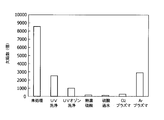
これらの処理の後にエッチングにより、120nmのシリコン層を除去し、続いて50nmの研磨(CMP研磨)を行った。エッチングに用いたアルカリ溶液は、SC1溶液とし、過酸化水素水の量を故意に減らし、エッチング効果を高めたものである。組成は、NH4OH:H2O2:H2O = 1:0.2:10であり処理温度は80℃とした。この後に検査のためにウェーハを10%HF溶液に10分浸漬し、ボイド欠陥を通じて下地の石英層をエッチングすることで欠陥を見やすくした後に欠陥検査装置を用い、0.2μm以上の欠陥数を数えた。結果を図2に示す。この図より、程度の差はあるものの(2)~(7)の対策が功を奏していることがわかった。
実施例1と同様の実験を行った。エッチング溶液のみを変更し、TMAH(Tetramethyl ammonium hydroxide)溶液を用い、120nmのシリコン層を除去し、続いて50nmの研磨(CMP研磨)を行った。検査のためにウェーハを10%HF溶液に10分浸漬し、ボイド欠陥を通じて下地の石英層をエッチングすることで欠陥を見やすくした後に欠陥検査装置を用い、欠陥数を数えた。結果を図3に示す。欠陥数は実施例1と多少異なるものの、傾向としては実施例1と同じであることが判明した。この結果から、用いるエッチング溶液には影響されないことが示唆された。
Claims (7)
- ハンドル基板上にドナー薄膜を備えた貼り合わせ基板の製造方法であって、
前記ハンドル基板上にイオン注入・剥離法によって貼り合わせ層を形成する工程と、
前記貼り合わせ層の表面を保護部材で被覆する工程と、
前記ハンドル基板の表面にサンドブラスト処理を施す工程と、
前記保護部材を剥離する工程と、
前記保護部材を剥離した後の貼り合わせ層の表面に対してエッチング作用が無い洗浄を施す工程と、
前記洗浄工程の後に貼り合わせ層表面を化学エッチングして前記ドナー薄膜を形成する工程とを含む貼り合わせ基板の製造方法。 - 前記貼り合わせ層の保護部材による被覆に先立ち、有機膜の塗布が不要であって、かつ、前記エッチング作用が無い洗浄が、UVドライ洗浄、UVオゾン洗浄、硫酸洗浄、硫酸過水洗浄およびプラズマ洗浄からなる群より選択される1つまたは2つ以上の方法による洗浄を含むことを特徴とする請求項1に記載の貼り合わせ基板の製造方法。
- 前記プラズマ洗浄の雰囲気が、酸素、アルゴンおよび窒素からなる群より選択される1種または2種以上の混合ガスであることを特徴とする請求項2に記載の貼り合わせ基板の製造方法。
- 前記保護部材が、バックグラインド用保護テープ、ダイシング用テープ、または、ダイボンディングテープであることを特徴とする請求項1または2に記載の貼り合わせ基板の製造方法。
- 前記化学エッチングに用いるエッチング溶液が、アンモニア過水、アンモニア、KOH、NaOH、CsOH、TMAH、EDPおよびヒドラジンからなる群より選択される1種または2種以上の組み合わせであることを特徴とする請求項1または2に記載の貼り合わせ基板の製造方法。
- 前記ハンドル基板が、石英、ガラス、または、サファイアであることを特徴とする請求項1または2に記載の貼り合わせ基板の製造方法。
- 前記サンドブラスト処理の後に、HFを含む溶液でサンドブラスト面を洗浄してから保護テープを剥がすことを特徴とする請求項1または2に記載の貼り合わせ基板の製造方法。
Applications Claiming Priority (2)
| Application Number | Priority Date | Filing Date | Title |
|---|---|---|---|
| JP2009-133342 | 2009-06-02 | ||
| JP2009133342A JP5335564B2 (ja) | 2009-06-02 | 2009-06-02 | サンドブラスト処理を施した貼り合わせ基板の結晶品質改善方法 |
Publications (1)
| Publication Number | Publication Date |
|---|---|
| WO2010140510A1 true WO2010140510A1 (ja) | 2010-12-09 |
Family
ID=43297646
Family Applications (1)
| Application Number | Title | Priority Date | Filing Date |
|---|---|---|---|
| PCT/JP2010/058827 Ceased WO2010140510A1 (ja) | 2009-06-02 | 2010-05-25 | サンドブラスト処理を施した貼り合わせ基板の結晶品質改善方法 |
Country Status (2)
| Country | Link |
|---|---|
| JP (1) | JP5335564B2 (ja) |
| WO (1) | WO2010140510A1 (ja) |
Cited By (1)
| Publication number | Priority date | Publication date | Assignee | Title |
|---|---|---|---|---|
| CN113414193A (zh) * | 2021-07-09 | 2021-09-21 | 百腾科技(苏州)有限公司 | 一种pc膜的剥离方法 |
Citations (4)
| Publication number | Priority date | Publication date | Assignee | Title |
|---|---|---|---|---|
| JPH04162630A (ja) * | 1990-10-25 | 1992-06-08 | Mitsubishi Materials Shilicon Corp | 半導体基板 |
| JP2003224247A (ja) * | 2002-01-29 | 2003-08-08 | Shin Etsu Handotai Co Ltd | Soiウエーハ及びsoiウエーハの製造方法 |
| JP2006294957A (ja) * | 2005-04-13 | 2006-10-26 | Shin Etsu Handotai Co Ltd | 貼り合わせsoiウエーハの製造方法及び貼り合わせsoiウエーハ |
| JP2008288556A (ja) * | 2007-04-18 | 2008-11-27 | Shin Etsu Chem Co Ltd | 貼り合わせ基板の製造方法 |
-
2009
- 2009-06-02 JP JP2009133342A patent/JP5335564B2/ja active Active
-
2010
- 2010-05-25 WO PCT/JP2010/058827 patent/WO2010140510A1/ja not_active Ceased
Patent Citations (4)
| Publication number | Priority date | Publication date | Assignee | Title |
|---|---|---|---|---|
| JPH04162630A (ja) * | 1990-10-25 | 1992-06-08 | Mitsubishi Materials Shilicon Corp | 半導体基板 |
| JP2003224247A (ja) * | 2002-01-29 | 2003-08-08 | Shin Etsu Handotai Co Ltd | Soiウエーハ及びsoiウエーハの製造方法 |
| JP2006294957A (ja) * | 2005-04-13 | 2006-10-26 | Shin Etsu Handotai Co Ltd | 貼り合わせsoiウエーハの製造方法及び貼り合わせsoiウエーハ |
| JP2008288556A (ja) * | 2007-04-18 | 2008-11-27 | Shin Etsu Chem Co Ltd | 貼り合わせ基板の製造方法 |
Cited By (1)
| Publication number | Priority date | Publication date | Assignee | Title |
|---|---|---|---|---|
| CN113414193A (zh) * | 2021-07-09 | 2021-09-21 | 百腾科技(苏州)有限公司 | 一种pc膜的剥离方法 |
Also Published As
| Publication number | Publication date |
|---|---|
| JP5335564B2 (ja) | 2013-11-06 |
| JP2010283033A (ja) | 2010-12-16 |
Similar Documents
| Publication | Publication Date | Title |
|---|---|---|
| JP5274859B2 (ja) | 貼り合わせ基板の製造方法 | |
| US8088670B2 (en) | Method for manufacturing bonded substrate with sandblast treatment | |
| KR101541940B1 (ko) | Soi 기판의 제조 방법 | |
| KR100769327B1 (ko) | 두 웨이퍼 결합에 선행되는 열처리 | |
| JP5030992B2 (ja) | サンドブラスト処理された裏面を有するsoi基板の製造方法 | |
| JP5292642B2 (ja) | 層の貼り合わせおよび転写プロセス | |
| JP2013522896A (ja) | セミコンダクタオンインシュレータ型の基板の仕上げ処理方法 | |
| JP5780234B2 (ja) | Soiウェーハの製造方法 | |
| US9922867B2 (en) | Method for transferring a useful layer | |
| EP2924736B1 (en) | Method for manufacturing soi wafer | |
| JP5335564B2 (ja) | サンドブラスト処理を施した貼り合わせ基板の結晶品質改善方法 | |
| JP5443819B2 (ja) | 粗面化された基板の製造方法 | |
| TW201005883A (en) | Method for manufacturing soi wafer | |
| JP5364345B2 (ja) | Soi基板の作製方法 | |
| JP5368000B2 (ja) | Soi基板の製造方法 | |
| JP5135713B2 (ja) | 半導体基板の製造方法 | |
| JP2009252948A (ja) | 貼り合わせウェーハの製造方法 |
Legal Events
| Date | Code | Title | Description |
|---|---|---|---|
| 121 | Ep: the epo has been informed by wipo that ep was designated in this application |
Ref document number: 10783294 Country of ref document: EP Kind code of ref document: A1 |
|
| NENP | Non-entry into the national phase |
Ref country code: DE |
|
| 122 | Ep: pct application non-entry in european phase |
Ref document number: 10783294 Country of ref document: EP Kind code of ref document: A1 |