WO2010140278A1 - Semiconductor device and process for manufacture thereof - Google Patents
Semiconductor device and process for manufacture thereof Download PDFInfo
- Publication number
- WO2010140278A1 WO2010140278A1 PCT/JP2010/000103 JP2010000103W WO2010140278A1 WO 2010140278 A1 WO2010140278 A1 WO 2010140278A1 JP 2010000103 W JP2010000103 W JP 2010000103W WO 2010140278 A1 WO2010140278 A1 WO 2010140278A1
- Authority
- WO
- WIPO (PCT)
- Prior art keywords
- film
- high dielectric
- dielectric material
- semiconductor device
- hafnium
- Prior art date
Links
- 239000004065 semiconductor Substances 0.000 title claims abstract description 89
- 238000000034 method Methods 0.000 title claims description 24
- 238000004519 manufacturing process Methods 0.000 title claims description 22
- IJGRMHOSHXDMSA-UHFFFAOYSA-N Atomic nitrogen Chemical compound N#N IJGRMHOSHXDMSA-UHFFFAOYSA-N 0.000 claims abstract description 156
- 229910052757 nitrogen Inorganic materials 0.000 claims abstract description 78
- 239000000758 substrate Substances 0.000 claims abstract description 40
- 239000003989 dielectric material Substances 0.000 claims description 84
- 239000007789 gas Substances 0.000 claims description 54
- 229910052735 hafnium Inorganic materials 0.000 claims description 45
- VBJZVLUMGGDVMO-UHFFFAOYSA-N hafnium atom Chemical compound [Hf] VBJZVLUMGGDVMO-UHFFFAOYSA-N 0.000 claims description 45
- 229910052760 oxygen Inorganic materials 0.000 claims description 45
- QVGXLLKOCUKJST-UHFFFAOYSA-N atomic oxygen Chemical compound [O] QVGXLLKOCUKJST-UHFFFAOYSA-N 0.000 claims description 44
- 239000001301 oxygen Substances 0.000 claims description 44
- 239000007800 oxidant agent Substances 0.000 claims description 31
- 229910052751 metal Inorganic materials 0.000 claims description 21
- 239000002184 metal Substances 0.000 claims description 21
- 230000001590 oxidative effect Effects 0.000 claims description 17
- CBENFWSGALASAD-UHFFFAOYSA-N Ozone Chemical compound [O-][O+]=O CBENFWSGALASAD-UHFFFAOYSA-N 0.000 claims description 6
- 229910052782 aluminium Inorganic materials 0.000 claims description 4
- PDPJQWYGJJBYLF-UHFFFAOYSA-J hafnium tetrachloride Chemical compound Cl[Hf](Cl)(Cl)Cl PDPJQWYGJJBYLF-UHFFFAOYSA-J 0.000 claims description 4
- 229910052746 lanthanum Inorganic materials 0.000 claims description 4
- 229910052715 tantalum Inorganic materials 0.000 claims description 4
- 229910052719 titanium Inorganic materials 0.000 claims description 4
- XLYOFNOQVPJJNP-UHFFFAOYSA-N water Substances O XLYOFNOQVPJJNP-UHFFFAOYSA-N 0.000 claims description 4
- 229910052727 yttrium Inorganic materials 0.000 claims description 4
- 229910052726 zirconium Inorganic materials 0.000 claims description 4
- 150000002739 metals Chemical class 0.000 claims description 2
- 229910004129 HfSiO Inorganic materials 0.000 description 58
- XUIMIQQOPSSXEZ-UHFFFAOYSA-N Silicon Chemical compound [Si] XUIMIQQOPSSXEZ-UHFFFAOYSA-N 0.000 description 25
- 229910052710 silicon Inorganic materials 0.000 description 25
- 239000010703 silicon Substances 0.000 description 25
- 238000010438 heat treatment Methods 0.000 description 12
- VYPSYNLAJGMNEJ-UHFFFAOYSA-N Silicium dioxide Chemical compound O=[Si]=O VYPSYNLAJGMNEJ-UHFFFAOYSA-N 0.000 description 10
- 229910052814 silicon oxide Inorganic materials 0.000 description 10
- 229910021420 polycrystalline silicon Inorganic materials 0.000 description 9
- 229920005591 polysilicon Polymers 0.000 description 9
- 239000000463 material Substances 0.000 description 6
- 238000005191 phase separation Methods 0.000 description 6
- ZAMOUSCENKQFHK-UHFFFAOYSA-N Chlorine atom Chemical compound [Cl] ZAMOUSCENKQFHK-UHFFFAOYSA-N 0.000 description 5
- 239000000460 chlorine Substances 0.000 description 5
- 229910052801 chlorine Inorganic materials 0.000 description 5
- 238000002425 crystallisation Methods 0.000 description 5
- 230000008025 crystallization Effects 0.000 description 5
- 239000012535 impurity Substances 0.000 description 5
- 230000007547 defect Effects 0.000 description 4
- 230000006866 deterioration Effects 0.000 description 4
- 238000009413 insulation Methods 0.000 description 4
- ZOXJGFHDIHLPTG-UHFFFAOYSA-N Boron Chemical compound [B] ZOXJGFHDIHLPTG-UHFFFAOYSA-N 0.000 description 3
- OAICVXFJPJFONN-UHFFFAOYSA-N Phosphorus Chemical compound [P] OAICVXFJPJFONN-UHFFFAOYSA-N 0.000 description 3
- 229910003902 SiCl 4 Inorganic materials 0.000 description 3
- ATJFFYVFTNAWJD-UHFFFAOYSA-N Tin Chemical compound [Sn] ATJFFYVFTNAWJD-UHFFFAOYSA-N 0.000 description 3
- 229910052796 boron Inorganic materials 0.000 description 3
- 239000003990 capacitor Substances 0.000 description 3
- 239000012299 nitrogen atmosphere Substances 0.000 description 3
- QJGQUHMNIGDVPM-UHFFFAOYSA-N nitrogen group Chemical group [N] QJGQUHMNIGDVPM-UHFFFAOYSA-N 0.000 description 3
- NFHFRUOZVGFOOS-UHFFFAOYSA-N palladium;triphenylphosphane Chemical compound [Pd].C1=CC=CC=C1P(C=1C=CC=CC=1)C1=CC=CC=C1.C1=CC=CC=C1P(C=1C=CC=CC=1)C1=CC=CC=C1.C1=CC=CC=C1P(C=1C=CC=CC=1)C1=CC=CC=C1.C1=CC=CC=C1P(C=1C=CC=CC=1)C1=CC=CC=C1 NFHFRUOZVGFOOS-UHFFFAOYSA-N 0.000 description 3
- 229910052698 phosphorus Inorganic materials 0.000 description 3
- 239000011574 phosphorus Substances 0.000 description 3
- 229910021332 silicide Inorganic materials 0.000 description 3
- FVBUAEGBCNSCDD-UHFFFAOYSA-N silicide(4-) Chemical compound [Si-4] FVBUAEGBCNSCDD-UHFFFAOYSA-N 0.000 description 3
- ITWBWJFEJCHKSN-UHFFFAOYSA-N 1,4,7-triazonane Chemical compound C1CNCCNCCN1 ITWBWJFEJCHKSN-UHFFFAOYSA-N 0.000 description 2
- OKTJSMMVPCPJKN-UHFFFAOYSA-N Carbon Chemical compound [C] OKTJSMMVPCPJKN-UHFFFAOYSA-N 0.000 description 2
- 229910010037 TiAlN Inorganic materials 0.000 description 2
- 229910052785 arsenic Inorganic materials 0.000 description 2
- RQNWIZPPADIBDY-UHFFFAOYSA-N arsenic atom Chemical compound [As] RQNWIZPPADIBDY-UHFFFAOYSA-N 0.000 description 2
- 238000000231 atomic layer deposition Methods 0.000 description 2
- 229910052799 carbon Inorganic materials 0.000 description 2
- 238000000151 deposition Methods 0.000 description 2
- 239000012528 membrane Substances 0.000 description 2
- 125000004433 nitrogen atom Chemical group N* 0.000 description 2
- -1 1-methoxy-2-methyl-2-propoxy Chemical group 0.000 description 1
- VXEGSRKPIUDPQT-UHFFFAOYSA-N 4-[4-(4-methoxyphenyl)piperazin-1-yl]aniline Chemical compound C1=CC(OC)=CC=C1N1CCN(C=2C=CC(N)=CC=2)CC1 VXEGSRKPIUDPQT-UHFFFAOYSA-N 0.000 description 1
- 229910018072 Al 2 O 3 Inorganic materials 0.000 description 1
- IUBCUJZHRZSKDG-UHFFFAOYSA-N C(C)N(C)[Hf] Chemical compound C(C)N(C)[Hf] IUBCUJZHRZSKDG-UHFFFAOYSA-N 0.000 description 1
- OEZJRMFFFWXQJL-UHFFFAOYSA-N COCC(C)(O[Hf])C Chemical compound COCC(C)(O[Hf])C OEZJRMFFFWXQJL-UHFFFAOYSA-N 0.000 description 1
- 235000012093 Myrtus ugni Nutrition 0.000 description 1
- BPQQTUXANYXVAA-UHFFFAOYSA-N Orthosilicate Chemical compound [O-][Si]([O-])([O-])[O-] BPQQTUXANYXVAA-UHFFFAOYSA-N 0.000 description 1
- 244000061461 Tema Species 0.000 description 1
- 238000004833 X-ray photoelectron spectroscopy Methods 0.000 description 1
- 230000003213 activating effect Effects 0.000 description 1
- 150000004645 aluminates Chemical class 0.000 description 1
- PNEYBMLMFCGWSK-UHFFFAOYSA-N aluminium oxide Inorganic materials [O-2].[O-2].[O-2].[Al+3].[Al+3] PNEYBMLMFCGWSK-UHFFFAOYSA-N 0.000 description 1
- 239000012298 atmosphere Substances 0.000 description 1
- 125000004429 atom Chemical group 0.000 description 1
- 230000004888 barrier function Effects 0.000 description 1
- 238000005229 chemical vapour deposition Methods 0.000 description 1
- 239000013078 crystal Substances 0.000 description 1
- 230000008021 deposition Effects 0.000 description 1
- 238000003795 desorption Methods 0.000 description 1
- 230000002542 deteriorative effect Effects 0.000 description 1
- 238000009792 diffusion process Methods 0.000 description 1
- 230000000694 effects Effects 0.000 description 1
- 230000005684 electric field Effects 0.000 description 1
- 238000001941 electron spectroscopy Methods 0.000 description 1
- 230000005669 field effect Effects 0.000 description 1
- 229910000449 hafnium oxide Inorganic materials 0.000 description 1
- WIHZLLGSGQNAGK-UHFFFAOYSA-N hafnium(4+);oxygen(2-) Chemical compound [O-2].[O-2].[Hf+4] WIHZLLGSGQNAGK-UHFFFAOYSA-N 0.000 description 1
- MZCHLVMRAOQSDA-UHFFFAOYSA-N hafnium;1-methoxy-2-methylpropan-2-ol Chemical compound [Hf].COCC(C)(C)O.COCC(C)(C)O.COCC(C)(C)O.COCC(C)(C)O MZCHLVMRAOQSDA-UHFFFAOYSA-N 0.000 description 1
- 230000001678 irradiating effect Effects 0.000 description 1
- 229910044991 metal oxide Inorganic materials 0.000 description 1
- 150000004706 metal oxides Chemical class 0.000 description 1
- 238000002156 mixing Methods 0.000 description 1
- 238000005121 nitriding Methods 0.000 description 1
- 230000003647 oxidation Effects 0.000 description 1
- 238000007254 oxidation reaction Methods 0.000 description 1
- RVTZCBVAJQQJTK-UHFFFAOYSA-N oxygen(2-);zirconium(4+) Chemical compound [O-2].[O-2].[Zr+4] RVTZCBVAJQQJTK-UHFFFAOYSA-N 0.000 description 1
- 230000000149 penetrating effect Effects 0.000 description 1
- 230000035515 penetration Effects 0.000 description 1
- 229910001404 rare earth metal oxide Inorganic materials 0.000 description 1
- 239000000523 sample Substances 0.000 description 1
- 238000000926 separation method Methods 0.000 description 1
- 239000005049 silicon tetrachloride Substances 0.000 description 1
- 238000001947 vapour-phase growth Methods 0.000 description 1
- 229910001928 zirconium oxide Inorganic materials 0.000 description 1
Images
Classifications
-
- H—ELECTRICITY
- H01—ELECTRIC ELEMENTS
- H01L—SEMICONDUCTOR DEVICES NOT COVERED BY CLASS H10
- H01L21/00—Processes or apparatus adapted for the manufacture or treatment of semiconductor or solid state devices or of parts thereof
- H01L21/02—Manufacture or treatment of semiconductor devices or of parts thereof
- H01L21/04—Manufacture or treatment of semiconductor devices or of parts thereof the devices having at least one potential-jump barrier or surface barrier, e.g. PN junction, depletion layer or carrier concentration layer
- H01L21/18—Manufacture or treatment of semiconductor devices or of parts thereof the devices having at least one potential-jump barrier or surface barrier, e.g. PN junction, depletion layer or carrier concentration layer the devices having semiconductor bodies comprising elements of Group IV of the Periodic System or AIIIBV compounds with or without impurities, e.g. doping materials
- H01L21/28—Manufacture of electrodes on semiconductor bodies using processes or apparatus not provided for in groups H01L21/20 - H01L21/268
- H01L21/28008—Making conductor-insulator-semiconductor electrodes
- H01L21/28017—Making conductor-insulator-semiconductor electrodes the insulator being formed after the semiconductor body, the semiconductor being silicon
- H01L21/28158—Making the insulator
- H01L21/28167—Making the insulator on single crystalline silicon, e.g. using a liquid, i.e. chemical oxidation
- H01L21/28202—Making the insulator on single crystalline silicon, e.g. using a liquid, i.e. chemical oxidation in a nitrogen-containing ambient, e.g. nitride deposition, growth, oxynitridation, NH3 nitridation, N2O oxidation, thermal nitridation, RTN, plasma nitridation, RPN
-
- H—ELECTRICITY
- H01—ELECTRIC ELEMENTS
- H01L—SEMICONDUCTOR DEVICES NOT COVERED BY CLASS H10
- H01L21/00—Processes or apparatus adapted for the manufacture or treatment of semiconductor or solid state devices or of parts thereof
- H01L21/02—Manufacture or treatment of semiconductor devices or of parts thereof
- H01L21/02104—Forming layers
- H01L21/02107—Forming insulating materials on a substrate
- H01L21/02109—Forming insulating materials on a substrate characterised by the type of layer, e.g. type of material, porous/non-porous, pre-cursors, mixtures or laminates
- H01L21/02112—Forming insulating materials on a substrate characterised by the type of layer, e.g. type of material, porous/non-porous, pre-cursors, mixtures or laminates characterised by the material of the layer
- H01L21/02123—Forming insulating materials on a substrate characterised by the type of layer, e.g. type of material, porous/non-porous, pre-cursors, mixtures or laminates characterised by the material of the layer the material containing silicon
- H01L21/02142—Forming insulating materials on a substrate characterised by the type of layer, e.g. type of material, porous/non-porous, pre-cursors, mixtures or laminates characterised by the material of the layer the material containing silicon the material containing silicon and at least one metal element, e.g. metal silicate based insulators or metal silicon oxynitrides
- H01L21/02148—Forming insulating materials on a substrate characterised by the type of layer, e.g. type of material, porous/non-porous, pre-cursors, mixtures or laminates characterised by the material of the layer the material containing silicon the material containing silicon and at least one metal element, e.g. metal silicate based insulators or metal silicon oxynitrides the material containing hafnium, e.g. HfSiOx or HfSiON
-
- H—ELECTRICITY
- H01—ELECTRIC ELEMENTS
- H01L—SEMICONDUCTOR DEVICES NOT COVERED BY CLASS H10
- H01L21/00—Processes or apparatus adapted for the manufacture or treatment of semiconductor or solid state devices or of parts thereof
- H01L21/02—Manufacture or treatment of semiconductor devices or of parts thereof
- H01L21/02104—Forming layers
- H01L21/02107—Forming insulating materials on a substrate
- H01L21/02225—Forming insulating materials on a substrate characterised by the process for the formation of the insulating layer
- H01L21/0226—Forming insulating materials on a substrate characterised by the process for the formation of the insulating layer formation by a deposition process
- H01L21/02263—Forming insulating materials on a substrate characterised by the process for the formation of the insulating layer formation by a deposition process deposition from the gas or vapour phase
- H01L21/02271—Forming insulating materials on a substrate characterised by the process for the formation of the insulating layer formation by a deposition process deposition from the gas or vapour phase deposition by decomposition or reaction of gaseous or vapour phase compounds, i.e. chemical vapour deposition
-
- H—ELECTRICITY
- H01—ELECTRIC ELEMENTS
- H01L—SEMICONDUCTOR DEVICES NOT COVERED BY CLASS H10
- H01L21/00—Processes or apparatus adapted for the manufacture or treatment of semiconductor or solid state devices or of parts thereof
- H01L21/02—Manufacture or treatment of semiconductor devices or of parts thereof
- H01L21/02104—Forming layers
- H01L21/02107—Forming insulating materials on a substrate
- H01L21/02296—Forming insulating materials on a substrate characterised by the treatment performed before or after the formation of the layer
- H01L21/02318—Forming insulating materials on a substrate characterised by the treatment performed before or after the formation of the layer post-treatment
- H01L21/02321—Forming insulating materials on a substrate characterised by the treatment performed before or after the formation of the layer post-treatment introduction of substances into an already existing insulating layer
- H01L21/02329—Forming insulating materials on a substrate characterised by the treatment performed before or after the formation of the layer post-treatment introduction of substances into an already existing insulating layer introduction of nitrogen
- H01L21/02332—Forming insulating materials on a substrate characterised by the treatment performed before or after the formation of the layer post-treatment introduction of substances into an already existing insulating layer introduction of nitrogen into an oxide layer, e.g. changing SiO to SiON
-
- H—ELECTRICITY
- H01—ELECTRIC ELEMENTS
- H01L—SEMICONDUCTOR DEVICES NOT COVERED BY CLASS H10
- H01L21/00—Processes or apparatus adapted for the manufacture or treatment of semiconductor or solid state devices or of parts thereof
- H01L21/02—Manufacture or treatment of semiconductor devices or of parts thereof
- H01L21/02104—Forming layers
- H01L21/02107—Forming insulating materials on a substrate
- H01L21/02296—Forming insulating materials on a substrate characterised by the treatment performed before or after the formation of the layer
- H01L21/02318—Forming insulating materials on a substrate characterised by the treatment performed before or after the formation of the layer post-treatment
- H01L21/02337—Forming insulating materials on a substrate characterised by the treatment performed before or after the formation of the layer post-treatment treatment by exposure to a gas or vapour
- H01L21/0234—Forming insulating materials on a substrate characterised by the treatment performed before or after the formation of the layer post-treatment treatment by exposure to a gas or vapour treatment by exposure to a plasma
-
- H—ELECTRICITY
- H01—ELECTRIC ELEMENTS
- H01L—SEMICONDUCTOR DEVICES NOT COVERED BY CLASS H10
- H01L21/00—Processes or apparatus adapted for the manufacture or treatment of semiconductor or solid state devices or of parts thereof
- H01L21/02—Manufacture or treatment of semiconductor devices or of parts thereof
- H01L21/04—Manufacture or treatment of semiconductor devices or of parts thereof the devices having at least one potential-jump barrier or surface barrier, e.g. PN junction, depletion layer or carrier concentration layer
- H01L21/18—Manufacture or treatment of semiconductor devices or of parts thereof the devices having at least one potential-jump barrier or surface barrier, e.g. PN junction, depletion layer or carrier concentration layer the devices having semiconductor bodies comprising elements of Group IV of the Periodic System or AIIIBV compounds with or without impurities, e.g. doping materials
- H01L21/30—Treatment of semiconductor bodies using processes or apparatus not provided for in groups H01L21/20 - H01L21/26
- H01L21/31—Treatment of semiconductor bodies using processes or apparatus not provided for in groups H01L21/20 - H01L21/26 to form insulating layers thereon, e.g. for masking or by using photolithographic techniques; After treatment of these layers; Selection of materials for these layers
- H01L21/3105—After-treatment
-
- H—ELECTRICITY
- H01—ELECTRIC ELEMENTS
- H01L—SEMICONDUCTOR DEVICES NOT COVERED BY CLASS H10
- H01L21/00—Processes or apparatus adapted for the manufacture or treatment of semiconductor or solid state devices or of parts thereof
- H01L21/02—Manufacture or treatment of semiconductor devices or of parts thereof
- H01L21/04—Manufacture or treatment of semiconductor devices or of parts thereof the devices having at least one potential-jump barrier or surface barrier, e.g. PN junction, depletion layer or carrier concentration layer
- H01L21/18—Manufacture or treatment of semiconductor devices or of parts thereof the devices having at least one potential-jump barrier or surface barrier, e.g. PN junction, depletion layer or carrier concentration layer the devices having semiconductor bodies comprising elements of Group IV of the Periodic System or AIIIBV compounds with or without impurities, e.g. doping materials
- H01L21/30—Treatment of semiconductor bodies using processes or apparatus not provided for in groups H01L21/20 - H01L21/26
- H01L21/31—Treatment of semiconductor bodies using processes or apparatus not provided for in groups H01L21/20 - H01L21/26 to form insulating layers thereon, e.g. for masking or by using photolithographic techniques; After treatment of these layers; Selection of materials for these layers
- H01L21/314—Inorganic layers
- H01L21/316—Inorganic layers composed of oxides or glassy oxides or oxide based glass
- H01L21/31604—Deposition from a gas or vapour
-
- H—ELECTRICITY
- H01—ELECTRIC ELEMENTS
- H01L—SEMICONDUCTOR DEVICES NOT COVERED BY CLASS H10
- H01L29/00—Semiconductor devices adapted for rectifying, amplifying, oscillating or switching, or capacitors or resistors with at least one potential-jump barrier or surface barrier, e.g. PN junction depletion layer or carrier concentration layer; Details of semiconductor bodies or of electrodes thereof ; Multistep manufacturing processes therefor
- H01L29/40—Electrodes ; Multistep manufacturing processes therefor
- H01L29/43—Electrodes ; Multistep manufacturing processes therefor characterised by the materials of which they are formed
- H01L29/49—Metal-insulator-semiconductor electrodes, e.g. gates of MOSFET
- H01L29/51—Insulating materials associated therewith
- H01L29/511—Insulating materials associated therewith with a compositional variation, e.g. multilayer structures
- H01L29/513—Insulating materials associated therewith with a compositional variation, e.g. multilayer structures the variation being perpendicular to the channel plane
-
- H—ELECTRICITY
- H01—ELECTRIC ELEMENTS
- H01L—SEMICONDUCTOR DEVICES NOT COVERED BY CLASS H10
- H01L29/00—Semiconductor devices adapted for rectifying, amplifying, oscillating or switching, or capacitors or resistors with at least one potential-jump barrier or surface barrier, e.g. PN junction depletion layer or carrier concentration layer; Details of semiconductor bodies or of electrodes thereof ; Multistep manufacturing processes therefor
- H01L29/40—Electrodes ; Multistep manufacturing processes therefor
- H01L29/43—Electrodes ; Multistep manufacturing processes therefor characterised by the materials of which they are formed
- H01L29/49—Metal-insulator-semiconductor electrodes, e.g. gates of MOSFET
- H01L29/51—Insulating materials associated therewith
- H01L29/518—Insulating materials associated therewith the insulating material containing nitrogen, e.g. nitride, oxynitride, nitrogen-doped material
Definitions
- the present invention relates to a semiconductor device and a manufacturing method thereof, and more particularly to a semiconductor device having a high dielectric film as a gate insulating film and a manufacturing method thereof.
- MOSFETs metal oxide semiconductor field-effect transistors
- the thickness d of the gate insulating film is reduced or the gate length L is shortened, the performance of the MOSFET can be improved. Therefore, in order to realize high performance of the MOSFET, the gate insulating film made of a silicon oxide film, a silicon oxynitride film or the like is thinned, and the gate length of the gate electrode made of polysilicon or the like is shortened. .
- a hafnium oxide film HfO 2 film
- a zirconium oxide film ZrO 2 film
- an alumina film Al 2 O 3 film
- silicate films and aluminate films are attracting attention.
- the HfO 2 film and the HfSiO film have a relatively high relative dielectric constant, a band gap of 5 eV or more, and a high electron barrier height with a silicon substrate. The most influential.
- the High-k film is formed at a low temperature. Therefore, when the HfO 2 film and the HfSiO film are formed, high-temperature heat treatment (PDA, PDA is an abbreviation for post-deposition anneal) is performed in an oxygen and nitrogen atmosphere. By this high-temperature heat treatment, the High-k film can be densified, and oxygen vacancies in the High-k film can be compensated.
- PDA high-temperature heat treatment
- the nitrogen atoms reach from the inside of the High-k film to the interface with the semiconductor substrate, and are bonded to a semiconductor (in many cases, silicon) constituting the semiconductor substrate. This can also occur when a heat treatment is performed on the semiconductor substrate. For this reason, an increase in defect density at the interface between the semiconductor substrate and the High-k film, a change in threshold voltage due to a fixed charge existing in the High-k film, a deterioration in carrier mobility, and the like are caused. That is, the characteristics of the MOSFET are deteriorated.
- the present invention has been made in view of such a point, and an object of the present invention is to provide a semiconductor device using a high-k film as a gate insulating film and a method for manufacturing the same without causing deterioration in performance of the semiconductor device.
- the purpose is to miniaturize the apparatus.
- an interfacial oxide layer, a gate insulating film, and a gate electrode are sequentially provided on the upper surface of the semiconductor substrate.
- the gate insulating film has a first high dielectric film provided on the interface oxide layer and a second high dielectric film provided on the first high dielectric film.
- the first and second high dielectric films contain nitrogen, and the nitrogen concentration in the first high dielectric film is lower than the nitrogen concentration in the second high dielectric film.
- crystallization and phase separation of the high dielectric film during the heat treatment can be suppressed as compared with a semiconductor device that does not include the second high dielectric film.
- the first high dielectric film preferably contains hafnium and oxygen
- the second high dielectric film preferably contains hafnium and oxygen.
- the atomic ratio of oxygen to hafnium in the first high dielectric film is a and the atomic ratio of oxygen to hafnium in the second high dielectric film is b, it is preferable that b / a ⁇ 1.
- the nitrogen concentration in the first high dielectric film can be made lower than the nitrogen concentration in the second high dielectric film using a relatively simple technique.
- the first high dielectric film contains a first metal different from hafnium.
- the second high dielectric film contains a second metal different from hafnium.
- the first and second metals are at least one of Al, La, Zr, Ti, Ta, Mg, Ge, and Y.
- an interfacial oxide layer, a gate insulating film, and a gate electrode are sequentially provided on the upper surface of the semiconductor substrate.
- nitrogen is mixed into the first high dielectric material film and the first high dielectric material film is mixed.
- the second high dielectric film is formed, and nitrogen is mixed into the second high dielectric material film to form a second high dielectric film having a higher nitrogen concentration than the first high dielectric film.
- the semiconductor device manufacturing method of the present invention it is preferable to form the first high dielectric material film using the first gas containing hafnium and the first oxidizing agent containing oxygen, and the second gas containing hafnium. It is preferable to form the second high dielectric material film using the above gas and the second oxidizing agent containing oxygen.
- the oxygen concentration in the first high dielectric material film can be made higher than the oxygen concentration in the second high dielectric material film. Therefore, the amount of nitrogen mixed in the first high dielectric material film can be made smaller than the amount of nitrogen mixed in the second high dielectric material film.
- a step of supplying a first gas on the upper surface of the interface oxide layer for a first time, and an upper surface of the interface oxide layer The step of supplying the first oxidant for the second time may be repeated, and in the step of forming the second high dielectric material film, the second high dielectric material film is formed on the upper surface of the first high dielectric material film.
- the step of supplying the second gas for the third time and the step of supplying the second oxidant on the upper surface of the first high dielectric material film for the fourth time may be repeated. At this time, in order to satisfy b / a ⁇ 1, one of the following two methods may be selected.
- the first gas is the same gas as the second gas
- the first oxidant is the same oxidant as the second oxidant
- the second time is greater than the fourth time. Also make it longer.
- tetrakisdimethylaminohafnium is used as the first gas
- ozone is used as the first oxidizing agent
- tetrachlorohafnium is used as the second gas
- water is used as the second oxidizing agent.
- the present invention it is possible to miniaturize a semiconductor device without deteriorating the performance of the semiconductor device.
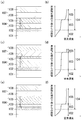
- FIG. 1A, FIG. 1C, and FIG. 1E are cross-sectional views of a semiconductor device according to an embodiment of the present invention, respectively, and FIG. 1B, FIG. 1 (f) is a graph showing nitrogen concentration profiles in the semiconductor devices shown in FIGS. 1 (a), 1 (c) and 1 (e), respectively.
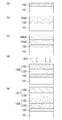
- 2A to 2E are cross-sectional views showing a method of manufacturing a semiconductor device according to an embodiment of the present invention in the order of steps.
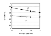
- FIG. 3 is a graph showing the relationship between the thickness of the HfSiO film and the O / Hf atomic ratio in the HfSiO film.
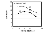
- FIG. 4 is a graph showing the relationship between the film thickness of the HfSiO film and the nitrogen concentration in the HfSiO film.
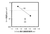
- FIG. 5 is a graph showing the relationship between the equivalent silicon oxide film thickness and the leakage current Jg.
- FIG. 1A, 1C, and 1E are cross-sectional views of a semiconductor device according to an embodiment of the present invention, respectively, and FIG. 1B, FIG. 1D, and FIG. (F) is a graph which shows the nitrogen concentration profile in the semiconductor device shown to Fig.1 (a), FIG.1 (c), and FIG.1 (e), respectively.
- an interfacial oxide layer 102 and gate insulation are formed on the upper surface of a semiconductor substrate 101 made of silicon or the like.
- a film 104 and a gate electrode 107 are provided in this order.
- the interface oxide layer 102 is a silicon oxide film or a silicon oxynitride film and has a thickness of 1.5 nm or less.
- the gate electrode 107 is composed of a metal gate electrode 106 and a polysilicon electrode 108.
- the metal gate electrode 106 is provided on the upper surface of the gate insulating film 104 and is made of, for example, TiN, TiAlN, TaC, or TaCN.
- the polysilicon electrode 108 is provided on the upper surface of the metal gate electrode 106 and contains impurities such as arsenic or boron.
- the gate insulating film 104 will be described in detail below.
- the gate insulating film 104 is composed of a first high dielectric film 103 and a second high dielectric film 105.
- the first high dielectric film 103 is provided on the upper surface of the interfacial oxide layer 102, and the HfO 2 film or the HfSiO film contains nitrogen.
- the second high dielectric film 105 is provided on the upper surface of the first high dielectric film 103, and the HfO 2 film or the HfSiO film contains nitrogen.
- the nitrogen concentration in the first high dielectric film 103 is lower than the nitrogen concentration in the second high dielectric film 105, and the difference is preferably 1 atomic% or more. Thereby, nitrogen can be prevented from diffusing from the gate insulating film 104 to the semiconductor substrate 101.
- the second high dielectric film (high dielectric film having a high nitrogen concentration) is in contact with the interface oxide layer. Therefore, in such a semiconductor device, since nitrogen diffuses from the gate insulating film to the interface between the interface oxide layer and the semiconductor substrate, there is a possibility that the semiconductor constituting the semiconductor substrate and nitrogen are combined. Therefore, the characteristics of the MOSFET are deteriorated.
- the gate insulating film is formed only of the first high dielectric film, it is possible to prevent nitrogen from diffusing into the semiconductor substrate.
- the heat treatment is performed after the gate insulating film is formed, there is a risk of causing crystallization of the HfSiO film, phase separation in the HfSiO film, penetration of impurities, and the like. In this case, it is difficult to compensate for oxygen vacancies or the like in the HfSiO film.
- the first high dielectric film 103 is provided between the interface oxide layer 102 and the second high dielectric film 105. That is, the first high dielectric film 103 is in contact with the interface oxide layer 102. Therefore, in the semiconductor device according to this embodiment, nitrogen can be prevented from diffusing from the gate insulating film 104 to the interface between the interfacial oxide layer 102 and the semiconductor substrate 101, so that the nitrogen (the main substrate) constituting the semiconductor substrate 101 In the embodiment, bonding with silicon) can be suppressed.
- the second high dielectric film 105 is provided on the upper surface of the first high dielectric film 103. Therefore, in the semiconductor device according to the present embodiment, even if the heat treatment is performed after the gate insulating film 104 is formed, the HfSiO film can be prevented from being crystallized in the gate insulating film 104, and the HfSiO film can be phased in the gate insulating film 104. Separation can be prevented and impurities can be prevented from penetrating into the semiconductor substrate 101. Further, in the gate insulating film 104, particularly in the second high dielectric film 105, oxygen vacancies or the like in the HfSiO film can be compensated.
- Nitrogen is uniformly distributed in the first high dielectric film 103 and is uniformly distributed in the second high dielectric film 105. Therefore, the nitrogen concentration rapidly changes at the interface between the first high dielectric film 103 and the second high dielectric film 105.
- the nitrogen concentration profile in the gate insulating film 104 can be changed by changing the ratio between the thickness of the first high dielectric film 103 and the thickness of the second high dielectric film 105.
- the ratio of the film thickness T 1 of the first high dielectric film 103 to the film thickness T 2 of the second high dielectric film 105 is 1, (T 1 ⁇ T 2 )
- the nitrogen concentration changes abruptly at the center in the film thickness direction of the gate insulating film 104 as shown in FIG.
- the occupation ratio of the first high dielectric film 103 in the gate insulating film 104 is higher than that shown in FIG. Accordingly, it is possible to suppress diffusion of nitrogen from the gate insulating film 104 to the interface between the interface oxide layer 102 and the semiconductor substrate 101 as compared with the case illustrated in FIG.
- the thickness T 1 is 1 of the first high dielectric film 103 with respect to the film thickness T 2 of the second high dielectric film 105 as shown in FIG. 1 (e) (T 1 ⁇ As shown in FIG. 1F, the T 2 ) and nitrogen concentration change abruptly at a position closer to the interface oxide layer 102 than the center in the film thickness direction of the gate insulating film 104.
- the first high dielectric film 103 may contain a metal (first metal) other than hafnium. For example, at least one of Al, La, Zr, Ti, Ta, Mg, Ge, and Y is used. It may contain one.
- the second high dielectric film 105 may contain a metal (second metal) other than hafnium. For example, at least one of Al, La, Zr, Ti, Ta, Mg, Ge, and Y may be contained. It may contain one.
- 2A to 2E are cross-sectional views showing the method of manufacturing the semiconductor device according to this embodiment in the order of steps.
- the upper surface of the semiconductor substrate 101 made of silicon or the like is cleaned using NH 4 OH, H 2 O 2 and H 2 O. Thereafter, a silicon oxide film or a silicon oxynitride film having a thickness of 1.5 nm or less is formed on the upper surface of the semiconductor substrate 101 by using, for example, a thermal oxidation method. Thereby, the interface oxide layer 102 is formed on the semiconductor substrate 101 (step (a)). At this time, a silicon oxide film or a silicon oxynitride film may be formed using O 2 , N 2 O, or NO gas at a processing temperature of 700 ° C. to 1000 ° C.
- step (b1) to form a first high-dielectric material film 103A made of HfO 2 film or HfSiO film on the upper surface of the interfacial oxide layer 102 (step (b1)).
- a second high dielectric material film 105A made of an HfO 2 film or an HfSiO film is formed on the upper surface of the first high dielectric material film 103A (step (b2)). )).
- the atomic ratio of O to Hf in the second high dielectric material film 105A is equal to or less than the atomic ratio of O to Hf in the first high dielectric material film 103A.
- the atomic ratio of O to Hf in the first high dielectric material film 103A is a and the atomic ratio of O to Hf in the second high dielectric material film 105A is b, b / a ⁇ 1 Meet.
- the surface of the second high-dielectric material film 105A is irradiated with nitrogen-containing plasma 201 when the temperature of the semiconductor substrate 101 is 20 to 150.degree.
- nitrogen is added to the first high dielectric material film 103A to form the first high dielectric material film 103
- nitrogen is added to the second high dielectric material film 105A to form the second high dielectric material film 103A.
- the body film 105 is formed, and the gate insulating film 104 made of the first high dielectric film 103 and the second high dielectric film 105 is formed (step (b3)).
- the nitrogen concentration in the first high dielectric material film 103 is the second high dielectric material film 103A. It becomes lower than the nitrogen concentration in the dielectric film 105.
- the nitrogen concentration in the second high dielectric film 105 is preferably 20 atomic% or less.
- high temperature heat treatment may be performed at a heat treatment temperature of 800 to 1100 ° C. in an oxygen atmosphere or a nitrogen atmosphere.
- a heat treatment temperature 800 to 1100 ° C. in an oxygen atmosphere or a nitrogen atmosphere.
- a TiN film, a TiAlN film, a TaC film, or a TaCN film is formed on the upper surface of the second high dielectric film 105.
- the metal gate electrode 106 is formed on the upper surface of the second high dielectric film 105.
- a silicon film containing a conductive impurity such as phosphorus, arsenic, or boron is formed on the upper surface of the metal gate electrode 106.
- a polysilicon electrode 108 is formed on the upper surface of the metal gate electrode 106, and a gate electrode 107 composed of the metal gate electrode 106 and the polysilicon electrode 108 is formed.
- first high dielectric film 103 and the second high dielectric film 105 will be described in detail.
- first, a method for manufacturing the first high dielectric material film 103A and the second high dielectric material film 105A will be described.
- the first high-dielectric material film 103A and the second high-dielectric material film 105A are preferably formed using an atomic layer deposition method. Specifically, when the first high dielectric material film 103A is an HfO 2 film, a step of supplying a first gas (hafnium-containing gas) to the upper surface of the interface oxide layer 102 for a first time. And the step of supplying the first oxidizing agent (including oxygen) for the second time on the upper surface of the interface oxide layer 102 may be alternately repeated.
- the first high dielectric material film 103A is an HfSiO film
- the first gas and the silicon gas may be supplied at the same time.
- the step of supplying the first gas and the first oxidizing agent The silicon gas may be supplied for a first time between the step of supplying the first time.
- the second high dielectric material film 105A is an HfO 2 film
- the second gas (hafnium-containing gas) is supplied to the upper surface of the first high dielectric material film 103A for the third time.
- the step of supplying the second oxidant (including oxygen) for a fourth time on the upper surface of the first high dielectric material film 103A may be alternately repeated.
- the second high dielectric material film 105A is an HfSiO film
- the second gas and the silicon gas may be supplied at the same time.
- the silicon gas may be supplied for a third time between the step of supplying the silicon gas.
- the second time is longer than the fourth time.
- the second time and the fourth time are times for supplying oxygen
- b / a ⁇ 1 can be obtained by setting the second time to be longer than the fourth time.
- the method of b / a ⁇ 1 is not limited to this method.
- the materials of the first gas and the second gas may be optimized and the materials of the first oxidant and the second oxidant may be optimized.
- first gas and the second gas examples include TDMA hafnium (TDMAHf (tetrakisdimethylaminohafnium), HfCl 4 (hafnium tetrachloride), TEMA hafnium (tetrakisethylmethylaminohafnium, tetrakis). at least one of (ethylmethylamino) hafnium) and hafnium (MMP) 4 [tetrakis (1-methoxy-2-methyl-2-propoxy) hafnium, (Tetrakis 1-Methoxy-2-methyl-2-propoxy hafnium)] It is preferable to select.
- TDMAHf tetrakisdimethylaminohafnium
- HfCl 4 hafnium tetrachloride
- TEMA hafnium tetrakisethylmethylaminohafnium, tetrakis.
- MMP hafnium
- the silicon gas includes at least one of 3DMAS (trisdimethylaminosilane), SiCl 4 (silicon tetrachloride) and Si (MMP) 4 [tetrakis (1-methoxy-2-methyl-2-propoxy) silicon]. It is preferable to select one.
- 3DMAS trisdimethylaminosilane
- SiCl 4 silicon tetrachloride
- Si (MMP) 4 tetrakis (1-methoxy-2-methyl-2-propoxy) silicon]. It is preferable to select one.
- the amount of nitrogen added to the first high dielectric material film 103A is different from each other.
- the smaller the atomic ratio of oxygen to hafnium in the high dielectric material film that is, the greater the amount of oxygen vacancies in the high dielectric material film
- the more the nitrogen-containing plasma is irradiated.
- An amount of nitrogen is added. Therefore, if the atomic ratio of oxygen to hafnium in the high dielectric material film is controlled, the amount of nitrogen added when the plasma containing nitrogen is irradiated can be controlled.
- a high dielectric material film having a large atomic ratio of oxygen to hafnium that is, the first high dielectric material film 103A
- a high dielectric material film having a small atomic ratio of oxygen to hafnium that is, the second high dielectric material film.
- the high dielectric material film 105A is formed as an upper layer
- the nitrogen concentration of the portion of the gate insulating film 104 located near the semiconductor substrate 101 is set to the nitrogen concentration of the portion of the gate insulating film 104 located near the gate electrode 107. It can be lower than the nitrogen concentration. Therefore, nitrogen can be prevented from diffusing from the gate insulating film 104 to the interface between the semiconductor substrate 101 and the interface oxide layer 102.
- first and second high dielectric films 103 and 105 contain nitrogen, the first and second high dielectric films 103 and 105 even if the semiconductor substrate 101 is subjected to a heat treatment in a later process. And the occurrence of phase separation in the first and second high dielectric films 103 and 105 can be suppressed.
- the amount of nitrogen added to the high dielectric material film can be changed by changing the atomic ratio of oxygen to hafnium in the high dielectric material film.
- the inventors of the present application have conceived the present invention by paying attention to a method for forming a high dielectric material film in order to control the atomic ratio of oxygen to hafnium in the high dielectric material film. The details will be described below.
- FIG. 3 is a graph showing the relationship between the film thickness of the HfSiO film and the atomic ratio of oxygen to hafnium in the HfSiO film, and is a result measured using EPMA (Electron Probe Micro Analyzer). Both the lines (a) and (b) in FIG. 3 are the results when the HfSiO film is formed by using the ALD method, and the material gas is different between the lines (a) and (b).
- the line (a) in FIG. 3 shows the results when the HfSiO film is formed using TDMA hafnium as the gas containing hafnium, 3DMAS as the silicon gas, and ozone as the oxidizing agent.
- a line (b) in FIG. 3 shows a result when an HfSiO film is formed using HfCl 4 as a gas containing hafnium, SiCl 4 as a silicon gas, and H 2 O as an oxidizing agent.
- an HfSiO film is formed using a gas containing carbon (3DMAS) as a silicon gas
- 3DMAS gas containing carbon
- a HfSiO film is formed using a gas containing chlorine as a silicon gas (SiCl 4 )
- SiCl 4 silicon gas
- about 3 atom% or less of chlorine may remain in the HfSiO film.
- the HfSiO film is formed using a gas containing chlorine as the silicon gas, defects are formed in the HfSiO film if chlorine is degassed during the deposition of the HfSiO film.
- the atomic radius of chlorine is larger than the atomic radius of nitrogen. For this reason, defects larger than nitrogen are formed in the HfSiO film, so that a large amount of nitrogen can be added to such an HfSiO film.
- the HfSiO film shown in the line (a) contains more oxygen than the HfSiO film shown in the line (b), that is, the HfSiO film shown in the line (a) is more line (b). It can be seen that there are fewer oxygen vacancies than the HfSiO film shown in FIG. Thus, by changing the material gas of the HfSiO film, the atomic ratio of oxygen to hafnium in the HfSiO film can be changed.
- FIG. 4 is a graph showing the relationship between the film thickness of the HfSiO film and the nitrogen concentration in the HfSiO film, and is a result measured by X-ray electron spectroscopy (X-ray photoelectron spectroscopy).
- Each of the lines (a) and (b) in FIG. 4 is a HfSiO obtained by performing heat treatment at 1000 ° C. or higher in a nitrogen atmosphere after irradiating the high dielectric material film with nitrogen-containing plasma. The relationship between the nitrogen concentration in the film and the film thickness is shown.
- the line (a) in FIG. 4 shows the result when the high dielectric material film shown in the line (a) in FIG. 3 is used as the high dielectric material film, and the line (b) in FIG. 4 shows the high dielectric material film. It is a result at the time of using the high dielectric material film
- the HfSiO film shown by the line (b) in FIG. 4 has 1 to 2 in the HfSiO film shown by the line (a) in FIG. Nitrogen as much as about atomic percent is added. From this result, it can be seen that many nitrogen atoms are added to an HfSiO film having a low atomic ratio of oxygen to hafnium, that is, an HfSiO film having a large amount of oxygen vacancies in the film.
- the inventors of the present invention have arranged the HfSiO film having a small amount of oxygen vacancies (the HfSiO film shown by line (a) in FIG. 3) at a position close to the semiconductor substrate 101, and the HfSiO film having a large amount of oxygen vacancies (FIG. 3). If the HfSiO film shown in line (b) of FIG. 5 is disposed at a position close to the gate electrode 107, an HfSiO film having a low nitrogen concentration can be formed at a position close to the semiconductor substrate 101. Found that an HfSiO film having a high nitrogen concentration can be formed.
- FIG. 5 is a graph showing the relationship between the equivalent thickness of silicon oxide film (EOT, equivalent oxide) and the leakage current Jg.
- the equivalent silicon oxide film thickness is a film thickness of the insulating film obtained by calculating back from the gate capacitance assuming that the material of the gate insulating film is silicon oxide.
- a point (A) in FIG. 5 shows a result when the semiconductor device according to the present embodiment is used.
- a gate electrode and a gate electrode made of a polysilicon electrode containing impurities such as phosphorus are sequentially provided.
- the first high dielectric film is formed by adding nitrogen to the first high dielectric material film formed using TDMA hafnium and ozone.
- the second high dielectric film is a film obtained by adding nitrogen to the second high dielectric material film formed using HfCl 4 and H 2 O.
- the film thickness ratio between the film thickness of the first high dielectric film and the film thickness of the second high dielectric film is 1: 1.
- the line (B) in FIG. 5 shows the result when only the HfSiO film formed using HfCl 4 and H 2 O is used as the gate insulating film.
- the leak current Jg is 0.7 A / cm 2 at the line (B) and 0.1 A / cm 2 at the point (A). From this, when the HfSiO film having a high nitrogen concentration formed on the upper surface of the HfSiO film having a low nitrogen concentration is used as the gate insulating film, compared with the case where only the HfSiO film having a high nitrogen concentration is used as the gate insulating film. Thus, it was found that the leakage current can be reduced to about 1/7.
- the gate insulating film 104 includes the first high dielectric film 103 and the second high dielectric film 105, and the nitrogen concentration in the first high dielectric film 103 is the second high dielectric film 103. It is lower than the nitrogen concentration in the dielectric film 105. Therefore, it is possible to prevent nitrogen from diffusing into the semiconductor substrate 101 as compared with the case where the gate insulating film is composed only of the second high dielectric film 105. Accordingly, it is possible to suppress nitrogen from being combined with a semiconductor included in the semiconductor substrate 101. Thereby, the characteristics of the semiconductor device can be improved. For example, as shown in FIG. 5, the leakage current can be greatly reduced.
- the thermal stability of the gate insulating film 104 can be improved as compared with the case where the gate insulating film is composed of only the first high dielectric film 103. Therefore, crystallization can be suppressed in each of the first high dielectric film 103 and the second high dielectric film 105, and the occurrence of phase separation can be suppressed.
- the present embodiment may have the following configuration.
- the semiconductor device preferably includes a sidewall, an extension region, a source / drain region, a silicide layer, and the like.
- a sidewall is preferably formed on the side surface of the gate electrode 107, and an extension region is preferably formed in the semiconductor substrate 101 below the side of the gate electrode 107.
- a source / drain region is preferably formed in the lower side of the side wall in 101, and a silicide layer is preferably formed on the upper surface of the gate electrode 107 and the upper surface of the source / drain region.
- the semiconductor device manufacturing method includes a step of forming a sidewall on the side surface of the gate electrode 107, a step of forming an extension region below the side of the gate electrode 107 in the semiconductor substrate 101, and a semiconductor
- the method further includes a step of forming a source / drain region below the side wall of the substrate 101 and a step of forming a silicide layer above the gate electrode 107 and above the source / drain region.
- the first and second high dielectric material films may be formed using metalorganic vapor phase deposition (metallorganic chemical vapor deposition).
- the semiconductor device and the method for manufacturing the semiconductor device according to the present invention are preferably used for various electronic devices using a semiconductor integrated circuit.
Abstract
Disclosed is a semiconductor device comprising an interfacial oxide layer (102), a gate insulating film (104) and a gate electrode (107), provided in that order upon the upper surface of a semiconductor substrate (101). The gate insulating film (104) comprises a first highly dielectric film (103) and a second highly dielectric film (105). The first highly dielectric film (103) is provided on the interfacial oxide layer (102), and contains nitrogen. The second highly dielectric film (105) is provided on the first highly dielectric film (103), and contains nitrogen. The nitrogen concentration in the first highly dielectric film (103) is lower than that in the second highly dielectric film (105).
Description
本発明は、半導体装置及びその製造方法に関し、詳細には高誘電体膜をゲート絶縁膜とする半導体装置及びその製造方法に関する。
The present invention relates to a semiconductor device and a manufacturing method thereof, and more particularly to a semiconductor device having a high dielectric film as a gate insulating film and a manufacturing method thereof.
MOSFET(metal oxide semiconductor field-effect transistor)の高速化に伴い、電界一定スケーリング則に従ってトランジスタの微細化が進行している。MOSFETの性能は、電流駆動能力Gmで表すことができ、キャリア移動度μ、ゲート幅W及びキャパシタ(ゲート電極、ゲート絶縁膜及びシリコン基板からなる)の静電容量Coxに比例し、ゲート長Lに反比例する。また、キャパシタの静電容量Coxは、Cox=ε0・ε・(S/d)(ε0:真空の誘電率、ε:ゲート絶縁膜の比誘電率、S:ゲート面積、d:ゲート絶縁膜の膜厚)で表される。よって、ゲート絶縁膜の膜厚dを薄くすれば、又は、ゲート長Lを短くすれば、MOSFETの性能を向上させることができる。従って、MOSFETの高性能化を実現させるために、シリコン酸化膜及びシリコン酸窒化膜等からなるゲート絶縁膜が薄膜化されており、ポリシリコン等からなるゲート電極のゲート長が短縮化されている。
As the speed of MOSFETs (metal oxide semiconductor field-effect transistors) increases, miniaturization of transistors progresses according to a constant electric field scaling rule. The performance of the MOSFET can be expressed by a current driving capability Gm, which is proportional to the carrier mobility μ, the gate width W, and the capacitance Cox of the capacitor (consisting of a gate electrode, a gate insulating film, and a silicon substrate), and a gate length L Inversely proportional to The capacitance Cox of the capacitor is Cox = ε 0 · ε · (S / d) (ε 0 : dielectric constant of vacuum, ε: relative dielectric constant of gate insulating film, S: gate area, d: gate insulation (Film thickness). Therefore, if the thickness d of the gate insulating film is reduced or the gate length L is shortened, the performance of the MOSFET can be improved. Therefore, in order to realize high performance of the MOSFET, the gate insulating film made of a silicon oxide film, a silicon oxynitride film or the like is thinned, and the gate length of the gate electrode made of polysilicon or the like is shortened. .
しかし、MOSFETの高性能化には、以下の様な課題がある。ゲート絶縁膜の膜厚を2nm以下まで薄くすると、直接トンネル電流が増加するので、ゲート電圧印加時におけるゲート絶縁膜の絶縁耐性が著しく劣化する。そのため、MOSFETの消費電力が増加する。このように、ゲート絶縁膜の膜厚を薄くすると、MOSFETの高性能化及び低消費電力化を図ることが難しい。
However, there are the following problems in improving the performance of MOSFETs. When the thickness of the gate insulating film is reduced to 2 nm or less, the tunnel current directly increases, so that the insulation resistance of the gate insulating film when the gate voltage is applied is significantly deteriorated. For this reason, the power consumption of the MOSFET increases. As described above, when the thickness of the gate insulating film is reduced, it is difficult to achieve high performance and low power consumption of the MOSFET.
ここで、上述のように、キャパシタの静電容量CoxはCox=ε0・ε・(S/d)で表される。よって、ゲート絶縁膜として従来のシリコン酸化膜(ε:3.9)及びシリコン酸窒化膜(ε:3.9~7)よりも比誘電率の大きな高誘電率ゲート絶縁膜(High-k膜)を用いれば、実効ゲート容量を維持しつつゲート絶縁膜の物理的膜厚を厚くすることができるので、直接トンネル電流を抑制することができる。
Here, as described above, the capacitance Cox of the capacitor is expressed by Cox = ε 0 · ε · (S / d). Therefore, a high dielectric constant gate insulating film (High-k film) having a relative dielectric constant larger than that of the conventional silicon oxide film (ε: 3.9) and silicon oxynitride film (ε: 3.9 to 7) is used as the gate insulating film. ), It is possible to increase the physical film thickness of the gate insulating film while maintaining the effective gate capacitance, so that the tunnel current can be directly suppressed.
High-k膜としては、ハフニウム酸化膜(HfO2膜)、ジリコニウム酸化膜(ZrO2膜)、アルミナ膜(Al2O3膜)及び希土類金属酸化物からなる膜等が注目されており、さらには、これらのシリケート膜及びアルミネート膜が注目されている。その中でも、HfO2膜及びHfSiO膜は、比誘電率が比較的高く、バンドギャップが5eV以上であり、シリコン基板との電子障壁高さが高いことから、次世代の高誘電率ゲート絶縁膜として最も有力である。
As the high-k film, a hafnium oxide film (HfO 2 film), a zirconium oxide film (ZrO 2 film), an alumina film (Al 2 O 3 film), a film made of a rare earth metal oxide, and the like have attracted attention. These silicate films and aluminate films are attracting attention. Among them, the HfO 2 film and the HfSiO film have a relatively high relative dielectric constant, a band gap of 5 eV or more, and a high electron barrier height with a silicon substrate. The most influential.
更に、MOSFETの微細化に伴い、ポリシリコンからなるゲート電極の空乏化を無視することができず、よって、ゲート容量の増加を図ることが難しい。そこで、ゲート電極として、ポリシリコン電極からメタル電極(空乏層による影響が無視できる)への置換が図られている。このように、次世代のゲート構造としては、High-k膜の上にメタル電極が形成された構造が有力である。
Furthermore, with the miniaturization of the MOSFET, depletion of the gate electrode made of polysilicon cannot be ignored, and therefore it is difficult to increase the gate capacitance. Therefore, replacement of a polysilicon electrode with a metal electrode (the influence of the depletion layer is negligible) is attempted as a gate electrode. Thus, as a next-generation gate structure, a structure in which a metal electrode is formed on a high-k film is prominent.
一般に、High-k膜は、低温で成膜される。そのため、HfO2膜及びHfSiO膜が成膜されると、酸素及び窒素雰囲気中において高温熱処理(PDA,PDAはpost-deposition annealの略語)が行われる。この高温熱処理により、High-k膜を緻密化させることができ、また、High-k膜における酸素欠損を補償することができる。
In general, the High-k film is formed at a low temperature. Therefore, when the HfO 2 film and the HfSiO film are formed, high-temperature heat treatment (PDA, PDA is an abbreviation for post-deposition anneal) is performed in an oxygen and nitrogen atmosphere. By this high-temperature heat treatment, the High-k film can be densified, and oxygen vacancies in the High-k film can be compensated.
しかし、この高温熱処理時に、High-k膜の結晶化又はHigh-k膜における相分離の発生などの問題が招来する。この問題は、ゲート電極に打ち込まれたボロン又はリンを活性化させるときに行う高速熱処理時においても、起こりうる。High-k膜の結晶化又はHigh-k膜における相分離が進行すると、High-k膜中に存在する結晶粒界を介してリーク電流が流れる虞があり、また、ゲート絶縁膜における比誘電率の不均一に起因してゲート絶縁膜の静電容量にばらつきが生じる。このような不具合を解消させる手段としてHigh-k膜に窒素を混入させるという手段が知られており、これにより、High-k膜の熱安定性を向上させることができる。
However, problems such as crystallization of the High-k film or occurrence of phase separation in the High-k film are caused during the high-temperature heat treatment. This problem can also occur during rapid heat treatment performed when activating boron or phosphorus implanted in the gate electrode. When crystallization of the High-k film or phase separation in the High-k film proceeds, a leakage current may flow through a crystal grain boundary existing in the High-k film, and a relative dielectric constant in the gate insulating film Due to the non-uniformity, the capacitance of the gate insulating film varies. As means for solving such a problem, means for mixing nitrogen into the High-k film is known, and thereby the thermal stability of the High-k film can be improved.
ところが、High-k膜の窒化時に、その窒素原子は、High-k膜内から半導体基板との界面まで到達し、半導体基板を構成する半導体(多くの場合シリコン)と結合する。このことは、半導体基板に対して熱処理を行った場合にも起こり得る。そのため、半導体基板とHigh-k膜との界面における欠陥密度の増大、High-k膜中に存在する固定電荷による閾値電圧の変動及びキャリア移動度の劣化等が招来する。つまり、MOSFETの特性劣化を招来する。
However, during nitriding of the High-k film, the nitrogen atoms reach from the inside of the High-k film to the interface with the semiconductor substrate, and are bonded to a semiconductor (in many cases, silicon) constituting the semiconductor substrate. This can also occur when a heat treatment is performed on the semiconductor substrate. For this reason, an increase in defect density at the interface between the semiconductor substrate and the High-k film, a change in threshold voltage due to a fixed charge existing in the High-k film, a deterioration in carrier mobility, and the like are caused. That is, the characteristics of the MOSFET are deteriorated.
本発明は、かかる点に鑑みてなされたものであり、その目的とするところは、ゲート絶縁膜としてHigh-k膜を用いた半導体装置及びその製造方法において、半導体装置の性能劣化を伴うことなく装置の微細化を図ることにある。
The present invention has been made in view of such a point, and an object of the present invention is to provide a semiconductor device using a high-k film as a gate insulating film and a method for manufacturing the same without causing deterioration in performance of the semiconductor device. The purpose is to miniaturize the apparatus.
本発明の半導体装置では、半導体基板の上面上に、界面酸化層、ゲート絶縁膜及びゲート電極が順に設けられている。ゲート絶縁膜は、界面酸化層の上に設けられた第1の高誘電体膜と、第1の高誘電体膜の上に設けられた第2の高誘電体膜とを有している。第1及び第2の高誘電体膜は窒素を含有しており、第1の高誘電体膜における窒素濃度は第2の高誘電体膜における窒素濃度よりも低い。
In the semiconductor device of the present invention, an interfacial oxide layer, a gate insulating film, and a gate electrode are sequentially provided on the upper surface of the semiconductor substrate. The gate insulating film has a first high dielectric film provided on the interface oxide layer and a second high dielectric film provided on the first high dielectric film. The first and second high dielectric films contain nitrogen, and the nitrogen concentration in the first high dielectric film is lower than the nitrogen concentration in the second high dielectric film.
このような半導体装置では、第1の高誘電体膜を備えていない半導体装置に比べて、窒素が半導体基板と界面酸化層との界面まで拡散することを防止できる。
In such a semiconductor device, it is possible to prevent nitrogen from diffusing up to the interface between the semiconductor substrate and the interface oxide layer, as compared with the semiconductor device not provided with the first high dielectric film.
また、このような半導体装置では、第2の高誘電体膜を備えていない半導体装置に比べて、熱処理時における高誘電体膜の結晶化及び相分離を抑制することができる。
Further, in such a semiconductor device, crystallization and phase separation of the high dielectric film during the heat treatment can be suppressed as compared with a semiconductor device that does not include the second high dielectric film.
本発明の半導体装置では、第1の高誘電体膜はハフニウムと酸素とを含有していることが好ましく、第2の高誘電体膜はハフニウムと酸素とを含有していることが好ましい。そして、第1の高誘電体膜におけるハフニウムに対する酸素の原子比をaとし第2の高誘電体膜におけるハフニウムに対する酸素の原子比をbとしたとき、b/a≦1であることが好ましい。これにより、比較的簡便な手法を用いて、第1の高誘電体膜における窒素濃度を第2の高誘電体膜における窒素濃度よりも低くすることができる。
In the semiconductor device of the present invention, the first high dielectric film preferably contains hafnium and oxygen, and the second high dielectric film preferably contains hafnium and oxygen. When the atomic ratio of oxygen to hafnium in the first high dielectric film is a and the atomic ratio of oxygen to hafnium in the second high dielectric film is b, it is preferable that b / a ≦ 1. Thereby, the nitrogen concentration in the first high dielectric film can be made lower than the nitrogen concentration in the second high dielectric film using a relatively simple technique.
後述の好ましい実施形態では、第1の高誘電体膜は、ハフニウムとは異なる第1の金属を含有している。第2の高誘電体膜は、ハフニウムとは異なる第2の金属を含有している。第1及び第2の金属は、Al、La、Zr、Ti、Ta、Mg、Ge及びYの少なくとも1つである。
In a preferred embodiment described later, the first high dielectric film contains a first metal different from hafnium. The second high dielectric film contains a second metal different from hafnium. The first and second metals are at least one of Al, La, Zr, Ti, Ta, Mg, Ge, and Y.
本発明の半導体装置の製造方法では、半導体基板の上面上に、界面酸化層、ゲート絶縁膜及びゲート電極を順に設ける。このとき、ゲート絶縁膜を設ける工程では、界面酸化層の上に第1及び第2の高誘電体材料膜を順に設けた後、第1の高誘電体材料膜に窒素を混入して第1の高誘電体膜を形成し、第2の高誘電体材料膜に窒素を混入して第1の高誘電体膜よりも窒素濃度が高い第2の高誘電体膜を形成する。
In the method for manufacturing a semiconductor device of the present invention, an interfacial oxide layer, a gate insulating film, and a gate electrode are sequentially provided on the upper surface of the semiconductor substrate. At this time, in the step of providing the gate insulating film, after the first and second high dielectric material films are sequentially provided on the interface oxide layer, nitrogen is mixed into the first high dielectric material film and the first high dielectric material film is mixed. The second high dielectric film is formed, and nitrogen is mixed into the second high dielectric material film to form a second high dielectric film having a higher nitrogen concentration than the first high dielectric film.
本発明の半導体装置の製造方法では、ハフニウムを含む第1のガスと酸素を含む第1の酸化剤とを用いて第1の高誘電体材料膜を形成することが好ましく、ハフニウムを含む第2のガスと酸素を含む第2の酸化剤とを用いて第2の高誘電体材料膜を形成することが好ましい。このとき、第1の高誘電体材料膜におけるハフニウムに対する酸素の原子比をaとし第2の高誘電体材料膜におけるハフニウムに対する酸素の原子比をbとしたときにb/a≦1となるように、第1の高誘電体材料膜及び第2の高誘電体材料膜を形成することが好ましい。これにより、第1の高誘電体材料膜における酸素濃度を第2の高誘電体材料膜における酸素濃度よりも高くすることができる。よって、第1の高誘電体材料膜に混入される窒素量を第2の高誘電体材料膜に混入される窒素量よりも少なくすることができる。
In the semiconductor device manufacturing method of the present invention, it is preferable to form the first high dielectric material film using the first gas containing hafnium and the first oxidizing agent containing oxygen, and the second gas containing hafnium. It is preferable to form the second high dielectric material film using the above gas and the second oxidizing agent containing oxygen. At this time, b / a ≦ 1 when the atomic ratio of oxygen to hafnium in the first high dielectric material film is a and the atomic ratio of oxygen to hafnium in the second high dielectric material film is b. In addition, it is preferable to form the first high dielectric material film and the second high dielectric material film. Thereby, the oxygen concentration in the first high dielectric material film can be made higher than the oxygen concentration in the second high dielectric material film. Therefore, the amount of nitrogen mixed in the first high dielectric material film can be made smaller than the amount of nitrogen mixed in the second high dielectric material film.
本発明の半導体装置の製造方法では、第1の高誘電体材料膜を形成する工程では、界面酸化層の上面上に第1のガスを第1の時間供給する工程と、界面酸化層の上面上に第1の酸化剤を第2の時間供給する工程とを繰り返し行えば良く、第2の高誘電体材料膜を形成する工程では、第1の高誘電体材料膜の上面上に第2のガスを第3の時間供給する工程と、第1の高誘電体材料膜の上面上に第2の酸化剤を第4の時間供給する工程とを繰り返し行えば良い。このとき、b/a≦1とするためには次に示す2つの方法のうちの何れか1つを選択すれば良い。1つ目の方法では、第1のガスを第2のガスと同一のガスとし、第1の酸化剤を第2の酸化剤と同一の酸化剤とし、第2の時間を第4の時間よりも長くする。2つ目の方法では、第1のガスとしてテトラキスジメチルアミノハフニウムを用い、第1の酸化剤としてオゾンを用い、第2のガスとしてテトラクロロハフニウムを用い、第2の酸化剤として水を用いる。
In the method for manufacturing a semiconductor device of the present invention, in the step of forming the first high dielectric material film, a step of supplying a first gas on the upper surface of the interface oxide layer for a first time, and an upper surface of the interface oxide layer The step of supplying the first oxidant for the second time may be repeated, and in the step of forming the second high dielectric material film, the second high dielectric material film is formed on the upper surface of the first high dielectric material film. The step of supplying the second gas for the third time and the step of supplying the second oxidant on the upper surface of the first high dielectric material film for the fourth time may be repeated. At this time, in order to satisfy b / a ≦ 1, one of the following two methods may be selected. In the first method, the first gas is the same gas as the second gas, the first oxidant is the same oxidant as the second oxidant, and the second time is greater than the fourth time. Also make it longer. In the second method, tetrakisdimethylaminohafnium is used as the first gas, ozone is used as the first oxidizing agent, tetrachlorohafnium is used as the second gas, and water is used as the second oxidizing agent.
本発明によれば、半導体装置の性能劣化を伴うことなく半導体装置の微細化を図ることができる。
According to the present invention, it is possible to miniaturize a semiconductor device without deteriorating the performance of the semiconductor device.
以下、本発明の実施形態に係る半導体製造装置及びその製造方法について、図面を参照しながら説明する。なお、本発明は、以下に示す実施形態に限定されない。
Hereinafter, a semiconductor manufacturing apparatus and a manufacturing method thereof according to an embodiment of the present invention will be described with reference to the drawings. In addition, this invention is not limited to embodiment shown below.
図1(a)、図1(c)及び図1(e)は、それぞれ、本発明の実施形態に係る半導体装置の断面図であり、図1(b)、図1(d)及び図1(f)は、それぞれ、図1(a)、図1(c)及び図1(e)に示す半導体装置における窒素濃度プロファイルを示すグラフ図である。
1A, 1C, and 1E are cross-sectional views of a semiconductor device according to an embodiment of the present invention, respectively, and FIG. 1B, FIG. 1D, and FIG. (F) is a graph which shows the nitrogen concentration profile in the semiconductor device shown to Fig.1 (a), FIG.1 (c), and FIG.1 (e), respectively.
図1(a)、図1(c)及び図1(e)に示すように、本実施形態に係る半導体装置では、シリコン等からなる半導体基板101の上面上に、界面酸化層102、ゲート絶縁膜104及びゲート電極107がこの順に設けられている。
As shown in FIGS. 1A, 1C, and 1E, in the semiconductor device according to the present embodiment, an interfacial oxide layer 102 and gate insulation are formed on the upper surface of a semiconductor substrate 101 made of silicon or the like. A film 104 and a gate electrode 107 are provided in this order.
界面酸化層102は、シリコン酸化膜又はシリコン酸窒化膜であり、1.5nm以下の膜厚を有している。ゲート電極107は、メタルゲート電極106とポリシリコン電極108とで構成されている。メタルゲート電極106は、ゲート絶縁膜104の上面上に設けられており、例えばTiN、TiAlN、TaC又はTaCNからなる。ポリシリコン電極108は、メタルゲート電極106の上面上に設けられており、ヒ素又はボロンなどの不純物を含んでいる。ゲート絶縁膜104について以下に詳述する。
The interface oxide layer 102 is a silicon oxide film or a silicon oxynitride film and has a thickness of 1.5 nm or less. The gate electrode 107 is composed of a metal gate electrode 106 and a polysilicon electrode 108. The metal gate electrode 106 is provided on the upper surface of the gate insulating film 104 and is made of, for example, TiN, TiAlN, TaC, or TaCN. The polysilicon electrode 108 is provided on the upper surface of the metal gate electrode 106 and contains impurities such as arsenic or boron. The gate insulating film 104 will be described in detail below.
ゲート絶縁膜104は、第1の高誘電体膜103と第2の高誘電体膜105とで構成されている。第1の高誘電体膜103は、界面酸化層102の上面上に設けられており、HfO2膜又はHfSiO膜に窒素が含有されたものである。第2の高誘電体膜105は、第1の高誘電体膜103の上面上に設けられており、HfO2膜又はHfSiO膜に窒素が含有されたものである。
The gate insulating film 104 is composed of a first high dielectric film 103 and a second high dielectric film 105. The first high dielectric film 103 is provided on the upper surface of the interfacial oxide layer 102, and the HfO 2 film or the HfSiO film contains nitrogen. The second high dielectric film 105 is provided on the upper surface of the first high dielectric film 103, and the HfO 2 film or the HfSiO film contains nitrogen.
第1の高誘電体膜103における窒素濃度は第2の高誘電体膜105における窒素濃度よりも低く、その差は1原子%以上であることが好ましい。これにより、窒素がゲート絶縁膜104から半導体基板101へ拡散することを防止できる。
The nitrogen concentration in the first high dielectric film 103 is lower than the nitrogen concentration in the second high dielectric film 105, and the difference is preferably 1 atomic% or more. Thereby, nitrogen can be prevented from diffusing from the gate insulating film 104 to the semiconductor substrate 101.
詳細には、ゲート絶縁膜が第2の高誘電体膜のみからなる場合、界面酸化層には第2の高誘電体膜(窒素濃度が高い高誘電体膜)が接することになる。そのため、このような半導体装置では、窒素がゲート絶縁膜から界面酸化層と半導体基板との界面まで拡散するので、半導体基板を構成する半導体と窒素とが結合する虞がある。よって、MOSFETの特性劣化を招来する。
Specifically, when the gate insulating film is composed of only the second high dielectric film, the second high dielectric film (high dielectric film having a high nitrogen concentration) is in contact with the interface oxide layer. Therefore, in such a semiconductor device, since nitrogen diffuses from the gate insulating film to the interface between the interface oxide layer and the semiconductor substrate, there is a possibility that the semiconductor constituting the semiconductor substrate and nitrogen are combined. Therefore, the characteristics of the MOSFET are deteriorated.
また、ゲート絶縁膜が第1の高誘電体膜のみからなる場合、窒素が半導体基板へ拡散することを防止できる。しかし、この場合、ゲート絶縁膜を形成した後に熱処理を行うと、HfSiO膜の結晶化、HfSiO膜における相分離及び不純物の突き抜け等を招来する虞がある。また、この場合、HfSiO膜中の酸素欠損等を補償することが難しい。
Further, when the gate insulating film is formed only of the first high dielectric film, it is possible to prevent nitrogen from diffusing into the semiconductor substrate. However, in this case, if the heat treatment is performed after the gate insulating film is formed, there is a risk of causing crystallization of the HfSiO film, phase separation in the HfSiO film, penetration of impurities, and the like. In this case, it is difficult to compensate for oxygen vacancies or the like in the HfSiO film.
一方、本実施形態では、第1の高誘電体膜103が界面酸化層102と第2の高誘電体膜105との間に設けられている。つまり、界面酸化層102には第1の高誘電体膜103が接することになる。よって、本実施形態に係る半導体装置では、窒素がゲート絶縁膜104から界面酸化層102と半導体基板101との界面まで拡散することを抑制できるので、その窒素が半導体基板101を構成する半導体(本実施形態ではシリコン)と結合することを抑制できる。従って、半導体基板101とゲート絶縁膜104との界面における欠陥密度の増大を防止することができ、第1の高誘電体膜103及び第2の高誘電体膜105中に存在する固定電荷による閾値電圧の変動を防止することができ、キャリア移動度の劣化等を防止することができる。つまり、MOSFETの特性劣化を防止することができる。
On the other hand, in the present embodiment, the first high dielectric film 103 is provided between the interface oxide layer 102 and the second high dielectric film 105. That is, the first high dielectric film 103 is in contact with the interface oxide layer 102. Therefore, in the semiconductor device according to this embodiment, nitrogen can be prevented from diffusing from the gate insulating film 104 to the interface between the interfacial oxide layer 102 and the semiconductor substrate 101, so that the nitrogen (the main substrate) constituting the semiconductor substrate 101 In the embodiment, bonding with silicon) can be suppressed. Accordingly, an increase in defect density at the interface between the semiconductor substrate 101 and the gate insulating film 104 can be prevented, and a threshold due to fixed charges existing in the first high dielectric film 103 and the second high dielectric film 105 can be prevented. Voltage fluctuation can be prevented, and deterioration of carrier mobility and the like can be prevented. That is, the characteristic deterioration of the MOSFET can be prevented.
また、本実施形態では、第2の高誘電体膜105が第1の高誘電体膜103の上面上に設けられている。よって、本実施形態に係る半導体装置では、ゲート絶縁膜104を形成した後に熱処理を行っても、ゲート絶縁膜104においてHfSiO膜が結晶化することを防止でき、ゲート絶縁膜104においてHfSiO膜が相分離を起こすことを防止でき、不純物が半導体基板101へ突き抜けることを防止できる。また、ゲート絶縁膜104では、特に第2の高誘電体膜105では、HfSiO膜中の酸素欠損等を補償することができる。
In the present embodiment, the second high dielectric film 105 is provided on the upper surface of the first high dielectric film 103. Therefore, in the semiconductor device according to the present embodiment, even if the heat treatment is performed after the gate insulating film 104 is formed, the HfSiO film can be prevented from being crystallized in the gate insulating film 104, and the HfSiO film can be phased in the gate insulating film 104. Separation can be prevented and impurities can be prevented from penetrating into the semiconductor substrate 101. Further, in the gate insulating film 104, particularly in the second high dielectric film 105, oxygen vacancies or the like in the HfSiO film can be compensated.
窒素は、第1の高誘電体膜103内において均一に分布しており、第2の高誘電体膜105内において均一に分布している。そのため、窒素濃度は、第1の高誘電体膜103と第2の高誘電体膜105との界面において急激に変化する。第1の高誘電体膜103の膜厚と第2の高誘電体膜105の膜厚との比を変更すれば、ゲート絶縁膜104における窒素濃度プロファイルを変更することができる。
Nitrogen is uniformly distributed in the first high dielectric film 103 and is uniformly distributed in the second high dielectric film 105. Therefore, the nitrogen concentration rapidly changes at the interface between the first high dielectric film 103 and the second high dielectric film 105. The nitrogen concentration profile in the gate insulating film 104 can be changed by changing the ratio between the thickness of the first high dielectric film 103 and the thickness of the second high dielectric film 105.
例えば、図1(a)に示すように第2の高誘電体膜105の膜厚T2に対する第1の高誘電体膜103の膜厚T1の比率が1であれば(T1≒T2)、窒素濃度は、図1(b)に示すように、ゲート絶縁膜104の膜厚方向における中央において急激に変化する。
For example, as shown in FIG. 1A, if the ratio of the film thickness T 1 of the first high dielectric film 103 to the film thickness T 2 of the second high dielectric film 105 is 1, (T 1 ≈T 2 ) The nitrogen concentration changes abruptly at the center in the film thickness direction of the gate insulating film 104 as shown in FIG.
また、図1(c)に示すように第2の高誘電体膜105の膜厚T2に対する第1の高誘電体膜103の膜厚T1の比率が1よりも大きければ(T1>T2)、窒素濃度は、図1(d)に示すように、ゲート絶縁膜104の膜厚方向における中央よりもゲート電極107に近い位置において急激に変化する。この場合、ゲート絶縁膜104における第1の高誘電体膜103の占有率は、図1(a)に示す場合よりも高い。よって、図1(a)に示す場合に比べて、窒素がゲート絶縁膜104から界面酸化層102と半導体基板101との界面まで拡散することを抑制することができる。
Further, if is greater than 1 the ratio of the thickness T 1 of the first high dielectric film 103 with respect to the film thickness T 2 of the second high dielectric film 105 as shown in FIG. 1 (c) (T 1> T 2 ) and the nitrogen concentration change rapidly at a position closer to the gate electrode 107 than the center in the film thickness direction of the gate insulating film 104 as shown in FIG. In this case, the occupation ratio of the first high dielectric film 103 in the gate insulating film 104 is higher than that shown in FIG. Accordingly, it is possible to suppress diffusion of nitrogen from the gate insulating film 104 to the interface between the interface oxide layer 102 and the semiconductor substrate 101 as compared with the case illustrated in FIG.
また、図1(e)に示すように第2の高誘電体膜105の膜厚T2に対する第1の高誘電体膜103の膜厚T1の割合が1よりも小さければ(T1<T2)、窒素濃度は、図1(f)に示すように、ゲート絶縁膜104の膜厚方向における中央よりも界面酸化層102に近い位置において急激に変化する。
Also, smaller than the proportion of the thickness T 1 is 1 of the first high dielectric film 103 with respect to the film thickness T 2 of the second high dielectric film 105 as shown in FIG. 1 (e) (T 1 < As shown in FIG. 1F, the T 2 ) and nitrogen concentration change abruptly at a position closer to the interface oxide layer 102 than the center in the film thickness direction of the gate insulating film 104.
なお、第1の高誘電体膜103は、ハフニウム以外の金属(第1の金属)を含有していても良く、例えば、Al、La、Zr、Ti、Ta、Mg、Ge及びYの少なくとも一つを含んでいても良い。また、第2の高誘電体膜105は、ハフニウム以外の金属(第2の金属)を含有していても良く、例えば、Al、La、Zr、Ti、Ta、Mg、Ge及びYの少なくとも一つを含んでいても良い。
The first high dielectric film 103 may contain a metal (first metal) other than hafnium. For example, at least one of Al, La, Zr, Ti, Ta, Mg, Ge, and Y is used. It may contain one. The second high dielectric film 105 may contain a metal (second metal) other than hafnium. For example, at least one of Al, La, Zr, Ti, Ta, Mg, Ge, and Y may be contained. It may contain one.
以下では、図2(a)~(e)を参照しながら、本実施形態に係る半導体装置の製造方法を説明する。図2(a)~(e)は、本実施形態に係る半導体装置の製造方法を工程順に示す断面図である。
Hereinafter, a method for manufacturing a semiconductor device according to the present embodiment will be described with reference to FIGS. 2 (a) to 2 (e). 2A to 2E are cross-sectional views showing the method of manufacturing the semiconductor device according to this embodiment in the order of steps.
まず、図2(a)に示す工程では、NH4OH、H2O2及びH2Oを用いて、シリコン等からなる半導体基板101の上面を洗浄する。その後、例えば熱酸化法を用いて、半導体基板101の上面上に、膜厚が1.5nm以下のシリコン酸化膜又はシリコン酸窒化膜を形成する。これにより、半導体基板101の上に界面酸化層102が形成される(工程(a))。このとき、O2、N2O又はNOガスを用い、且つ、処理温度を700℃~1000℃として、シリコン酸化膜又はシリコン酸窒化膜を形成すれば良い。
First, in the step shown in FIG. 2A, the upper surface of the semiconductor substrate 101 made of silicon or the like is cleaned using NH 4 OH, H 2 O 2 and H 2 O. Thereafter, a silicon oxide film or a silicon oxynitride film having a thickness of 1.5 nm or less is formed on the upper surface of the semiconductor substrate 101 by using, for example, a thermal oxidation method. Thereby, the interface oxide layer 102 is formed on the semiconductor substrate 101 (step (a)). At this time, a silicon oxide film or a silicon oxynitride film may be formed using O 2 , N 2 O, or NO gas at a processing temperature of 700 ° C. to 1000 ° C.
次に、図2(b)に示す工程では、界面酸化層102の上面上にHfO2膜又はHfSiO膜からなる第1の高誘電体材料膜103Aを形成する(工程(b1))。
Next, in a step shown in FIG. 2 (b), to form a first high-dielectric material film 103A made of HfO 2 film or HfSiO film on the upper surface of the interfacial oxide layer 102 (step (b1)).
続いて、図2(c)に示す工程では、第1の高誘電体材料膜103Aの上面上にHfO2膜又はHfSiO膜からなる第2の高誘電体材料膜105Aを形成する(工程(b2))。このとき、第2の高誘電体材料膜105AにおけるHfに対するOの原子比は、第1の高誘電体材料膜103AにおけるHfに対するOの原子比以下である。好ましくは、第1の高誘電体材料膜103AにおけるHfに対するOの原子比をaとし、第2の高誘電体材料膜105AにおけるHfに対するOの原子比をbとしたとき、b/a≦1を満たしている。
2C, a second high dielectric material film 105A made of an HfO 2 film or an HfSiO film is formed on the upper surface of the first high dielectric material film 103A (step (b2)). )). At this time, the atomic ratio of O to Hf in the second high dielectric material film 105A is equal to or less than the atomic ratio of O to Hf in the first high dielectric material film 103A. Preferably, when the atomic ratio of O to Hf in the first high dielectric material film 103A is a and the atomic ratio of O to Hf in the second high dielectric material film 105A is b, b / a ≦ 1 Meet.
続いて、図2(d)に示す工程では、半導体基板101の温度が20~150℃下において、窒素を含有するプラズマ201を第2の高誘電体材料膜105Aの表面に照射する。これにより、第1の高誘電体材料膜103Aに窒素が添加されて第1の高誘電体膜103が形成され、第2の高誘電体材料膜105Aに窒素が添加されて第2の高誘電体膜105が形成され、第1の高誘電体膜103及び第2の高誘電体膜105からなるゲート絶縁膜104が形成される(工程(b3))。このとき、第1の高誘電体材料膜103Aには第2の高誘電体材料膜105Aよりも少量の窒素が添加されるので、第1の高誘電体膜103における窒素濃度は第2の高誘電体膜105における窒素濃度よりも低くなる。第2の高誘電体膜105中の窒素濃度は、20原子%以下であることが好ましい。
2D, the surface of the second high-dielectric material film 105A is irradiated with nitrogen-containing plasma 201 when the temperature of the semiconductor substrate 101 is 20 to 150.degree. Thus, nitrogen is added to the first high dielectric material film 103A to form the first high dielectric material film 103, and nitrogen is added to the second high dielectric material film 105A to form the second high dielectric material film 103A. The body film 105 is formed, and the gate insulating film 104 made of the first high dielectric film 103 and the second high dielectric film 105 is formed (step (b3)). At this time, since a smaller amount of nitrogen is added to the first high dielectric material film 103A than the second high dielectric material film 105A, the nitrogen concentration in the first high dielectric material film 103 is the second high dielectric material film 103A. It becomes lower than the nitrogen concentration in the dielectric film 105. The nitrogen concentration in the second high dielectric film 105 is preferably 20 atomic% or less.
その後、酸素雰囲気中又は窒素雰囲気中において、熱処理温度を800~1100℃とする高温熱処理を行っても良い。これにより、第1及び第2の高誘電体膜103,105の緻密化を図ることができ、第1及び第2の高誘電体膜103,105からの窒素抜けを防止することができる。
Thereafter, high temperature heat treatment may be performed at a heat treatment temperature of 800 to 1100 ° C. in an oxygen atmosphere or a nitrogen atmosphere. As a result, the first and second high dielectric films 103 and 105 can be densified, and nitrogen desorption from the first and second high dielectric films 103 and 105 can be prevented.
それから、図2(e)に示す工程では、第2の高誘電体膜105の上面上にTiN膜、TiAlN膜、TaC膜又はTaCN膜を形成する。これにより、第2の高誘電体膜105の上面上にメタルゲート電極106が形成される。その後、メタルゲート電極106の上面上にリン、ヒ素又はボロン等の導電性を有する不純物を含んだシリコン膜を形成する。これにより、メタルゲート電極106の上面上にポリシリコン電極108が形成され、メタルゲート電極106及びポリシリコン電極108からなるゲート電極107が形成される。
Then, in the step shown in FIG. 2E, a TiN film, a TiAlN film, a TaC film, or a TaCN film is formed on the upper surface of the second high dielectric film 105. As a result, the metal gate electrode 106 is formed on the upper surface of the second high dielectric film 105. After that, a silicon film containing a conductive impurity such as phosphorus, arsenic, or boron is formed on the upper surface of the metal gate electrode 106. As a result, a polysilicon electrode 108 is formed on the upper surface of the metal gate electrode 106, and a gate electrode 107 composed of the metal gate electrode 106 and the polysilicon electrode 108 is formed.
以下では、第1の高誘電体膜103及び第2の高誘電体膜105の成膜方法を詳細に説明する。まず、第1の高誘電体材料膜103A及び第2の高誘電体材料膜105Aの製造方法を説明する。
Hereinafter, a method for forming the first high dielectric film 103 and the second high dielectric film 105 will be described in detail. First, a method for manufacturing the first high dielectric material film 103A and the second high dielectric material film 105A will be described.
第1の高誘電体材料膜103A及び第2の高誘電体材料膜105Aは、原子層蒸着(Atomic Layer Deposition)法を用いて作製されることが好ましい。具体的には、第1の高誘電体材料膜103AがHfO2膜である場合には、界面酸化層102の上面上に第1のガス(ハフニウムを含むガス)を第1の時間供給する工程と界面酸化層102の上面上に第1の酸化剤(酸素を含む)を第2の時間供給する工程とを交互に繰り返せば良い。また、第1の高誘電体材料膜103AがHfSiO膜である場合には、第1のガスとシリコンガスとを同時に供給しても良く、第1のガスを供給する工程と第1の酸化剤を供給する工程との間にシリコンガスを第1の時間供給しても良い。
The first high-dielectric material film 103A and the second high-dielectric material film 105A are preferably formed using an atomic layer deposition method. Specifically, when the first high dielectric material film 103A is an HfO 2 film, a step of supplying a first gas (hafnium-containing gas) to the upper surface of the interface oxide layer 102 for a first time. And the step of supplying the first oxidizing agent (including oxygen) for the second time on the upper surface of the interface oxide layer 102 may be alternately repeated. When the first high dielectric material film 103A is an HfSiO film, the first gas and the silicon gas may be supplied at the same time. The step of supplying the first gas and the first oxidizing agent The silicon gas may be supplied for a first time between the step of supplying the first time.
同じく、第2の高誘電体材料膜105AがHfO2膜である場合には、第1の高誘電体材料膜103Aの上面上に第2のガス(ハフニウムを含むガス)を第3の時間供給する工程と第1の高誘電体材料膜103Aの上面上に第2の酸化剤(酸素を含む)を第4の時間供給する工程とを交互に繰り返せば良い。また、第2の高誘電体材料膜105AがHfSiO膜である場合には、第2のガスとシリコンガスとを同時に供給しても良く、第2のガスを供給する工程と第2の酸化剤を供給する工程との間にシリコンガスを第3の時間供給しても良い。ここで、第1のガスと第2のガスとが同じであり、且つ、第1の酸化剤と第2の酸化剤とが同じである場合、第2の時間を第4の時間よりも長くすれば良い。第2の時間及び第4の時間は酸素を供給する時間であるので、第2の時間を第4の時間よりも長くすればb/a≦1とすることができる。なお、b/a≦1とする方法はこの方法に限定されない。後述のように、第1のガス及び第2のガスのそれぞれの材料を最適化するとともに第1の酸化剤及び第2の酸化剤のそれぞれの材料を最適化しても良い。
Similarly, when the second high dielectric material film 105A is an HfO 2 film, the second gas (hafnium-containing gas) is supplied to the upper surface of the first high dielectric material film 103A for the third time. And the step of supplying the second oxidant (including oxygen) for a fourth time on the upper surface of the first high dielectric material film 103A may be alternately repeated. When the second high dielectric material film 105A is an HfSiO film, the second gas and the silicon gas may be supplied at the same time. The step of supplying the second gas and the second oxidizing agent The silicon gas may be supplied for a third time between the step of supplying the silicon gas. Here, when the first gas and the second gas are the same, and the first oxidant and the second oxidant are the same, the second time is longer than the fourth time. Just do it. Since the second time and the fourth time are times for supplying oxygen, b / a ≦ 1 can be obtained by setting the second time to be longer than the fourth time. Note that the method of b / a ≦ 1 is not limited to this method. As will be described later, the materials of the first gas and the second gas may be optimized and the materials of the first oxidant and the second oxidant may be optimized.
第1のガス及び第2のガスとしては、例えば、TDMAハフニウム(TDMAHf(テトラキスジメチルアミノハフニウム,tetrakis(dimethylamino)hafnium))、HfCl4(四塩化ハフニウム)、TEMAハフニウム(テトラキスエチルメチルアミノハフニウム,tetrakis(ethylmethylamino)hafnium)及びハフニウム(MMP)4〔テトラキス(1-メトキシ-2-メチル-2-プロポキシ)ハフニウム,(Tetrakis 1-Methoxy-2-methyl-2-propoxy hafnium〕のうちの少なくとも一つを選択することが好ましい。
Examples of the first gas and the second gas include TDMA hafnium (TDMAHf (tetrakisdimethylaminohafnium), HfCl 4 (hafnium tetrachloride), TEMA hafnium (tetrakisethylmethylaminohafnium, tetrakis). at least one of (ethylmethylamino) hafnium) and hafnium (MMP) 4 [tetrakis (1-methoxy-2-methyl-2-propoxy) hafnium, (Tetrakis 1-Methoxy-2-methyl-2-propoxy hafnium)] It is preferable to select.
第1の酸化剤及び第2の酸化剤としては、O3(オゾン)及びH2O(水)の少なくとも一つを選択することが好ましい。
It is preferable to select at least one of O 3 (ozone) and H 2 O (water) as the first oxidant and the second oxidant.
シリコンガスとしては、3DMAS(トリスジメチルアミノシラン,trisdimethyl amino silane)、SiCl4(四塩化ケイ素)及びSi(MMP)4〔テトラキス(1-メトキシ-2-メチル-2-プロポキシ)シリコン〕のうちの少なくとも一つを選択することが好ましい。
The silicon gas includes at least one of 3DMAS (trisdimethylaminosilane), SiCl 4 (silicon tetrachloride) and Si (MMP) 4 [tetrakis (1-methoxy-2-methyl-2-propoxy) silicon]. It is preferable to select one.
本実施形態では、第1の高誘電体材料膜103Aと第2の高誘電体材料膜105Aとにおいて酸素濃度が互いに異なるので、第1の高誘電体材料膜103Aに添加される窒素の量と第2の高誘電体材料膜105Aに添加される窒素の量とが互いに異なる。具体的には、高誘電体材料膜中におけるハフニウムに対する酸素の原子比が小さいほど(つまり、高誘電体材料膜中における酸素欠損量が大きいほど)、窒素を含有するプラズマを照射したときには多くの窒素の量が添加される。よって、高誘電体材料膜中におけるハフニウムに対する酸素の原子比を制御すれば、窒素を含有するプラズマを照射したときに添加される窒素の量を制御することができる。従って、ハフニウムに対する酸素の原子比が大きい高誘電体材料膜(つまり第1の高誘電体材料膜103A)を下層に形成し、ハフニウムに対する酸素の原子比が小さい高誘電体材料膜(つまり第2の高誘電体材料膜105A)を上層に形成すれば、ゲート絶縁膜104のうち半導体基板101の近くに位置する部分の窒素濃度をゲート絶縁膜104のうちゲート電極107の近くに位置する部分の窒素濃度よりも低くすることができる。よって、窒素がゲート絶縁膜104から半導体基板101と界面酸化層102との界面まで拡散することを防止できる。また、第1及び第2の高誘電体膜103,105が窒素を含有しているので、後の工程において半導体基板101に熱処理を施しても第1及び第2の高誘電体膜103,105の結晶化を抑制できるとともに第1及び第2の高誘電体膜103,105における相分離の発生を抑制できる。
In the present embodiment, since the oxygen concentrations of the first high dielectric material film 103A and the second high dielectric material film 105A are different from each other, the amount of nitrogen added to the first high dielectric material film 103A The amount of nitrogen added to the second high dielectric material film 105A is different from each other. Specifically, the smaller the atomic ratio of oxygen to hafnium in the high dielectric material film (that is, the greater the amount of oxygen vacancies in the high dielectric material film), the more the nitrogen-containing plasma is irradiated. An amount of nitrogen is added. Therefore, if the atomic ratio of oxygen to hafnium in the high dielectric material film is controlled, the amount of nitrogen added when the plasma containing nitrogen is irradiated can be controlled. Therefore, a high dielectric material film having a large atomic ratio of oxygen to hafnium (that is, the first high dielectric material film 103A) is formed in the lower layer, and a high dielectric material film having a small atomic ratio of oxygen to hafnium (that is, the second high dielectric material film). If the high dielectric material film 105A) is formed as an upper layer, the nitrogen concentration of the portion of the gate insulating film 104 located near the semiconductor substrate 101 is set to the nitrogen concentration of the portion of the gate insulating film 104 located near the gate electrode 107. It can be lower than the nitrogen concentration. Therefore, nitrogen can be prevented from diffusing from the gate insulating film 104 to the interface between the semiconductor substrate 101 and the interface oxide layer 102. In addition, since the first and second high dielectric films 103 and 105 contain nitrogen, the first and second high dielectric films 103 and 105 even if the semiconductor substrate 101 is subjected to a heat treatment in a later process. And the occurrence of phase separation in the first and second high dielectric films 103 and 105 can be suppressed.
従来、高誘電体材料膜中のハフニウムに対する酸素の原子比を変更すれば高誘電体材料膜中への窒素の添加量を変更することができるということは、知られていなかった。本願発明者らは、高誘電体材料膜中のハフニウムに対する酸素の原子比を制御するために高誘電体材料膜の成膜方法に着目して、本願発明を想到した。以下、その詳細について説明する。
Conventionally, it has not been known that the amount of nitrogen added to the high dielectric material film can be changed by changing the atomic ratio of oxygen to hafnium in the high dielectric material film. The inventors of the present application have conceived the present invention by paying attention to a method for forming a high dielectric material film in order to control the atomic ratio of oxygen to hafnium in the high dielectric material film. The details will be described below.
図3は、HfSiO膜の膜厚とHfSiO膜中におけるハフニウムに対する酸素の原子比との関係を示すグラフ図であり、EPMA(Electron Probe Micro Analyzer)を用いて測定された結果である。図3中の線(a)及び線(b)はどちらもALD法を用いてHfSiO膜を作製した場合の結果であり、線(a)と線(b)とでは材料ガスが互いに異なる。
FIG. 3 is a graph showing the relationship between the film thickness of the HfSiO film and the atomic ratio of oxygen to hafnium in the HfSiO film, and is a result measured using EPMA (Electron Probe Micro Analyzer). Both the lines (a) and (b) in FIG. 3 are the results when the HfSiO film is formed by using the ALD method, and the material gas is different between the lines (a) and (b).
具体的には、図3中の線(a)は、ハフニウムを含むガスとしてTDMAハフニウムを用い、シリコンガスとして3DMASを用い、酸化剤としてオゾンを用いてHfSiO膜を作製した場合の結果である。図3中の線(b)は、ハフニウムを含むガスとしてHfCl4を用い、シリコンガスとしてSiCl4を用い、酸化剤としてH2Oを用いてHfSiO膜を作製した場合の結果である。
Specifically, the line (a) in FIG. 3 shows the results when the HfSiO film is formed using TDMA hafnium as the gas containing hafnium, 3DMAS as the silicon gas, and ozone as the oxidizing agent. A line (b) in FIG. 3 shows a result when an HfSiO film is formed using HfCl 4 as a gas containing hafnium, SiCl 4 as a silicon gas, and H 2 O as an oxidizing agent.
なお、シリコンガスとして炭素を含むガス(3DMAS)を用いてHfSiO膜を形成すると、そのHfSiO膜中には3原子%以下程度の炭素が残留する場合がある。また、シリコンガスとして塩素を含むガス(SiCl4)を用いてHfSiO膜を形成すると、そのHfSiO膜中には3原子%以下程度の塩素が残留する場合がある。シリコンガスとして塩素を含むガスを用いてHfSiO膜を形成するとき、そのHfSiO膜の堆積時に塩素の脱ガス化を行えば、HfSiO膜中には欠陥が形成される。ここで、塩素の原子半径は、窒素の原子半径よりも大きい。そのため、HfSiO膜中には窒素よりも大きな欠陥が形成されることになるので、このようなHfSiO膜には多くの窒素を添加することができる。
Note that when an HfSiO film is formed using a gas containing carbon (3DMAS) as a silicon gas, about 3 atomic% or less of carbon may remain in the HfSiO film. Further, when a HfSiO film is formed using a gas containing chlorine as a silicon gas (SiCl 4 ), about 3 atom% or less of chlorine may remain in the HfSiO film. When the HfSiO film is formed using a gas containing chlorine as the silicon gas, defects are formed in the HfSiO film if chlorine is degassed during the deposition of the HfSiO film. Here, the atomic radius of chlorine is larger than the atomic radius of nitrogen. For this reason, defects larger than nitrogen are formed in the HfSiO film, so that a large amount of nitrogen can be added to such an HfSiO film.
図3に示す線(a)及び線(b)を比較すると、ハフニウムを含むガスとしてTDMAハフニウムを用い酸化剤としてオゾンを用いてHfSiO膜を作製した場合(線(a))、HfSiO膜中におけるハフニウムに対する酸素の原子比は5.5~6程度である。一方、ハフニウムを含むガスとして4塩化ハフニウムを用い酸化剤として水を用いてHfSiO膜を作製した場合(線(b))、HfSiO膜中におけるハフニウムに対する酸素の原子比が4.5~5程度である。これにより、線(a)に示すHfSiO膜の方が線(b)に示すHfSiO膜よりも多くの酸素を含有している、つまり、線(a)に示すHfSiO膜の方が線(b)に示すHfSiO膜よりも酸素欠損が少ない、ということが分かる。このようにHfSiO膜の材料ガスを変更すれば、HfSiO膜中におけるハフニウムに対する酸素の原子比を変更することができる。
When the lines (a) and (b) shown in FIG. 3 are compared, when the HfSiO film is formed using TDMA hafnium as the gas containing hafnium and ozone as the oxidizing agent (line (a)), The atomic ratio of oxygen to hafnium is about 5.5-6. On the other hand, when an HfSiO film is formed using hafnium tetrachloride as the gas containing hafnium and water as the oxidizing agent (line (b)), the atomic ratio of oxygen to hafnium in the HfSiO film is about 4.5 to 5. is there. Thereby, the HfSiO film shown in the line (a) contains more oxygen than the HfSiO film shown in the line (b), that is, the HfSiO film shown in the line (a) is more line (b). It can be seen that there are fewer oxygen vacancies than the HfSiO film shown in FIG. Thus, by changing the material gas of the HfSiO film, the atomic ratio of oxygen to hafnium in the HfSiO film can be changed.
図4は、HfSiO膜の膜厚とHfSiO膜中における窒素濃度との関係を示すグラフ図であり、X線電子分光法(X-ray photoelectron spectroscopy)により測定された結果である。図4中の線(a)及び線(b)には何れも、窒素を含有するプラズマを高誘電体材料膜に照射した後に窒素雰囲気中において1000℃以上で熱処理を行うことにより得られたHfSiO膜中の窒素濃度とその膜厚との関係を示している。図4中の線(a)は高誘電体材料膜として図3中の線(a)に示す高誘電体材料膜を使用した場合の結果であり、図4中の線(b)は高誘電体材料膜として図3中の線(b)に示す高誘電体材料膜を使用した場合の結果である。
FIG. 4 is a graph showing the relationship between the film thickness of the HfSiO film and the nitrogen concentration in the HfSiO film, and is a result measured by X-ray electron spectroscopy (X-ray photoelectron spectroscopy). Each of the lines (a) and (b) in FIG. 4 is a HfSiO obtained by performing heat treatment at 1000 ° C. or higher in a nitrogen atmosphere after irradiating the high dielectric material film with nitrogen-containing plasma. The relationship between the nitrogen concentration in the film and the film thickness is shown. The line (a) in FIG. 4 shows the result when the high dielectric material film shown in the line (a) in FIG. 3 is used as the high dielectric material film, and the line (b) in FIG. 4 shows the high dielectric material film. It is a result at the time of using the high dielectric material film | membrane shown by the line (b) in FIG. 3 as a body material film | membrane.
図4に示す線(a)及び線(b)を比較すると、図4中の線(b)に示すHfSiO膜中には図4中の線(a)に示すHfSiO膜中よりも1~2原子%程度多くの窒素が添加されている。この結果から、ハフニウムに対する酸素の原子比が低いHfSiO膜、つまり、膜中の酸素欠損量が多いHfSiO膜には多くの窒素原子が添加されるということが分かる。
When the lines (a) and (b) shown in FIG. 4 are compared, the HfSiO film shown by the line (b) in FIG. 4 has 1 to 2 in the HfSiO film shown by the line (a) in FIG. Nitrogen as much as about atomic percent is added. From this result, it can be seen that many nitrogen atoms are added to an HfSiO film having a low atomic ratio of oxygen to hafnium, that is, an HfSiO film having a large amount of oxygen vacancies in the film.
以上より、本願発明者らは、酸素欠損量が少ないHfSiO膜(図3の線(a)に示すHfSiO膜)を半導体基板101に近い位置に配置し、酸素欠損量が多いHfSiO膜(図3の線(b)に示すHfSiO膜)をゲート電極107に近い位置に配置すれば、半導体基板101に近い位置には窒素濃度が低いHfSiO膜を形成することができ、ゲート電極107に近い位置には窒素濃度が高いHfSiO膜を形成することができるということを見出した。
As described above, the inventors of the present invention have arranged the HfSiO film having a small amount of oxygen vacancies (the HfSiO film shown by line (a) in FIG. 3) at a position close to the semiconductor substrate 101, and the HfSiO film having a large amount of oxygen vacancies (FIG. 3). If the HfSiO film shown in line (b) of FIG. 5 is disposed at a position close to the gate electrode 107, an HfSiO film having a low nitrogen concentration can be formed at a position close to the semiconductor substrate 101. Found that an HfSiO film having a high nitrogen concentration can be formed.
図5は、シリコン酸化膜換算膜厚(EOT,equivalent oxide thickness)とリーク電流Jgとの関係を示すグラフ図である。シリコン酸化膜換算膜厚とは、ゲート絶縁膜の材料がシリコン酸化物であると仮定してゲート容量から逆算して得られる絶縁膜の膜厚のことである。
FIG. 5 is a graph showing the relationship between the equivalent thickness of silicon oxide film (EOT, equivalent oxide) and the leakage current Jg. The equivalent silicon oxide film thickness is a film thickness of the insulating film obtained by calculating back from the gate capacitance assuming that the material of the gate insulating film is silicon oxide.
図5中の点(A)には、本実施形態に係る半導体装置を用いた場合の結果を示している。具体的には、シリコンからなる半導体基板の上面上に、1.5nm以下の膜厚を有するシリコン酸化膜と、第1及び第2の高誘電体膜からなるゲート絶縁膜と、TiNからなるメタルゲート電極及びリン等の不純物を含有するポリシリコン電極からなるゲート電極とが順に設けられている。ここで、第1の高誘電体膜は、TDMAハフニウム及びオゾンを用いて形成された第1の高誘電体材料膜に窒素が添加されたものである。第2の高誘電体膜は、HfCl4及びH2Oを用いて形成された第2の高誘電体材料膜に窒素が添加されたものである。第1の高誘電体膜の膜厚と第2の高誘電体膜の膜厚との膜厚比は、1:1である。
A point (A) in FIG. 5 shows a result when the semiconductor device according to the present embodiment is used. Specifically, on the upper surface of a semiconductor substrate made of silicon, a silicon oxide film having a thickness of 1.5 nm or less, a gate insulating film made of first and second high dielectric films, and a metal made of TiN A gate electrode and a gate electrode made of a polysilicon electrode containing impurities such as phosphorus are sequentially provided. Here, the first high dielectric film is formed by adding nitrogen to the first high dielectric material film formed using TDMA hafnium and ozone. The second high dielectric film is a film obtained by adding nitrogen to the second high dielectric material film formed using HfCl 4 and H 2 O. The film thickness ratio between the film thickness of the first high dielectric film and the film thickness of the second high dielectric film is 1: 1.
また、図5中の線(B)には、ゲート絶縁膜としてHfCl4及びH2Oを用いて形成されたHfSiO膜のみを用いた場合の結果を示している。
Also, the line (B) in FIG. 5 shows the result when only the HfSiO film formed using HfCl 4 and H 2 O is used as the gate insulating film.
図5においてEOT=1.25nm付近に着目すると、リーク電流Jgは、線(B)では0.7A/cm2であるのに対して、点(A)では0.1A/cm2である。このことから、窒素濃度が低いHfSiO膜の上面上に窒素濃度が高いHfSiO膜が形成されたものをゲート絶縁膜として使用すると、窒素濃度が高いHfSiO膜のみをゲート絶縁膜として使用した場合に比べて、リーク電流を約1/7倍に低減できるということが分かった。
When attention is paid to the vicinity of EOT = 1.25 nm in FIG. 5, the leak current Jg is 0.7 A / cm 2 at the line (B) and 0.1 A / cm 2 at the point (A). From this, when the HfSiO film having a high nitrogen concentration formed on the upper surface of the HfSiO film having a low nitrogen concentration is used as the gate insulating film, compared with the case where only the HfSiO film having a high nitrogen concentration is used as the gate insulating film. Thus, it was found that the leakage current can be reduced to about 1/7.
本実施形態において得られる効果を以下にまとめる。
The effects obtained in this embodiment are summarized below.
本実施形態では、ゲート絶縁膜104は第1の高誘電体膜103と第2の高誘電体膜105とで構成されており、第1の高誘電体膜103における窒素濃度は第2の高誘電体膜105における窒素濃度よりも低い。よって、ゲート絶縁膜が第2の高誘電体膜105のみからなる場合に比べて、窒素が半導体基板101へ拡散することを防止できる。従って、窒素が半導体基板101を構成する半導体と結合することを抑制できる。これにより、半導体装置の特性を向上させることができる。例えば図5に示すように、リーク電流の大幅な低減を図ることができる。
In the present embodiment, the gate insulating film 104 includes the first high dielectric film 103 and the second high dielectric film 105, and the nitrogen concentration in the first high dielectric film 103 is the second high dielectric film 103. It is lower than the nitrogen concentration in the dielectric film 105. Therefore, it is possible to prevent nitrogen from diffusing into the semiconductor substrate 101 as compared with the case where the gate insulating film is composed only of the second high dielectric film 105. Accordingly, it is possible to suppress nitrogen from being combined with a semiconductor included in the semiconductor substrate 101. Thereby, the characteristics of the semiconductor device can be improved. For example, as shown in FIG. 5, the leakage current can be greatly reduced.
また、ゲート絶縁膜が第1の高誘電体膜103のみからなる場合に比べて、ゲート絶縁膜104の熱安定性を向上させることができる。従って、第1の高誘電体膜103及び第2の高誘電体膜105のそれぞれにおいて結晶化を抑制できるとともに相分離の発生を抑制できる。
Further, the thermal stability of the gate insulating film 104 can be improved as compared with the case where the gate insulating film is composed of only the first high dielectric film 103. Therefore, crystallization can be suppressed in each of the first high dielectric film 103 and the second high dielectric film 105, and the occurrence of phase separation can be suppressed.
本実施形態は、以下に示す構成を有していても良い。
The present embodiment may have the following configuration.
本実施形態に係る半導体装置は、サイドウォール、エクステンション領域、ソースドレイン領域及びシリサイド層等を備えていることが好ましい。具体的には、ゲート電極107の側面上にサイドウォールが形成されていることが好ましく、半導体基板101内のうちゲート電極107の側方下にエクステンション領域が形成されていることが好ましく、半導体基板101内のうちサイドウォールの側方下にはソースドレイン領域が形成されていることが好ましく、ゲート電極107の上面上及びソースドレイン領域の上面上にはシリサイド層が形成されていることが好ましい。
The semiconductor device according to the present embodiment preferably includes a sidewall, an extension region, a source / drain region, a silicide layer, and the like. Specifically, a sidewall is preferably formed on the side surface of the gate electrode 107, and an extension region is preferably formed in the semiconductor substrate 101 below the side of the gate electrode 107. A source / drain region is preferably formed in the lower side of the side wall in 101, and a silicide layer is preferably formed on the upper surface of the gate electrode 107 and the upper surface of the source / drain region.
本実施形態に係る半導体装置の製造方法は、ゲート電極107の側面上にサイドウォールを形成する工程と、半導体基板101内のうちゲート電極107の側方下にエクステンション領域を形成する工程と、半導体基板101内のサイドウォールの側方下にソースドレイン領域を形成する工程と、ゲート電極107の上部及びソースドレイン領域の上部にシリサイド層を形成する工程とを更に備えていることが好ましい。
The semiconductor device manufacturing method according to the present embodiment includes a step of forming a sidewall on the side surface of the gate electrode 107, a step of forming an extension region below the side of the gate electrode 107 in the semiconductor substrate 101, and a semiconductor Preferably, the method further includes a step of forming a source / drain region below the side wall of the substrate 101 and a step of forming a silicide layer above the gate electrode 107 and above the source / drain region.
本実施形態に係る半導体装置の製造方法では、有機金属気相成長法(metallorganic chemical vapor deposition 法)を用いて、第1及び第2の高誘電体材料膜を形成しても良い。
In the method for manufacturing a semiconductor device according to the present embodiment, the first and second high dielectric material films may be formed using metalorganic vapor phase deposition (metallorganic chemical vapor deposition).
以上説明したように、本発明に係る半導体装置及び半導体装置の製造方法は、半導体集積回路を用いる種々の電子機器に好ましく用いられる。
As described above, the semiconductor device and the method for manufacturing the semiconductor device according to the present invention are preferably used for various electronic devices using a semiconductor integrated circuit.
101 半導体基板
102 界面酸化層
103 第1の高誘電体膜
103A 第1の高誘電体材料膜
104 ゲート絶縁膜
105 第2の高誘電体膜
105A 第2の高誘電体材料膜
106 メタルゲート電極
107 ゲート電極
108 ポリシリコン電極 101 Semiconductor substrate
102 Interfacial oxide layer
103 First high dielectric film
103A First high dielectric material film
104 Gate insulation film
105 Second high dielectric film
105A Second high dielectric material film
106 Metal gate electrode
107 Gate electrode
108 Polysilicon electrode
Claims (7)
- 半導体基板と、
前記半導体基板の上面上に設けられた界面酸化層と、
前記界面酸化層の上面上に設けられたゲート絶縁膜と、
前記ゲート絶縁膜の上面上に設けられたゲート電極とを備え、
前記ゲート絶縁膜は、
前記界面酸化層の上に設けられ、窒素を含有する第1の高誘電体膜と、
前記第1の高誘電体膜の上に設けられ、窒素を含有する第2の高誘電体膜とを有し、
前記第1の高誘電体膜における窒素濃度は、前記第2の高誘電体膜における窒素濃度よりも低い半導体装置。 A semiconductor substrate;
An interface oxide layer provided on the upper surface of the semiconductor substrate;
A gate insulating film provided on the upper surface of the interface oxide layer;
A gate electrode provided on the upper surface of the gate insulating film,
The gate insulating film is
A first high dielectric film that is provided on the interface oxide layer and contains nitrogen;
A second high-dielectric film containing nitrogen and provided on the first high-dielectric film;
A semiconductor device in which the nitrogen concentration in the first high dielectric film is lower than the nitrogen concentration in the second high dielectric film. - 請求項1に記載の半導体装置であって、
前記第1の高誘電体膜は、ハフニウムと酸素とを含有しており、
前記第2の高誘電体膜は、ハフニウムと酸素とを含有しており、
前記第1の高誘電体膜における前記ハフニウムに対する前記酸素の原子比をaとし、前記第2の高誘電体膜における前記ハフニウムに対する前記酸素の原子比をbとしたとき、b/a≦1である半導体装置。 The semiconductor device according to claim 1,
The first high dielectric film contains hafnium and oxygen,
The second high dielectric film contains hafnium and oxygen,
When the atomic ratio of oxygen to hafnium in the first high dielectric film is a and the atomic ratio of oxygen to hafnium in the second high dielectric film is b, b / a ≦ 1 A semiconductor device. - 請求項2に記載の半導体装置であって、
前記第1の高誘電体膜は、前記ハフニウムとは異なる第1の金属を含有しており、
前記第2の高誘電体膜は、前記ハフニウムとは異なる第2の金属を含有しており、
前記第1及び前記第2の金属は、Al、La、Zr、Ti、Ta、Mg、Ge及びYの少なくとも1つである半導体装置。 The semiconductor device according to claim 2,
The first high dielectric film contains a first metal different from the hafnium,
The second high dielectric film contains a second metal different from the hafnium,
The semiconductor device, wherein the first and second metals are at least one of Al, La, Zr, Ti, Ta, Mg, Ge, and Y. - 半導体基板の上面上に界面酸化層を設ける工程(a)と、
前記界面酸化層の上面上にゲート絶縁膜を設ける工程(b)と、
前記ゲート絶縁膜の上面上にゲート電極を設ける工程(c)とを備え、
前記工程(b)は、
前記界面酸化層の上に第1の高誘電体材料膜を設ける工程(b1)と、
前記第1の高誘電体材料膜の上に第2の高誘電体材料膜を設ける工程(b2)と、
前記第1の高誘電体材料膜に窒素を混入して第1の高誘電体膜を形成し、前記第2の高誘電体材料膜に窒素を混入して前記第1の高誘電体膜よりも窒素濃度が高い第2の高誘電体膜を形成する工程(b3)とを有する半導体装置の製造方法。 Providing an interfacial oxide layer on the upper surface of the semiconductor substrate;
Providing a gate insulating film on the upper surface of the interfacial oxide layer (b);
And (c) providing a gate electrode on the upper surface of the gate insulating film,
The step (b)
Providing a first high dielectric material film on the interfacial oxide layer (b1);
Providing a second high dielectric material film on the first high dielectric material film (b2);
Nitrogen is mixed into the first high-dielectric material film to form a first high-dielectric film, and nitrogen is mixed into the second high-dielectric material film from the first high-dielectric film. And (b3) forming a second high dielectric film having a high nitrogen concentration. - 請求項4に記載の半導体装置の製造方法であって、
ハフニウムを含む第1のガスと酸素を含む第1の酸化剤とを用いて、前記第1の高誘電体材料膜を形成し、
ハフニウムを含む第2のガスと酸素を含む第2の酸化剤とを用いて、前記第2の高誘電体材料膜を形成し、
前記第1の高誘電体材料膜における前記ハフニウムに対する前記酸素の原子比をaとし前記第2の高誘電体材料膜における前記ハフニウムに対する前記酸素の原子比をbとしたときにb/a≦1となるように、前記第1の高誘電体材料膜及び前記第2の高誘電体材料膜を形成する半導体装置の製造方法。 A method of manufacturing a semiconductor device according to claim 4,
Using the first gas containing hafnium and the first oxidizing agent containing oxygen, the first high dielectric material film is formed,
Forming the second high dielectric material film using a second gas containing hafnium and a second oxidant containing oxygen;
B / a ≦ 1 when the atomic ratio of oxygen to hafnium in the first high dielectric material film is a and the atomic ratio of oxygen to hafnium in the second high dielectric material film is b. A method for manufacturing a semiconductor device, wherein the first high-dielectric material film and the second high-dielectric material film are formed as follows. - 請求項5に記載の半導体装置の製造方法であって、
前記工程(b1)では、前記界面酸化層の上面上に前記第1のガスを第1の時間供給する工程と、前記界面酸化層の上面上に前記第1の酸化剤を第2の時間供給する工程とを繰り返し行い、
前記工程(b2)では、前記第1の高誘電体材料膜の上面上に前記第2のガスを第3の時間供給する工程と、前記第1の高誘電体材料膜の上面上に前記第2の酸化剤を第4の時間供給する工程とを繰り返し行い、
前記第1のガスと前記第2のガスとが同じであり、
前記第1の酸化剤と前記第2の酸化剤とが同じであり、
前記第2の時間は前記第4の時間よりも長い半導体装置の製造方法。 A method of manufacturing a semiconductor device according to claim 5,
In the step (b1), the first gas is supplied onto the upper surface of the interface oxide layer for a first time, and the first oxidant is supplied onto the upper surface of the interface oxide layer for a second time. And repeating the process of
In the step (b2), a step of supplying the second gas onto the upper surface of the first high dielectric material film for a third time, and a step of supplying the second gas onto the upper surface of the first high dielectric material film. Repeating the step of supplying the second oxidizing agent for a fourth time,
The first gas and the second gas are the same;
The first oxidant and the second oxidant are the same;
The method for manufacturing a semiconductor device, wherein the second time is longer than the fourth time. - 請求項5に記載の半導体装置の製造方法であって、
前記工程(b1)では、前記第1のガスとしてテトラキスジメチルアミノハフニウムを用い、前記第1の酸化剤としてオゾンを用い、
前記工程(b2)では、前記第2のガスとしてテトラクロロハフニウムを用い、前記第2の酸化剤として水を用いる半導体装置の製造方法。 A method of manufacturing a semiconductor device according to claim 5,
In the step (b1), tetrakisdimethylaminohafnium is used as the first gas, ozone is used as the first oxidizing agent,
In the step (b2), a semiconductor device manufacturing method using tetrachlorohafnium as the second gas and water as the second oxidant.
Priority Applications (1)
| Application Number | Priority Date | Filing Date | Title |
|---|---|---|---|
| US13/269,818 US20120025326A1 (en) | 2009-06-02 | 2011-10-10 | Semiconductor device and manufacturing method thereof |
Applications Claiming Priority (2)
| Application Number | Priority Date | Filing Date | Title |
|---|---|---|---|
| JP2009-133473 | 2009-06-02 | ||
| JP2009133473A JP2010283040A (en) | 2009-06-02 | 2009-06-02 | Semiconductor device and method of manufacturing the same |
Related Child Applications (1)
| Application Number | Title | Priority Date | Filing Date |
|---|---|---|---|
| US13/269,818 Continuation US20120025326A1 (en) | 2009-06-02 | 2011-10-10 | Semiconductor device and manufacturing method thereof |
Publications (1)
| Publication Number | Publication Date |
|---|---|
| WO2010140278A1 true WO2010140278A1 (en) | 2010-12-09 |
Family
ID=43297421
Family Applications (1)
| Application Number | Title | Priority Date | Filing Date |
|---|---|---|---|
| PCT/JP2010/000103 WO2010140278A1 (en) | 2009-06-02 | 2010-01-12 | Semiconductor device and process for manufacture thereof |
Country Status (3)
| Country | Link |
|---|---|
| US (1) | US20120025326A1 (en) |
| JP (1) | JP2010283040A (en) |
| WO (1) | WO2010140278A1 (en) |
Families Citing this family (2)
| Publication number | Priority date | Publication date | Assignee | Title |
|---|---|---|---|---|
| JP6087609B2 (en) * | 2012-12-11 | 2017-03-01 | 東京エレクトロン株式会社 | Metal compound film forming method, film forming apparatus, and electronic product manufacturing method |
| US10629749B2 (en) | 2017-11-30 | 2020-04-21 | Taiwan Semiconductor Manufacturing Co., Ltd. | Method of treating interfacial layer on silicon germanium |
Citations (6)
| Publication number | Priority date | Publication date | Assignee | Title |
|---|---|---|---|---|
| JP2005064032A (en) * | 2003-08-12 | 2005-03-10 | Semiconductor Leading Edge Technologies Inc | Semiconductor device and its manufacturing method |
| JP2005251785A (en) * | 2004-03-01 | 2005-09-15 | Nec Corp | Semiconductor device and its manufacturing method |
| JP2005317647A (en) * | 2004-04-27 | 2005-11-10 | Toshiba Corp | Semiconductor device and its fabrication process |
| WO2006057400A1 (en) * | 2004-11-29 | 2006-06-01 | Hitachi Kokusai Electric Inc. | Semiconductor device manufacturing method and substrate processing equipment |
| JP2008072001A (en) * | 2006-09-15 | 2008-03-27 | Matsushita Electric Ind Co Ltd | Semiconductor device and manufacturing method therefor |
| JP2009038229A (en) * | 2007-08-02 | 2009-02-19 | Nec Electronics Corp | Semiconductor device |
-
2009
- 2009-06-02 JP JP2009133473A patent/JP2010283040A/en active Pending
-
2010
- 2010-01-12 WO PCT/JP2010/000103 patent/WO2010140278A1/en active Application Filing
-
2011
- 2011-10-10 US US13/269,818 patent/US20120025326A1/en not_active Abandoned
Patent Citations (6)
| Publication number | Priority date | Publication date | Assignee | Title |
|---|---|---|---|---|
| JP2005064032A (en) * | 2003-08-12 | 2005-03-10 | Semiconductor Leading Edge Technologies Inc | Semiconductor device and its manufacturing method |
| JP2005251785A (en) * | 2004-03-01 | 2005-09-15 | Nec Corp | Semiconductor device and its manufacturing method |
| JP2005317647A (en) * | 2004-04-27 | 2005-11-10 | Toshiba Corp | Semiconductor device and its fabrication process |
| WO2006057400A1 (en) * | 2004-11-29 | 2006-06-01 | Hitachi Kokusai Electric Inc. | Semiconductor device manufacturing method and substrate processing equipment |
| JP2008072001A (en) * | 2006-09-15 | 2008-03-27 | Matsushita Electric Ind Co Ltd | Semiconductor device and manufacturing method therefor |
| JP2009038229A (en) * | 2007-08-02 | 2009-02-19 | Nec Electronics Corp | Semiconductor device |
Also Published As
| Publication number | Publication date |
|---|---|
| JP2010283040A (en) | 2010-12-16 |
| US20120025326A1 (en) | 2012-02-02 |
Similar Documents
| Publication | Publication Date | Title |
|---|---|---|
| US9070749B2 (en) | Semiconductor device including fluorine-free tungsten barrier layer and method for fabricating the same | |
| US8168502B2 (en) | Tantalum silicon oxynitride high-K dielectrics and metal gates | |
| US7605030B2 (en) | Hafnium tantalum oxynitride high-k dielectric and metal gates | |
| US7709402B2 (en) | Conductive layers for hafnium silicon oxynitride films | |
| US7432548B2 (en) | Silicon lanthanide oxynitride films | |
| US7989362B2 (en) | Hafnium lanthanide oxynitride films | |
| US7544604B2 (en) | Tantalum lanthanide oxynitride films | |
| US7727908B2 (en) | Deposition of ZrA1ON films | |
| US7511326B2 (en) | ALD of amorphous lanthanide doped TiOx films | |
| US20080057659A1 (en) | Hafnium aluminium oxynitride high-K dielectric and metal gates | |
| US20100187644A1 (en) | Manufacturing method of semiconductor device | |
| US20050282400A1 (en) | Method of forming a dielectric film | |
| US20060194451A1 (en) | High-k dielectric film, method of forming the same and related semiconductor device | |
| JP2008536318A (en) | Multi-layer multi-component high-k film and method for depositing the same | |
| US20150140838A1 (en) | Two Step Deposition of High-k Gate Dielectric Materials | |
| JP2006344837A (en) | Semiconductor apparatus and manufacturing method thereof | |
| US8927438B2 (en) | Methods for manufacturing high dielectric constant films | |
| WO2010140278A1 (en) | Semiconductor device and process for manufacture thereof | |
| JP2010165705A (en) | Method of manufacturing semiconductor device | |
| JPWO2006009025A1 (en) | Semiconductor device and manufacturing method of semiconductor device | |
| US20080308896A1 (en) | Integrated circuit device comprising a gate electrode structure and corresponding method of fabrication | |
| JP4461839B2 (en) | Semiconductor device and manufacturing method thereof | |
| Yamamoto et al. | Electrical and physical characterization of remote plasma oxidized HfO/sub 2/gate dielectrics | |
| JP2004289082A (en) | Method of forming high-dielectric-constant gate insulating film | |
| JP2009224701A (en) | Method of manufacturing semiconductor device |
Legal Events
| Date | Code | Title | Description |
|---|---|---|---|
| 121 | Ep: the epo has been informed by wipo that ep was designated in this application |
Ref document number: 10783066 Country of ref document: EP Kind code of ref document: A1 |
|
| NENP | Non-entry into the national phase |
Ref country code: DE |
|
| 122 | Ep: pct application non-entry in european phase |
Ref document number: 10783066 Country of ref document: EP Kind code of ref document: A1 |