JP6087609B2 - Metal compound film forming method, film forming apparatus, and electronic product manufacturing method - Google Patents
Metal compound film forming method, film forming apparatus, and electronic product manufacturing method Download PDFInfo
- Publication number
- JP6087609B2 JP6087609B2 JP2012270670A JP2012270670A JP6087609B2 JP 6087609 B2 JP6087609 B2 JP 6087609B2 JP 2012270670 A JP2012270670 A JP 2012270670A JP 2012270670 A JP2012270670 A JP 2012270670A JP 6087609 B2 JP6087609 B2 JP 6087609B2
- Authority
- JP
- Japan
- Prior art keywords
- substance
- metal compound
- processing chamber
- compound film
- film
- Prior art date
- Legal status (The legal status is an assumption and is not a legal conclusion. Google has not performed a legal analysis and makes no representation as to the accuracy of the status listed.)
- Active
Links
- 238000000034 method Methods 0.000 title claims description 79
- 150000002736 metal compounds Chemical class 0.000 title claims description 65
- 238000004519 manufacturing process Methods 0.000 title claims description 10
- 239000007789 gas Substances 0.000 claims description 115
- 238000001179 sorption measurement Methods 0.000 claims description 86
- 229910052710 silicon Inorganic materials 0.000 claims description 60
- 239000000126 substance Substances 0.000 claims description 55
- 239000000203 mixture Substances 0.000 claims description 52
- 229910052735 hafnium Inorganic materials 0.000 claims description 43
- OMOVVBIIQSXZSZ-UHFFFAOYSA-N [6-(4-acetyloxy-5,9a-dimethyl-2,7-dioxo-4,5a,6,9-tetrahydro-3h-pyrano[3,4-b]oxepin-5-yl)-5-formyloxy-3-(furan-3-yl)-3a-methyl-7-methylidene-1a,2,3,4,5,6-hexahydroindeno[1,7a-b]oxiren-4-yl] 2-hydroxy-3-methylpentanoate Chemical compound CC12C(OC(=O)C(O)C(C)CC)C(OC=O)C(C3(C)C(CC(=O)OC4(C)COC(=O)CC43)OC(C)=O)C(=C)C32OC3CC1C=1C=COC=1 OMOVVBIIQSXZSZ-UHFFFAOYSA-N 0.000 claims description 27
- 239000010703 silicon Substances 0.000 claims description 24
- 230000008569 process Effects 0.000 claims description 23
- 238000010926 purge Methods 0.000 claims description 23
- IJGRMHOSHXDMSA-UHFFFAOYSA-N Atomic nitrogen Chemical compound N#N IJGRMHOSHXDMSA-UHFFFAOYSA-N 0.000 claims description 21
- 239000011261 inert gas Substances 0.000 claims description 19
- 230000007246 mechanism Effects 0.000 claims description 17
- 239000007800 oxidant agent Substances 0.000 claims description 13
- ZYLGGWPMIDHSEZ-UHFFFAOYSA-N dimethylazanide;hafnium(4+) Chemical compound [Hf+4].C[N-]C.C[N-]C.C[N-]C.C[N-]C ZYLGGWPMIDHSEZ-UHFFFAOYSA-N 0.000 claims description 11
- 230000001590 oxidative effect Effects 0.000 claims description 11
- 229910052751 metal Inorganic materials 0.000 claims description 10
- 239000002184 metal Substances 0.000 claims description 10
- VBJZVLUMGGDVMO-UHFFFAOYSA-N hafnium atom Chemical compound [Hf] VBJZVLUMGGDVMO-UHFFFAOYSA-N 0.000 claims description 9
- 230000003647 oxidation Effects 0.000 claims description 9
- 238000007254 oxidation reaction Methods 0.000 claims description 9
- 239000003990 capacitor Substances 0.000 claims description 7
- 239000000463 material Substances 0.000 claims description 7
- 239000002994 raw material Substances 0.000 claims description 7
- 239000004065 semiconductor Substances 0.000 claims description 7
- 229910001873 dinitrogen Inorganic materials 0.000 claims description 5
- 239000010936 titanium Substances 0.000 claims description 5
- BIVNKSDKIFWKFA-UHFFFAOYSA-N N-propan-2-yl-N-silylpropan-2-amine Chemical compound CC(C)N([SiH3])C(C)C BIVNKSDKIFWKFA-UHFFFAOYSA-N 0.000 claims description 4
- JLTRXTDYQLMHGR-UHFFFAOYSA-N trimethylaluminium Chemical compound C[Al](C)C JLTRXTDYQLMHGR-UHFFFAOYSA-N 0.000 claims description 4
- JIGXARPLYFNBCG-UHFFFAOYSA-N C1(C=CC=C1)[Hf](N(C)C)(N(C)C)N(C)C Chemical compound C1(C=CC=C1)[Hf](N(C)C)(N(C)C)N(C)C JIGXARPLYFNBCG-UHFFFAOYSA-N 0.000 claims description 3
- RTAQQCXQSZGOHL-UHFFFAOYSA-N Titanium Chemical compound [Ti] RTAQQCXQSZGOHL-UHFFFAOYSA-N 0.000 claims description 3
- 229910052782 aluminium Inorganic materials 0.000 claims description 3
- XAGFODPZIPBFFR-UHFFFAOYSA-N aluminium Chemical compound [Al] XAGFODPZIPBFFR-UHFFFAOYSA-N 0.000 claims description 3
- 230000008021 deposition Effects 0.000 claims description 3
- VBCSQFQVDXIOJL-UHFFFAOYSA-N diethylazanide;hafnium(4+) Chemical compound [Hf+4].CC[N-]CC.CC[N-]CC.CC[N-]CC.CC[N-]CC VBCSQFQVDXIOJL-UHFFFAOYSA-N 0.000 claims description 3
- NPEOKFBCHNGLJD-UHFFFAOYSA-N ethyl(methyl)azanide;hafnium(4+) Chemical compound [Hf+4].CC[N-]C.CC[N-]C.CC[N-]C.CC[N-]C NPEOKFBCHNGLJD-UHFFFAOYSA-N 0.000 claims description 3
- 229910021480 group 4 element Inorganic materials 0.000 claims description 3
- OOXOBWDOWJBZHX-UHFFFAOYSA-N n-(dimethylaminosilyl)-n-methylmethanamine Chemical compound CN(C)[SiH2]N(C)C OOXOBWDOWJBZHX-UHFFFAOYSA-N 0.000 claims description 3
- SSCVMVQLICADPI-UHFFFAOYSA-N n-methyl-n-[tris(dimethylamino)silyl]methanamine Chemical compound CN(C)[Si](N(C)C)(N(C)C)N(C)C SSCVMVQLICADPI-UHFFFAOYSA-N 0.000 claims description 3
- 229910052719 titanium Inorganic materials 0.000 claims description 3
- GIRKRMUMWJFNRI-UHFFFAOYSA-N tris(dimethylamino)silicon Chemical compound CN(C)[Si](N(C)C)N(C)C GIRKRMUMWJFNRI-UHFFFAOYSA-N 0.000 claims description 3
- SEQDDYPDSLOBDC-UHFFFAOYSA-N Temazepam Chemical compound N=1C(O)C(=O)N(C)C2=CC=C(Cl)C=C2C=1C1=CC=CC=C1 SEQDDYPDSLOBDC-UHFFFAOYSA-N 0.000 claims description 2
- STHAQIJXOMGURG-UHFFFAOYSA-N cyclopenta-1,3-diene;dimethylazanide;zirconium(4+) Chemical compound [Zr+4].C[N-]C.C[N-]C.C[N-]C.C=1C=C[CH-]C=1 STHAQIJXOMGURG-UHFFFAOYSA-N 0.000 claims description 2
- SRLSISLWUNZOOB-UHFFFAOYSA-N ethyl(methyl)azanide;zirconium(4+) Chemical compound [Zr+4].CC[N-]C.CC[N-]C.CC[N-]C.CC[N-]C SRLSISLWUNZOOB-UHFFFAOYSA-N 0.000 claims description 2
- XJDNKRIXUMDJCW-UHFFFAOYSA-J titanium tetrachloride Chemical compound Cl[Ti](Cl)(Cl)Cl XJDNKRIXUMDJCW-UHFFFAOYSA-J 0.000 claims description 2
- QCWXUUIWCKQGHC-UHFFFAOYSA-N Zirconium Chemical compound [Zr] QCWXUUIWCKQGHC-UHFFFAOYSA-N 0.000 claims 2
- 229910052726 zirconium Inorganic materials 0.000 claims 2
- -1 pentamethylcyclopentadienyl titanium trimethoxide methylcyclopentadienyl trisdimethylamino titanium Chemical compound 0.000 claims 1
- 239000010408 film Substances 0.000 description 147
- 235000012431 wafers Nutrition 0.000 description 28
- XUIMIQQOPSSXEZ-UHFFFAOYSA-N Silicon Chemical compound [Si] XUIMIQQOPSSXEZ-UHFFFAOYSA-N 0.000 description 21
- VYPSYNLAJGMNEJ-UHFFFAOYSA-N Silicium dioxide Chemical compound O=[Si]=O VYPSYNLAJGMNEJ-UHFFFAOYSA-N 0.000 description 13
- 229910052757 nitrogen Inorganic materials 0.000 description 8
- 239000002243 precursor Substances 0.000 description 8
- 230000015572 biosynthetic process Effects 0.000 description 7
- MWUXSHHQAYIFBG-UHFFFAOYSA-N Nitric oxide Chemical group O=[N] MWUXSHHQAYIFBG-UHFFFAOYSA-N 0.000 description 6
- 239000006185 dispersion Substances 0.000 description 6
- 238000005121 nitriding Methods 0.000 description 6
- 235000012239 silicon dioxide Nutrition 0.000 description 6
- 229910052814 silicon oxide Inorganic materials 0.000 description 6
- 238000003860 storage Methods 0.000 description 6
- 229910004298 SiO 2 Inorganic materials 0.000 description 5
- QVGXLLKOCUKJST-UHFFFAOYSA-N atomic oxygen Chemical compound [O] QVGXLLKOCUKJST-UHFFFAOYSA-N 0.000 description 5
- 230000001965 increasing effect Effects 0.000 description 5
- 239000001301 oxygen Substances 0.000 description 5
- 229910052760 oxygen Inorganic materials 0.000 description 5
- 239000010453 quartz Substances 0.000 description 5
- 239000000758 substrate Substances 0.000 description 5
- CBENFWSGALASAD-UHFFFAOYSA-N Ozone Chemical compound [O-][O+]=O CBENFWSGALASAD-UHFFFAOYSA-N 0.000 description 4
- 239000003795 chemical substances by application Substances 0.000 description 4
- 238000010030 laminating Methods 0.000 description 4
- BPQQTUXANYXVAA-UHFFFAOYSA-N Orthosilicate Chemical compound [O-][Si]([O-])([O-])[O-] BPQQTUXANYXVAA-UHFFFAOYSA-N 0.000 description 3
- 238000010521 absorption reaction Methods 0.000 description 3
- QGZKDVFQNNGYKY-UHFFFAOYSA-N Ammonia Chemical compound N QGZKDVFQNNGYKY-UHFFFAOYSA-N 0.000 description 2
- XKRFYHLGVUSROY-UHFFFAOYSA-N Argon Chemical compound [Ar] XKRFYHLGVUSROY-UHFFFAOYSA-N 0.000 description 2
- 230000007423 decrease Effects 0.000 description 2
- 238000010586 diagram Methods 0.000 description 2
- 230000000694 effects Effects 0.000 description 2
- 238000010438 heat treatment Methods 0.000 description 2
- 238000003475 lamination Methods 0.000 description 2
- 238000007789 sealing Methods 0.000 description 2
- 229910001220 stainless steel Inorganic materials 0.000 description 2
- 239000010935 stainless steel Substances 0.000 description 2
- 239000010409 thin film Substances 0.000 description 2
- OMOQTYWAKWJWAV-UHFFFAOYSA-N CCN(C)[Ti](N(C)C)(N(C)C)C1C=CC=C1 Chemical compound CCN(C)[Ti](N(C)C)(N(C)C)C1C=CC=C1 OMOQTYWAKWJWAV-UHFFFAOYSA-N 0.000 description 1
- OKTJSMMVPCPJKN-UHFFFAOYSA-N Carbon Chemical compound [C] OKTJSMMVPCPJKN-UHFFFAOYSA-N 0.000 description 1
- TWRSDLOICOIGRH-UHFFFAOYSA-N [Si].[Si].[Hf] Chemical compound [Si].[Si].[Hf] TWRSDLOICOIGRH-UHFFFAOYSA-N 0.000 description 1
- 229910021529 ammonia Inorganic materials 0.000 description 1
- 229910052786 argon Inorganic materials 0.000 description 1
- 230000008901 benefit Effects 0.000 description 1
- 229910052799 carbon Inorganic materials 0.000 description 1
- 229910052800 carbon group element Inorganic materials 0.000 description 1
- 150000001875 compounds Chemical class 0.000 description 1
- 230000003247 decreasing effect Effects 0.000 description 1
- 230000003028 elevating effect Effects 0.000 description 1
- 229910052732 germanium Inorganic materials 0.000 description 1
- GNPVGFCGXDBREM-UHFFFAOYSA-N germanium atom Chemical compound [Ge] GNPVGFCGXDBREM-UHFFFAOYSA-N 0.000 description 1
- 229910000449 hafnium oxide Inorganic materials 0.000 description 1
- WIHZLLGSGQNAGK-UHFFFAOYSA-N hafnium(4+);oxygen(2-) Chemical compound [O-2].[O-2].[Hf+4] WIHZLLGSGQNAGK-UHFFFAOYSA-N 0.000 description 1
- 229910000765 intermetallic Inorganic materials 0.000 description 1
- 239000011553 magnetic fluid Substances 0.000 description 1
- 229910044991 metal oxide Inorganic materials 0.000 description 1
- 150000004706 metal oxides Chemical class 0.000 description 1
- 230000004048 modification Effects 0.000 description 1
- 238000012986 modification Methods 0.000 description 1
- YALAVAYMNJCEBU-UHFFFAOYSA-N n-(2-chloro-3-formylpyridin-4-yl)-2,2-dimethylpropanamide Chemical compound CC(C)(C)C(=O)NC1=CC=NC(Cl)=C1C=O YALAVAYMNJCEBU-UHFFFAOYSA-N 0.000 description 1
- 150000004767 nitrides Chemical class 0.000 description 1
- 230000000149 penetrating effect Effects 0.000 description 1
- 230000000737 periodic effect Effects 0.000 description 1
- 230000002093 peripheral effect Effects 0.000 description 1
- 238000007790 scraping Methods 0.000 description 1
- VSZWPYCFIRKVQL-UHFFFAOYSA-N selanylidenegallium;selenium Chemical compound [Se].[Se]=[Ga].[Se]=[Ga] VSZWPYCFIRKVQL-UHFFFAOYSA-N 0.000 description 1
- 238000000926 separation method Methods 0.000 description 1
- 239000000377 silicon dioxide Substances 0.000 description 1
- 230000009466 transformation Effects 0.000 description 1
- XLYOFNOQVPJJNP-UHFFFAOYSA-N water Chemical compound O XLYOFNOQVPJJNP-UHFFFAOYSA-N 0.000 description 1
- 238000003466 welding Methods 0.000 description 1
Images


Classifications
-
- C—CHEMISTRY; METALLURGY
- C23—COATING METALLIC MATERIAL; COATING MATERIAL WITH METALLIC MATERIAL; CHEMICAL SURFACE TREATMENT; DIFFUSION TREATMENT OF METALLIC MATERIAL; COATING BY VACUUM EVAPORATION, BY SPUTTERING, BY ION IMPLANTATION OR BY CHEMICAL VAPOUR DEPOSITION, IN GENERAL; INHIBITING CORROSION OF METALLIC MATERIAL OR INCRUSTATION IN GENERAL
- C23C—COATING METALLIC MATERIAL; COATING MATERIAL WITH METALLIC MATERIAL; SURFACE TREATMENT OF METALLIC MATERIAL BY DIFFUSION INTO THE SURFACE, BY CHEMICAL CONVERSION OR SUBSTITUTION; COATING BY VACUUM EVAPORATION, BY SPUTTERING, BY ION IMPLANTATION OR BY CHEMICAL VAPOUR DEPOSITION, IN GENERAL
- C23C16/00—Chemical coating by decomposition of gaseous compounds, without leaving reaction products of surface material in the coating, i.e. chemical vapour deposition [CVD] processes
- C23C16/22—Chemical coating by decomposition of gaseous compounds, without leaving reaction products of surface material in the coating, i.e. chemical vapour deposition [CVD] processes characterised by the deposition of inorganic material, other than metallic material
- C23C16/30—Deposition of compounds, mixtures or solid solutions, e.g. borides, carbides, nitrides
- C23C16/308—Oxynitrides
-
- C—CHEMISTRY; METALLURGY
- C23—COATING METALLIC MATERIAL; COATING MATERIAL WITH METALLIC MATERIAL; CHEMICAL SURFACE TREATMENT; DIFFUSION TREATMENT OF METALLIC MATERIAL; COATING BY VACUUM EVAPORATION, BY SPUTTERING, BY ION IMPLANTATION OR BY CHEMICAL VAPOUR DEPOSITION, IN GENERAL; INHIBITING CORROSION OF METALLIC MATERIAL OR INCRUSTATION IN GENERAL
- C23C—COATING METALLIC MATERIAL; COATING MATERIAL WITH METALLIC MATERIAL; SURFACE TREATMENT OF METALLIC MATERIAL BY DIFFUSION INTO THE SURFACE, BY CHEMICAL CONVERSION OR SUBSTITUTION; COATING BY VACUUM EVAPORATION, BY SPUTTERING, BY ION IMPLANTATION OR BY CHEMICAL VAPOUR DEPOSITION, IN GENERAL
- C23C16/00—Chemical coating by decomposition of gaseous compounds, without leaving reaction products of surface material in the coating, i.e. chemical vapour deposition [CVD] processes
- C23C16/22—Chemical coating by decomposition of gaseous compounds, without leaving reaction products of surface material in the coating, i.e. chemical vapour deposition [CVD] processes characterised by the deposition of inorganic material, other than metallic material
- C23C16/30—Deposition of compounds, mixtures or solid solutions, e.g. borides, carbides, nitrides
- C23C16/40—Oxides
- C23C16/401—Oxides containing silicon
-
- C—CHEMISTRY; METALLURGY
- C23—COATING METALLIC MATERIAL; COATING MATERIAL WITH METALLIC MATERIAL; CHEMICAL SURFACE TREATMENT; DIFFUSION TREATMENT OF METALLIC MATERIAL; COATING BY VACUUM EVAPORATION, BY SPUTTERING, BY ION IMPLANTATION OR BY CHEMICAL VAPOUR DEPOSITION, IN GENERAL; INHIBITING CORROSION OF METALLIC MATERIAL OR INCRUSTATION IN GENERAL
- C23C—COATING METALLIC MATERIAL; COATING MATERIAL WITH METALLIC MATERIAL; SURFACE TREATMENT OF METALLIC MATERIAL BY DIFFUSION INTO THE SURFACE, BY CHEMICAL CONVERSION OR SUBSTITUTION; COATING BY VACUUM EVAPORATION, BY SPUTTERING, BY ION IMPLANTATION OR BY CHEMICAL VAPOUR DEPOSITION, IN GENERAL
- C23C16/00—Chemical coating by decomposition of gaseous compounds, without leaving reaction products of surface material in the coating, i.e. chemical vapour deposition [CVD] processes
- C23C16/44—Chemical coating by decomposition of gaseous compounds, without leaving reaction products of surface material in the coating, i.e. chemical vapour deposition [CVD] processes characterised by the method of coating
- C23C16/455—Chemical coating by decomposition of gaseous compounds, without leaving reaction products of surface material in the coating, i.e. chemical vapour deposition [CVD] processes characterised by the method of coating characterised by the method used for introducing gases into reaction chamber or for modifying gas flows in reaction chamber
- C23C16/45523—Pulsed gas flow or change of composition over time
- C23C16/45525—Atomic layer deposition [ALD]
- C23C16/45527—Atomic layer deposition [ALD] characterized by the ALD cycle, e.g. different flows or temperatures during half-reactions, unusual pulsing sequence, use of precursor mixtures or auxiliary reactants or activations
- C23C16/45531—Atomic layer deposition [ALD] characterized by the ALD cycle, e.g. different flows or temperatures during half-reactions, unusual pulsing sequence, use of precursor mixtures or auxiliary reactants or activations specially adapted for making ternary or higher compositions
-
- H—ELECTRICITY
- H01—ELECTRIC ELEMENTS
- H01L—SEMICONDUCTOR DEVICES NOT COVERED BY CLASS H10
- H01L21/00—Processes or apparatus adapted for the manufacture or treatment of semiconductor or solid state devices or of parts thereof
- H01L21/02—Manufacture or treatment of semiconductor devices or of parts thereof
- H01L21/02104—Forming layers
- H01L21/02107—Forming insulating materials on a substrate
- H01L21/02109—Forming insulating materials on a substrate characterised by the type of layer, e.g. type of material, porous/non-porous, pre-cursors, mixtures or laminates
- H01L21/02112—Forming insulating materials on a substrate characterised by the type of layer, e.g. type of material, porous/non-porous, pre-cursors, mixtures or laminates characterised by the material of the layer
- H01L21/02123—Forming insulating materials on a substrate characterised by the type of layer, e.g. type of material, porous/non-porous, pre-cursors, mixtures or laminates characterised by the material of the layer the material containing silicon
- H01L21/02142—Forming insulating materials on a substrate characterised by the type of layer, e.g. type of material, porous/non-porous, pre-cursors, mixtures or laminates characterised by the material of the layer the material containing silicon the material containing silicon and at least one metal element, e.g. metal silicate based insulators or metal silicon oxynitrides
- H01L21/02148—Forming insulating materials on a substrate characterised by the type of layer, e.g. type of material, porous/non-porous, pre-cursors, mixtures or laminates characterised by the material of the layer the material containing silicon the material containing silicon and at least one metal element, e.g. metal silicate based insulators or metal silicon oxynitrides the material containing hafnium, e.g. HfSiOx or HfSiON
-
- H—ELECTRICITY
- H01—ELECTRIC ELEMENTS
- H01L—SEMICONDUCTOR DEVICES NOT COVERED BY CLASS H10
- H01L21/00—Processes or apparatus adapted for the manufacture or treatment of semiconductor or solid state devices or of parts thereof
- H01L21/02—Manufacture or treatment of semiconductor devices or of parts thereof
- H01L21/02104—Forming layers
- H01L21/02107—Forming insulating materials on a substrate
- H01L21/02109—Forming insulating materials on a substrate characterised by the type of layer, e.g. type of material, porous/non-porous, pre-cursors, mixtures or laminates
- H01L21/02205—Forming insulating materials on a substrate characterised by the type of layer, e.g. type of material, porous/non-porous, pre-cursors, mixtures or laminates the layer being characterised by the precursor material for deposition
- H01L21/02208—Forming insulating materials on a substrate characterised by the type of layer, e.g. type of material, porous/non-porous, pre-cursors, mixtures or laminates the layer being characterised by the precursor material for deposition the precursor containing a compound comprising Si
- H01L21/02219—Forming insulating materials on a substrate characterised by the type of layer, e.g. type of material, porous/non-porous, pre-cursors, mixtures or laminates the layer being characterised by the precursor material for deposition the precursor containing a compound comprising Si the compound comprising silicon and nitrogen
-
- H—ELECTRICITY
- H01—ELECTRIC ELEMENTS
- H01L—SEMICONDUCTOR DEVICES NOT COVERED BY CLASS H10
- H01L21/00—Processes or apparatus adapted for the manufacture or treatment of semiconductor or solid state devices or of parts thereof
- H01L21/02—Manufacture or treatment of semiconductor devices or of parts thereof
- H01L21/02104—Forming layers
- H01L21/02107—Forming insulating materials on a substrate
- H01L21/02225—Forming insulating materials on a substrate characterised by the process for the formation of the insulating layer
- H01L21/0226—Forming insulating materials on a substrate characterised by the process for the formation of the insulating layer formation by a deposition process
- H01L21/02263—Forming insulating materials on a substrate characterised by the process for the formation of the insulating layer formation by a deposition process deposition from the gas or vapour phase
- H01L21/02271—Forming insulating materials on a substrate characterised by the process for the formation of the insulating layer formation by a deposition process deposition from the gas or vapour phase deposition by decomposition or reaction of gaseous or vapour phase compounds, i.e. chemical vapour deposition
- H01L21/02274—Forming insulating materials on a substrate characterised by the process for the formation of the insulating layer formation by a deposition process deposition from the gas or vapour phase deposition by decomposition or reaction of gaseous or vapour phase compounds, i.e. chemical vapour deposition in the presence of a plasma [PECVD]
-
- H—ELECTRICITY
- H01—ELECTRIC ELEMENTS
- H01L—SEMICONDUCTOR DEVICES NOT COVERED BY CLASS H10
- H01L21/00—Processes or apparatus adapted for the manufacture or treatment of semiconductor or solid state devices or of parts thereof
- H01L21/02—Manufacture or treatment of semiconductor devices or of parts thereof
- H01L21/02104—Forming layers
- H01L21/02107—Forming insulating materials on a substrate
- H01L21/02225—Forming insulating materials on a substrate characterised by the process for the formation of the insulating layer
- H01L21/0226—Forming insulating materials on a substrate characterised by the process for the formation of the insulating layer formation by a deposition process
- H01L21/02263—Forming insulating materials on a substrate characterised by the process for the formation of the insulating layer formation by a deposition process deposition from the gas or vapour phase
- H01L21/02271—Forming insulating materials on a substrate characterised by the process for the formation of the insulating layer formation by a deposition process deposition from the gas or vapour phase deposition by decomposition or reaction of gaseous or vapour phase compounds, i.e. chemical vapour deposition
- H01L21/0228—Forming insulating materials on a substrate characterised by the process for the formation of the insulating layer formation by a deposition process deposition from the gas or vapour phase deposition by decomposition or reaction of gaseous or vapour phase compounds, i.e. chemical vapour deposition deposition by cyclic CVD, e.g. ALD, ALE, pulsed CVD
-
- H—ELECTRICITY
- H01—ELECTRIC ELEMENTS
- H01L—SEMICONDUCTOR DEVICES NOT COVERED BY CLASS H10
- H01L21/00—Processes or apparatus adapted for the manufacture or treatment of semiconductor or solid state devices or of parts thereof
- H01L21/02—Manufacture or treatment of semiconductor devices or of parts thereof
- H01L21/04—Manufacture or treatment of semiconductor devices or of parts thereof the devices having potential barriers, e.g. a PN junction, depletion layer or carrier concentration layer
- H01L21/18—Manufacture or treatment of semiconductor devices or of parts thereof the devices having potential barriers, e.g. a PN junction, depletion layer or carrier concentration layer the devices having semiconductor bodies comprising elements of Group IV of the Periodic Table or AIIIBV compounds with or without impurities, e.g. doping materials
- H01L21/28—Manufacture of electrodes on semiconductor bodies using processes or apparatus not provided for in groups H01L21/20 - H01L21/268
- H01L21/28008—Making conductor-insulator-semiconductor electrodes
- H01L21/28017—Making conductor-insulator-semiconductor electrodes the insulator being formed after the semiconductor body, the semiconductor being silicon
- H01L21/28158—Making the insulator
- H01L21/28167—Making the insulator on single crystalline silicon, e.g. using a liquid, i.e. chemical oxidation
- H01L21/28194—Making the insulator on single crystalline silicon, e.g. using a liquid, i.e. chemical oxidation by deposition, e.g. evaporation, ALD, CVD, sputtering, laser deposition
-
- H—ELECTRICITY
- H01—ELECTRIC ELEMENTS
- H01L—SEMICONDUCTOR DEVICES NOT COVERED BY CLASS H10
- H01L21/00—Processes or apparatus adapted for the manufacture or treatment of semiconductor or solid state devices or of parts thereof
- H01L21/02—Manufacture or treatment of semiconductor devices or of parts thereof
- H01L21/04—Manufacture or treatment of semiconductor devices or of parts thereof the devices having potential barriers, e.g. a PN junction, depletion layer or carrier concentration layer
- H01L21/18—Manufacture or treatment of semiconductor devices or of parts thereof the devices having potential barriers, e.g. a PN junction, depletion layer or carrier concentration layer the devices having semiconductor bodies comprising elements of Group IV of the Periodic Table or AIIIBV compounds with or without impurities, e.g. doping materials
- H01L21/28—Manufacture of electrodes on semiconductor bodies using processes or apparatus not provided for in groups H01L21/20 - H01L21/268
- H01L21/28008—Making conductor-insulator-semiconductor electrodes
- H01L21/28017—Making conductor-insulator-semiconductor electrodes the insulator being formed after the semiconductor body, the semiconductor being silicon
- H01L21/28158—Making the insulator
- H01L21/28229—Making the insulator by deposition of a layer, e.g. metal, metal compound or poysilicon, followed by transformation thereof into an insulating layer
-
- H—ELECTRICITY
- H01—ELECTRIC ELEMENTS
- H01L—SEMICONDUCTOR DEVICES NOT COVERED BY CLASS H10
- H01L29/00—Semiconductor devices specially adapted for rectifying, amplifying, oscillating or switching and having potential barriers; Capacitors or resistors having potential barriers, e.g. a PN-junction depletion layer or carrier concentration layer; Details of semiconductor bodies or of electrodes thereof ; Multistep manufacturing processes therefor
- H01L29/40—Electrodes ; Multistep manufacturing processes therefor
- H01L29/43—Electrodes ; Multistep manufacturing processes therefor characterised by the materials of which they are formed
- H01L29/49—Metal-insulator-semiconductor electrodes, e.g. gates of MOSFET
- H01L29/51—Insulating materials associated therewith
- H01L29/517—Insulating materials associated therewith the insulating material comprising a metallic compound, e.g. metal oxide, metal silicate
Landscapes
- Chemical & Material Sciences (AREA)
- Engineering & Computer Science (AREA)
- Physics & Mathematics (AREA)
- Microelectronics & Electronic Packaging (AREA)
- Power Engineering (AREA)
- Condensed Matter Physics & Semiconductors (AREA)
- General Physics & Mathematics (AREA)
- Computer Hardware Design (AREA)
- Chemical Kinetics & Catalysis (AREA)
- Manufacturing & Machinery (AREA)
- General Chemical & Material Sciences (AREA)
- Metallurgy (AREA)
- Materials Engineering (AREA)
- Mechanical Engineering (AREA)
- Organic Chemistry (AREA)
- Inorganic Chemistry (AREA)
- Crystallography & Structural Chemistry (AREA)
- Plasma & Fusion (AREA)
- Chemical Vapour Deposition (AREA)
- Formation Of Insulating Films (AREA)
- Ceramic Engineering (AREA)
- Insulated Gate Type Field-Effect Transistor (AREA)
Description
この発明は、金属化合物膜の成膜方法、成膜装置、および電子製品の製造方法に関する。 This invention is method of forming a metal compound film, the film forming device, and relates to the production how electronic products.
半導体集積回路装置の微細化が進んでいる。従来からトランジスタのゲート絶縁膜には、SiO2(二酸化シリコン)が用いられてきた。しかし、トランジスタの微細化の進展により、ゲート絶縁膜の厚さが、トンネル効果によって電子がSiO2を通過し、絶縁性を維持できない厚さにまで薄くなってきた。そこで、SiO2よりも比誘電率が高いHigh−k(高誘電率)材料が模索された。ゲート絶縁膜にHigh−k材料を用い、高誘電率化することで、ゲート絶縁膜の実効的な膜厚(SiO2換算)を厚くでき、トンネル効果による薄膜化の限界をブレークスルーすることができるからである。 Semiconductor integrated circuit devices are being miniaturized. Conventionally, SiO 2 (silicon dioxide) has been used for a gate insulating film of a transistor. However, with the progress of miniaturization of transistors, the thickness of the gate insulating film has been reduced to a thickness at which electrons pass through SiO 2 due to the tunnel effect and the insulating property cannot be maintained. Therefore, a high-k (high dielectric constant) material having a higher relative dielectric constant than SiO 2 was sought. By using a high-k material for the gate insulating film and increasing the dielectric constant, the effective film thickness (in terms of SiO 2 ) of the gate insulating film can be increased, and the limit of thinning by the tunnel effect can be broken through. Because it can.
High−k材料は、金属化合物、例えば、金属酸化物や金属窒化物から選ばれる。代表的なHigh−k材料は、HfSiOx(ハフニウムシリケート)である。 The high-k material is selected from metal compounds such as metal oxides and metal nitrides. A typical High-k material is HfSiOx (hafnium silicate).
HfSiOx膜の成膜方法は、例えば、特許文献1に記載されている。特許文献1に記載された成膜方法は、基本的に
(1)Hf(ハフニウム)前駆体ガス(原料ガス)を供給し、基板上にHf層を形成する。
A film forming method of the HfSiOx film is described in Patent Document 1, for example. The film forming method described in Patent Document 1 is basically (1) supplying an Hf (hafnium) precursor gas (source gas) to form an Hf layer on a substrate.
(2)酸化剤ガスを供給し、Hf層を酸化してHfOx(ハフニウム酸化物)層とする。 (2) An oxidant gas is supplied to oxidize the Hf layer to form an HfOx (hafnium oxide) layer.
(3)Si(シリコン)前駆体ガス(原料ガス)を供給し、HfOx層上にSi層を形成する。 (3) Si (silicon) precursor gas (source gas) is supplied to form a Si layer on the HfOx layer.
(4)酸化剤ガスを供給し、Si層を酸化してSiOx(シリコン酸化物)層とする。 (4) An oxidant gas is supplied to oxidize the Si layer to form a SiOx (silicon oxide) layer.
これら(1)〜(4)工程を繰り返して、HfOx層およびSiOx層をラミネートしていく。このラミネートを設計膜厚となるまで繰り返すことで、HfOx層とSiOx層とをラミネートしたHfSiOx膜が成膜される。 By repeating these steps (1) to (4), the HfOx layer and the SiOx layer are laminated. By repeating this lamination until the designed film thickness is obtained, an HfSiOx film in which the HfOx layer and the SiOx layer are laminated is formed.
また、HfSiOxに代表されるHigh−k材料は、特許文献2の段落0014や段落0035にも記載されているようにゲート絶縁膜の他、キャパシタの誘電体膜としても、その利用が期待されている。 Further, as described in paragraph 0014 and paragraph 0035 of Patent Document 2, a high-k material typified by HfSiOx is expected to be used as a dielectric film of a capacitor in addition to a gate insulating film. Yes.
特許文献2に記載された成膜方法は、基本的に
(1)Hf前駆体ガスおよびSi前駆体ガスを同時又は連続して供給し、Hf前駆体およびSi前駆体を基板上に吸着させる。なお、特許文献2の段落0020に、基板表面上に化学吸収及び/又は物理吸収とある。化学吸収とは化学吸着とのことであり、化学吸着された場合には、基板上にはHfSix(ハフニウムシリサイド)層が形成されるであろう。
The film forming method described in Patent Document 2 is basically (1) supplying Hf precursor gas and Si precursor gas simultaneously or successively to adsorb the Hf precursor and Si precursor onto the substrate. In paragraph 0020 of Patent Document 2, there are chemical absorption and / or physical absorption on the substrate surface. Chemical absorption refers to chemisorption, and in the case of chemisorption, an HfSix (hafnium silicide) layer will be formed on the substrate.
(2)酸化剤ガスを供給し、上記吸着層、もしくはHfSix層を酸化してHfSiOx層とする。 (2) An oxidant gas is supplied to oxidize the adsorption layer or the HfSix layer to form an HfSiOx layer.
これら(1)〜(2)工程を繰り返して、HfSiOx層をラミネートしていく。このラミネートを設計膜厚となるまで繰り返すことで、HfSiOx層をラミネートしたHfSiOx膜が成膜される。 By repeating these steps (1) to (2), the HfSiOx layer is laminated. By repeating this lamination until the designed film thickness is reached, an HfSiOx film in which the HfSiOx layer is laminated is formed.
厳密にいえば、HfSiOx膜の特性や性質は、HfとSiとの組成比によって変わる。組成比の変化に起因した特性や性質の変化は、今日まで許容範囲の範疇であり、問題とはされていなかった。しかし、更なる薄膜化が進むと、わずかな特性や性質の変化が、半導体集積回路装置に大きな影響を与えることが顕著に現れるようになってきた。そこで、HfSiOx膜の用途ごとに最適な特性や性質となるように、成膜時にHfとSiとの組成比を、精度良く、かつ繊細に調整することが要求されつつある。 Strictly speaking, the characteristics and properties of the HfSiOx film vary depending on the composition ratio of Hf and Si. Changes in properties and properties due to changes in composition ratios have been within the allowable range up to now and have not been a problem. However, as the film thickness is further reduced, it has come to be noticed that slight changes in characteristics and properties have a great influence on the semiconductor integrated circuit device. Therefore, it is required to adjust the composition ratio of Hf and Si accurately and delicately so as to obtain optimum characteristics and properties for each application of the HfSiOx film.
特許文献1には、組成比を調整する手法に関する記載はない。しかし、もし、組成比を調整するならば、(1)工程で形成されるHf膜の膜厚、並びに(3)工程で形成されるSi膜の膜厚によって調整されるであろう。 Patent Document 1 does not describe a method for adjusting the composition ratio. However, if the composition ratio is adjusted, it will be adjusted by the thickness of the Hf film formed in the step (1) and the thickness of the Si film formed in the step (3).
同様に、特許文献2にも組成比を調整する手法に関する記載はない。しかし、もし、組成比を調整するならば、(1)工程で供給するHf原料ガスおよびSi原料ガスの導入量によって調整されるであろう。 Similarly, Patent Document 2 does not describe a method for adjusting the composition ratio. However, if the composition ratio is adjusted, it will be adjusted by the amount of Hf source gas and Si source gas supplied in step (1).
更なる薄膜化が要求されたゲート絶縁膜やキャパシタの誘電体膜に対してHfSiOx膜を用いる場合、HfとSiとの組成比を、時には大胆に調整しなければならないこともある。 When an HfSiOx film is used for a gate insulating film or a capacitor dielectric film that requires further thinning, the composition ratio between Hf and Si may sometimes need to be adjusted boldly.
例えば、Hf:Si = 90:10〜95:5のように、極めてHfリッチなHfSiOx膜を得ることである。このようなHfSiOx膜を得ようとする場合、特許文献1に記載されたHfOx層とSiOx層とをラミネートしていく手法では、Hf:Siの組成比がSi膜の成長レートに律速され、薄い膜厚の元では組成比の限界がでてくる。例えば、Si膜の最も薄く成膜可能な膜厚が1nmであったとする。すると、Hf:Siの組成比を90:10としたい場合には、Hf膜には9nmの膜厚が必要となる。 For example, an extremely Hf-rich HfSiOx film such as Hf: Si = 90: 10 to 95: 5 is obtained. When trying to obtain such an HfSiOx film, the method of laminating the HfOx layer and the SiOx layer described in Patent Document 1 determines that the composition ratio of Hf: Si is limited by the growth rate of the Si film and is thin. The composition ratio is limited under the film thickness. For example, assume that the thinnest film thickness of the Si film is 1 nm. Then, if the Hf: Si composition ratio is desired to be 90:10, the Hf film needs to have a thickness of 9 nm.
つまり、HfOx層とSiOx層とをラミネートしていく手法では、Hf:Siの組成比が90:10のHfSiOx膜を成膜しようとすると、膜厚は10nm(=1nm+9nm)がおおよその限界となる。さらに、Hf:Siの組成比を95:5に引き上げた場合には、必要なHf膜の膜厚は19nmとなる。よって、Hf:Siの組成比が95:5のHfSiOx膜では、膜厚は20nm(=1nm+19nm)がおおよその限界となる。 That is, in the method of laminating the HfOx layer and the SiOx layer, when an HfSiOx film having a Hf: Si composition ratio of 90:10 is to be formed, the film thickness is approximately 10 nm (= 1 nm + 9 nm). . Further, when the Hf: Si composition ratio is increased to 95: 5, the required film thickness of the Hf film is 19 nm. Therefore, in the case of an HfSiOx film having a Hf: Si composition ratio of 95: 5, the film thickness is approximately 20 nm (= 1 nm + 19 nm).
また、特許文献2に記載されたHfSiOx層をラミネートしていく手法では、HfとSiとの割合が、ウエハ温度が上昇するにつれてHfの割合が減少し、Siの割合が増加する。このことは、特許文献2の段落0034に記載されている。特許文献2によれば、ウエハ温度が350℃では、HfSiOx膜の原子の割合はHf:20.3%、Si:10.9%であり、ウエハ温度400℃では、Hf:18.5%、Si:13.3%である。このようにHfSiOx層をラミネートしていく手法では、ウエハ温度を上昇させると、Hfの割合が減少し、Siの割合が増加する傾向がある。このため、Siに対してHfの割合を大きく増加させることが難しく、組成比の調整に関する自由度が少ない。しかも、特許文献2は、Hf前駆体ガスおよびSi前駆体ガスHfの供給1回毎に酸化を繰り返す。このことから、例えば、Hf:Si=90:10〜95:5のように、極めてHfリッチなHfSiOx膜を得ることは困難である。 In the method of laminating the HfSiOx layer described in Patent Document 2, the ratio of Hf to Si decreases as the wafer temperature increases, and the ratio of Si increases. This is described in paragraph 0034 of Patent Document 2. According to Patent Document 2, when the wafer temperature is 350 ° C., the atomic ratio of the HfSiOx film is Hf: 20.3% and Si: 10%, and at the wafer temperature of 400 ° C., Hf: 18.5%, Si: 13.3%. In the method of laminating the HfSiOx layer as described above, when the wafer temperature is increased, the Hf ratio tends to decrease and the Si ratio increases. For this reason, it is difficult to greatly increase the ratio of Hf with respect to Si, and the degree of freedom in adjusting the composition ratio is small. Moreover, in Patent Document 2, oxidation is repeated every time the Hf precursor gas and the Si precursor gas Hf are supplied. For this reason, it is difficult to obtain a very Hf-rich HfSiOx film such as Hf: Si = 90: 10 to 95: 5.
この発明は、薄い膜厚の元であっても組成比の限界を拡げることができ、また、組成比の調整に関する自由度を向上させることも可能な金属化合物膜の成膜方法、およびその成膜方法を実施することが可能な成膜装置、並びにその成膜方法を利用した電子製品の製造方法を提供する。 The present invention provides a method for forming a metal compound film capable of expanding the limit of the composition ratio even when the film thickness is thin, and improving the degree of freedom in adjusting the composition ratio. film forming apparatus capable of performing film formation method, as well as a manufacturing how electronic products using the film formation method.
この発明の第1の態様に係る金属化合物膜の成膜方法は、処理室内で、被処理体上に、いずれか一方が金属である物質Aと物質Bとを含み、前記物質Aの割合が前記物質Bの割合よりも多い所定組成を有する金属化合物膜を成膜する金属化合物膜の成膜方法であって、(1) 前記処理室内に前記物質Aを含む原料ガスを供給して、前記被処理体上の吸着サイトに部分的に前記物質Aを吸着させるステップと、前記処理室内をパージするステップとを、前記物質Aおよび前記物質Bの組成比に応じて2回以上繰り返し、前記吸着サイトに所定量の前記物質Aを吸着させる段階と、(2)前記(1)の段階の後、前記処理室内に前記物質Bを含む原料ガスを供給して、前記吸着サイトに部分的に前記物質Bを吸着させるステップと、前記処理室内をパージするステップとを、前記物質Aおよび前記物質Bの組成比に応じて1回または2回以上繰り返し、前記吸着サイトの残部に所定量の前記物質Bを吸着させる段階と、(3)前記(2)の段階の後、前記処理室内に前記物質A、Bとは異なる物質Cを供給して、前記物質A、Bに前記物質Cを化合させるステップと、前記処理室内をパージするステップとを1回または2回以上繰り返す段階とを含み、前記(1)〜(3)の段階により、前記所定組成の前記金属化合物膜を形成し、前記(1)〜(3)の段階を前記所定組成の前記金属化合物膜が設計膜厚となるまで1回または2回以上の所定回数行う。
この発明の第2の態様に係る金属化合物膜の成膜方法は、処理室内で、被処理体上に、金属化合物膜としてHfリッチの所定組成のHfSiOx膜を成膜する金属化合物膜の成膜方法であって、(1)前記処理室内にHfを含む原料ガスを供給して、前記被処理体上の吸着サイトに対して部分的にHfを吸着させるステップと、前記処理室内をパージするステップとを、HfおよびSiの組成比に応じて2回以上繰り返し、前記吸着サイトに所定量のHfを吸着させる段階と、(2)前記処理室内にSiを含む原料ガスを供給して、被処理体上の前記吸着サイトに部分的にSiを吸着させるステップと、前記処理室内をパージするステップとを、HfおよびSiの組成比に応じて1回または2回以上繰り返し、前記吸着サイトの残部に所定量のSiを吸着させる段階と、(3)前記(1)段階および(2)段階を行った後、前記処理室内にHfおよびSiを酸化する酸化剤を供給して、HfおよびSiを酸化させるステップと、前記処理室内をパージするステップとを1回または2回以上繰り返す段階とを含み、前記(1)〜(3)の段階により前記所定組成のHfSiOx膜を形成し、前記(1)〜(3)の段階を前記所定組成のHfSiOx膜が設計膜厚となるまで1回または2回以上の所定回数行う。
The metal compound film forming method according to the first aspect of the present invention includes a substance A and a substance B, one of which is a metal, on a target object in a processing chamber, wherein the ratio of the substance A is A metal compound film forming method for forming a metal compound film having a predetermined composition greater than the ratio of the substance B, wherein (1) a source gas containing the substance A is supplied into the processing chamber, and a step of adsorbing part on the substance a to the adsorption sites on the object to be processed, and a step of purging the process chamber, to repeat two or more times in accordance with the composition ratio of the substance a and the substance B, A step of adsorbing a predetermined amount of the substance A to the adsorption site ; and (2) after the step of (1), supplying a raw material gas containing the substance B into the processing chamber to partially a step of adsorbing the substance B into the processing chamber And a, to repeat one or more times depending on the composition ratio of the substance A and the substance B, the steps of adsorbing the substance B of a predetermined amount to the remainder of the adsorption sites purging the (3 ) After the step (2), supplying a substance C different from the substances A and B into the processing chamber to combine the substance C with the substances A and B, and purging the processing chamber Repeating the step once or twice or more , forming the metal compound film having the predetermined composition according to the steps (1) to (3), and performing the steps (1) to (3). This is performed once or twice or more times until the metal compound film having the predetermined composition reaches the designed film thickness .
According to a second aspect of the present invention, there is provided a method of forming a metal compound film, wherein a metal compound film is formed as a metal compound film having a predetermined Hf-rich composition on a target object in a processing chamber. A method comprising: (1) supplying a source gas containing Hf into the processing chamber to partially adsorb Hf to an adsorption site on the object to be processed; and purging the processing chamber preparative, to repeat two or more times depending on the composition ratio of Hf and Si, a step of adsorbing a predetermined amount of Hf in the adsorption site, by supplying a source gas containing Si into the processing chamber (2), a step of adsorbing a partially Si to the adsorption sites on the object to be processed, and a step of purging the process chamber, to repeatedly one or more times depending on the composition ratio of Hf and Si, the suction A predetermined amount in the rest of the site A step of adsorbing the Si, (3) (1) After step and (2) step, by supplying an oxidizing agent to oxidize Hf and Si in the processing chamber, comprising the steps of oxidizing the Hf and Si And the step of purging the processing chamber once or twice or more, and forming the HfSiOx film having the predetermined composition by the steps (1) to (3), and (1) to (3 ) Is performed once or twice or more times until the HfSiOx film having the predetermined composition reaches the designed film thickness.
この発明の第3の態様に係る成膜装置は、被処理体を収容し、収容した前記被処理体上に対して、いずれか一方が金属である物質Aと物質Bとを含んだ金属化合物膜を成膜する金属化合物膜の成膜装置であって、前記金属化合物膜の成膜処理を施す処理室と、前記処理室内に、前記物質Aを含むガスを供給する物質A原料ガス供給機構と、前記処理室内に、前記物質Bを含むガスを供給する物質B原料ガス供給機構と、前記処理室内に、前記物質A、Bとは異なった物質Cを供給する物質C原料ガス供給機構と、前記処理室内に、パージガスとして不活性ガスを供給する不活性ガス供給機構と、前記処理室内を排気する排気機構と、前記成膜装置を制御する制御装置と、を具備し、前記制御装置が、上記第1の態様に係る金属化合物膜の成膜方法を実施する。 A film forming apparatus according to a third aspect of the present invention contains an object to be processed, and a metal compound containing a substance A and a substance B, one of which is a metal, on the accommodated object to be processed A metal compound film forming apparatus for forming a film, comprising: a processing chamber for performing a film forming process of the metal compound film; and a substance A source gas supply mechanism for supplying a gas containing the substance A into the processing chamber A substance B source gas supply mechanism for supplying a gas containing the substance B into the processing chamber; and a substance C source gas supply mechanism for supplying a substance C different from the substances A and B into the processing chamber; An inert gas supply mechanism that supplies an inert gas as a purge gas into the processing chamber, an exhaust mechanism that exhausts the processing chamber, and a control device that controls the film forming apparatus. Formation of the metal compound film according to the first aspect Law to implement.
この発明の第4の態様に係る電子製品の製造方法は、金属化合物膜を備えた電子部品の製造方法であって、前記金属化合物膜が、上記第1の態様または上記第2の態様に係る金属化合物膜の成膜方法に従って形成される。 The method of manufacturing an electronic product according to the fourth aspect of the present invention is a manufacturing method of an electronic component of metallic compound film, the metal compound film is, in the first aspect or the second aspect The metal compound film is formed according to the film forming method.
この発明によれば、薄い膜厚の元であっても組成比の限界を拡げることができ、また、組成比の調整の自由度を向上させることも可能な金属化合物膜の成膜方法、およびその成膜方法を実施することが可能な成膜装置、並びにその成膜方法を利用した電子製品の製造方法を提供できる。 According to the present invention, the metal compound film forming method that can widen the limit of the composition ratio even in the case of a thin film thickness, and can improve the degree of freedom of adjustment of the composition ratio, and capable deposition apparatus to carry out the film forming method thereof, as well as provide a manufacturing how electronic products using the film formation method.
以下、この発明の実施形態のいくつかを、図面を参照して説明する。なお、全図にわたり、共通の部分には共通の参照符号を付す。 Several embodiments of the present invention will be described below with reference to the drawings. Note that common parts are denoted by common reference numerals throughout the drawings.
(第1の実施形態)
<成膜方法>
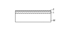
図1はこの発明の第1の実施形態に係る金属化合物膜の成膜方法の一例を概略的に示す流れ図、図2A〜図2Dはその主要な工程を概略的に示す断面図である。
(First embodiment)
<Film formation method>
FIG. 1 is a flowchart schematically showing an example of a method for forming a metal compound film according to the first embodiment of the present invention, and FIGS. 2A to 2D are sectional views schematically showing main steps thereof.
本例では、金属化合物膜としてハフニウムシリケート(以下HfSiOx)を成膜する例を示す。 In this example, an example of forming hafnium silicate (hereinafter referred to as HfSiOx) as a metal compound film is shown.
まず、図1のステップ1および図2Aに示すように、被処理体を準備する。被処理体の一例は、シリコンウエハWである。準備したシリコンウエハWは、成膜装置の処理室に収容される。 First, as shown in Step 1 of FIG. 1 and FIG. 2A, an object to be processed is prepared. An example of the object to be processed is a silicon wafer W. The prepared silicon wafer W is accommodated in the processing chamber of the film forming apparatus.
次に、図1のステップ2および図2Bに示すように、処理室に収容されたシリコンウエハWに物質Aを含む原料ガスを供給し、シリコンウエハW(被処理体)上に物質Aを吸着させる。本例では物質Aはハフニウム(以下Hf)であり、Hfを含む原料ガスの一例はテトラキス(ジメチルアミノ)ハフニウム(以下TDMAH)である。これにより、シリコンウエハW上にはHf吸着層1が形成される。吸着処理条件の一例は、次の通りである。
原 料 ガ ス: TDMAH
原料ガス流 量: 1g/min
処 理 圧 力: 13.3Pa〜266Pa(0.1〜2Torr)
処 理 温 度: 250℃
処 理 時 間: 30sec
(なお、本明細書においては、1Torrを133Paと定義する。)
次に、図1のステップ3に示すように、ステップ2に続けて、ステップ2を行なった処理室内を排気した後、この処理室内を、不活性ガスを用いてパージする。不活性ガスの一例は窒素(以下N2)ガスである。
Next, as shown in Step 2 and FIG. 2B of FIG. 1, a source gas containing the substance A is supplied to the silicon wafer W accommodated in the processing chamber, and the substance A is adsorbed on the silicon wafer W (object to be processed). Let In this example, the substance A is hafnium (hereinafter referred to as Hf), and an example of a source gas containing Hf is tetrakis (dimethylamino) hafnium (hereinafter referred to as TDMAH). Thereby, the Hf adsorption layer 1 is formed on the silicon wafer W. An example of the adsorption process conditions is as follows.
Raw material gas: TDMAH
Raw material gas flow rate: 1 g / min
Processing pressure: 13.3 Pa to 266 Pa (0.1 to 2 Torr)
Processing temperature: 250 ℃
Processing time: 30 sec
(In this specification, 1 Torr is defined as 133 Pa.)
Next, as shown in Step 3 of FIG. 1, following Step 2, the processing chamber in which Step 2 was performed is evacuated, and then the processing chamber is purged with an inert gas. An example of the inert gas is nitrogen (hereinafter, N 2 ) gas.
次に、図1のステップ4に示すように、ステップ2、3の繰り返し回数が、設定サイクル数か否かを判断する。設定サイクル数に達していない場合(No)には、ステップ2、3を繰り返す。設定サイクル数に達した場合(Yes)には、ステップ5に進む。 Next, as shown in step 4 of FIG. 1, it is determined whether or not the number of repetitions of steps 2 and 3 is the number of set cycles. If the set number of cycles has not been reached (No), steps 2 and 3 are repeated. If the set number of cycles has been reached (Yes), go to Step 5.
図1のステップ5および図2Cに示すように、Hfが吸着されたシリコンウエハWに物質Bを含む原料ガスを供給し、Hfが吸着されたシリコンウエハW(被処理体)上に物質Bを吸着させる。本例では物質Bはシリコン(以下Si)であり、Siを含む原料ガスの一例はジイソプロピルアミノシラン(DIPAS)である。これにより、Hf吸着層1が形成されたシリコンウエハW上にはSi吸着層2が形成される。吸着処理条件の一例は、次の通りである。
原 料 ガ ス: DIPAS
原料ガス流 量: 250sccm
処 理 圧 力: 13.3Pa〜13300Pa(0.1〜100Torr)
処 理 温 度: 250℃
処 理 時 間: 30sec
次に、図1のステップ6に示すように、ステップ5に続けて、ステップ5を行なった処理室内を排気した後、この処理室内を、不活性ガスを用いてパージする。不活性ガスの一例は窒素(以下N2)ガスである。
As shown in Step 5 of FIG. 1 and FIG. 2C, the source gas containing the substance B is supplied to the silicon wafer W on which Hf is adsorbed, and the substance B is put on the silicon wafer W (object to be processed) on which Hf is adsorbed. Adsorb. In this example, the substance B is silicon (hereinafter referred to as Si), and an example of a source gas containing Si is diisopropylaminosilane (DIPAS). Thereby, the Si adsorption layer 2 is formed on the silicon wafer W on which the Hf adsorption layer 1 is formed. An example of the adsorption process conditions is as follows.
Source Gas: DIPAS
Raw material gas flow rate: 250sccm
Processing pressure: 13.3 Pa to 13300 Pa (0.1 to 100 Torr)
Processing temperature: 250 ℃
Processing time: 30 sec
Next, as shown in Step 6 of FIG. 1, following Step 5, the processing chamber in which Step 5 was performed is evacuated, and then the processing chamber is purged with an inert gas. An example of the inert gas is nitrogen (hereinafter, N 2 ) gas.
次に、図1のステップ7に示すように、ステップ5、6の繰り返し回数が、設定サイクル数か否かを判断する。設定サイクル数に達していない場合(No)には、ステップ5、6を繰り返す。設定サイクル数に達した場合(Yes)には、ステップ8に進む。ステップ7における設定サイクル数は1回でも構わない。 Next, as shown in step 7 of FIG. 1, it is determined whether or not the number of repetitions of steps 5 and 6 is the set number of cycles. If the set number of cycles has not been reached (No), steps 5 and 6 are repeated. If the set number of cycles has been reached (Yes), the process proceeds to step 8. The number of set cycles in step 7 may be one.
図1のステップ8および図2Dに示すように、シリコンウエハW上に吸着されたHfおよびSiに対し、HfおよびSiとは異なった物質Cを化合させる。本例では物質Cは酸素(以下O)であり、化合は酸化である。酸化剤ガスの一例はオゾン(O3)ガスである。これにより、Hf吸着層1およびSi吸着層2は酸化され、HfSiOx層3となる。酸化処理条件の一例は、次の通りである。
酸化剤 ガ ス: O3
酸化剤ガス流量: 10000sccm
処 理 圧 力: 13.3Pa〜266Pa(0.1〜2Torr)
処 理 温 度: 250℃
処 理 時 間: 60sec
次に、図1のステップ9に示すように、ステップ8に続けて、ステップ8を行なった処理室内を排気した後、この処理室内を、不活性ガスを用いてパージする。不活性ガスの一例は窒素(以下N2)ガスである。
As shown in Step 8 of FIG. 1 and FIG. 2D, a substance C different from Hf and Si is combined with Hf and Si adsorbed on the silicon wafer W. In this example, the substance C is oxygen (hereinafter referred to as O), and the compound is oxidation. An example of the oxidant gas is ozone (O 3 ) gas. Thereby, the Hf adsorption layer 1 and the Si adsorption layer 2 are oxidized to become the HfSiOx layer 3. An example of the oxidation treatment condition is as follows.
Oxidizing agent gas: O 3
Oxidant gas flow rate: 10,000 sccm
Processing pressure: 13.3 Pa to 266 Pa (0.1 to 2 Torr)
Processing temperature: 250 ℃
Processing time: 60 sec
Next, as shown in Step 9 of FIG. 1, following Step 8, the processing chamber in which Step 8 was performed is evacuated, and then the processing chamber is purged with an inert gas. An example of the inert gas is nitrogen (hereinafter, N 2 ) gas.
ステップ8、9は1回のみで終了させても良いが、1回以上繰り返すことも可能である。1回以上繰り返すシーケンスとする場合には、ステップ10において、ステップ8、9の繰り返し回数が、設定サイクル数か否かを判断する。設定サイクル数に達していない場合(No)には、ステップ8、9を繰り返す。設定サイクル数に達した場合(Yes)には、ステップ11に進む。このシーケンスにおいて、ステップ10における設定サイクル数は1回でも構わない。 Steps 8 and 9 may be completed only once, but can be repeated one or more times. If the sequence is to be repeated one or more times, it is determined in step 10 whether the number of repetitions of steps 8 and 9 is the number of set cycles. If the set number of cycles has not been reached (No), Steps 8 and 9 are repeated. If the set number of cycles has been reached (Yes), the process proceeds to step 11. In this sequence, the number of set cycles in step 10 may be one.
次に、図1のステップ11に示すように、ステップ2〜9の繰り返し回数が、設定サイクル数か否かを判断する。設定サイクル数に達していない場合(No)には、HfSiOx層3の膜厚が設計膜厚に達していない、と判断する。よって、ステップ2〜9を繰り返す。設定サイクル数に達した場合(Yes)には、HfSiOx層3の膜厚が設計膜厚に達した、と判断する。よって、成膜処理を終了する。ステップ11における設定サイクル数はもちろん1回でも構わない。 Next, as shown in step 11 of FIG. 1, it is determined whether or not the number of repetitions of steps 2 to 9 is the set number of cycles. If the set number of cycles has not been reached (No), it is determined that the thickness of the HfSiOx layer 3 has not reached the design thickness. Therefore, steps 2 to 9 are repeated. When the set number of cycles has been reached (Yes), it is determined that the film thickness of the HfSiOx layer 3 has reached the design film thickness. Therefore, the film forming process is terminated. Of course, the number of set cycles in step 11 may be one.
本例において、ステップ2は、目的とするHfとSiとの組成比に応じて少なくとも2回以上繰り返され、ステップ5もまた、目的とするHfとSiとの組成比に応じて少なくとも1回以上行う。 In this example, step 2 is repeated at least twice according to the target composition ratio of Hf and Si, and step 5 is also at least once according to the target composition ratio of Hf and Si. Do.
このようにステップ2、およびステップ5を行うことにより、Hf吸着層1、およびSi吸着層2には、目的とするHfとSiとの組成比に応じた原子数分吸着させることが可能となる。そして、HfSiOx膜3が設計膜厚に達するまで、ステップ2〜9を繰り返すことで、金属化合物膜、本例ではHfSiOx膜3が成膜される。 By performing step 2 and step 5 in this manner, the Hf adsorption layer 1 and the Si adsorption layer 2 can be adsorbed by the number of atoms corresponding to the target composition ratio of Hf and Si. . Then, by repeating steps 2 to 9 until the HfSiOx film 3 reaches the designed film thickness, the metal compound film, in this example, the HfSiOx film 3 is formed.
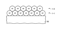
<第1の吸着モード>
図3A〜図3Eは、HfおよびSiの第1の吸着モードを模式的に示す図である。
まず、図3Aに示すように、例えば、ステップ2の1回で1原子層分のHf吸着層1が形成される、と仮定する。このステップ2を3回繰り返せば、図3Bおよび図3Cに示すように、Hf吸着層1は、Hf吸着層1−1〜1−3の3原子層分を得ることができる。
<First adsorption mode>
3A to 3E are diagrams schematically illustrating a first adsorption mode of Hf and Si.
First, as shown in FIG. 3A, for example, it is assumed that the Hf adsorption layer 1 for one atomic layer is formed in one step 2. If Step 2 is repeated three times, as shown in FIGS. 3B and 3C, the Hf adsorption layer 1 can obtain three atomic layers of Hf adsorption layers 1-1 to 1-3.
次に、図3Dに示すように、例えば、ステップ5の1回で1原子層分のSi吸着層2が形成される、と仮定する。このステップ1を、例えば、1回行えば、Si吸着層2は、Si吸着層2−1の1原子層分を得ることができる。また、特に図示はしないが、2回行えば、2原子層分のSi吸着層2を得ることができる。 Next, as shown in FIG. 3D, for example, it is assumed that the Si adsorbing layer 2 for one atomic layer is formed in one step 5. If this step 1 is performed once, for example, the Si adsorption layer 2 can obtain one atomic layer of the Si adsorption layer 2-1. Further, although not shown in particular, the Si adsorption layer 2 for two atomic layers can be obtained by performing twice.
このように、例えば、Hf吸着層1(1−1〜1−3)の積層数およびSi吸着層2(2−1)の積層数を、目的とするHfとSiとの組成比に応じて設定する。この後、図3Eに示すように、ステップ8において、Hf吸着層1(1−1〜1−3)およびSi吸着層2(2−1)を、例えば、酸化する。 Thus, for example, the number of stacks of the Hf adsorption layer 1 (1-1 to 1-3) and the number of stacks of the Si adsorption layer 2 (2-1) are set according to the target composition ratio of Hf and Si. Set. Thereafter, as shown in FIG. 3E, in step 8, the Hf adsorption layer 1 (1-1 to 1-3) and the Si adsorption layer 2 (2-1) are oxidized, for example.
このような吸着モードを持つ成膜方法によれば、例えば、Hf:Si=90:10〜95:5のように、極めてHfリッチなHfSiOx膜を得ることが可能となる。 According to the film forming method having such an adsorption mode, it is possible to obtain a very Hf-rich HfSiOx film, for example, Hf: Si = 90: 10 to 95: 5.
また、図3A〜図3Eに示す第1の吸着モード1回で、HfSiOx膜3の成膜を完了させることも可能であるが、図3A〜図3Eに示す第1の吸着モードを、HfSiOx膜3が設計された膜厚になるまで繰り返してもよい。いずれにしても、HfリッチなHfSiOx膜を得ることができる。 In addition, although it is possible to complete the formation of the HfSiOx film 3 by the first adsorption mode shown in FIGS. 3A to 3E, the first adsorption mode shown in FIGS. 3A to 3E is changed to the HfSiOx film. You may repeat until 3 becomes the designed film thickness. In any case, an Hf-rich HfSiOx film can be obtained.
<第2の吸着モード>
第1の吸着モードにおいては、Hf吸着層1(1−1〜1−3)の積層数およびSi吸着層2(2−1)の積層数を、目的とするHfとSiとの組成比に応じて設定した。第1の吸着モードは、HfSiOx膜の膜厚が厚い場合であっても適用できるモードである。
<Second adsorption mode>
In the first adsorption mode, the number of stacked Hf adsorption layers 1 (1-1 to 1-3) and the number of Si adsorption layers 2 (2-1) are set to the target composition ratio of Hf and Si. Set accordingly. The first adsorption mode is a mode that can be applied even when the HfSiOx film is thick.
第2の吸着モードは、HfSiOx膜の膜厚が薄い場合に適用できるモードである。具体的には、第2の吸着モードは、被処理体の表面の吸着サイト、例えば、シリコンウエハWの表面に存在する限られた数の吸着サイトに、HfおよびSiを吸着させていくモードである。 The second adsorption mode is a mode that can be applied when the thickness of the HfSiOx film is thin. Specifically, the second adsorption mode is a mode in which Hf and Si are adsorbed to adsorption sites on the surface of the workpiece, for example, a limited number of adsorption sites existing on the surface of the silicon wafer W. is there.
図4A〜図4Fは、HfおよびSiの第2の吸着モードを模式的に示す図である。
まず、図4Aに示すように、例えば、ステップ2の1回でシリコンウエハWの表面の吸着サイトのいくつかにHfが吸着される、と仮定する。このステップ2を、例えば3回繰り返していくと、図4Bおよび図4Cに示すように、HfをシリコンウエハWの表面の吸着サイトに、順次吸着させていくことができる。
4A to 4F are diagrams schematically showing a second adsorption mode of Hf and Si.
First, as shown in FIG. 4A, for example, it is assumed that Hf is adsorbed to some of the adsorption sites on the surface of the silicon wafer W in one step 2. If Step 2 is repeated three times, for example, Hf can be sequentially adsorbed on the adsorption sites on the surface of the silicon wafer W as shown in FIGS. 4B and 4C.
次に、図4Dに示すように、ステップ5において、SiをシリコンウエハWの表面の残された吸着サイトに吸着させる。ステップ2は1回行うだけでもよく、例えば、吸着しきれないならば、図4Eに示すように、2回以上行うようにしてもよい。 Next, as shown in FIG. 4D, in step 5, Si is adsorbed on the adsorption sites left on the surface of the silicon wafer W. Step 2 may be performed only once. For example, if it cannot be absorbed, it may be performed twice or more as shown in FIG. 4E.
このように、例えば、被処理体の表面の吸着サイト、例えば、シリコンウエハWの表面の吸着サイトを、目的とするHfとSiとの組成比に応じて、HfおよびSiで埋めていく。Hfの割合、およびSiの割合は、ステップ2の回数、ステップ5の回数に応じて設定することができる。この後、図4Fに示すように、ステップ8において、吸着されたHfおよびSiを、例えば、酸化する。これにより、例えば、Hf:Si
= 90:10〜95:5のように、極めてHfリッチなHfSiOx膜を、極めて薄い膜厚で得ることが可能となる。
Thus, for example, the adsorption site on the surface of the object to be processed, for example, the adsorption site on the surface of the silicon wafer W is filled with Hf and Si according to the target composition ratio of Hf and Si. The ratio of Hf and the ratio of Si can be set according to the number of times of step 2 and the number of times of step 5. Thereafter, as shown in FIG. 4F, in step 8, the adsorbed Hf and Si are oxidized, for example. Thus, for example, Hf: Si
= 90:10 to 95: 5 It is possible to obtain a very thin Hf-rich HfSiOx film with a very thin film thickness.
また、図4A〜図4Fに示す第2の吸着モード1回で、HfSiOx膜3の成膜を完了させることも可能である。しかし、第1の吸着モードと同様に、図4A〜図4Fに示す第2の吸着モードを、HfSiOx膜3が設計された膜厚になるまで繰り返してもよい。 In addition, it is possible to complete the formation of the HfSiOx film 3 in one second adsorption mode shown in FIGS. 4A to 4F. However, similarly to the first adsorption mode, the second adsorption mode shown in FIGS. 4A to 4F may be repeated until the HfSiOx film 3 has a designed film thickness.
なお、第1の吸着モードと第2の吸着モードとは、処理時間や原料ガスの流量等を調整することで切り換えることができる。例えば、処理時間を長くしたり、原料ガスの流量を多くしたりすると第1の吸着モードとなり、処理時間を短くしたり、原料ガスの流量を少なくしたりすると第2の吸着モードとなる。 The first adsorption mode and the second adsorption mode can be switched by adjusting the processing time, the flow rate of the source gas, and the like. For example, if the processing time is lengthened or the flow rate of the raw material gas is increased, the first adsorption mode is set. If the processing time is shortened or the flow rate of the raw material gas is decreased, the second adsorption mode is set.
また、特に、第2の吸着モードからも理解されるように、物質A(本例ではHf)と物質B(本例ではSi)のうち、金属化合物膜(本例ではHfSiOx膜)に含まれる割合を多くしたい物質については、先に吸着処理を行う物質Aとすることがよい。先に吸着処理をした方が、例えば、被処理体の表面の吸着サイトをより多く占有し易くなるためである。第1の実施形態においては、Hfの吸着処理の後、Siの吸着処理を行う。このため、HfリッチなHfSiOx膜3が得られる。これを、Siの吸着処理の後、Hfの吸着処理を行うようにすると、反対にSiリッチなHfSiOx膜3を得ることが可能となる。 In particular, as understood from the second adsorption mode, the metal compound film (HfSiOx film in this example) is included in the substance A (Hf in this example) and the substance B (Si in this example). About the substance which wants to increase a ratio, it is good to set it as the substance A which performs an adsorption process previously. This is because, when the adsorption treatment is performed first, for example, it becomes easier to occupy more adsorption sites on the surface of the object to be processed. In the first embodiment, after the Hf adsorption process, the Si adsorption process is performed. Therefore, the Hf-rich HfSiOx film 3 is obtained. If the Hf adsorption process is performed after the Si adsorption process, the Si-rich HfSiOx film 3 can be obtained.
このような第1の実施形態に係る金属化合物膜の成膜方法によれば、薄い膜厚の元であっても組成比の限界を拡げることができる。 According to the film forming method of the metal compound film according to the first embodiment, the limit of the composition ratio can be expanded even when the film thickness is thin.
また、組成比の調整については、上述したように、Hf吸着層およびSi吸着層の積層数や、例えば、被処理体の表面の吸着サイトへのHfおよびSiの吸着数で制御することができるので、組成比の調整に関する自由度を向上させることもできる。 The adjustment of the composition ratio can be controlled by the number of stacked Hf adsorption layers and Si adsorption layers, for example, the number of adsorption of Hf and Si to the adsorption site on the surface of the object to be processed, as described above. Therefore, the freedom degree regarding adjustment of a composition ratio can also be improved.
(第2の実施形態)
次に、この発明の第1の実施形態に係る金属化合物膜の成膜方法を実施することが可能な成膜装置の例を、この発明の第2の実施形態として説明する。
(Second Embodiment)
Next, an example of a film forming apparatus capable of performing the metal compound film forming method according to the first embodiment of the present invention will be described as a second embodiment of the present invention.
[成膜装置]
図5はこの発明の第2の実施形態に係る成膜装置の一例を概略的に示す断面図である。
[Film deposition system]
FIG. 5 is a sectional view schematically showing an example of a film forming apparatus according to the second embodiment of the present invention.
図5に示すように、成膜装置100は、下端が開口された有天井の円筒体状の処理室101を有している。処理室101の全体は、例えば、石英により形成されている。処理室101内の天井には、石英製の天井板102が設けられている。処理室101の下端開口部には、例えば、ステンレススチールにより円筒体状に成形されたマニホールド103がOリング等のシール部材104を介して連結されている。
As shown in FIG. 5, the
マニホールド103は処理室101の下端を支持している。マニホールド103の下方からは、被処理体として複数枚、例えば、50〜100枚の半導体基板、本例では、シリコンウエハWを多段に載置可能な石英製のウエハボート105が処理室101内に挿入可能となっている。これにより、処理室101内にシリコンウエハWが収容される。ウエハボート105は複数本の支柱106を有し、支柱106に形成された溝により複数枚のシリコンウエハWが支持されるようになっている。
The manifold 103 supports the lower end of the
ウエハボート105は、石英製の保温筒107を介してテーブル108上に載置されている。テーブル108は、マニホールド103の下端開口部を開閉する、例えば、ステンレススチール製の蓋部109を貫通する回転軸110上に支持される。回転軸110の貫通部には、例えば、磁性流体シール111が設けられ、回転軸110を気密にシールしつつ回転可能に支持している。蓋部109の周辺部とマニホールド103の下端部との間には、例えば、Oリングよりなるシール部材112が介設されている。これにより処理室101内のシール性が保持されている。回転軸110は、例えば、ボートエレベータ等の昇降機構(図示せず)に支持されたアーム113の先端に取り付けられている。これにより、ウエハボート105および蓋部109等は、一体的に昇降されて処理室101内に対して挿脱される。
The
成膜装置100は、処理室101内に、処理に使用するガスを供給する処理ガス供給機構114、及び処理室101内に、不活性ガスを供給する不活性ガス供給機構115を有している。
The
本例の処理ガス供給機構114は、物質Aを含む原料ガスとしてHf原料ガス供給源117a、物質Bを含む原料ガスとしてSi原料ガス供給源117b、および酸化剤ガス供給源117cを含んでいる。
The processing
不活性ガス供給機構115は、不活性ガス供給源120を含んでいる。
The inert
Hf原料ガスの一例はTDMAH、Si原料ガスの一例はDIPAS、酸化剤ガスの一例はオゾンガスである。不活性ガスの一例は窒素ガスである。不活性ガスは、パージガス等に利用される。 An example of the Hf source gas is TDMAH, an example of the Si source gas is DIPAS, and an example of the oxidizing gas is ozone gas. An example of the inert gas is nitrogen gas. The inert gas is used as a purge gas or the like.
Hf原料ガス供給源117aは、流量制御器121a及び開閉弁122aを介して、分散ノズル123aに接続されている。同様に、Si原料ガス供給源117b、および酸化剤ガス供給源117cは、流量制御器121b、121c、および開閉弁122b、122cを介して、分散ノズル123b(図5中には示されていないが開閉弁122bに接続される分散ノズル)、123cにそれぞれ接続されている。
The Hf source
分散ノズル123a〜123cは石英管よりなり、マニホールド103の側壁を内側へ貫通して上方向へ屈曲されて垂直に延びる。分散ノズル123a〜123cの垂直部分には、複数のガス吐出孔124が所定の間隔を隔てて形成されている。これにより、各ガスは、ガス吐出孔124から水平方向に処理室101内に向けて略均一に吐出される。
The
不活性ガス供給源120は、流量制御器121d、および開閉弁122dを介して、ノズル128に接続されている。ノズル128は、マニホールド103の側壁を貫通し、その先端から不活性ガスを、水平方向に処理室101内に向けて吐出させる。
The inert
処理室101内の、分散ノズル123a〜123cと反対側の部分には、処理室101内を排気するための排気口129が設けられている。排気口129は処理室101の側壁を上下方向へ削りとることによって細長く形成されている。処理室101の排気口129に対応する部分には、排気口129を覆うように断面がコの字状に成形された排気口カバー部材130が溶接により取り付けられている。排気口カバー部材130は、処理室101の側壁に沿って上方に延びており、処理室101の上方にガス出口131を規定している。ガス出口131には、真空ポンプ等を含む排気機構132が接続される。排気機構132は、処理室101内を排気することで処理に使用した処理ガスの排気、及び処理室101内の圧力を処理に応じた処理圧力とする。
An
処理室101の外周には筒体状の加熱装置133が設けられている。加熱装置133は、処理室101内に供給されたガスを活性化するとともに、処理室101内に収容された被処理体、本例ではシリコンウエハWを加熱する。
A
成膜装置100の各部の制御は、例えばマイクロプロセッサ(コンピュータ)からなるコントローラ150により行われる。コントローラ150には、オペレータが成膜装置100を管理するためにコマンドの入力操作等を行うタッチパネルや、成膜装置100の稼働状況を可視化して表示するディスプレイ等からなるユーザーインターフェース151が接続されている。
Control of each part of the
コントローラ150には記憶部152が接続されている。記憶部152は、成膜装置100で実行される各種処理をコントローラ150の制御にて実現するための制御プログラムや、処理条件に応じて成膜装置100の各構成部に処理を実行させるためのプログラムすなわちレシピが格納される。レシピは、例えば、記憶部152の中の記憶媒体に記憶される。記憶媒体は、ハードディスクや半導体メモリであってもよいし、CD-ROM、DVD、フラッシュメモリ等の可搬性のものであってもよい。また、他の装置から、例えば専用回線を介してレシピを適宜伝送させるようにしてもよい。レシピは、必要に応じて、ユーザーインターフェース151からの指示等にて記憶部152から読み出され、読み出されたレシピに従った処理をコントローラ150が実行することで、成膜装置100は、コントローラ150の制御のもと、所望の処理が実施される。
A
本例では、コントローラ150の制御のもと、上記第1の実施形態に係る金属化合物膜の成膜方法にしたがった成膜処理が順次実施される。
In this example, under the control of the
上記第1の実施形態に係る金属化合物膜の成膜方法は、図5に示すような成膜装置100を用いることによって、1台の成膜装置で形成することができる。
The metal compound film forming method according to the first embodiment can be formed by one film forming apparatus by using a
また、成膜装置としては図5に示すようなバッチ式に限らず、枚葉式の成膜装置であっても良い。 Further, the film forming apparatus is not limited to the batch type as shown in FIG. 5 and may be a single wafer type film forming apparatus.
(第3の実施形態)
次に、この発明の変形例のいくつかを、この発明の第3の実施形態として説明する。
(Third embodiment)
Next, some modified examples of the present invention will be described as a third embodiment of the present invention.
<パージガスについて>
まず、パージガスの変形例を説明する。
<Purge gas>
First, a modified example of the purge gas will be described.
上記第1の実施形態では、パージガスとして窒素ガスを用いた。これは窒素に限らず、不活性ガスであれば良い。例えば、アルゴンガス等の第18族元素(希ガス類)を用いることも可能である。 In the first embodiment, nitrogen gas is used as the purge gas. This is not limited to nitrogen, but may be an inert gas. For example, a Group 18 element (rare gas) such as argon gas can be used.
ただし、金属化合物膜として第1の実施形態のように、HfSiOx膜を成膜する場合には、パージガスに窒素ガスを用いることが好ましい。これは、HfSiOx膜に窒素を含有させることができ、窒素添加ハフニウムシリケート(HfSiON)膜とすることも可能となるためである。HfSiON膜によれば、HfSiOx膜に比較して、高温環境化での成分分離が少ない、という利点がある。 However, when the HfSiOx film is formed as the metal compound film as in the first embodiment, it is preferable to use nitrogen gas as the purge gas. This is because the HfSiOx film can contain nitrogen, and a nitrogen-added hafnium silicate (HfSiON) film can be obtained. According to the HfSiON film, there is an advantage that the component separation in a high temperature environment is less than that of the HfSiOx film.
<ステップ8:吸着された物質A、Bに物質Cを化合させる工程について>
次に、ステップ8の変形例を説明する。
<Step 8: Process of Combining Substance C with Adsorbed Substances A and B>
Next, a modified example of step 8 will be described.
ステップ8では、物質Cとしてオゾンガスを選択し、物質A、Bを酸化して金属化合物の酸化物とした。第1の実施形態では、HfSiOx膜3とした。 In step 8, ozone gas was selected as the substance C, and the substances A and B were oxidized to form an oxide of a metal compound. In the first embodiment, the HfSiOx film 3 is used.
酸化剤としては酸素を含むガスであればよく、オゾンガスの他、酸素(O2)ガス、水蒸気(H2O)等を挙げることができる。 The oxidizing agent may be any gas containing oxygen, and examples thereof include oxygen (O 2 ) gas, water vapor (H 2 O) and the like in addition to ozone gas.
酸化方法としては、第1の実施形態では熱を用いた熱酸化としたが、酸化剤ガスに含まれる酸素をプラズマ(ラジカル)化するプラズマ(ラジカル)酸化等も用いることが可能である。 As the oxidation method, thermal oxidation using heat is used in the first embodiment, but plasma (radical) oxidation or the like for converting oxygen contained in the oxidant gas into plasma (radical) can also be used.
また、酸化の他、窒化、又は酸窒化とすることも可能である。 Further, in addition to oxidation, nitridation or oxynitridation is also possible.
窒化剤としては窒素を含むガスであればよく、アンモニア(NH3)ガス等を挙げることができる。 The nitriding agent may be any gas containing nitrogen, and examples thereof include ammonia (NH 3 ) gas.
窒化方法としては、熱窒化の他、窒化剤ガスに含まれる窒素をプラズマ(ラジカル)化するプラズマ(ラジカル)窒化等も用いることができる。 As the nitriding method, plasma (radical) nitriding or the like for converting nitrogen contained in the nitriding agent gas into plasma (radical) can be used in addition to thermal nitriding.
酸窒化剤としては、窒素酸化物(NOx)を挙げることができる。また、酸窒化に際しては上記酸化剤および上記窒化剤を同時に処理室内に供給するようにしても良い。 An example of the oxynitriding agent is nitrogen oxide (NOx). In the oxynitriding, the oxidizing agent and the nitriding agent may be simultaneously supplied into the processing chamber.
また、酸窒化方法は、酸化および窒化と同様に、熱を用いた熱酸窒化の他、窒素および酸素をプラズマ(ラジカル)化するプラズマ(ラジカル)酸窒化等を用いることができる。 As the oxynitriding method, in addition to thermal oxynitridation using heat, plasma (radical) oxynitridation that converts nitrogen and oxygen into plasma (radical) can be used, as in oxidation and nitridation.
<金属について>
次に、金属に関する変形例を説明する。
<About metal>
Next, the modification regarding a metal is demonstrated.
第1の実施形態では、金属としてHfを選んだ。また、Hf原料ガスとしてTDMAHを選んだ。Hf原料ガスとしては、
TDMAH(テトラキス(ジメチルアミノ)ハフニウム)
TEMAH(テトラキス(エチルメチルアミノ)ハフニウム)
TDEAH(テトラキス(ジエチルアミノ)ハフニウム)
トリス(ジメチルアミノ)シクロペンタジエニルハフニウム
のいずれか一つを含むガスを選ぶことができる。
In the first embodiment, Hf is selected as the metal. Further, TDMAH was selected as the Hf source gas. As Hf source gas,
TDMAH (Tetrakis (dimethylamino) hafnium)
TEMAH (tetrakis (ethylmethylamino) hafnium)
TDEAH (tetrakis (diethylamino) hafnium)
A gas containing any one of tris (dimethylamino) cyclopentadienyl hafnium can be selected.
また、物質Aおよび物質Bの一方の金属としては、
ハフニウム(Hf)
ジルコニウム(Zr)
チタン(Ti)
アルミニウム(Al)
の少なくともいずれか一つを選ぶことができる。
Moreover, as one metal of the substance A and the substance B,
Hafnium (Hf)
Zirconium (Zr)
Titanium (Ti)
Aluminum (Al)
You can choose at least one of
また、Zrを含む原料ガスとしては、
TEMAZ(テトラキス(エチルメチルアミノ)ジルコニウム)
トリス(ジメチルアミノ)シクロペンタジエニルジルコニウム
のいずれか一つを含むガスを選ぶことができる。
Moreover, as source gas containing Zr,
TEMAZ (tetrakis (ethylmethylamino) zirconium)
A gas containing any one of tris (dimethylamino) cyclopentadienylzirconium can be selected.
また、Tiを含むガスとしては
TiCl4(四塩化チタン)
ペンタメチルシクロペンタジエニルチタントリメトキシド
メチルシクロペンタジエニルトリスジメチルアミノチタン
のいずれか一つを含むガスを選ぶことができる。
In addition, as a gas containing Ti, TiCl 4 (titanium tetrachloride)
Pentamethylcyclopentadienyl titanium trimethoxide A gas containing any one of methylcyclopentadienyl trisdimethylamino titanium can be selected.
また、Alを含むガスとして
TMA(トリメチルアルミニウム)
を含むガスを選ぶことができる。
TMA (trimethylaluminum) as a gas containing Al
You can choose gas containing.
<Siについて>
第1の実施形態では、物質Aおよび物質のいずれかにSiを用いた。Si原料ガスとしては、
2DMAS(ビス(ジメチルアミノ)シラン)
3DMAS(トリス(ジメチルアミノ)シラン)
4DMAS(テトラキス(ジメチルアミノ)シラン)
DIPAS(ジイソプロピルアミノシラン)
のいずれか一つを含むガスを選ぶことができる。
<About Si>
In the first embodiment, Si is used for either the substance A or the substance. As Si source gas,
2DMAS (bis (dimethylamino) silane)
3DMAS (Tris (dimethylamino) silane)
4DMAS (tetrakis (dimethylamino) silane)
DIPAS (Diisopropylaminosilane)
A gas containing any one of the above can be selected.
また、第1の実施形態ではSiを選んだが、炭素(C)、ゲルマニウム(Ge)などの他の第IV族元素(IUPAC式長周期表の第14族元素)に変更することも可能である。 Further, although Si is selected in the first embodiment, it can be changed to another group IV element (group 14 element in the IUPAC long periodic table) such as carbon (C) or germanium (Ge). .
<金属化合物膜の応用用途>
次に、第1の実施形態に従って成膜された金属化合物膜の応用用途を説明する。
<Application of metal compound film>
Next, application uses of the metal compound film formed according to the first embodiment will be described.
例えば、HfSiOxは、SiO2に比較して高い比誘電率を持つHigh−k(高誘電率)材料である。このため、電子製品、例えば、半導体集積回路装置やフラットパネルディスプレイのトランジスタのゲート絶縁膜や、キャパシタの誘電体膜として利用することが可能である。特に、第1の実施形態に従って成膜された金属化合物膜、例えば、HfSiOx膜は、薄膜化しても、その組成比の限界を拡げることができ、かつ、組成比の調整に関する自由度が高い。このため、非常に薄い、例えば、50nm以下の有限値を持つゲート絶縁膜およびキャパシタの誘電体膜としての利用に有利である。 For example, HfSiOx is a High-k (high dielectric constant) material having a higher relative dielectric constant than SiO 2 . Therefore, it can be used as a gate insulating film of a transistor of an electronic product, for example, a semiconductor integrated circuit device or a flat panel display, or a dielectric film of a capacitor. In particular, even if the metal compound film formed according to the first embodiment, for example, the HfSiOx film, is thinned, the limit of the composition ratio can be expanded, and the degree of freedom regarding the adjustment of the composition ratio is high. Therefore, it is advantageous for use as a very thin gate insulating film having a finite value of, for example, 50 nm or less and a dielectric film of a capacitor.
特に、10nm未満の有限値を持つゲート絶縁膜およびキャパシタの誘電体膜であっても、第1の実施形態に係る金属化合物膜の成膜方法によれば、Hf:Siの組成比が90:10のHfSiOx膜を成膜することもできる。 In particular, even in the case of a gate insulating film and a capacitor dielectric film having a finite value of less than 10 nm, the Hf: Si composition ratio is 90: according to the metal compound film forming method according to the first embodiment. Ten HfSiOx films can also be formed.
このように、第1の実施形態に従って成膜された金属化合物膜は、電子製品、例えば、半導体集積回路装置やフラットパネルディスプレイのゲート絶縁膜や、キャパシタの誘電体膜として利用に好適である。 As described above, the metal compound film formed according to the first embodiment is suitable for use as an electronic product, for example, a gate insulating film of a semiconductor integrated circuit device or a flat panel display, or a dielectric film of a capacitor.
以上、この発明を第1〜第3の実施形態に従って説明したが、この発明は、上記第1〜第3の実施形態に限定されることは無く、その趣旨を逸脱しない範囲で種々変形可能である。 As mentioned above, although this invention was demonstrated according to 1st-3rd embodiment, this invention is not limited to the said 1st-3rd embodiment, A various deformation | transformation is possible in the range which does not deviate from the meaning. is there.
例えば、上記実施形態においては、処理条件を具体的に例示したが、処理条件は、上記具体的な例示に限られるものではなく、例えば、処理室内の容積等に応じて、適宜変更が可能である。
その他、この発明はその要旨を逸脱しない範囲で様々に変形することができる。
For example, in the above embodiment, the processing conditions are specifically exemplified, but the processing conditions are not limited to the above specific examples, and can be appropriately changed according to, for example, the volume in the processing chamber. is there.
In addition, the present invention can be variously modified without departing from the gist thereof.
W…シリコンウエハ、1、1−1〜1−3…Hf吸着層、2、2−1…Si吸着層、3…HfSiOx膜。 W ... silicon wafer, 1, 1-1 to 1-3 ... Hf adsorption layer, 2, 2-1 ... Si adsorption layer, 3 ... HfSiOx film.
Claims (16)
(1) 前記処理室内に前記物質Aを含む原料ガスを供給して、前記被処理体上の吸着サイトに部分的に前記物質Aを吸着させるステップと、前記処理室内をパージするステップとを、前記物質Aおよび前記物質Bの組成比に応じて2回以上繰り返し、前記吸着サイトに所定量の前記物質Aを吸着させる段階と、
(2) 前記(1)の段階の後、前記処理室内に前記物質Bを含む原料ガスを供給して、前記吸着サイトに部分的に前記物質Bを吸着させるステップと、前記処理室内をパージするステップとを、前記物質Aおよび前記物質Bの組成比に応じて1回または2回以上繰り返し、前記吸着サイトの残部に所定量の前記物質Bを吸着させる段階と、
(3) 前記(2)の段階の後、前記処理室内に前記物質A、Bとは異なる物質Cを供給して、前記物質A、Bに前記物質Cを化合させるステップと、前記処理室内をパージするステップとを1回または2回以上繰り返す段階と
を含み、
前記(1)〜(3)の段階により、前記所定組成の前記金属化合物膜を形成し、前記(1)〜(3)の段階を前記所定組成の前記金属化合物膜が設計膜厚となるまで1回または2回以上の所定回数行うことを特徴とする金属化合物膜の成膜方法。 In a processing chamber, a metal compound film including a substance A and a substance B, one of which is a metal, and having a predetermined composition in which the ratio of the substance A is higher than the ratio of the substance B is formed on a target object. A method of forming a metal compound film,
(1) supplying a source gas containing the substance A into the processing chamber to partially adsorb the substance A at an adsorption site on the object to be processed; and purging the processing chamber; the substance a and to repeat more than once in accordance with the composition ratio of the material B, a step of adsorbing the substance a predetermined amount of the adsorption sites,
(2) After the step (1), supplying a source gas containing the substance B into the processing chamber to partially adsorb the substance B on the adsorption site, and purging the processing chamber and a step, to repeat one or more times depending on the composition ratio of the substance a and the substance B, the steps of adsorbing the substance B of a predetermined amount to the remainder of the adsorption sites,
(3) After the step (2), supplying a substance C different from the substances A and B into the processing chamber to combine the substance C with the substances A and B; Repeating the step of purging once or twice or more,
The metal compound film having the predetermined composition is formed by the steps (1) to (3), and the steps (1) to (3) are performed until the metal compound film having the predetermined composition reaches a design film thickness. A method of forming a metal compound film, which is performed once or twice a predetermined number of times.
ハフニウム
ジルコニウム
チタン
アルミニウム
の少なくともいずれか一つが選ばれることを特徴とする請求項1から請求項3のいずれか一項に記載の金属化合物膜の成膜方法。 One of the substance A and the substance B is
The method for forming a metal compound film according to any one of claims 1 to 3, wherein at least one of hafnium, zirconium, titanium, and aluminum is selected.
TDMAH(テトラキス(ジメチルアミノ)ハフニウム)
TEMAH(テトラキス(エチルメチルアミノ)ハフニウム)
TDEAH(テトラキス(ジエチルアミノ)ハフニウム)
トリス(ジメチルアミノ)シクロペンタジエニルハフニウム
のいずれか一つを含むガスが選ばれ、
前記ジルコニウムを含む原料ガスとして
TEMAZ(テトラキス(エチルメチルアミノ)ジルコニウム)
トリス(ジメチルアミノ)シクロペンタジエニルジルコニウム
のいずれか一つを含むガスが選ばれ、
前記チタンを含むガスとして
TiCl4(四塩化チタン)
ペンタメチルシクロペンタジエニルチタントリメトキシド
メチルシクロペンタジエニルトリスジメチルアミノチタン
のいずれか一つを含むガスが選ばれ、
前記アルミニウムを含むガスとして
TMA(トリメチルアルミニウム)
を含むガスが選ばれることを特徴とする請求項4に記載の金属化合物膜の成膜方法。 TDMAH (tetrakis (dimethylamino) hafnium) as the source gas containing hafnium
TEMAH (tetrakis (ethylmethylamino) hafnium)
TDEAH (tetrakis (diethylamino) hafnium)
A gas containing any one of tris (dimethylamino) cyclopentadienylhafnium is selected,
As a raw material gas containing zirconium, TEMAZ (tetrakis (ethylmethylamino) zirconium)
A gas containing any one of tris (dimethylamino) cyclopentadienylzirconium is selected,
As the gas containing titanium, TiCl 4 (titanium tetrachloride)
Gas containing any one of pentamethylcyclopentadienyl titanium trimethoxide methylcyclopentadienyl trisdimethylamino titanium is selected,
TMA (trimethylaluminum) as the gas containing aluminum
The method of forming a metal compound film according to claim 4, wherein a gas containing a metal is selected.
第IV族元素
の一つが選ばれることを特徴とする請求項4又は請求項5に記載の金属化合物膜の成膜方法。 In the other of the substance A and the substance B,
6. The method of forming a metal compound film according to claim 4, wherein one of the group IV elements is selected.
2DMAS(ビス(ジメチルアミノ)シラン)
3DMAS(トリス(ジメチルアミノ)シラン)
4DMAS(テトラキス(ジメチルアミノ)シラン)
DIPAS(ジイソプロピルアミノシラン)
のいずれか一つを含むガスが選ばれることを特徴とする請求項7に記載の金属化合物膜の成膜方法。 As the source gas containing silicon,
2DMAS (bis (dimethylamino) silane)
3DMAS (Tris (dimethylamino) silane)
4DMAS (tetrakis (dimethylamino) silane)
DIPAS (Diisopropylaminosilane)
The method of forming a metal compound film according to claim 7, wherein a gas containing any one of the above is selected.
(1) 前記処理室内にHfを含む原料ガスを供給して、前記被処理体上の吸着サイトに対して部分的にHfを吸着させるステップと、前記処理室内をパージするステップとを、HfおよびSiの組成比に応じて2回以上繰り返し、前記吸着サイトに所定量のHfを吸着させる段階と、
(2) 前記処理室内にSiを含む原料ガスを供給して、被処理体上の前記吸着サイトに部分的にSiを吸着させるステップと、前記処理室内をパージするステップとを、HfおよびSiの組成比に応じて1回または2回以上繰り返し、前記吸着サイトの残部に所定量のSiを吸着させる段階と、
(3) 前記(1)段階および(2)段階を行った後、前記処理室内にHfおよびSiを酸化する酸化剤を供給して、HfおよびSiを酸化させるステップと、前記処理室内をパージするステップとを1回または2回以上繰り返す段階と
を含み、
前記(1)〜(3)の段階により前記所定組成のHfSiOx膜を形成し、前記(1)〜(3)の段階を前記所定組成のHfSiOx膜が設計膜厚となるまで1回または2回以上の所定回数行うことを特徴とする金属化合物膜の成膜方法。 A metal compound film forming method for forming a Hf-rich HfSiOx film having a predetermined composition as a metal compound film on a target object in a processing chamber,
(1) supplying a source gas containing Hf into the processing chamber to partially adsorb Hf to an adsorption site on the object to be processed; and purging the processing chamber with Hf and it repeating two or more times depending on the composition ratio of Si, the steps of adsorbing a predetermined amount of Hf in the adsorption sites,
(2) supplying a source gas containing Si into the processing chamber to partially adsorb Si at the adsorption site on the object to be processed; and purging the processing chamber; it repeating one or more times depending on the composition ratio, the steps of adsorbing a predetermined amount of Si to the remainder of the adsorption sites,
(3) After performing the steps (1) and (2), supplying an oxidizing agent for oxidizing Hf and Si into the processing chamber to oxidize Hf and Si, and purging the processing chamber Repeating the step once or twice or more,
The HfSiOx film having the predetermined composition is formed by the steps (1) to (3), and the steps (1) to (3) are performed once or twice until the HfSiOx film having the predetermined composition reaches the design film thickness. A metal compound film forming method characterized by performing the above predetermined number of times.
TDMAH(テトラキス(ジメチルアミノ)ハフニウム)
TEMAH(テトラキス(エチルメチルアミノ)ハフニウム)
TDEAH(テトラキス(ジエチルアミノ)ハフニウム)
トリス(ジメチルアミノ)シクロペンタジエニルハフニウム
のいずれか一つを含むガスが選ばれ、
前記シリコンを含む原料ガスとして、
2DMAS(ビス(ジメチルアミノ)シラン)
3DMAS(トリス(ジメチルアミノ)シラン)
4DMAS(テトラキス(ジメチルアミノ)シラン)
DIPAS(ジイソプロピルアミノシラン)
のいずれか一つを含むガスが選ばれることを特徴とする請求項9から請求項11のいずれか一項に記載の金属化合物の成膜方法。 TDMAH (tetrakis (dimethylamino) hafnium) as the source gas containing hafnium
TEMAH (tetrakis (ethylmethylamino) hafnium)
TDEAH (tetrakis (diethylamino) hafnium)
A gas containing any one of tris (dimethylamino) cyclopentadienylhafnium is selected,
As the source gas containing silicon,
2DMAS (bis (dimethylamino) silane)
3DMAS (Tris (dimethylamino) silane)
4DMAS (tetrakis (dimethylamino) silane)
DIPAS (Diisopropylaminosilane)
12. The method of forming a metal compound according to claim 9, wherein a gas containing any one of the above is selected.
前記金属化合物膜の成膜処理を施す処理室と、
前記処理室内に、前記物質Aを含むガスを供給する物質A原料ガス供給機構と、
前記処理室内に、前記物質Bを含むガスを供給する物質B原料ガス供給機構と、
前記処理室内に、前記物質A、Bとは異なった物質Cを供給する物質C原料ガス供給機構と、
前記処理室内に、パージガスとして不活性ガスを供給する不活性ガス供給機構と、
前記処理室内を排気する排気機構と、
前記成膜装置を制御する制御装置と、
を具備し、
前記制御装置が、請求項1から請求項8のいずれか一項に記載の金属化合物膜の成膜方法を実施することを特徴とする成膜装置。 A metal compound film deposition apparatus for accommodating a target object and forming a metal compound film containing a substance A and a substance B, one of which is a metal, on the stored target object. And
A processing chamber for performing a film forming process of the metal compound film;
A substance A source gas supply mechanism for supplying a gas containing the substance A into the processing chamber;
A substance B source gas supply mechanism for supplying a gas containing the substance B into the processing chamber;
A substance C source gas supply mechanism for supplying a substance C different from the substances A and B into the processing chamber;
An inert gas supply mechanism for supplying an inert gas as a purge gas into the processing chamber;
An exhaust mechanism for exhausting the processing chamber;
A control device for controlling the film forming apparatus;
Comprising
A film forming apparatus, wherein the control device implements the metal compound film forming method according to claim 1.
Priority Applications (3)
| Application Number | Priority Date | Filing Date | Title |
|---|---|---|---|
| JP2012270670A JP6087609B2 (en) | 2012-12-11 | 2012-12-11 | Metal compound film forming method, film forming apparatus, and electronic product manufacturing method |
| KR1020130153352A KR101761449B1 (en) | 2012-12-11 | 2013-12-10 | Method and apparatus of forming metal compound film, and electronic product |
| US14/102,792 US9234275B2 (en) | 2012-12-11 | 2013-12-11 | Method and apparatus of forming metal compound film, and electronic product |
Applications Claiming Priority (1)
| Application Number | Priority Date | Filing Date | Title |
|---|---|---|---|
| JP2012270670A JP6087609B2 (en) | 2012-12-11 | 2012-12-11 | Metal compound film forming method, film forming apparatus, and electronic product manufacturing method |
Publications (2)
| Publication Number | Publication Date |
|---|---|
| JP2014116517A JP2014116517A (en) | 2014-06-26 |
| JP6087609B2 true JP6087609B2 (en) | 2017-03-01 |
Family
ID=50881155
Family Applications (1)
| Application Number | Title | Priority Date | Filing Date |
|---|---|---|---|
| JP2012270670A Active JP6087609B2 (en) | 2012-12-11 | 2012-12-11 | Metal compound film forming method, film forming apparatus, and electronic product manufacturing method |
Country Status (3)
| Country | Link |
|---|---|
| US (1) | US9234275B2 (en) |
| JP (1) | JP6087609B2 (en) |
| KR (1) | KR101761449B1 (en) |
Families Citing this family (7)
| Publication number | Priority date | Publication date | Assignee | Title |
|---|---|---|---|---|
| WO2017086630A1 (en) * | 2015-11-19 | 2017-05-26 | 주식회사 유진테크 머티리얼즈 | Precursor composition containing group iv organic compound and method for forming thin film using same |
| CN115233183A (en) | 2017-05-16 | 2022-10-25 | Asm Ip 控股有限公司 | Selective PEALD of oxide on dielectric |
| KR20190005741A (en) * | 2017-07-07 | 2019-01-16 | 도쿄엘렉트론가부시키가이샤 | Method of manufacturing semiconductor device and method of forming metal oxide film |
| JP6654232B2 (en) * | 2018-12-25 | 2020-02-26 | 株式会社Kokusai Electric | Semiconductor device manufacturing method, substrate processing apparatus, and program |
| JP2021169649A (en) * | 2020-04-15 | 2021-10-28 | 東京エレクトロン株式会社 | Method for forming metal nitride film, and apparatus |
| JP2022055634A (en) | 2020-09-29 | 2022-04-08 | 東京エレクトロン株式会社 | Film deposition method and film deposition apparatus |
| CN112928210B (en) * | 2021-02-03 | 2022-04-15 | 长鑫存储技术有限公司 | Capacitor structure and preparation method thereof |
Family Cites Families (20)
| Publication number | Priority date | Publication date | Assignee | Title |
|---|---|---|---|---|
| KR100385946B1 (en) * | 1999-12-08 | 2003-06-02 | 삼성전자주식회사 | Method for forming a metal layer by an atomic layer deposition and a semiconductor device with the metal layer as a barrier metal layer, an upper electrode, or a lower electrode of capacitor |
| US6984591B1 (en) | 2000-04-20 | 2006-01-10 | International Business Machines Corporation | Precursor source mixtures |
| EP1256638B1 (en) * | 2001-05-07 | 2008-03-26 | Samsung Electronics Co., Ltd. | Method of forming a multi-components thin film |
| KR100474847B1 (en) * | 2001-05-07 | 2005-03-08 | 삼성전자주식회사 | Thin film comprising multi components and method for forming the same |
| JP4007044B2 (en) * | 2002-04-19 | 2007-11-14 | ソニー株式会社 | Thin film formation method using atomic layer deposition |
| TW200408015A (en) | 2002-08-18 | 2004-05-16 | Asml Us Inc | Atomic layer deposition of high K metal silicates |
| CN1689147A (en) | 2003-04-17 | 2005-10-26 | 富士通株式会社 | Method for forming high dielectric film |
| KR100555543B1 (en) * | 2003-06-24 | 2006-03-03 | 삼성전자주식회사 | Method for forming high dielectric layer by atomic layer deposition and method for manufacturing capacitor having the layer |
| US20050056219A1 (en) | 2003-09-16 | 2005-03-17 | Tokyo Electron Limited | Formation of a metal-containing film by sequential gas exposure in a batch type processing system |
| JP4059183B2 (en) | 2003-10-07 | 2008-03-12 | ソニー株式会社 | Insulator thin film manufacturing method |
| US20050252449A1 (en) | 2004-05-12 | 2005-11-17 | Nguyen Son T | Control of gas flow and delivery to suppress the formation of particles in an MOCVD/ALD system |
| US7651729B2 (en) * | 2004-05-14 | 2010-01-26 | Samsung Electronics Co., Ltd. | Method of fabricating metal silicate layer using atomic layer deposition technique |
| JP2007088113A (en) | 2005-09-21 | 2007-04-05 | Sony Corp | Manufacturing method of semiconductor device |
| CN101288162B (en) * | 2005-10-14 | 2010-06-09 | 日本电气株式会社 | Method and apparatus for manufacturing semiconductor device |
| US7795160B2 (en) | 2006-07-21 | 2010-09-14 | Asm America Inc. | ALD of metal silicate films |
| KR101427142B1 (en) * | 2006-10-05 | 2014-08-07 | 에이에스엠 아메리카, 인코포레이티드 | ALD of metal silicate films |
| JP2010283040A (en) * | 2009-06-02 | 2010-12-16 | Panasonic Corp | Semiconductor device and method of manufacturing the same |
| JPWO2011093203A1 (en) * | 2010-01-29 | 2013-06-06 | 株式会社日立国際電気 | Semiconductor device manufacturing method, substrate processing apparatus, and semiconductor device |
| KR101147728B1 (en) * | 2010-08-02 | 2012-05-25 | 주식회사 유진테크 | Method of cyclic deposition thin film |
| JP2012059834A (en) * | 2010-09-07 | 2012-03-22 | Hitachi Kokusai Electric Inc | Method for manufacturing semiconductor device |
-
2012
- 2012-12-11 JP JP2012270670A patent/JP6087609B2/en active Active
-
2013
- 2013-12-10 KR KR1020130153352A patent/KR101761449B1/en active IP Right Grant
- 2013-12-11 US US14/102,792 patent/US9234275B2/en active Active
Also Published As
| Publication number | Publication date |
|---|---|
| JP2014116517A (en) | 2014-06-26 |
| KR20140075623A (en) | 2014-06-19 |
| US9234275B2 (en) | 2016-01-12 |
| KR101761449B1 (en) | 2017-07-25 |
| US20140161706A1 (en) | 2014-06-12 |
Similar Documents
| Publication | Publication Date | Title |
|---|---|---|
| JP6087609B2 (en) | Metal compound film forming method, film forming apparatus, and electronic product manufacturing method | |
| JP6267080B2 (en) | Method and apparatus for forming silicon nitride film | |
| TWI529835B (en) | Film forming method and film forming apparatus | |
| JP6246558B2 (en) | Silicon oxycarbonitride film, silicon oxycarbide film, silicon oxynitride film forming method and film forming apparatus | |
| JP5882075B2 (en) | Capacitor manufacturing method, capacitor, and dielectric film forming method used therefor | |
| JP5258229B2 (en) | Film forming method and film forming apparatus | |
| TWI552225B (en) | Sicn film formation method and apparatus | |
| TWI447257B (en) | Method of manufacturing semiconductor device, substrate processing method and substrate processing apparatus | |
| KR100861851B1 (en) | Method and apparatus for forming silicon oxide film | |
| JP5661262B2 (en) | Film forming method and film forming apparatus | |
| US20150364318A1 (en) | Method for manufacturing semiconductor device, method for processing substrate, substrate processing apparatus and recording medium | |
| KR20110009624A (en) | Batch cvd method and apparatus for semiconductor process, and computer readable storage medium | |
| TW201438061A (en) | Method for manufacturing semiconductor device, substrate processing device, and recording medium | |
| KR101552856B1 (en) | Film formation method and film formation apparatus | |
| JP5221089B2 (en) | Film forming method, film forming apparatus, and storage medium | |
| KR102068879B1 (en) | TiN-BASED FILM AND TiN-BASED FILM FORMING METHOD | |
| US20110281443A1 (en) | Film formation method and film formation apparatus | |
| JP5675458B2 (en) | Film forming method, film forming apparatus, and storage medium | |
| KR20150142590A (en) | FILM FORMING METHOD OF SiCN FILM | |
| JP2016186992A (en) | Substrate processing device, method of manufacturing semiconductor device, and program | |
| JP6452787B2 (en) | Method and apparatus for forming silicon oxycarbonitride film | |
| KR101501038B1 (en) | Method of depositing silicon oxide film and silicon nitride film, film forming apparatus, and method of manufacturing semiconductor device | |
| JP6345136B2 (en) | Method and apparatus for forming carbon-containing silicon nitride film | |
| JP2014064039A (en) | Film deposition method and film deposition device |
Legal Events
| Date | Code | Title | Description |
|---|---|---|---|
| A621 | Written request for application examination |
Free format text: JAPANESE INTERMEDIATE CODE: A621 Effective date: 20150417 |
|
| A977 | Report on retrieval |
Free format text: JAPANESE INTERMEDIATE CODE: A971007 Effective date: 20160223 |
|
| A131 | Notification of reasons for refusal |
Free format text: JAPANESE INTERMEDIATE CODE: A131 Effective date: 20160315 |
|
| A521 | Request for written amendment filed |
Free format text: JAPANESE INTERMEDIATE CODE: A523 Effective date: 20160511 |
|
| A131 | Notification of reasons for refusal |
Free format text: JAPANESE INTERMEDIATE CODE: A131 Effective date: 20161108 |
|
| A521 | Request for written amendment filed |
Free format text: JAPANESE INTERMEDIATE CODE: A523 Effective date: 20170106 |
|
| TRDD | Decision of grant or rejection written | ||
| A01 | Written decision to grant a patent or to grant a registration (utility model) |
Free format text: JAPANESE INTERMEDIATE CODE: A01 Effective date: 20170131 |
|
| A61 | First payment of annual fees (during grant procedure) |
Free format text: JAPANESE INTERMEDIATE CODE: A61 Effective date: 20170202 |
|
| R150 | Certificate of patent or registration of utility model |
Ref document number: 6087609 Country of ref document: JP Free format text: JAPANESE INTERMEDIATE CODE: R150 |
|
| R250 | Receipt of annual fees |
Free format text: JAPANESE INTERMEDIATE CODE: R250 |
|
| R250 | Receipt of annual fees |
Free format text: JAPANESE INTERMEDIATE CODE: R250 |
|
| R250 | Receipt of annual fees |
Free format text: JAPANESE INTERMEDIATE CODE: R250 |
|
| R250 | Receipt of annual fees |
Free format text: JAPANESE INTERMEDIATE CODE: R250 |
|
| R250 | Receipt of annual fees |
Free format text: JAPANESE INTERMEDIATE CODE: R250 |