JP2004289082A - Method of forming high-dielectric-constant gate insulating film - Google Patents
Method of forming high-dielectric-constant gate insulating film Download PDFInfo
- Publication number
- JP2004289082A JP2004289082A JP2003082424A JP2003082424A JP2004289082A JP 2004289082 A JP2004289082 A JP 2004289082A JP 2003082424 A JP2003082424 A JP 2003082424A JP 2003082424 A JP2003082424 A JP 2003082424A JP 2004289082 A JP2004289082 A JP 2004289082A
- Authority
- JP
- Japan
- Prior art keywords
- film
- gas
- dielectric constant
- high dielectric
- insulating film
- Prior art date
- Legal status (The legal status is an assumption and is not a legal conclusion. Google has not performed a legal analysis and makes no representation as to the accuracy of the status listed.)
- Pending
Links
Images


Abstract
Description
【0001】
【発明の属する技術分野】
本発明はシリコン半導体装置、特に高誘電率ゲート絶縁膜の形成方法に関するものである。
【0002】
【従来の技術】
近年の半導体装置における高集積化及び高速化に対する技術進展に伴い、MOSFETの微細化が進められている。微細化に伴いゲート絶縁膜の薄膜化を進めると、トンネル電流によるゲートリーク電流の増大といった問題が顕在化してくる。この問題を抑制するために、ゲート絶縁膜にHfO2やZrO2などの高誘電率材料を用いたゲート絶縁膜(以下、High−Kゲート絶縁膜と称す)により、薄いSiO2換算膜厚(EOT)を実現しながら物理的な膜厚を厚くするという手法が研究されている。従来のHigh−Kゲート絶縁膜の形成方法としては次のものが知られている(非特許文献1参照)。
【0003】
以下、従来例について図6を参照しながら説明する。図6は従来例のプロセスフロー図である。まず、Si基板を用い、標準RCA洗浄、フッ酸による洗浄後に、NH3ガスで700℃10秒の処理でシリコン窒化膜の界面層を形成する。次に、N2ガスをC16H36HfO4のキャリアガスとして使用し、酸素ガスと混合して500℃で3分のCVD(Chemical Vapor Deposition)処理で、4nm程度の膜厚のHfO2膜を堆積する。堆積後の熱処理は、N2ガス中で700℃から900℃の温度範囲で30秒のアニール処理(ポストデポジションアニール処理)を行う。次に、アモルファスシリコンを540℃で堆積し、POCl3を使用して900℃でドーピングする。その後、900℃から1000℃で30秒から60秒の時間、ゲート電極のドーパントの活性化処理を行う。このような工程を得て、nタイプのMOSFETを形成する。
【0004】
【非特許文献1】
S.J.Lee et al., ”High Quality CVD HfO2 Gate Stack with Poly−Si Gate Electrode”, International Electron Devices Meeting Technical Digest, 2000, p31.
【0005】
【発明が解決しようとする課題】
しかしながら、上記の構成では、膜中に欠陥が多いため、ゲートリーク電流が多くなるという問題点を有していた。
【0006】
本発明は上記問題点に鑑み、欠陥の少ないHigh−Kゲート絶縁膜の形成方法を提供するものである。
【0007】
【課題を解決するための手段】
上記問題点を解決するために、本発明の高誘電率ゲート絶縁膜の形成方法は、シリコン基板を洗浄する工程(a)と、シリコン基板上にシリコン窒化膜、シリコン酸窒化膜またはシリコン酸化膜からなる界面層を形成する工程(b)と、少なくとも酸素を含むガスを界面層に暴露する工程(c)と、工程(c)の後に、界面層上に高誘電率絶縁膜を堆積する工程(d)と、高誘電率絶縁膜に対してアニール処理を行う工程(e)と、工程(e)の後に、高誘電率絶縁膜上にゲート電極を形成する工程(f)とを備えたことを特徴とする。
【0008】
この構成により、緻密でかつゲートリーク電流の低い良質のHigh−Kゲート絶縁膜を形成することができる。
【0009】
上記の高誘電率ゲート絶縁膜の形成方法において、酸素を含むガスは、酸素ガスと水素ガスの混合ガス、水蒸気ガスまたは酸素ガスであることが好ましい。
【0010】
上記の高誘電率ゲート絶縁膜の形成方法において、工程(c)は、酸素を含むガスを界面層に暴露することにより、該界面層の表面に水酸基を形成することが好ましい。
【0011】
上記の高誘電率ゲート絶縁膜の形成方法において、高誘電率膜は、高誘電率膜を成す金属の酸化膜であることが好ましい。
【0012】
上記の高誘電率ゲート絶縁膜の形成方法において、高誘電率膜は、高誘電率膜を成す金属とシリコンとからなるシリケート膜であることが好ましい。
【0013】
上記の高誘電率ゲート絶縁膜の形成方法において、金属は、ハフニウムまたはジルコニウムであることが好ましい。
【0014】
上記の高誘電率ゲート絶縁膜の形成方法において、高誘電率膜は、さらに窒素を含むことが好ましい。
【0015】
上記の高誘電率ゲート絶縁膜の形成方法において、高誘電率膜は、化学気相成長法により形成されることが好ましい。
【0016】
【発明の実施の形態】
以下、本発明の実施の形態について、図面を参照しながら説明する。
【0017】
図1は本実施形態における高誘電率ゲート絶縁膜の形成方法のプロセスフロー図である。まず、Si基板を用い、標準RCA洗浄、フッ酸による洗浄後に、NH3ガスで700℃10秒の処理でシリコン窒化膜の界面層を形成する。その後、O2ガスとH2ガスの混合ガス、H2OガスまたはO2ガスを上記シリコン窒化膜表面に暴露する。次に、N2ガスをC16H36HfO4のキャリアガスとして使用し、酸素ガスと混合して500℃で3分のCVD処理で、4nm程度の膜厚のHfO2膜を堆積する。堆積後の熱処理は、N2ガス中で700℃から900℃の温度範囲で30秒のアニール処理(ポストデポジションアニール処理)を行う。
【0018】
次に、アモルファスシリコンを540℃で堆積し、POCl3を使用して900℃でドーピングする。その後、900℃から1000℃で30秒から60秒の時間、ゲート電極のドーパントの活性化処理を行う。このような工程を得て、nタイプのMOSFETを形成する。
【0019】
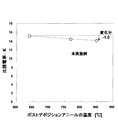
図2は、従来例におけるHfO2膜の堆積後のアニール処理(ポストデポジションアニール処理)の温度による比誘電率Kの変化を示す。なお、比誘電率Kは、界面層とHfO2層をともに含むゲート絶縁膜全体の平均値を示す。従来例の場合、HfO2膜は膜質が悪く、ポストデポジションアニール処理中で残留酸素が膜中を透過すると、Si基板が酸化されて比誘電率の低いSiO2層が形成される。その結果、ゲート絶縁膜全体の比誘電率Kは大きく減少する。従来例では、比誘電率Kの変化分(減少分)は5.5である。
【0020】
図3は、本発明におけるHfO2膜の堆積後のアニール処理(ポストデポジションアニール処理)の温度による比誘電率Kの変化を示す。本発明の場合、HfO2膜は膜質が良く、ポストデポジションアニール処理中で残留酸素が膜を透過することを防ぐことができる。その結果、ゲート絶縁膜全体の比誘電率Kの変化分(減少分)は上記従来例の場合よりも低減され、1.0に改善することができる。
【0021】
図4は、本発明及び従来例における、HfO2膜の膜厚によるゲートリーク電流密度の比較を示す。なお、HfO2膜の膜厚はエリプソメトリー法で測定し、ゲートリーク電流密度はゲート電極に−1Vの電圧を印加した時の絶縁膜に流れるリーク電流を測定した。本発明の場合、従来例と比較して、ゲートリーク電流密度が約4〜5桁程度も低減され、非常に大きな改善効果を示した。
【0022】
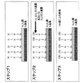
図5は、本発明による表面処理方法の概念図を示す。ステップ1でSi基板上にNH3ガス処理で極薄のシリコン窒化膜(Si3N4)を形成する。膜の最表面はSi−N−Hの結合で覆われている。その後、ステップ2でO2ガスとH2ガスの混合ガス、H2OガスまたはO2ガスを暴露し、膜の最表面の結合をSi−N−Hの結合からSi−N−OHの結合へ変化させる。この工程で、O2ガスとH2ガスの混合ガスを使用する場合は、ガス中の反応によりOH基が生成され、極薄のシリコン窒化膜(Si3N4)の表面を効果的に置換する。また、H2Oガスを使用する場合は、極薄のシリコン窒化膜(Si3N4)の表面でH2Oガスが分解し、生成されたOH基が効果的に表面を置換する。また、O2ガスを使用する場合は、極薄のシリコン窒化膜(Si3N4)の表面で存在するSi−N−Hの結合にO2ガスが反応し、Si−N−O−Hの結合に再配列され、効果的に表面を覆う。最終的には、ステップ3で示したように、膜の最表面をOH基で覆うようにする。
【0023】
この後、CVD処理で4nm程度の膜厚のHfO2膜を堆積する。この時、下地の極薄のシリコン窒化膜(Si3N4)の表面はOH基で覆われているので、該シリコン窒化膜(Si3N4)と上層のHfO2膜とが化学的に強固に結合し、かつ、HfO2膜も緻密で膜質良く成長する。その結果、図3で示したように酸素の突き抜けが抑制でき、かつ、図4で示したように電気特性としてゲートリーク電流が低い良質のゲート絶縁膜が形成できる。
【0024】
本実施形態によれば、Si基板の洗浄後にシリコン窒化膜の界面層を形成し、その後、O2ガスとH2ガスの混合ガス、H2OガスまたはO2ガスを上記シリコン窒化膜の表面に暴露し、その後、Hfを含有する高誘電率絶縁膜を堆積し、アニール処理を行う構成を設けることにより、緻密でかつゲートリーク電流の低い良質のHigh−Kゲート絶縁膜を形成することができる。
【0025】
なお、本実施形態でのSi基板上の極薄のシリコン窒化膜(Si3N4)は、拡散バリア性を有する高誘電率膜として、基板のシリコン(Si)が酸化される反応を防止している。Si基板の酸化層で、比誘電率がSiO2に近い界面層ができると、膜全体としての比誘電率Kが極端に下がってしまうため、Si基板の酸化を防止している。また、Si基板とHfO2膜との間の拡散防止層は、Nを含有するガス中での熱窒化およびプラズマ窒化などを形成方法としても挙げられる。また、HfO2蒸着形成の初期部分にNを含有するガスを導入し、直接Si基板側を窒素含有の高誘電体絶縁膜とする工程を設けても良い。また、High−K材料を蒸着する前に、Si基板側にSi3N4などの拡散防止膜を形成する時にも、この拡散防止膜にHなどを含有させることは効果的である。
【0026】
また、本実施形態において、Si基板上の極薄のシリコン窒化膜(Si3N4)表面にO2ガスとH2ガスの混合ガスまたはH2Oガスを暴露する代わりに、Si基板上に極薄のシリコンケミカル酸化膜(SiOx)または極薄のシリコン酸化膜(SiO2)またはシリコン酸窒化膜(SiOxNy)を形成し、その表面にO2ガスとH2ガスの混合ガス、H2Oガス、O2ガスまたはH2ガスを暴露することで、OH基の終端を行っても良い。
【0027】
また、本実施形態において、HfO2膜であるHigh−K膜の上層に第2の拡散バリア性を有する高誘電率膜を設置し、ゲート電極材料であるポリシリコンとハフニウムとが必要以上に反応することを防止し、比誘電率Kの低下を抑えることも可能である。第2の拡散バリア性を有する高誘電率膜は窒素を含むことにより、バリア効果を高めている。また、HfO2膜上の拡散防止膜は、窒素を含有するガス中での熱窒化やプラズマ窒化、または窒化シリコン層の堆積などで形成することができる。また、ゲート電極形成の初期に窒素ガスを導入し、HfO2の表面を窒化する方法なども有効である。また、HfO2蒸着形成の最終部分に窒素を含有するガスを導入し、表面側に窒素含有の高誘電体絶縁膜を形成しても良い。さらに、ゲート絶縁膜の膜全体や、膜のいずれかの部分に窒素を含有しても良い。
【0028】
また、本実施形態において、HfO2膜を用いて説明したが、これに代えてZrO2膜を用いても本発明の効果は得られる。また、HfO2膜中にSi、Al、Ta、TiまたはLaなどの酸化物を形成する元素を混入する場合も同様に実施可能である。すなわち、High−K膜は、堆積時の組成や材料に関わらず化学反応として一般化できるため、本発明の効果は、HfO2とZrO2に限定されず、TiO2、Ta2O5、La2O3、CeO2、Al2O3またはBSTなど、あるいはこれらの3元系酸化膜(例えば、HfxAlyO2)、あるいはこれらの酸化膜にSiを含有するシリケイト膜にも適応可能である。
【0029】
また、本実施形態において、HfO2膜の原料には液体Hfソース(C16H36HfO4)を用いたが、以下の原料を用いることもできる。CVD法で堆積する場合は、TDEAH(Tetrakis diethylamido hafnium、テトラキスジエチルアミドハフニウム、C16H40N4Hf)、TDMAH(Tetrakis dimethylamino hafnium、テトラキスジメチルアミノハフニウム、C8H24N4Hf)、Hf(MMP)4(Tetrakis 1−Methoxy−2−methyl−2−propoxy hafnium、テトラキス1メトキシ2メチル2プロポキシハフニウム、Hf[OC(CH3)2CH2OCH3]4)または固体ソース(例えばHf(NO3)4)などもある。また、Hf金属、HfCl4、Hf t−butoxide、Hf nitratoまたはTDEA−HfなどをHf原料とし、O2、H2O、NO、N2OまたはNH3などを置換ガス原料として、各々を交互に暴露するALD法を用いても同様に実施可能である。また、CVD法の堆積に代えて、プラズマCVD法またはJVD(Jet Vapor Deposition)法でも同様に実施可能である。さらに、酸素含有ガスとしてO2を用いたが、NO、N2O、H2OまたはO3などでも同様に実施可能である。
【0030】
また、本実施形態において、ゲート電極材料はポリシリコンに代えて、金属を用いても良い。例えば、高誘電率膜の表面を窒化処理した後、Al/TiN(積層)、Taまたは金属窒化物(TiNまたはTaN)を形成しても良い。なお、金属窒化物のゲート電極にSiまたはGeを混ぜても良い。さらに、Ti、SiGe、Ta、TaN、TaSixNy、Ru、RuO2、RuO、WN、Mo、MoO、MoNなどでも同様に実施可能である。
【0031】
【発明の効果】
以上のように本発明は、Si基板の洗浄後にシリコン窒化膜の界面層を形成し、その後、O2ガスとH2ガスの混合ガス、H2OガスまたはO2ガスを上記シリコン窒化膜の表面に暴露し、その後、Hfを含有する高誘電率絶縁膜を堆積し、アニール処理を行う構成を設けることにより、緻密でかつゲートリーク電流の低い良質のHigh−Kゲート絶縁膜を形成することができる。
【図面の簡単な説明】
【図1】本発明の第1の実施形態におけるプロセスフロー図
【図2】従来例における比誘電率とポストデポジションアニール温度依存性を示す図
【図3】本発明の第1の実施形態における比誘電率とポストデポジションアニール温度依存性を示す図
【図4】本発明の第1の実施形態における物理膜厚とゲートリーク電流密度の依存性を示す図
【図5】本発明の第1の実施形態における表面処理の概念図
【図6】従来例におけるプロセスフロー図[0001]
TECHNICAL FIELD OF THE INVENTION
The present invention relates to a silicon semiconductor device, and more particularly to a method for forming a high dielectric constant gate insulating film.
[0002]
[Prior art]
2. Description of the Related Art MOSFETs have been miniaturized along with recent technological developments for high integration and high speed in semiconductor devices. As the thickness of the gate insulating film is reduced with miniaturization, a problem such as an increase in gate leak current due to a tunnel current becomes apparent. In order to suppress this problem, a gate insulating film using a high dielectric constant material such as HfO 2 and ZrO 2 in the gate insulating film (hereinafter, referred to as High-K gate insulating film) by a thin SiO 2 equivalent thickness ( A method of increasing the physical film thickness while realizing (EOT) has been studied. The following is known as a conventional method for forming a High-K gate insulating film (see Non-Patent Document 1).
[0003]
Hereinafter, a conventional example will be described with reference to FIG. FIG. 6 is a process flow diagram of a conventional example. First, using an Si substrate, after performing standard RCA cleaning and cleaning with hydrofluoric acid, an interface layer of a silicon nitride film is formed by treatment with NH 3 gas at 700 ° C. for 10 seconds. Next, using the N 2 gas as a carrier gas for C 16 H 36 HfO 4, CVD of mixed with oxygen gas for 3 minutes at 500 ℃ (Chemical Vapor Deposition) processing, 4 nm a film thickness of about HfO 2 film Is deposited. As a heat treatment after the deposition, an annealing treatment (post-deposition annealing treatment) is performed in a temperature range of 700 ° C. to 900 ° C. for 30 seconds in N 2 gas. Next, amorphous silicon is deposited at 540 ° C. and doped at 900 ° C. using POCl 3 . Thereafter, the activation treatment of the dopant of the gate electrode is performed at 900 ° C. to 1000 ° C. for 30 seconds to 60 seconds. By obtaining such a process, an n-type MOSFET is formed.
[0004]
[Non-patent document 1]
S. J. Lee et al. , "High Quality CVD HfO 2 Gate Stack with Poly-Si Gate Electrode", International Electron Devices Meeting Technical Digest, 2000, p31.
[0005]
[Problems to be solved by the invention]
However, the above configuration has a problem that the gate leakage current is increased due to many defects in the film.
[0006]
The present invention has been made in view of the above problems, and provides a method for forming a High-K gate insulating film with few defects.
[0007]
[Means for Solving the Problems]
In order to solve the above problems, a method of forming a high dielectric constant gate insulating film according to the present invention comprises the steps of: (a) cleaning a silicon substrate; and forming a silicon nitride film, a silicon oxynitride film or a silicon oxide film on the silicon substrate. Forming an interface layer consisting of: (b) exposing a gas containing at least oxygen to the interface layer; and (c) depositing a high dielectric constant insulating film on the interface layer after the step (c). (D), a step (e) of performing an annealing process on the high dielectric constant insulating film, and a step (f) of forming a gate electrode on the high dielectric constant insulating film after the step (e). It is characterized by the following.
[0008]
With this structure, a high-quality high-K gate insulating film which is dense and has low gate leakage current can be formed.
[0009]
In the above method for forming a high dielectric constant gate insulating film, the gas containing oxygen is preferably a mixed gas of oxygen gas and hydrogen gas, water vapor gas, or oxygen gas.
[0010]
In the above method for forming a high dielectric constant gate insulating film, it is preferable that in the step (c), a hydroxyl group is formed on the surface of the interface layer by exposing a gas containing oxygen to the interface layer.
[0011]
In the above method for forming a high dielectric constant gate insulating film, the high dielectric constant film is preferably an oxide film of a metal forming the high dielectric constant film.
[0012]
In the above-described method for forming a high dielectric constant gate insulating film, it is preferable that the high dielectric constant film is a silicate film made of silicon and a metal forming the high dielectric constant film.
[0013]
In the above method for forming a high dielectric constant gate insulating film, the metal is preferably hafnium or zirconium.
[0014]
In the above method for forming a high dielectric constant gate insulating film, the high dielectric constant film preferably further contains nitrogen.
[0015]
In the above method for forming a high dielectric constant gate insulating film, the high dielectric constant film is preferably formed by a chemical vapor deposition method.
[0016]
BEST MODE FOR CARRYING OUT THE INVENTION
Hereinafter, embodiments of the present invention will be described with reference to the drawings.
[0017]
FIG. 1 is a process flow chart of a method for forming a high dielectric constant gate insulating film in the present embodiment. First, using an Si substrate, after performing standard RCA cleaning and cleaning with hydrofluoric acid, an interface layer of a silicon nitride film is formed by treatment with NH 3 gas at 700 ° C. for 10 seconds. Thereafter, a mixed gas of O 2 gas and H 2 gas, H 2 O gas or O 2 gas is exposed to the surface of the silicon nitride film. Next, an N 2 gas is used as a carrier gas of C 16 H 36 HfO 4 , mixed with an oxygen gas, and subjected to a CVD process at 500 ° C. for 3 minutes to deposit an HfO 2 film having a thickness of about 4 nm. As a heat treatment after the deposition, an annealing treatment (post-deposition annealing treatment) is performed in a temperature range of 700 ° C. to 900 ° C. for 30 seconds in N 2 gas.
[0018]
Next, amorphous silicon is deposited at 540 ° C. and doped at 900 ° C. using POCl 3 . Thereafter, the activation treatment of the dopant of the gate electrode is performed at 900 ° C. to 1000 ° C. for 30 seconds to 60 seconds. By obtaining such a process, an n-type MOSFET is formed.
[0019]
FIG. 2 shows a change in the relative dielectric constant K according to the temperature of the annealing process (post-deposition annealing process) after the deposition of the HfO 2 film in the conventional example. The relative dielectric constant K indicates an average value of the entire gate insulating film including both the interface layer and the HfO 2 layer. In the case of the conventional example, the quality of the HfO 2 film is poor, and when residual oxygen passes through the film during the post-deposition annealing, the Si substrate is oxidized to form a SiO 2 layer having a low relative dielectric constant. As a result, the relative dielectric constant K of the entire gate insulating film is greatly reduced. In the conventional example, the change (decrease) in the relative dielectric constant K is 5.5.
[0020]
FIG. 3 shows a change in the relative dielectric constant K depending on the temperature of the annealing (post-deposition annealing) after the deposition of the HfO 2 film in the present invention. In the case of the present invention, the HfO 2 film has good film quality and can prevent the residual oxygen from permeating the film during the post-deposition annealing process. As a result, the change (decrease) in the relative dielectric constant K of the entire gate insulating film is reduced as compared with the case of the conventional example, and can be improved to 1.0.
[0021]
FIG. 4 shows a comparison of the gate leak current density depending on the thickness of the HfO 2 film in the present invention and the conventional example. Note that the thickness of the HfO 2 film was measured by an ellipsometry method, and the gate leak current density was measured by a leak current flowing through the insulating film when a voltage of −1 V was applied to the gate electrode. In the case of the present invention, the gate leak current density was reduced by about 4 to 5 digits as compared with the conventional example, and a very large improvement effect was exhibited.
[0022]
FIG. 5 shows a conceptual diagram of the surface treatment method according to the present invention. In step 1, an ultra-thin silicon nitride film (Si 3 N 4 ) is formed on the Si substrate by NH 3 gas treatment. The outermost surface of the film is covered with Si—N—H bonds. Then, in
[0023]
Thereafter, an HfO 2 film having a thickness of about 4 nm is deposited by CVD. At this time, since the surface of the underlying ultra-thin silicon nitride film (Si 3 N 4 ) is covered with an OH group, the silicon nitride film (Si 3 N 4 ) and the upper HfO 2 film are chemically formed. The HfO 2 film is firmly bonded and the HfO 2 film grows densely and with good film quality. As a result, the penetration of oxygen can be suppressed as shown in FIG. 3, and a high-quality gate insulating film having a low gate leak current as an electrical characteristic can be formed as shown in FIG.
[0024]
According to the present embodiment, after cleaning the Si substrate, an interface layer of the silicon nitride film is formed, and thereafter, a mixed gas of O 2 gas and H 2 gas, H 2 O gas or O 2 gas is applied to the surface of the silicon nitride film. To form a high-quality high-K gate insulating film that is dense and has a low gate leakage current by providing a structure for depositing a high dielectric constant insulating film containing Hf and performing an annealing process. it can.
[0025]
Note that the ultra-thin silicon nitride film (Si 3 N 4 ) on the Si substrate in the present embodiment is a high dielectric constant film having a diffusion barrier property to prevent a reaction in which silicon (Si) of the substrate is oxidized. ing. If an interface layer having a relative dielectric constant close to that of SiO 2 is formed in the oxide layer of the Si substrate, the relative dielectric constant K of the film as a whole is extremely lowered, thereby preventing the oxidation of the Si substrate. The diffusion preventing layer between the Si substrate and the HfO 2 film may be formed by a method such as thermal nitriding or plasma nitriding in a gas containing N. Further, a process may be provided in which a gas containing N is introduced into an initial portion of HfO 2 vapor deposition and the Si substrate side is directly used as a nitrogen-containing high dielectric insulating film. In addition, when a diffusion prevention film such as Si 3 N 4 is formed on the Si substrate side before depositing the High-K material, it is effective to include H or the like in the diffusion prevention film.
[0026]
In the present embodiment, instead of exposing a mixed gas of O 2 gas and H 2 gas or H 2 O gas to the surface of an ultra-thin silicon nitride film (Si 3 N 4 ) on the Si substrate, An ultra-thin silicon chemical oxide film (SiOx) or an ultra-thin silicon oxide film (SiO 2 ) or a silicon oxynitride film (SiOxNy) is formed, and a mixed gas of O 2 gas and H 2 gas, H 2 O The OH group may be terminated by exposing the gas, O 2 gas, or H 2 gas.
[0027]
In this embodiment, a high-dielectric-constant film having a second diffusion barrier property is provided on the High-K film, which is an HfO 2 film, so that the gate electrode material, polysilicon and hafnium react more than necessary. Can be prevented, and a decrease in the relative dielectric constant K can be suppressed. The high dielectric constant film having the second diffusion barrier property contains nitrogen to enhance the barrier effect. Further, the diffusion prevention film on the HfO 2 film can be formed by thermal nitridation or plasma nitridation in a gas containing nitrogen, or deposition of a silicon nitride layer. Further, a method in which nitrogen gas is introduced at the initial stage of gate electrode formation and the surface of HfO 2 is nitrided is also effective. Alternatively, a nitrogen-containing gas may be introduced into the final portion of the HfO 2 vapor deposition to form a nitrogen-containing high dielectric insulating film on the surface side. Further, nitrogen may be contained in the entire gate insulating film or in any part of the film.
[0028]
In the present embodiment, the description has been made using the HfO 2 film. However, the effect of the present invention can be obtained by using a ZrO 2 film instead. Further, the case where an element forming an oxide such as Si, Al, Ta, Ti, or La is mixed into the HfO 2 film can be similarly performed. That is, since the High-K film can be generalized as a chemical reaction regardless of the composition or material at the time of deposition, the effect of the present invention is not limited to HfO 2 and ZrO 2 , and TiO 2 , Ta 2 O 5 , La The present invention is also applicable to 2 O 3 , CeO 2 , Al 2 O 3, BST, or the like, or a ternary oxide film (for example, HfxAlyO 2 ), or a silicate film containing Si in these oxide films.
[0029]
Further, in the present embodiment, a liquid Hf source (C 16 H 36 HfO 4 ) is used as a raw material for the HfO 2 film, but the following raw materials can be used. When depositing by CVD method, TDEAH (Tetrakis diethylamido hafnium, tetrakis diethylamide hafnium, C 16 H 40 N 4 Hf ), TDMAH (Tetrakis dimethylamino hafnium, tetrakis (dimethylamino) hafnium, C 8 H 24 N 4 Hf ), Hf (MMP ) 4 (Tetrakis 1-Methoxy-2-methyl-2-propoxy hafnium, tetrakis 1-methoxy-2-methyl-2-propoxyhafnium, Hf [OC (CH 3 ) 2 CH 2 OCH 3 ] 4 ) or a solid source (eg, Hf (NO 3) 4 ). Further, Hf metal, HfCl 4 , Hft-butoxide, Hf nitrato or TDEA-Hf, etc. are used as Hf raw materials, and O 2 , H 2 O, NO, N 2 O, NH 3, etc. are used as replacement gas raw materials, and each of them is alternated. The present invention can be similarly implemented by using the ALD method of exposing to water. Further, instead of the deposition by the CVD method, a plasma CVD method or a JVD (Jet Vapor Deposition) method can be similarly performed. Further, although O 2 was used as the oxygen-containing gas, NO, N 2 O, H 2 O, O 3 , or the like can be used in the same manner.
[0030]
In this embodiment, a metal may be used as the gate electrode material instead of polysilicon. For example, after nitriding the surface of the high dielectric constant film, Al / TiN (laminated), Ta, or metal nitride (TiN or TaN) may be formed. Note that Si or Ge may be mixed in the metal nitride gate electrode. Furthermore, Ti, SiGe, Ta, TaN , TaSixNy, Ru,
[0031]
【The invention's effect】
As described above, according to the present invention, an interface layer of a silicon nitride film is formed after cleaning a Si substrate, and then a mixed gas of O 2 gas and H 2 gas, H 2 O gas or O 2 gas is applied to the silicon nitride film. Forming a high-quality dense high-K gate insulating film having a low gate leakage current by exposing the surface and then depositing a high dielectric constant insulating film containing Hf and performing an annealing process. Can be.
[Brief description of the drawings]
FIG. 1 is a process flow diagram according to a first embodiment of the present invention. FIG. 2 is a diagram showing a relative dielectric constant and a post-deposition annealing temperature dependency in a conventional example. FIG. FIG. 4 is a diagram showing the dependency of the relative dielectric constant and the post-deposition annealing temperature. FIG. 4 is a diagram showing the dependency of the physical film thickness and the gate leak current density in the first embodiment of the present invention. FIG. 6 is a conceptual diagram of a surface treatment in the embodiment of the present invention.
Claims (8)
前記シリコン基板上にシリコン窒化膜、シリコン酸窒化膜またはシリコン酸化膜からなる界面層を形成する工程(b)と、
少なくとも酸素を含むガスを前記界面層に暴露する工程(c)と、
前記工程(c)の後に、前記界面層上に高誘電率絶縁膜を堆積する工程(d)と、
前記高誘電率絶縁膜に対してアニール処理を行う工程(e)と、
前記工程(e)の後に、前記高誘電率絶縁膜上にゲート電極を形成する工程(f)とを備えたことを特徴とする高誘電率ゲート絶縁膜の形成方法。Cleaning the silicon substrate (a);
(B) forming an interface layer made of a silicon nitride film, a silicon oxynitride film or a silicon oxide film on the silicon substrate;
(C) exposing a gas containing at least oxygen to the interface layer;
(D) depositing a high dielectric constant insulating film on the interface layer after the step (c);
(E) performing an annealing process on the high dielectric constant insulating film;
Forming a gate electrode on the high dielectric constant insulating film after the step (e); and (f) forming a gate electrode on the high dielectric constant insulating film.
Priority Applications (1)
| Application Number | Priority Date | Filing Date | Title |
|---|---|---|---|
| JP2003082424A JP2004289082A (en) | 2003-03-25 | 2003-03-25 | Method of forming high-dielectric-constant gate insulating film |
Applications Claiming Priority (1)
| Application Number | Priority Date | Filing Date | Title |
|---|---|---|---|
| JP2003082424A JP2004289082A (en) | 2003-03-25 | 2003-03-25 | Method of forming high-dielectric-constant gate insulating film |
Publications (1)
| Publication Number | Publication Date |
|---|---|
| JP2004289082A true JP2004289082A (en) | 2004-10-14 |
Family
ID=33295720
Family Applications (1)
| Application Number | Title | Priority Date | Filing Date |
|---|---|---|---|
| JP2003082424A Pending JP2004289082A (en) | 2003-03-25 | 2003-03-25 | Method of forming high-dielectric-constant gate insulating film |
Country Status (1)
| Country | Link |
|---|---|
| JP (1) | JP2004289082A (en) |
Cited By (3)
| Publication number | Priority date | Publication date | Assignee | Title |
|---|---|---|---|---|
| JP2006140374A (en) * | 2004-11-15 | 2006-06-01 | Fujitsu Ltd | Manufacturing method for semiconductor device |
| JP2009164424A (en) * | 2008-01-08 | 2009-07-23 | Toshiba Corp | Semiconductor device and manufacturing method therefor |
| CN106558488A (en) * | 2015-09-30 | 2017-04-05 | 台湾积体电路制造股份有限公司 | Semiconductor device and forming method thereof |
-
2003
- 2003-03-25 JP JP2003082424A patent/JP2004289082A/en active Pending
Cited By (6)
| Publication number | Priority date | Publication date | Assignee | Title |
|---|---|---|---|---|
| JP2006140374A (en) * | 2004-11-15 | 2006-06-01 | Fujitsu Ltd | Manufacturing method for semiconductor device |
| JP2009164424A (en) * | 2008-01-08 | 2009-07-23 | Toshiba Corp | Semiconductor device and manufacturing method therefor |
| US8030198B2 (en) | 2008-01-08 | 2011-10-04 | Kabushiki Kaisha Toshiba | Semiconductor device and manufacturing method thereof |
| CN106558488A (en) * | 2015-09-30 | 2017-04-05 | 台湾积体电路制造股份有限公司 | Semiconductor device and forming method thereof |
| US10181397B2 (en) * | 2015-09-30 | 2019-01-15 | Taiwan Semiconductor Manufacturing Company Limited | Semiconductor device and method for forming the same |
| US10879061B2 (en) | 2015-09-30 | 2020-12-29 | Taiwan Semiconductor Manufacturing Company Limited | Semiconductor device and method for forming the same |
Similar Documents
| Publication | Publication Date | Title |
|---|---|---|
| US8168547B2 (en) | Manufacturing method of semiconductor device | |
| JP4165076B2 (en) | Semiconductor device having high dielectric constant insulating film | |
| US7999334B2 (en) | Hafnium tantalum titanium oxide films | |
| US7563729B2 (en) | Method of forming a dielectric film | |
| US7655099B2 (en) | High-k dielectric film, method of forming the same and related semiconductor device | |
| US7396719B2 (en) | Method of forming high dielectric film using atomic layer deposition and method of manufacturing capacitor having the high dielectric film | |
| US8076249B2 (en) | Structures containing titanium silicon oxide | |
| US7510983B2 (en) | Iridium/zirconium oxide structure | |
| US8102013B2 (en) | Lanthanide doped TiOx films | |
| US7432548B2 (en) | Silicon lanthanide oxynitride films | |
| JP2003218108A (en) | CVD DEPOSITION OF M-SiO GATE DIELECTRIC | |
| Ahn | ALD of Amorphous Lanthanide Doped Tiox Films | |
| JP2006344837A (en) | Semiconductor apparatus and manufacturing method thereof | |
| JP2004289082A (en) | Method of forming high-dielectric-constant gate insulating film | |
| WO2006009025A1 (en) | Semiconductor device and semiconductor device manufacturing method | |
| WO2010140278A1 (en) | Semiconductor device and process for manufacture thereof | |
| JP4220991B2 (en) | Manufacturing method of semiconductor device | |
| KR20050061077A (en) | Method for forming dielectric layer in semiconductor device | |
| Ahn et al. | Lanthanide doped TiO x films | |
| Gutt et al. | ALD of advanced high-k and metal gate stacks for MOS devices | |
| KR20040058751A (en) | Capacitor with improved dielectric layer and oxidation resistant layer in semiconductor device and the method for fabricating thereof |