WO2010128679A1 - 封着材料層付きガラス部材とそれを用いた電子デバイスおよびその製造方法 - Google Patents
封着材料層付きガラス部材とそれを用いた電子デバイスおよびその製造方法 Download PDFInfo
- Publication number
- WO2010128679A1 WO2010128679A1 PCT/JP2010/057830 JP2010057830W WO2010128679A1 WO 2010128679 A1 WO2010128679 A1 WO 2010128679A1 JP 2010057830 W JP2010057830 W JP 2010057830W WO 2010128679 A1 WO2010128679 A1 WO 2010128679A1
- Authority
- WO
- WIPO (PCT)
- Prior art keywords
- sealing
- glass
- glass substrate
- material layer
- layer
- Prior art date
- Legal status (The legal status is an assumption and is not a legal conclusion. Google has not performed a legal analysis and makes no representation as to the accuracy of the status listed.)
- Ceased
Links
Images




Classifications
-
- H—ELECTRICITY
- H10—SEMICONDUCTOR DEVICES; ELECTRIC SOLID-STATE DEVICES NOT OTHERWISE PROVIDED FOR
- H10F—INORGANIC SEMICONDUCTOR DEVICES SENSITIVE TO INFRARED RADIATION, LIGHT, ELECTROMAGNETIC RADIATION OF SHORTER WAVELENGTH OR CORPUSCULAR RADIATION
- H10F77/00—Constructional details of devices covered by this subclass
- H10F77/30—Coatings
- H10F77/306—Coatings for devices having potential barriers
- H10F77/311—Coatings for devices having potential barriers for photovoltaic cells
-
- C—CHEMISTRY; METALLURGY
- C03—GLASS; MINERAL OR SLAG WOOL
- C03C—CHEMICAL COMPOSITION OF GLASSES, GLAZES OR VITREOUS ENAMELS; SURFACE TREATMENT OF GLASS; SURFACE TREATMENT OF FIBRES OR FILAMENTS MADE FROM GLASS, MINERALS OR SLAGS; JOINING GLASS TO GLASS OR OTHER MATERIALS
- C03C27/00—Joining pieces of glass to pieces of other inorganic material; Joining glass to glass other than by fusing
- C03C27/06—Joining glass to glass by processes other than fusing
-
- C—CHEMISTRY; METALLURGY
- C03—GLASS; MINERAL OR SLAG WOOL
- C03C—CHEMICAL COMPOSITION OF GLASSES, GLAZES OR VITREOUS ENAMELS; SURFACE TREATMENT OF GLASS; SURFACE TREATMENT OF FIBRES OR FILAMENTS MADE FROM GLASS, MINERALS OR SLAGS; JOINING GLASS TO GLASS OR OTHER MATERIALS
- C03C8/00—Enamels; Glazes; Fusion seal compositions being frit compositions having non-frit additions
- C03C8/24—Fusion seal compositions being frit compositions having non-frit additions, i.e. for use as seals between dissimilar materials, e.g. glass and metal; Glass solders
-
- H—ELECTRICITY
- H01—ELECTRIC ELEMENTS
- H01J—ELECTRIC DISCHARGE TUBES OR DISCHARGE LAMPS
- H01J17/00—Gas-filled discharge tubes with solid cathode
- H01J17/02—Details
- H01J17/18—Seals between parts of vessels; Seals for leading-in conductors; Leading-in conductors
- H01J17/183—Seals between parts of vessel
-
- H—ELECTRICITY
- H01—ELECTRIC ELEMENTS
- H01J—ELECTRIC DISCHARGE TUBES OR DISCHARGE LAMPS
- H01J5/00—Details relating to vessels or to leading-in conductors common to two or more basic types of discharge tubes or lamps
- H01J5/20—Seals between parts of vessels
- H01J5/22—Vacuum-tight joints between parts of vessel
- H01J5/24—Vacuum-tight joints between parts of vessel between insulating parts of vessel
-
- H—ELECTRICITY
- H01—ELECTRIC ELEMENTS
- H01J—ELECTRIC DISCHARGE TUBES OR DISCHARGE LAMPS
- H01J9/00—Apparatus or processes specially adapted for the manufacture, installation, removal, maintenance of electric discharge tubes, discharge lamps, or parts thereof; Recovery of material from discharge tubes or lamps
- H01J9/24—Manufacture or joining of vessels, leading-in conductors or bases
- H01J9/26—Sealing together parts of vessels
-
- H—ELECTRICITY
- H01—ELECTRIC ELEMENTS
- H01J—ELECTRIC DISCHARGE TUBES OR DISCHARGE LAMPS
- H01J9/00—Apparatus or processes specially adapted for the manufacture, installation, removal, maintenance of electric discharge tubes, discharge lamps, or parts thereof; Recovery of material from discharge tubes or lamps
- H01J9/24—Manufacture or joining of vessels, leading-in conductors or bases
- H01J9/26—Sealing together parts of vessels
- H01J9/261—Sealing together parts of vessels the vessel being for a flat panel display
-
- H—ELECTRICITY
- H10—SEMICONDUCTOR DEVICES; ELECTRIC SOLID-STATE DEVICES NOT OTHERWISE PROVIDED FOR
- H10F—INORGANIC SEMICONDUCTOR DEVICES SENSITIVE TO INFRARED RADIATION, LIGHT, ELECTROMAGNETIC RADIATION OF SHORTER WAVELENGTH OR CORPUSCULAR RADIATION
- H10F19/00—Integrated devices, or assemblies of multiple devices, comprising at least one photovoltaic cell covered by group H10F10/00, e.g. photovoltaic modules
- H10F19/80—Encapsulations or containers for integrated devices, or assemblies of multiple devices, having photovoltaic cells
- H10F19/807—Double-glass encapsulation, e.g. photovoltaic cells arranged between front and rear glass sheets
-
- H—ELECTRICITY
- H10—SEMICONDUCTOR DEVICES; ELECTRIC SOLID-STATE DEVICES NOT OTHERWISE PROVIDED FOR
- H10K—ORGANIC ELECTRIC SOLID-STATE DEVICES
- H10K59/00—Integrated devices, or assemblies of multiple devices, comprising at least one organic light-emitting element covered by group H10K50/00
- H10K59/80—Constructional details
- H10K59/87—Passivation; Containers; Encapsulations
- H10K59/871—Self-supporting sealing arrangements
- H10K59/8722—Peripheral sealing arrangements, e.g. adhesives, sealants
-
- H—ELECTRICITY
- H01—ELECTRIC ELEMENTS
- H01J—ELECTRIC DISCHARGE TUBES OR DISCHARGE LAMPS
- H01J2329/00—Electron emission display panels, e.g. field emission display panels
- H01J2329/86—Vessels
- H01J2329/867—Seals between parts of vessels
-
- Y—GENERAL TAGGING OF NEW TECHNOLOGICAL DEVELOPMENTS; GENERAL TAGGING OF CROSS-SECTIONAL TECHNOLOGIES SPANNING OVER SEVERAL SECTIONS OF THE IPC; TECHNICAL SUBJECTS COVERED BY FORMER USPC CROSS-REFERENCE ART COLLECTIONS [XRACs] AND DIGESTS
- Y02—TECHNOLOGIES OR APPLICATIONS FOR MITIGATION OR ADAPTATION AGAINST CLIMATE CHANGE
- Y02E—REDUCTION OF GREENHOUSE GAS [GHG] EMISSIONS, RELATED TO ENERGY GENERATION, TRANSMISSION OR DISTRIBUTION
- Y02E10/00—Energy generation through renewable energy sources
- Y02E10/50—Photovoltaic [PV] energy
Definitions
- the present invention relates to a glass member with a sealing material layer, an electronic device using the same, and a method for producing the same.
- Flat-type display devices such as organic EL displays (Organic Electro-Luminescence Display: OELD), plasma display panels (PDP), liquid crystal display devices (LCD), etc. are glass substrates for elements on which display elements such as light emitting elements are formed. And a glass substrate for sealing are arranged opposite to each other, and the display element is sealed with a glass package in which these two glass substrates are sealed (see Patent Document 1). Furthermore, in solar cells such as dye-sensitized solar cells, it has been studied to apply a glass package in which solar cell elements are sealed with two glass substrates (see Patent Document 2).
- sealing resin or sealing glass As a sealing material for sealing between two glass substrates, sealing resin or sealing glass is used. Since organic EL (OEL) elements and the like are easily deteriorated by moisture, application of sealing glass excellent in moisture resistance and the like is being promoted. Since the sealing temperature with the sealing glass is about 400 to 600 ° C., the characteristics of the electronic element part such as the OEL element deteriorate when heat treatment is performed using a baking furnace. Therefore, a sealing glass material layer including a laser absorbing material is disposed between the sealing regions provided in the peripheral portions of the two glass substrates, and the sealing glass material layer is locally irradiated by irradiating the laser beam thereto. Attempts have been made to seal by heating and melting (see Patent Documents 1 and 2).
- Laser sealing can suppress the thermal effect on the electronic element part, but on the other hand, the glass substrate is cracked or cracked at the time of sealing, and the wiring layer (on the surface of the glass substrate ( The conductive film) has a drawback that peeling easily occurs.
- laser sealing first, a sealing glass material containing a laser absorbing material is baked on the sealing region of the sealing glass substrate to form a frame-shaped sealing glass material layer. Next, after laminating the sealing glass substrate and the element glass substrate via the sealing glass material layer, the sealing glass material layer is heated and melted by irradiating laser light from the sealing glass substrate side. To seal between the glass substrates.
- Laser light is irradiated while scanning along the frame-shaped sealing glass material layer.
- the glass material layer for sealing is melted by locally heating the irradiated portion of the laser beam, and is rapidly cooled and solidified from the time when the irradiation of the laser beam is completed. At this time, the glass material layer for sealing melts and solidifies with a film thickness reduction of about 30 to 50%. Since the reduction in the film thickness of the sealing glass material layer occurs locally continuously in the irradiated portion of the laser beam, it acts as a peeling force on the wiring layer formed on the surface of the glass substrate. As a result, problems such as peeling of the wiring layer and the accompanying deterioration in airtightness occur. Furthermore, stress based on the reduced film thickness of the glass material layer for sealing is applied to the glass substrate. Since this stress is abruptly applied to the local portion, the glass substrate is likely to be cracked or broken.
- the object of the present invention is to suppress the occurrence of defects such as cracks and cracks in the glass substrate when applying local heating to the sealing between the two glass substrates, thereby sealing the glass substrate and its reliability.
- the glass member with a sealing material layer that can enhance the property, the method for producing the glass member with the sealing material layer, and further the use of such a glass member with the sealing material layer enables airtightness and its reliability. It is an object of the present invention to provide an electronic device and a method for manufacturing the same.
- a glass member with a sealing material layer according to an aspect of the present invention is provided on a glass substrate having a sealing region, and the sealing region of the glass substrate, and includes a sealing glass, a low expansion filler, and an electromagnetic wave absorber.
- a sealing material layer comprising a fired layer of a glass material for sealing containing, wherein the sealing material layer contains air bubbles in a volume ratio of 10 to 30%, and a mass ratio of 50 to 200 ppm. It is characterized by containing a range of carbon.
- the method for producing a glass member with a sealing material layer according to an aspect of the present invention includes a sealing glass, a low expansion filler, and an electromagnetic wave absorbing material on the sealing region of a glass substrate having a sealing region. Forming a wearing glass material layer, and then firing the sealing glass material layer to contain air bubbles in a range of 10 to 30% by volume and containing carbon in a range of 50 to 200 ppm by mass It is characterized by a material layer.
- An electronic device includes a first glass substrate having an element formation region including an electronic element, and a first sealing region provided on an outer peripheral side of the element formation region, and the first glass substrate
- the glass substrate has a second sealing region corresponding to the first sealing region, and the surface having the second sealing region has the first sealing region of the first glass substrate.
- the first sealing region and the second glass substrate are disposed so as to face the surface, and the space between the first glass substrate and the second glass substrate is sealed.
- An electronic device manufacturing method provides a first glass substrate having an element formation region including an electronic element and a first sealing region provided on an outer peripheral side of the element formation region.
- a second sealing region corresponding to the first sealing region of the first glass substrate, a sealing glass, a low expansion filler, and an electromagnetic wave absorbing material formed on the second sealing region.
- a sealing material layer containing carbon in the range of 50 to 200 ppm by mass and containing bubbles in the range of 10 to 30% by volume.
- a second glass substrate is prepared, and the first glass substrate and the second glass substrate are opposed to each other with a surface having the first sealing region and a surface having the second sealing region.
- the sealing material layer is irradiated with electromagnetic waves through the first glass substrate or the second glass substrate and locally heated to grow at least a part of the bubbles in the sealing material layer, while the sealing material layer is grown.
- the sealing material layer is melted to form a sealing layer that seals between the first glass substrate and the second glass substrate.
- the glass member with a sealing material layer and the manufacturing method thereof according to the aspect of the present invention it is possible to suppress defects such as cracks and cracks of the glass substrate at the time of sealing using local heating with high reproducibility. Therefore, according to the electronic device and the manufacturing method thereof according to the aspect of the present invention, it is possible to improve the airtightness and the reliability thereof.
- FIG. 1 is a diagram showing a configuration of an electronic device according to an embodiment of the present invention
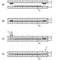
- FIG. 2 is a diagram showing a manufacturing process of the electronic device
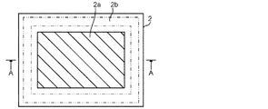
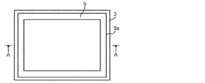
- FIGS. 3 to 6 are diagrams showing configurations of first and second glass substrates used therefor.
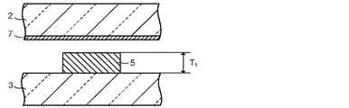
- FIG. 7 is an enlarged sectional view showing a part of the first and second glass substrates
- FIG. 8 is an enlarged sectional view showing a part of the electronic device.
- An electronic device 1 shown in FIG. 1 constitutes a lighting device using a light emitting element such as an FPD such as an OELD, PDP, or LCD, or an OEL element, or a solar cell such as a dye-sensitized solar cell.
- a light emitting element such as an FPD such as an OELD, PDP, or LCD, or an OEL element
- a solar cell such as a dye-sensitized solar cell.
- the electronic device 1 includes a first glass substrate (element glass substrate) 2 having an element formation region 2 a including an electronic element, and a second glass substrate (sealing glass substrate) 3.
- the first and second glass substrates 2 and 3 are made of, for example, non-alkali glass or soda lime glass.
- the alkali-free glass has a thermal expansion coefficient of about 35 to 40 ( ⁇ 10 ⁇ 7 / ° C.).
- Soda lime glass has a thermal expansion coefficient of about 85 to 90 ( ⁇ 10 ⁇ 7 / ° C.).
- an electronic element corresponding to the electronic device 1 for example, an OEL element for OELD or OEL illumination, a plasma light emitting element for PDP, a liquid crystal display element for LCD, If it is a solar cell, a dye-sensitized photoelectric conversion part etc. will be formed.
- Electronic elements such as light emitting elements such as OEL elements and solar cell elements such as dye-sensitized photoelectric conversion units have various known structures, and are not limited to these element structures.
- the first glass substrate 2 has a first sealing region 2b provided on the outer peripheral side of the element formation region 2a.
- the first sealing region 2b is set so as to surround the element formation region 2a.
- the second glass substrate 3 has a second sealing region 3a.
- the second sealing region 3a corresponds to the first sealing region 2b. That is, when the first glass substrate 2 and the second glass substrate 3 are disposed to face each other, the first sealing region 2b and the second sealing region 3a are set to face each other, which will be described later. Thus, it becomes the formation region of the sealing layer 4 (the formation region of the sealing material layer 5 for the second glass substrate 3).
- the first glass substrate 2 and the second glass substrate 3 are arranged so that the surfaces having the sealing regions 2b and 3a are opposed to each other and, for example, a gap is formed on the element formation region 2a. In a solar cell element or the like, a gap may not be formed on the element formation region 2a.
- the space between the first glass substrate 2 and the second glass substrate 3 is sealed with a sealing layer 4. That is, the sealing layer 4 seals between the sealing region 2 b of the first glass substrate 2 and the sealing region 3 a of the second glass substrate 3 while providing a gap between the glass substrates 2 and 3. Is formed.
- the electronic element formed in the element formation region 2 a is hermetically sealed with a glass panel constituted by the first glass substrate 2, the second glass substrate 3, and the sealing layer 4.
- the sealing layer 4 is composed of a melt-fixed layer in which the sealing material layer 5 formed on the sealing region 3 a of the second glass substrate 3 is melted and fixed to the sealing region 2 b of the first glass substrate 2. Is.
- the sealing material layer 5 is melted by local heating using an electromagnetic wave 6 such as laser light or infrared light. That is, the frame-shaped sealing material layer 5 is formed in the sealing region 3a of the second glass substrate 3 used for manufacturing the electronic device 1 as shown in FIGS.
- electromagnetic waves 6 such as laser light and infrared rays.
- the 1st glass substrate 2 has the thin film 7 formed in the surface which has the sealing area
- the thin film 7 formed on the surface of the first glass substrate 2 functions, for example, as a wiring for drawing out the electrode of the electronic element formed in the element forming region 2a to the outside of the glass panel.
- Typical examples of the thin film 7 functioning as a wiring include a transparent conductive film such as a tin-doped indium oxide (ITO) film or a fluorine-doped tin oxide (FTO) film.
- the transparent conductive film such as the ITO film or the FTO film is not limited to the single film, and may be laminated with another conductive film or an insulating film.
- the conductive film laminated with the ITO film or the FTO film include conductive metal films such as an aluminum film, an aluminum alloy film, a copper film, and a copper alloy film.
- the insulating film include insulating inorganic compound films such as a silicon oxide film and a silicon nitride film.
- the thin film 7 may be composed of only a conductive metal film, an insulating inorganic compound film, or a laminated film thereof.
- the thin film 7 is made of at least one selected from a conductive film and an insulating film.
- a thin film is also formed on the surface of the second glass substrate 3 having the sealing region 3a.
- a thin film may be formed only on the surface of the second glass substrate 3 having the sealing region 3a.
- FIG. 7 shows the thin film 7 formed on the surface having the sealing region 2b of the first glass substrate 2, but the form of the thin film 7 is not limited to this.
- the second glass substrate 2 or 3 is formed on the surface having at least one sealing region 2b or 3a.
- the thin film 7 When the thin film 7 is formed on the surface of the first glass substrate 2 as a wiring for drawing out the electrode of the electronic element to the outside of the glass panel, the thin film 7 is formed so as to cross the sealing region 2b. Therefore, as shown in FIG. 8, at least a part of the sealing layer 4 comes into contact with the thin film 7.
- a thin film is formed on the surface of the second glass substrate 3, and at least a part of the sealing material layer 5 and thus the sealing layer 4 is in contact with the thin film.
- the sealing material layer 5 is a fired layer of a sealing glass material containing a sealing glass (glass frit), an electromagnetic wave absorbing material (a material that generates heat by absorbing electromagnetic waves such as laser light and infrared rays), and a low expansion filler. is there.
- the glass material for sealing preferably contains a low expansion filler in order to match the coefficient of thermal expansion with the coefficient of thermal expansion of the glass substrates 2 and 3.
- the glass material for sealing is obtained by blending an electromagnetic wave absorbing material and a low expansion filler into sealing glass as a main component.
- the glass material for sealing may contain additives other than these as required.
- sealing glass for example, low-melting glass such as tin-phosphate glass, bismuth glass, vanadium glass, lead glass or the like is used.
- tin-phosphate glass is used in consideration of sealing properties (adhesiveness) to glass substrates 2 and 3, reliability thereof (adhesion reliability and sealing properties), and influence on the environment and human body.
- sealing glass made of bismuth glass is preferable to use.
- the glass transition point of the sealing glass is preferably 250 to 300 ° C. From this point, it is desirable to use tin-phosphate glass.
- Tin-phosphate glass is composed of 20 to 68 mol% SnO, 0.5 to 5 mol% SnO 2 and 20 to 40 mol% P 2 O 5 (basically a total amount of 100%). It is preferable to have a composition of (mol%). SnO is a component for lowering the melting point of glass. If the SnO content is less than 20 mol%, the viscosity of the glass becomes high and the sealing temperature becomes too high, and if it exceeds 68 mol%, it will not vitrify.
- SnO 2 is a component for stabilizing the glass.
- SnO 2 is a component for stabilizing the glass.
- SnO 2 is separated and precipitated in the glass that has been softened and melted during the sealing operation, the fluidity is impaired, and the sealing workability is lowered.
- SnO 2 exceeds 5 mol%, SnO 2 is likely to precipitate during melting of the low-melting glass.
- P 2 O 5 is a component for forming a glass skeleton.
- the content of P 2 O 5 is less than 20 mol%, the glass does not vitrify, and when the content exceeds 40 mol%, the weather resistance, which is a disadvantage specific to phosphate glass, may be deteriorated.
- the ratio (mol%) of SnO and SnO 2 in the glass frit can be determined as follows. First, after the glass frit (low melting point glass powder) is acid-decomposed, the total amount of Sn atoms contained in the glass frit is measured by ICP emission spectroscopic analysis. Next, since Sn 2+ (SnO) is obtained by acidimetric decomposition, the amount of Sn 2+ determined there is subtracted from the total amount of Sn atoms to obtain Sn 4+ (SnO 2 ).
- the glass formed of the above three components has a low glass transition point and is suitable for a low-temperature sealing material.
- a component that forms a glass skeleton such as SiO 2 , ZnO, B 2 O 3 , Al 2 O 3, WO 3, MoO 3, Nb 2 O 5, TiO 2, ZrO 2, Li 2 O, stabilizing Na 2 O, K 2 O, Cs 2 O, MgO, CaO, SrO, the glass BaO, etc.
- the component to be made may be contained as an optional component. However, if the content of any component is too large, the glass becomes unstable and devitrification may occur, and the glass transition point and softening point may increase. Therefore, the total content of any component is 30 mol%. The following is preferable.
- the glass composition in this case is adjusted so that the total amount of the basic component and the optional component is basically 100 mol%.
- the glass material for sealing contains an electromagnetic wave absorber that functions as a laser absorber or an infrared absorber.
- an electromagnetic wave absorbing material a compound such as at least one metal selected from Fe, Cr, Mn, Co, Ni and Cu or an oxide containing the metal is used.
- the content of the electromagnetic wave absorbing material is preferably in the range of 0.1 to 10% by volume with respect to the sealing glass material. When the content of the electromagnetic wave absorbing material is less than 0.1% by volume, the sealing material layer 5 cannot be sufficiently melted when irradiated with laser light or infrared rays.
- the second glass substrate 3 may be cracked due to local heat generation near the interface with the second glass substrate 3 when irradiated with laser light or infrared rays. Moreover, there is a possibility that the fluidity at the time of melting of the glass material for sealing deteriorates and the adhesiveness with the first glass substrate 2 is lowered.
- the glass material for sealing further contains a low expansion filler.
- a low expansion filler at least one selected from silica, alumina, zirconia, zirconium silicate, cordierite, zirconium phosphate compound, soda lime glass and borosilicate glass is used.
- Zirconium phosphate compounds include (ZrO) 2 P 2 O 7 , NaZr 2 (PO 4 ) 3 , KZr 2 (PO 4 ) 3 , Ca 0.5 Zr 2 (PO 4 ) 3 , Na 0.5 Nb.
- the low expansion filler has a lower thermal expansion coefficient than the sealing glass which is the main component of the sealing glass material.
- the content of the low expansion filler is appropriately set so that the thermal expansion coefficient of the sealing glass material approaches the thermal expansion coefficient of the glass substrates 2 and 3.
- the low expansion filler is preferably contained in the range of 1 to 50% by volume with respect to the sealing glass material, although it depends on the thermal expansion coefficient of the sealing glass and the glass substrates 2 and 3. If the content of the low expansion filler is less than 1% by volume, the effect of adjusting the thermal expansion coefficient of the glass material for sealing cannot be sufficiently obtained. On the other hand, if the content of the low expansion filler exceeds 50% by volume, the fluidity of the glass material for sealing may be lowered and the adhesive strength may be lowered.
- the content of the low expansion filler is desirably in the range of 25 to 50% by volume.
- swelling filler into 25 volume% or more, the fluidity
- the content of the low expansion filler is too large, the fluidity of the glass material for sealing is too low, so the content of the low expansion filler is preferably 50% by volume or less.
- the thermal expansion coefficient of the sealing glass material containing the sealing glass, the low expansion filler and the electromagnetic wave absorbing material is preferably 40 to 85 ( ⁇ 10 ⁇ 7 / ° C.), and 45 to 75 ( ⁇ 10 ⁇ 7 / ° C.). ) Is more preferable.
- the sealing material layer 5 when using, for example, laser light for local heating of the sealing material layer 5, the sealing material layer 5 is melted in order from the portion irradiated with the laser light scanned along the laser beam, and rapidly cooled with the end of the laser light irradiation. It is solidified and fixed to the first glass substrate 2. Thus, melting and solidification of the sealing material layer 5 occurs locally and continuously. For this reason, if the film thickness reduction of the sealing material layer 5 at the time of melting is large, a force is applied to the thin film 7 formed on the surface of the glass substrate 2 (3) in the peeling direction. Further, stress based on the reduced film thickness of the sealing material layer 5 is applied to the glass substrates 2 and 3. Since this stress is abruptly applied to the local portion, the glass substrates 2 and 3 are cracked or broken.
- the sealing material layer 5 of the embodiment contains 10 to 30% of bubbles by volume. It is considered that the minute bubbles existing in the sealing material layer 5 expand when heated by laser irradiation, infrared irradiation, or the like, or bubbles adjacent to each other grow together.
- carbon is vaporized as carbon dioxide gas, which may increase the amount of gas or generate new bubbles.
- the ratio of the bubbles in the sealing material layer 5 is less than 10% by volume, it is not possible to sufficiently obtain the effect of suppressing the film thickness reduction based on the volume expansion of the bubbles when irradiated with laser light or infrared rays.
- the bubbles are less than 10% by volume, the volume expansion that compensates for the film thickness decrease due to the melt flow of the sealing material layer 5, that is, the effect of increasing the film thickness cannot be obtained sufficiently.
- the ratio of the bubbles in the sealing material layer 5 exceeds 30% by volume, the adhesive strength of the sealing layer 4 is lowered by excessively increasing the volume of the bubbles after melting and solidification.
- the size of the bubbles in the sealing material layer 5 is preferably in the range of 0.1 to 50 ⁇ m.
- the size of the bubble indicates the major axis. If the size of the bubbles is smaller than 0.1 ⁇ m, when the amount of bubbles is increased, the dispersed state of the bubbles becomes too dense, and the thickness of the glass layer between the bubbles may be reduced. In such a state, the adhesive strength of the sealing layer 4 tends to decrease. On the other hand, if the size of the bubble exceeds 50 ⁇ m, it becomes easy to form an open cell after irradiation with laser light or infrared rays, and the hermeticity of the sealing layer 4 may be lowered.
- the sealing material layer 5 contains an appropriate amount of carbon. Carbon reacts with oxygen in the glass component during heating to become a gas such as carbon dioxide. In this way, by generating gas in the sealing material layer 5 during heating, bubbles can be grown more effectively. In order to obtain such an effect, the amount of carbon in the sealing material layer 5 is in the range of 50 to 200 ppm by mass.
- the amount of carbon in the sealing material layer 5 exceeds 200 ppm, the amount of gas generated during laser heating or infrared heating will increase so much that open cells may increase and the hermeticity of the sealing layer 4 may decrease. is there. If the amount of carbon in the sealing material layer 5 is less than 50 ppm, the amount of generated gas is insufficient, and the volume of bubbles in the sealing material layer 5 cannot be increased sufficiently. In this case, the difference in film thickness between the part that has been heated and solidified and the part that has been heated and melted increases, and strains based on such film thickness difference accumulate, thereby cracking the glass substrates 2 and 3. Further, cracking or peeling of the sealing layer 4 and peeling of the thin film 7 are likely to occur.
- the volume ratio of the bubbles is preferably in the range of 5 to 35%.
- the volume ratio is preferably larger than the volume ratio of bubbles in the sealing material layer 5 before sealing.
- the size (major axis) of the bubbles in the sealing layer 4 is preferably in the range of 0.1 to 100 ⁇ m.
- bubbles larger than the bubbles in the sealing material layer 5 before sealing exist. That the bubble ratio of the sealing layer 4 is small and the size of the bubbles is small means that the film thickness reduction from the sealing material layer 5 is not sufficiently suppressed.
- the glass substrates 2 and 3 are cracked, the sealing layer 4 is cracked and peeled off, and the thin film 7 is peeled off.
- the ratio of the bubbles in the sealing layer 4 is large and the size of the bubbles is large, the adhesive strength and airtightness of the sealing layer 4 are likely to be lowered.
- the thickness T 2 of the sealing layer 4, the thickness T 1 of the sealing material layer 5 is preferably set to 0.9 T 1 or 1.1 T 1 or less. Furthermore, the volume V 2 of the sealing layer 4 is preferably in the range of more than 1V 1 and 1.15 V 1 or less with respect to the volume V 1 of the sealing material layer 5. By satisfying such conditions, reproducibility of cracking of the glass substrates 2 and 3, cracking and peeling of the sealing layer 4, peeling of the thin film 7, and the like due to a decrease in film thickness when the sealing material layer 5 is melted. It becomes possible to suppress well.
- the thickness T 2 of the sealing layer 4 and even more preferably to a 1T 1 or more. More preferably, the volume V 2 of the sealing layer 4 is 1.02 V 1 or more.
- the sealing material layer 5 is formed on the sealing region 3a of the second glass substrate 3 as follows.
- a sealing material paste is prepared by mixing a sealing glass material with a vehicle.
- the vehicle is obtained by dissolving a resin as a binder component in a solvent.
- the resin for the vehicle include cellulose resins such as methyl cellulose, ethyl cellulose, carboxymethyl cellulose, oxyethyl cellulose, benzyl cellulose, propyl cellulose, nitrocellulose, methyl methacrylate, ethyl methacrylate, butyl methacrylate, 2-hydroxyethyl methacrylate, butyl acrylate.
- Organic resins such as acrylic resins obtained by polymerizing one or more acrylic monomers such as 2-hydroxyethyl acrylate are used.
- Solvents such as terpineol, butyl carbitol acetate, and ethyl carbitol acetate are used in the case of a cellulose resin, and solvents such as methyl ethyl ketone, terpineol, butyl carbitol acetate, and ethyl carbitol acetate are used in the case of an acrylic resin. .
- the viscosity of the sealing material paste may be adjusted to the viscosity corresponding to the apparatus applied to the glass substrate 3, and can be adjusted by the ratio of the resin (binder component) and the solvent in the vehicle and the ratio of the sealing glass material and the vehicle.
- a known additive may be added to the sealing material paste as a glass paste such as an antifoaming agent or a dispersing agent.
- a known method using a rotary mixer equipped with a stirring blade, a roll mill, a ball mill or the like can be applied to the preparation of the sealing material paste.
- the sealing material paste is applied to the sealing region 3a of the second glass substrate 3 and dried to form an application layer of the sealing material paste.
- the sealing material paste is applied onto the second sealing region 3a by applying a printing method such as screen printing or gravure printing, or is applied along the second sealing region 3a using a dispenser or the like. To do.
- the coating layer of the sealing material paste is dried, for example, at a temperature of 120 ° C. or more for 10 minutes or more. A drying process is implemented in order to remove the solvent in an application layer. If the solvent remains in the coating layer, the binder component may not be sufficiently decomposed and burned in the subsequent firing step.
- the sealing material layer 5 is formed by baking the coating layer of the sealing material paste described above.
- the coating layer is first heated to a temperature below the glass transition point of sealing glass (glass frit), which is the main component of the sealing glass material, the binder component in the coating layer is decomposed and burned, and then sealed. Heated to a temperature equal to or higher than the softening point of glass (glass frit), melting glass material for sealing, foaming and foaming the melt with gas generated by decomposition and combustion of binder components (hereinafter referred to as decomposition gas)
- decomposition gas gas generated by decomposition and combustion of binder components
- the sealing material layer 5 when the binder component is decomposed and burned by heating to a temperature below the glass transition point of the sealing glass, it is heated to a temperature above the softening point of the sealing glass.
- the amount of bubbles and the size of the bubbles in the sealing material layer 5 can be controlled by adjusting the temperature rising rate and the like.
- the decomposition gas is removed at a heating rate of 1 to 10 ° C./min from the softening point of the sealing glass to the firing temperature.
- the rate of temperature rise in the range of 20 to 70 ° C./min, it is possible to obtain the sealing material layer 5 in which the cracked gas remains and in which bubbles of an appropriate size are present in the desired range.
- the heating rate is increased within this range, the amount of bubbles increases and small bubbles are obtained, and if the rate of increase is slow, the amount of bubbles decreases and large bubbles are obtained.
- the step of forming the sealing material layer 5 (1) an organic substance or carbon is added to the sealing glass (or sealing glass material) as a carbon source, and the carbon derived from the carbon source is contained in the sealing glass material.
- the method (2) is preferable because the amount of carbon can be controlled without adding a special step. It should be noted that methods other than these can be applied as long as the carbon content of the sealing material layer 5 can be within a range of 50 to 200 ppm by mass.
- an organic substance such as alcohol is added as a carbon source when the glass is crushed.
- alcohol or the like also acts as a grinding aid, so that the glass grinding efficiency can be increased.
- the carbon source added to the sealing glass is not limited to an organic substance, and may be carbon such as carbon black or graphite. Even if the amount of carbon source such as organic matter or carbon added to the sealing glass is constant, the amount of carbon varies depending on the firing conditions, so the correlation between how much the pre-added carbon source remains after firing is calculated. . Based on this, the carbon content of the sealing material layer 5 is controlled. Alternatively, the amount of carbon may be controlled by changing the firing conditions (temperature, time) while keeping the amount of carbon source added constant.
- the method (2) is a method in which a part of carbon derived from the binder component (organic resin) of the vehicle and the organic solvent used in making the paste is left without adding a carbon source to the sealing glass.
- the composition of the vehicle, the composition ratio between the sealing glass material and the vehicle when making the paste, the firing conditions, particularly the temperature rise rate in the temperature range from the temperature range where the resin burns and decomposes to the softening of the sealing glass And retention time is important.
- the vehicle used for the preparation of the sealing material paste is not particularly limited when the method (1) is applied, but when the method (2) is applied, a cellulosic resin, particularly nitrocellulose is added to terpineol, butyl. It is preferable to use those dissolved in an organic solvent such as carbitol acetate or ethyl carbitol acetate.
- the vehicle used in the method (2) is 1.5 to 5% by mass of nitrocellulose, any one organic solvent selected from terpineol, butyl carbitol acetate and ethyl carbitol acetate, or a mixture of two or more.
- the solvent is preferably dissolved in 95 to 99.5% by mass of the solvent.
- conditions capable of completely decomposing and burning the resin component are applied so as not to reduce the glass material for sealing.
- the resin is decomposed by slowing the rate of temperature rise in a temperature range above the temperature at which the resin decomposes and burns and below the temperature at which the sealing glass softens and flows, or is maintained for about 1 to 15 hours. It promotes combustion.
- the method (2) is applied, an appropriate amount of carbon is left in the sealing material layer 5 by controlling the decomposition and combustion processes of the resin.
- nitrocellulose is preferred as the resin component in the vehicle. Nitrocellulose decomposes and burns at temperatures in the range of 200-250 ° C. For example, the temperature at which a tin-phosphate glass frit softens and flows is in the range of 260 to 400 ° C. For this reason, the temperature range of 200 to 400 ° C. is important.
- the sealing material layer 5 containing carbon as described above can be obtained by controlling the temperature rising rate of 200 to 400 ° C. Specifically, it is preferable to raise the temperature range of 200 to 400 ° C. at a rate of 10 to 25 ° C./min. When firing in a batch furnace or the like, in order to keep the temperature in the furnace uniform, the holding time is preferably less than 50 minutes.
- the 2nd glass substrate 3 which has the sealing material layer 5, and the 1st glass substrate 2 which has the element formation area 2a provided with the electronic device produced separately from it Is used to manufacture an electronic device 1 such as an OELD, PDP, LCD or other FPD, an illumination device using an OEL element, or a solar cell such as a dye-sensitized solar cell. That is, as shown in FIG. 2B, the first glass substrate 2 and the second glass substrate 3 are arranged such that the surface having the element formation region 2a and the surface having the sealing material layer 5 face each other. Laminate. A gap is formed on the element formation region 2 a of the first glass substrate 2 based on the thickness of the sealing material layer 5.
- the sealing material layer 5 is irradiated with an electromagnetic wave 6 such as a laser beam or an infrared ray through the second glass substrate 3 (or the first glass substrate 2).
- an electromagnetic wave 6 such as a laser beam or an infrared ray
- the laser light is irradiated while scanning along the frame-shaped sealing material layer 5.
- the laser light is not particularly limited, and laser light from a semiconductor laser, carbon dioxide laser, excimer laser, YAG laser, HeNe laser, or the like is used.
- the output of the laser beam is appropriately set according to the thickness of the sealing material layer 5 and the like, but the heating temperature (processing temperature) of the sealing material layer 5 is in the range of 500 to 800 ° C. It is preferable to apply an output (for example, an output in the range of 25 to 85 W). If the heating temperature of the sealing material layer 5 is less than 500 ° C., bubbles may not be sufficiently grown when the sealing material layer 5 is melted. On the other hand, when the heating temperature of the sealing material layer 5 exceeds 800 ° C., cracks and cracks are likely to occur in the glass substrates 2 and 3 during heating.
- the sealing material layer 5 is melted in order from the portion irradiated with the laser beam scanned along the sealing material layer 5, and is rapidly cooled and solidified upon completion of the laser beam irradiation to be fixed to the first glass substrate 2. And sealing which seals between the 1st glass substrate 2 and the 2nd glass substrate 3 as shown in FIG.2 (d) by irradiating a laser beam over the perimeter of the sealing material layer 5 Layer 4 is formed. Since the sealing material layer 5 grows when bubbles are melted to suppress a decrease in film thickness, it is possible to suppress cracking of the glass substrates 2 and 3, cracking and peeling of the sealing layer 4, peeling of the thin film 7, and the like. Become.
- the reliability of the electronic device 1 depends on the hermetic sealing property by the sealing layer 4 and the adhesive strength between the glass substrates 2 and 3 and the sealing layer 4. According to this embodiment, since the hermetic sealing property and the adhesive strength can be increased, it is possible to obtain the electronic device 1 having excellent reliability.
- the glass panel whose inside is hermetically sealed is not limited to the electronic device 1 but can be applied to a sealed body of electronic components or a glass member (building material or the like) such as vacuum pair glass.
- a sealing material paste was prepared by mixing 84% by mass of the glass material for sealing with 16% by mass of the vehicle.
- a sealing material paste is applied to the outer peripheral region of the second glass substrate (dimension: 90 ⁇ 90 ⁇ 0.7 mmt) made of alkali-free glass (thermal expansion coefficient: 38 ⁇ 10 ⁇ 7 / ° C.) by screen printing. After coating (line width: 500 ⁇ m), drying was performed at 120 ° C. for 10 minutes. An FTO film is formed on the surface of the second glass substrate.
- the coating layer of the sealing material paste after drying was heated to 250 ° C. at a temperature rising rate of 15 ° C./min, and kept at this temperature for 5 minutes to decompose and burn the binder (nitrocellulose) (hereinafter this treatment).
- the temperature is raised to 350 ° C. at a temperature rising rate of 15 ° C./min, and further raised from 350 ° C. (softening point) to 430 ° C. at a temperature rising rate of 50 ° C./min. Baked for a minute.
- the film thickness T 1 is to form a sealing material layer of 57 .mu.m.
- bubbles having a size (major axis) of 5 to 10 ⁇ m were present in the sealing material layer at a volume ratio of 15%.
- the volume ratio and size of the bubbles were measured by SEM observation of the cross section of the sealing material layer.
- the carbon content of the sealing material layer was 200 ppm.
- the carbon content of the sealing material layer is a value measured using a carbon / sulfur analyzer EMIA-320V (trade name, manufactured by HORIBA, Ltd.). The same applies to the other embodiments.
- the second glass substrate having the sealing material layer described above and the first glass substrate having an element formation region (a glass substrate with an FTO film made of non-alkali glass having the same composition and shape as the second glass substrate). Laminated.
- the sealing material layer is irradiated with a laser beam having a wavelength of 940 nm and an output of 36 W at a scanning speed of 10 mm / s through the second glass substrate to melt and quench and solidify the sealing material layer.
- the glass substrate and the second glass substrate were sealed.
- the processing temperature at the time of laser irradiation of the sealing material layer was 650 ° C. (measured with a radiation thermometer).
- the film thickness T 2 of the sealing layer (melting / solidifying layer of the sealing material layer), the ratio of the film thickness T 2 of the sealing layer to the film thickness T 1 of the sealing material layer (T 2 / T 1 ), sealing Cross-sectional observation of the sealing layer by SEM with respect to the volume ratio and size (major axis) of bubbles in the adhesion layer, and the ratio of the volume V 2 of the sealing layer to the volume V 1 of the sealing material layer (V 2 / V 1 ) I asked for it.
- the film thickness T 2 of the sealing layer was 58 ⁇ m
- the film thickness ratio (T 2 / T 1 ) was 1.02
- the volume ratio (V 2 / V 1 ) was 1.08
- the volume ratio of bubbles was 20 %
- the bubble size (major axis) was 15 to 20 ⁇ m.
- the volume ratio is a value obtained as a cross-sectional area ratio between the sealing material layer and the sealing layer.
- Table 1 shows the time for performing the binder removal processing on the sealing material layer (hereinafter referred to as “binder removal time”), the output of the laser beam irradiated to the sealing material layer, and the processing temperature of the sealing material layer based on the output. Except for the change, a sealing material layer forming step for the second glass substrate and a laser sealing step for the first glass substrate and the second glass substrate were performed in the same manner as in Example 1. Carbon content of sealing material layer, film thickness T 1 , T 2 , film thickness ratio (T 2 / T 1 ) of sealing material layer and sealing layer, volume ratio and size (major axis) of bubbles, volume ratio ( V 2 / V 1 ) was measured in the same manner as in Example 1. The measurement results are as shown in Table 1. Such an electronic device was subjected to characteristic evaluation described later.
- Example 6 78% by volume of tin-phosphate glass frit having the same composition as in Example 1, 20% by volume of cordierite powder, and 2% by volume of laser absorber were mixed and sealed (thermal expansion coefficient: 72 ⁇ 10 ⁇ 7). / ° C.).
- a sealing material paste was prepared by mixing 84% by mass of the glass material for sealing with 16% by mass of the vehicle.
- the sealing material paste is applied to the outer peripheral region of the second glass substrate (size: 100 ⁇ 100 ⁇ 1.1 mmt) with the FTO film made of soda lime glass (thermal expansion coefficient: 87 ⁇ 10 ⁇ 7 / ° C.).
- screen printing line width: 500 ⁇ m
- a drying step, a binder removal step, and a firing step were performed under the same conditions as in Example 1.
- the second glass substrate having the sealing material layer described above and the first glass substrate having an element formation region (a glass substrate with an FTO film made of soda lime glass having the same composition and shape as the second glass substrate). Laminated.
- the sealing material layer is irradiated with a laser beam having a wavelength of 940 nm and an output of 25 W through the second glass substrate at a scanning speed of 5 mm / s to melt and rapidly cool and solidify the sealing material layer.
- the glass substrate and the second glass substrate were sealed.
- Carbon content of sealing material layer, film thickness T 1 , T 2 , film thickness ratio (T 2 / T 1 ) of sealing material layer and sealing layer, volume ratio and size (major axis) of bubbles, volume ratio ( V 2 / V 1 ) was measured in the same manner as in Example 1. The measurement results are as shown in Table 2. Such an electronic device was subjected to characteristic evaluation described later.
- Carbon content of sealing material layer, film thickness T 1 , T 2 , film thickness ratio (T 2 / T 1 ) of sealing material layer and sealing layer, volume ratio and size (major axis) of bubbles, volume ratio ( V 2 / V 1 ) is as shown in Table 2.
- Such an electronic device was subjected to characteristic evaluation described later.
- Comparative Example 1 is an example using a glass substrate having no FTO film.
- Carbon content of sealing material layer, film thickness T 1 , T 2 , film thickness ratio (T 2 / T 1 ) of sealing material layer and sealing layer, volume ratio and size (major axis) of bubbles, volume ratio ( V 2 / V 1 ) is as shown in Table 2.
- Such an electronic device was subjected to characteristic evaluation described later.
- the glass panels according to Examples 1 to 6 are excellent in airtightness because neither the glass substrate nor the sealing layer cracks or the FTO film peeled off. I understand. This is because bubbles grow in the melting process of the sealing material layer, and a decrease in the thickness of the sealing material layer is suppressed.
- Comparative Example 1 using a glass substrate having no FTO film a crack was generated in the glass substrate, and in Comparative Examples 2 to 4 using a glass substrate having an FTO film, the FTO film was peeled off. It can be seen that the adhesion state and airtightness of the adhesion layer are impaired.
- the glass member with a sealing material layer of the present invention produces a flat panel display device or a solar cell panel having a structure in which a display element or a solar cell element is sealed between two glass substrates arranged opposite to each other. Therefore, it is useful as a glass substrate used for this purpose.
- the electronic device of the present invention is a flat display device or a solar battery panel having the above structure.
- SYMBOLS 1 Electronic device, 2 ... 1st glass substrate, 2a ... Element formation area, 2b ... 1st sealing area, 3 ... 2nd glass substrate, 3a ... 2nd sealing area, 4 ... Sealing layer 5 . Sealing material layer, 6 ... Electromagnetic wave, 7 ... Thin film.
Landscapes
- Chemical & Material Sciences (AREA)
- Engineering & Computer Science (AREA)
- Organic Chemistry (AREA)
- Life Sciences & Earth Sciences (AREA)
- Chemical Kinetics & Catalysis (AREA)
- General Chemical & Material Sciences (AREA)
- Geochemistry & Mineralogy (AREA)
- Materials Engineering (AREA)
- Manufacturing & Machinery (AREA)
- Ceramic Engineering (AREA)
- Glass Compositions (AREA)
- Joining Of Glass To Other Materials (AREA)
- Electroluminescent Light Sources (AREA)
- Manufacture Of Electron Tubes, Discharge Lamp Vessels, Lead-In Wires, And The Like (AREA)
- Gas-Filled Discharge Tubes (AREA)
- Photovoltaic Devices (AREA)
- Hybrid Cells (AREA)
Abstract
レーザ封着等の局所加熱封着を適用するにあたって、ガラス基板のクラックや割れ、さらにガラス基板の表面に形成された薄膜の剥がれ等を抑制する。 ガラス基板3は封止領域を有する。封止領域には封着ガラスと低膨張充填材と電磁波吸収材とを含有する封着用ガラス材料の焼成層からなる封着材料層5が設けられている。封着材料層5は体積割合で10~30%の範囲の気泡を含むと共に、質量割合で50~200ppmの範囲の炭素を含有する。このようなガラス基板3と電子素子を備える素子形成領域を有するガラス基板2とを積層し、封着材料層5にレーザ光等の電磁波6を照射して溶融させることによって、ガラス基板2、3間を封着する。
Description
本発明は封着材料層付きガラス部材とそれを用いた電子デバイスおよびその製造方法に関する。
有機ELディスプレイ(Organic Electro-Luminescence Display:OELD)、プラズマディスプレイパネル(PDP)、液晶表示装置(LCD)等の平板型ディスプレイ装置(FPD)は、発光素子等の表示素子を形成した素子用ガラス基板と封止用ガラス基板とを対向配置し、これら2枚のガラス基板を封着したガラスパッケージで表示素子を封止した構造を有している(特許文献1参照)。さらに、色素増感型太陽電池のような太陽電池においても、2枚のガラス基板で太陽電池素子を封止したガラスパッケージを適用することが検討されている(特許文献2参照)。
2枚のガラス基板間を封止する封着材料としては、封着樹脂や封着ガラスが用いられている。有機EL(OEL)素子等は水分により劣化しやすいことから、耐湿性等に優れる封着ガラスの適用が進められている。封着ガラスによる封着温度は400~600℃程度であるため、焼成炉を用いて加熱処理した場合にはOEL素子等の電子素子部の特性が劣化してしまう。そこで、2枚のガラス基板の周辺部に設けられた封止領域間にレーザ吸収材を含む封着用ガラス材料層を配置し、これにレーザ光を照射して封着用ガラス材料層を局所的に加熱・溶融させて封着することが試みられている(特許文献1,2参照)。
レーザ照射による封着(レーザ封着)は電子素子部への熱的影響を抑制できる反面、封着時にガラス基板にクラックや割れ等が生じたり、またガラス基板の表面に形成された配線層(導電膜)等に剥離が生じやすいという難点を有する。レーザ封着を適用する場合、まず封止用ガラス基板の封止領域にレーザ吸収材を含む封着用ガラス材料を焼き付けて枠状の封着用ガラス材料層を形成する。次いで、封止用ガラス基板と素子用ガラス基板とを封着用ガラス材料層を介して積層した後、封止用ガラス基板側からレーザ光を照射して、封着用ガラス材料層を加熱、溶融させてガラス基板間を封止する。
レーザ光は枠状の封着用ガラス材料層に沿って走査しながら照射される。封着用ガラス材料層はレーザ光の照射部分が局部的に加熱されて溶融し、レーザ光の照射が終了した時点から急冷されて固化する。この際に、封着用ガラス材料層は30~50%程度の膜厚減少を伴って溶融・固化する。封着用ガラス材料層の膜厚減少はレーザ光の照射部分で局部的に連続して発生するため、ガラス基板の表面に形成された配線層等に剥離力として作用する。その結果、配線層等の剥離やそれに伴う気密性の低下等の問題が生じる。さらに、ガラス基板には封着用ガラス材料層の減少した膜厚分に基づく応力が付加される。この応力は局部に対して急激に加えられるため、ガラス基板にクラックや割れ等が生じやすい。
このように、2枚のガラス基板間の封止にレーザ封着等の局所加熱封着を適用した場合、溶融・固化時の封着用ガラス材料層の膜厚減少に伴って、その表面に形成された配線層等を含めてガラス基板に様々な不都合が生じるおそれがある。すなわち、封着用ガラス材料層の膜厚減少は、ガラス基板自体のクラックや割れ、またガラス基板の表面に形成された配線層等の薄膜の剥離の発生原因となる。これらによって、OELD、PDP、LCD等のFPD、あるいは太陽電池の気密性やその信頼性が低下する。
本発明の目的は、2枚のガラス基板間の封着に局所加熱を適用するにあたって、ガラス基板のクラックや割れ等の不具合の発生を抑制することによって、ガラス基板間の封止性やその信頼性を高めることを可能にした封着材料層付きガラス部材、係る封着材料層付きガラス部材の製造方法、さらにそのような封着材料層付きガラス部材を用いることによって、気密性やその信頼性を高めた電子デバイスとその製造方法を提供することにある。
本発明の態様に係る封着材料層付きガラス部材は、封止領域を有するガラス基板と、前記ガラス基板の前記封止領域上に設けられ、封着ガラスと低膨張充填材と電磁波吸収材とを含有する封着用ガラス材料の焼成層からなる封着材料層とを具備し、前記封着材料層は、体積割合で10~30%の範囲の気泡を含むと共に、質量割合で50~200ppmの範囲の炭素を含有することを特徴としている。
本発明の態様に係る封着材料層付きガラス部材の製造方法は、封止領域を有するガラス基板の前記封止領域上に、封着ガラスと低膨張充填材と電磁波吸収材とを含有する封着用ガラス材料層を形成し、次いで前記封着用ガラス材料層を焼成して、体積割合で10~30%の範囲の気泡を含むと共に、質量割合で50~200ppmの範囲の炭素を含有する封着材料層とすることを特徴としている。
本発明の態様に係る封着材料層付きガラス部材の製造方法は、封止領域を有するガラス基板の前記封止領域上に、封着ガラスと低膨張充填材と電磁波吸収材とを含有する封着用ガラス材料層を形成し、次いで前記封着用ガラス材料層を焼成して、体積割合で10~30%の範囲の気泡を含むと共に、質量割合で50~200ppmの範囲の炭素を含有する封着材料層とすることを特徴としている。
本発明の態様に係る電子デバイスは、電子素子を備える素子形成領域と、前記素子形成領域の外周側に設けられた第1の封止領域とを有する第1のガラス基板と、前記第1のガラス基板の前記第1の封止領域に対応する第2の封止領域を有し、前記第2の封止領域を有する表面が前記第1のガラス基板の前記第1の封止領域を有する表面と対向するように配置された第2のガラス基板と、前記第1のガラス基板と前記第2のガラス基板との間を封止するように、前記第1の封止領域と前記第2の封止領域との間に形成され、封着ガラスと低膨張充填材と電磁波吸収材とを含有する封着用ガラス材料の溶融固着層からなる封着層とを具備し、前記封着層は体積割合で10~35%の範囲の気泡を含み、かつ前記気泡の大きさが0.1~100μmの範囲であることを特徴としている。
本発明の態様に係る電子デバイスの製造方法は、電子素子を備える素子形成領域と、前記素子形成領域の外周側に設けられた第1の封止領域とを有する第1のガラス基板を用意し、前記第1のガラス基板の前記第1の封止領域に対応する第2の封止領域と、前記第2の封止領域上に形成され、封着ガラスと低膨張充填材と電磁波吸収材とを含有する封着用ガラス材料の焼成層からなり、かつ体積割合で10~30%の範囲の気泡を含むと共に、質量割合で50~200ppmの範囲の炭素を含有する封着材料層とを有する第2のガラス基板を用意し、前記第1のガラス基板と前記第2のガラス基板とを、前記第1の封止領域を有する表面と前記第2の封止領域を有する表面とが対向するように、前記封着材料層を介して積層し、次いで、前記第1のガラス基板または前記第2のガラス基板を通して前記封着材料層に電磁波を照射して局所的に加熱し、前記封着材料層中の前記気泡の少なくとも一部を成長させつつ、前記封着材料層を溶融させて前記第1のガラス基板と前記第2のガラス基板との間を封止する封着層を形成する、ことを特徴としている。
本発明の態様に係る封着材料層付きガラス部材とその製造方法によれば、局所加熱を適用した封着時におけるガラス基板のクラックや割れ等の不具合を再現性よく抑制することができる。従って、本発明の態様に係る電子デバイスとその製造方法によれば、気密性やその信頼性を向上させることが可能になる。
以下、本発明を実施するための形態について、図面を参照して説明する。図1は本発明の実施形態による電子デバイスの構成を示す図、図2は電子デバイスの製造工程を示す図、図3ないし図6はそれに用いる第1および第2のガラス基板の構成を示す図、図7は第1および第2のガラス基板の一部を拡大して示す断面図、図8は電子デバイスの一部を拡大して示す断面図である。図1に示す電子デバイス1は、OELD、PDP、LCD等のFPD、OEL素子等の発光素子を使用した照明装置、あるいは色素増感型太陽電池のような太陽電池等を構成するものである。
電子デバイス1は、電子素子を備える素子形成領域2aを有する第1のガラス基板(素子用ガラス基板)2と、第2のガラス基板(封止用ガラス基板)3とを具備している。第1および第2のガラス基板2、3は、例えば無アルカリガラスやソーダライムガラス等で構成される。無アルカリガラスは35~40(×10-7/℃)程度の熱膨張係数を有している。ソーダライムガラスは85~90(×10-7/℃)程度の熱膨張係数を有している。
第1のガラス基板2の素子形成領域2aには、電子デバイス1に応じた電子素子、例えばOELDやOEL照明であればOEL素子、PDPであればプラズマ発光素子、LCDであれば液晶表示素子、太陽電池であれば色素増感型光電変換部等が形成される。OEL素子のような発光素子や色素増感型光電変換部のような太陽電池素子等の電子素子は各種公知の構造を備えており、これらの素子構造に限定されるものではない。
第1のガラス基板2は図3および図4に示すように、素子形成領域2aの外周側に設けられた第1の封止領域2bを有している。第1の封止領域2bは素子形成領域2aを囲うように設定されている。第2のガラス基板3は図5および図6に示すように第2の封止領域3aを有している。第2の封止領域3aは第1の封止領域2bに対応するものである。すなわち、第1のガラス基板2と第2のガラス基板3とを対向配置した際に、第1の封止領域2bと第2の封止領域3aとは対面するように設定されており、後述するように封着層4の形成領域(第2のガラス基板3については封着材料層5の形成領域)となる。
第1のガラス基板2と第2のガラス基板3とは、封止領域2b、3aを有する表面を対向させると共に、例えば素子形成領域2a上に間隙を形成するように配置されている。太陽電池素子等においては素子形成領域2a上に間隙を形成しない場合もある。第1のガラス基板2と第2のガラス基板3との間の空間は封着層4で封止されている。すなわち、封着層4は第1のガラス基板2の封止領域2bと第2のガラス基板3の封止領域3aとの間を、ガラス基板2、3間に間隙を設けつつ封止するように形成されている。素子形成領域2aに形成された電子素子は、第1のガラス基板2と第2のガラス基板3と封着層4とで構成されたガラスパネルで気密封止されている。
封着層4は第2のガラス基板3の封止領域3a上に形成された封着材料層5を溶融させて第1のガラス基板2の封止領域2bに固着させた溶融固着層からなるものである。封着材料層5はレーザ光や赤外線等の電磁波6を用いた局所加熱により溶融される。すなわち、電子デバイス1の作製に用いられる第2のガラス基板3の封止領域3aには、図5および図6に示すように枠状の封着材料層5が形成されている。第2のガラス基板3の封止領域3aに形成された封着材料層5を、レーザ光や赤外線等の電磁波6の熱で第1のガラス基板2の封止領域2bに溶融固着させることによって、第1のガラス基板2と第2のガラス基板3との間を気密封止する封着層4が形成される。
第1のガラス基板2は、図7に示すように、封止領域2bを有する表面に形成された薄膜7を有している。第1のガラス基板2の表面に形成された薄膜7は、例えば素子形成領域2aに形成された電子素子の電極をガラスパネルの外側に引き出す配線として機能するものである。配線として機能する薄膜7の代表例としては、錫ドープ酸化インジウム(ITO)膜やフッ素ドープ酸化錫(FTO)膜等の透明導電膜が挙げられる。
ITO膜やFTO膜等の透明導電膜はそれら単独の膜に限らず、他の導電膜や絶縁膜と積層されていてもよい。ITO膜やFTO膜と積層する導電膜としては、アルミニウム膜やアルミニウム合金膜、銅膜や銅合金膜等の導電性金属膜が例示される。また、絶縁膜としては酸化ケイ素膜や窒化ケイ素膜等の絶縁性無機化合物膜が例示される。場合によっては、薄膜7は導電性金属膜や絶縁性無機化合物膜、またそれらの積層膜のみからなるものであってもよい。薄膜7は導電膜および絶縁膜から選ばれる少なくとも1種からなる。
太陽電池のように電子素子の上下両面から配線を引き出す場合には、第2のガラス基板3の封止領域3aを有する表面にも薄膜が形成される。素子構造等によっては、第2のガラス基板3の封止領域3aを有する表面のみに薄膜が形成される場合もある。このように、図7では第1のガラス基板2の封止領域2bを有する表面に形成された薄膜7を示しているが、薄膜7の形態はこれに限定されるものではなく、第1および第2のガラス基板2、3の少なくとも一方の封止領域2b、3aを有する表面に形成されるものである。
電子素子の電極をガラスパネルの外側に引き出す配線として薄膜7を第1のガラス基板2の表面に形成する場合、薄膜7は封止領域2bを横切るように形成される。従って、図8に示すように、封着層4の少なくとも一部は薄膜7と接することになる。薄膜を第2のガラス基板3の表面に形成する場合も同様であり、封着材料層5ひいては封着層4の少なくとも一部は薄膜と接することになる。このように、封着材料層5の少なくとも一部が薄膜7と接する場合には、封着層4の形成時に薄膜7の剥離を抑制することが重要となる。
封着材料層5は封着ガラス(ガラスフリット)と電磁波吸収材(レーザ光や赤外線等の電磁波を吸収して発熱する材料)と低膨張充填材とを含有する封着用ガラス材料の焼成層である。封着用ガラス材料はその熱膨張率をガラス基板2、3の熱膨張率と整合させる上で、低膨張充填材を含有することが好ましい。封着用ガラス材料は主成分としての封着ガラスに電磁波吸収材と低膨張充填材とを配合したものである。封着用ガラス材料はこれら以外の添加材を必要に応じて含有していてもよい。
封着ガラス(ガラスフリット)には、例えば錫-リン酸系ガラス、ビスマス系ガラス、バナジウム系ガラス、鉛系ガラス等の低融点ガラスが用いられる。これらのうち、ガラス基板2、3に対する封着性(接着性)やその信頼性(接着信頼性や密閉性)、さらには環境や人体に対する影響性等を考慮して、錫-リン酸系ガラスやビスマス系ガラスからなる封着ガラスを使用することが好ましい。封着ガラスのガラス転移点は250~300℃であることが好ましく、このような点から錫-リン酸系ガラスを使用することが望ましい。
錫-リン酸系ガラス(ガラスフリット)は、20~68モル%のSnO、0.5~5モル%のSnO2および20~40モル%のP2O5(基本的には合計量を100モル%とする)の組成を有することが好ましい。SnOはガラスを低融点化させるための成分である。SnOの含有量が20モル%未満であるとガラスの粘性が高くなって封着温度が高くなりすぎ、68モル%を超えるとガラス化しなくなる。
SnO2はガラスを安定化するための成分である。SnO2の含有量が0.5モル%未満であると封着作業時に軟化溶融したガラス中にSnO2が分離、析出し、流動性が損なわれて封着作業性が低下する。SnO2の含有量が5モル%を超えると低融点ガラスの溶融中からSnO2が析出しやすくなる。P2O5はガラス骨格を形成するための成分である。P2O5の含有量が20モル%未満であるとガラス化せず、その含有量が40モル%を超えるとリン酸塩ガラス特有の欠点である耐候性の悪化を引き起こすおそれがある。
ここで、ガラスフリット中のSnOおよびSnO2の割合(モル%)は以下のようにして求めることができる。まず、ガラスフリット(低融点ガラス粉末)を酸分解した後、ICP発光分光分析によりガラスフリット中に含有されているSn原子の総量を測定する。次に、Sn2+(SnO)は酸分解したものをヨウ素滴定法により求められるので、そこで求められたSn2+の量をSn原子の総量から減じてSn4+(SnO2)を求める。
上記した3成分で形成されるガラスはガラス転移点が低く、低温用の封着材料に適したものであるが、SiO2等のガラスの骨格を形成する成分やZnO、B2O3、Al2O3、WO3、MoO3、Nb2O5、TiO2、ZrO2、Li2O、Na2O、K2O、Cs2O、MgO、CaO、SrO、BaO等のガラスを安定化させる成分等を任意成分として含有していてもよい。ただし、任意成分の含有量が多すぎるとガラスが不安定となって失透が発生したり、またガラス転移点や軟化点が上昇するおそれがあるため、任意成分の合計含有量は30モル%以下とすることが好ましい。この場合のガラス組成は基本成分と任意成分との合計量が基本的には100モル%となるように調整される。
封着用ガラス材料は、レーザ吸収材や赤外線吸収材として機能する電磁波吸収材を含有している。電磁波吸収材としてはFe、Cr、Mn、Co、NiおよびCuから選ばれる少なくとも1種の金属または前記金属を含む酸化物等の化合物が用いられる。電磁波吸収材の含有量は封着用ガラス材料に対して0.1~10体積%の範囲とすることが好ましい。電磁波吸収材の含有量が0.1体積%未満であると、レーザ光や赤外線を照射した際に封着材料層5を十分に溶融させることができない。電磁波吸収材の含有量が10体積%を超えると、レーザ光や赤外線の照射時に第2のガラス基板3との界面近傍で局所的に発熱して第2のガラス基板3に割れ等が生じたり、また封着用ガラス材料の溶融時の流動性が劣化して第1のガラス基板2との接着性が低下するおそれがある。
封着用ガラス材料は、さらに低膨張充填材を含有している。低膨張充填材としては、シリカ、アルミナ、ジルコニア、珪酸ジルコニウム、コージェライト、リン酸ジルコニウム系化合物、ソーダライムガラスおよび硼珪酸ガラスから選ばれる少なくとも1種が用いられる。リン酸ジルコニウム系化合物としては、(ZrO)2P2O7、NaZr2(PO4)3、KZr2(PO4)3、Ca0.5Zr2(PO4)3、Na0.5Nb0.5Zr1.5(PO4)3、K0.5Nb0.5Zr1.5(PO4)3、Ca0.25Nb0.5Zr1.5(PO4)3、NbZr(PO4)3、Zr2(WO3)(PO4)2、これらの複合化合物が挙げられる。低膨張充填材とは封着用ガラス材料の主成分である封着ガラスより低い熱膨張係数を有するものである。
低膨張充填材の含有量は、封着用ガラス材料の熱膨張係数がガラス基板2、3の熱膨張係数に近づくように適宜に設定される。低膨張充填材は封着ガラスやガラス基板2、3の熱膨張係数にもよるが、封着用ガラス材料に対して1~50体積%の範囲で含有させることが好ましい。低膨張充填材の含有量が1体積%未満であると、封着用ガラス材料の熱膨張率を調整する効果を十分に得ることができない。一方、低膨張充填材の含有量が50体積%を超えると、封着用ガラス材料の流動性が低下して接着強度が低下するおそれがある。
低膨張充填材の含有量は、さらに25~50体積%の範囲とすることが望ましい。低膨張充填材の含有量を25体積%以上とすることによって、封着用ガラス材料の流動性を適度に制御することができる。すなわち、封着材料層5をレーザ光や赤外線で加熱して溶融した際に、封着用ガラス材料の線幅方向(ガラス基板2、3の面方向)への流れが抑えられる。これによって、封着材料層5の膜厚減少を抑制することができる。ただし、低膨張充填材の含有量が多すぎると封着用ガラス材料の流動性が低下しすぎるため、低膨張充填材の含有量は50体積%以下とすることが好ましい。
封着ガラスと低膨張充填材と電磁波吸収材とを含有する封着用ガラス材料の熱膨張係数は、40~85(×10-7/℃)が好ましく、45~75(×10-7/℃)がより好ましい。
封着ガラスと低膨張充填材と電磁波吸収材とを含有する封着用ガラス材料の熱膨張係数は、40~85(×10-7/℃)が好ましく、45~75(×10-7/℃)がより好ましい。
ところで、封着材料層5の局所加熱に例えばレーザ光を使用する場合、封着材料層5はそれに沿って走査されるレーザ光が照射された部分から順に溶融し、レーザ光の照射終了と共に急冷固化されて第1のガラス基板2に固着する。このように、封着材料層5の溶融・固化は局部的に連続して発生する。このため、溶融時における封着材料層5の膜厚減少が大きいと、ガラス基板2(3)の表面に形成された薄膜7には剥離する方向に力が付加されることになる。さらに、ガラス基板2、3には封着材料層5の減少した膜厚分に基づく応力が付加される。この応力は局部に対して急激に加えられるため、ガラス基板2、3にクラックや割れ等を生じさせることになる。
このような点に対して、実施形態の封着材料層5は体積割合で10~30%の気泡を含有している。封着材料層5内に存在する微小な気泡は、レーザ照射や赤外線照射等により加熱された際に膨張したり、あるいは近接する気泡同士が合体して成長すると考えられる。また、炭素が炭酸ガスとなって気化し、気体量の増加や新たな気泡の発生なども考えられる。これらによって、封着材料層5の溶融時における膜厚減少を抑制することができる。従って、封着材料層5の局部的な溶融・固化に伴って薄膜7に付加される剥離力、さらにガラス基板2、3に付加される応力が緩和される。すなわち、封着層4の形成に伴う薄膜7の剥離、またガラス基板2、3のクラックや割れ等を再現性よく防ぐことが可能となる。
封着材料層5中の気泡の割合が10体積%未満であると、レーザ光や赤外線を照射した際の気泡の体積膨張に基づく膜厚減少の抑制効果を十分に得ることができない。10体積%未満の気泡では封着材料層5の溶融流動による膜厚減少を補うような体積膨張、すなわち膜厚を増加させる効果を十分に得ることができない。一方、封着材料層5中の気泡の割合が30体積%を超えると、溶融・固化後の気泡体積が増加しすぎることによって、封着層4の接着強度が低下する。
封着材料層5中の気泡の大きさは0.1~50μmの範囲とすることが好ましい。気泡の大きさは長径を示すものである。気泡の大きさが0.1μmより小さいと、気泡量を多くした場合に気泡の分散状態が密となりすぎることで、気泡と気泡との間のガラス層の厚さが薄くなる場合がある。このような状態では、封着層4の接着強度が低下しやすくなる。一方、気泡の大きさが50μmを超えると、レーザ光や赤外線を照射した後に連続気泡となりやすく、封着層4の気密性が低下するおそれがある。
封着材料層5中の気泡の少なくとも一部は、レーザ加熱時や赤外線加熱時に体積膨張や合体等に基づいて成長する。このような気泡の成長を促進するために、封着材料層5は適量の炭素を含有している。炭素は加熱時にガラス成分中の酸素と反応して二酸化炭素等のガスとなる。このように、加熱時に封着材料層5内でガスを発生させることによって、気泡をより効果的に成長させることができる。このような効果を得る上で、封着材料層5中の炭素量は質量割合で50~200ppmの範囲とする。
封着材料層5中の炭素量が200ppmを超えると、レーザ加熱時や赤外線加熱時に発生するガス量が多くなりすぎて、連続気泡が増加して封着層4の気密性が低下するおそれがある。封着材料層5中の炭素量が50ppm未満であると発生ガス量が不足し、封着材料層5中の気泡体積を十分に増加させることができない。この場合、加熱が終了して固化した部分と加熱されて溶融している部分との膜厚差が大きくなり、そのような膜厚差に基づく歪みが溜まることによって、ガラス基板2、3の割れ、封着層4の割れや剥がれ、薄膜7の剥がれ等が生じやすくなる。
封着材料層5の溶融・固化体である封着層4に関しては、気泡の体積割合を5~35%の範囲とすることが好ましい。特に、封着前の封着材料層5における気泡の体積割合よりも大きい体積割合であることが好ましい。封着層4における気泡の大きさ(長径)は0.1~100μmの範囲とすることが好ましい。特に、封着前の封着材料層5中の気泡よりも大きい気泡が存在することが好ましい。封着層4の気泡割合が少ない、また気泡の大きさが小さいということは、封着材料層5からの膜厚減少が十分に抑制されていないことを意味する。このため、ガラス基板2、3の割れ、封着層4の割れや剥がれ、薄膜7の剥がれ等が生じやすくなる。封着層4中の気泡の割合が多い、また気泡の大きさが大きい場合には、封着層4の接着強度や気密性等が低下しやすくなる。
封着層4の厚さT2は、封着材料層5の厚さT1に対して、0.9T1以上1.1T1以下の範囲とすることが好ましい。さらに、封着層4の体積V2は、封着材料層5の体積V1に対して、1V1を超えて1.15V1以下の範囲とすることが好ましい。このような条件を満足させることによって、封着材料層5の溶融時の膜厚減少に起因するガラス基板2、3の割れ、封着層4の割れや剥がれ、薄膜7の剥がれ等を再現性よく抑制することが可能となる。封着層4の厚さT2は1T1以上とすることがさらに好ましい。封着層4の体積V2は1.02V1以上とすることがさらに好ましい。
封着材料層5は以下のようにして第2のガラス基板3の封止領域3a上に形成される。
まず、封着用ガラス材料をビヒクルと混合して封着材料ペーストを調製する。ビヒクルは、バインダ成分である樹脂を溶剤に溶解したものである。ビヒクル用の樹脂としては、例えば、メチルセルロース、エチルセルロース、カルボキシメチルセルロース、オキシエチルセルロース、ベンジルセルロース、プロピルセルロース、ニトロセルロース等のセルロース系樹脂、メチルメタクリレート、エチルメタクリレート、ブチルメタクリレート、2-ヒドロキシエチルメタクリレート、ブチルアクリレート、2-ヒドロキシエチルアクリレート等のアクリル系モノマーの1種以上を重合して得られるアクリル系樹脂等の有機樹脂が用いられる。溶剤としては、セルロース系樹脂の場合はターピネオール、ブチルカルビトールアセテート、エチルカルビトールアセテート等の溶剤、アクリル系樹脂の場合はメチルエチルケトン、ターピネオール、ブチルカルビトールアセテート、エチルカルビトールアセテート等の溶剤が用いられる。
まず、封着用ガラス材料をビヒクルと混合して封着材料ペーストを調製する。ビヒクルは、バインダ成分である樹脂を溶剤に溶解したものである。ビヒクル用の樹脂としては、例えば、メチルセルロース、エチルセルロース、カルボキシメチルセルロース、オキシエチルセルロース、ベンジルセルロース、プロピルセルロース、ニトロセルロース等のセルロース系樹脂、メチルメタクリレート、エチルメタクリレート、ブチルメタクリレート、2-ヒドロキシエチルメタクリレート、ブチルアクリレート、2-ヒドロキシエチルアクリレート等のアクリル系モノマーの1種以上を重合して得られるアクリル系樹脂等の有機樹脂が用いられる。溶剤としては、セルロース系樹脂の場合はターピネオール、ブチルカルビトールアセテート、エチルカルビトールアセテート等の溶剤、アクリル系樹脂の場合はメチルエチルケトン、ターピネオール、ブチルカルビトールアセテート、エチルカルビトールアセテート等の溶剤が用いられる。
封着材料ペーストの粘度は、ガラス基板3に塗布する装置に対応した粘度に合わせればよく、ビヒクルにおける樹脂(バインダ成分)と溶剤の割合や封着用ガラス材料とビヒクルの割合により調整することができる。封着材料ペーストには、消泡剤や分散剤のようにガラスペーストで公知の添加物を加えてもよい。封着材料ペーストの調製には、撹拌翼を備えた回転式の混合機やロールミル、ボールミル等を用いた公知の方法を適用することができる。
第2のガラス基板3の封止領域3aに封着材料ペーストを塗布し、これを乾燥させて封着材料ペーストの塗布層を形成する。封着材料ペーストは、例えばスクリーン印刷やグラビア印刷等の印刷法を適用して第2の封止領域3a上に塗布したり、あるいはディスペンサ等を用いて第2の封止領域3aに沿って塗布する。封着材料ペーストの塗布層は、例えば120℃以上の温度で10分以上乾燥させる。乾燥工程は塗布層内の溶剤を除去するために実施するものである。塗布層内に溶剤が残留していると、その後の焼成工程でバインダ成分を十分に分解、燃焼できないおそれがある。
上記した封着材料ペーストの塗布層を焼成して封着材料層5を形成する。焼成工程は、まず塗布層を封着用ガラス材料の主成分である封着ガラス(ガラスフリット)のガラス転移点以下の温度に加熱し、塗布層内のバインダ成分を分解、燃焼した後、封着ガラス(ガラスフリット)の軟化点以上の温度に加熱し、封着用ガラス材料を溶融し、バインダ成分の分解、燃焼により生じたガス(以下、分解ガスという。)で溶融物を発泡させるとともに発泡した溶融物をガラス基板3に焼き付ける。このようにして、封着用ガラス材料の焼成層からなる封着材料層5を形成する。
このような封着材料層5の形成工程において、封着ガラスのガラス転移点以下の温度に加熱してバインダ成分を分解、燃焼した後に、封着ガラスの軟化点以上の温度に加熱する際の昇温速度等を調節することで、封着材料層5中の気泡量や気泡の大きさを制御することができる。通常は緻密な封着材料層5を得るために、封着ガラスの軟化点から焼成温度までの昇温速度を1~10℃/minとして分解ガスを除去しているが、そのような温度範囲の昇温速度を20~70℃/minの範囲とすることによって分解ガスを残留させ、適度な大きさの気泡を所望の範囲で存在させた封着材料層5を得ることができる。また、この範囲内で昇温速度を速くすれば気泡量が増え、また小さい気泡が得られ、遅くすれば気泡量が減少し、また大きい気泡が得られる。
さらに、封着材料層5の形成工程において、(1)有機物やカーボン等を炭素源として封着ガラス(もしくは封着用ガラス材料)に添加し、炭素源に由来する炭素を封着用ガラス材料に含有させる、(2)封着材料ペースト中のバインダ成分(有機樹脂)や有機溶剤に由来する炭素の一部を残留させる、等の方法を適用することによって、封着材料層5の炭素量を制御する。(2)の方法は特別な工程を付加することなく炭素量を制御することができるために好ましい。なお、これら以外の方法であっても、封着材料層5の炭素量を質量割合で50~200ppmの範囲とすることが可能な方法であれば適用可能である。
上記した(1)の方法に関しては、例えばガラスを粉砕する際にアルコール等の有機物を炭素源として添加する。この方法はアルコール等が粉砕助剤としても働くため、ガラスの粉砕効率も高めることができる。封着ガラスに添加する炭素源は有機物に限らず、カーボンブラックやグラファイト等のカーボンであってもよい。封着ガラスに対する有機物やカーボン等の炭素源の添加量を一定としたとしても、炭素量は焼成条件で変化するため、予め添加した炭素源が焼成後にどの程度残留するかの相関を求めておく。これに基づいて封着材料層5の炭素量を制御する。また、炭素源の添加量を一定とし、焼成条件(温度、時間)を変化させて炭素量を制御してもよい。
(2)の方法は封着ガラスに炭素源を添加せずに、ペースト化する際に用いるビヒクルのバインダ成分(有機樹脂)や有機溶剤に由来する炭素の一部を残留させる方法である。この場合、ビヒクルの組成、ペースト化する際の封着用ガラス材料とビヒクルとの組成比、焼成条件、特に樹脂が燃焼、分解する温度域から封着ガラスが軟化するまでの温度範囲における昇温速度や保持時間が重要となる。封着材料ペーストの作製に使用するビヒクルに関して、(1)の方法を適用する場合には特に制限されないが、(2)の方法を適用する場合にはセルロース系樹脂、特にニトロセルロースをターピネオール、ブチルカルビトールアセテート、エチルカルビトールアセテート等の有機溶剤に溶解したものを使用することが好ましい。
(2)の方法で使用するビヒクルは、1.5~5質量%のニトロセルロースをターピネオール、ブチルカルビトールアセテートおよびエチルカルビトールアセテートから選ばれるいずれか1種の有機溶剤、または2種以上の混合溶剤95~99.5質量%に溶解させたものであることが好ましい。さらに、封着用ガラス材料のペースト化については、70~90質量%の封着用ガラス材料を、10~30質量%のビヒクルと混合して封着材料ペーストを調製することが好ましい。このようなビヒクルや封着材料ペーストを使用することによって、封着材料層5の残留炭素量の制御性が向上する。
封着材料ペーストの塗布層の焼成工程に関しては、一般的には封着用ガラス材料を還元させないように、樹脂成分を完全に分解、燃焼させることが可能な条件が適用される。具体的には、樹脂が分解、燃焼する温度以上で封着ガラスが軟化流動する温度未満の温度域で昇温速度を遅くしたり、また1~15時間程度保持することによって、樹脂の分解、燃焼を促進している。(2)の方法を適用する場合、樹脂の分解、燃焼工程を制御することによって、適量の炭素を封着材料層5中に残留させる。
上述したように、ビヒクル中の樹脂成分としてはニトロセルロースが好ましい。ニトロセルロースは200~250℃の範囲の温度で分解、燃焼する。例えば、錫-リン酸系のガラスフリットが軟化流動する温度は260~400℃の範囲である。このため、200~400℃の温度範囲が重要となる。上述したような炭素を含有する封着材料層5は200~400℃の昇温速度を制御することで得ることができる。具体的には、200~400℃の温度範囲を10~25℃/minの速度で昇温することが好ましい。バッチ炉等で焼成する際に、炉内温度を均一にするために200~400℃の温度範囲で保持する場合には、保持時間を50分未満とすることが好ましい。
次に、図2(a)に示すように、封着材料層5を有する第2のガラス基板3と、それとは別に作製した電子素子を備える素子形成領域2aを有する第1のガラス基板2とを用いて、OELD、PDP、LCD等のFPD、OEL素子を用いた照明装置、色素増感型太陽電池のような太陽電池等の電子デバイス1を作製する。すなわち、図2(b)に示すように、第1のガラス基板2と第2のガラス基板3とを、素子形成領域2aを有する面と封着材料層5を有する面とが対向するように積層する。第1のガラス基板2の素子形成領域2a上には、封着材料層5の厚さに基づいて間隙が形成される。
次いで、図2(c)に示すように、第2のガラス基板3(または第1のガラス基板2)を通して封着材料層5にレーザ光や赤外線等の電磁波6を照射する。電磁波6としてレーザ光を使用する場合、レーザ光は枠状の封着材料層5に沿って走査しながら照射される。
レーザ光は特に限定されるものではなく、半導体レーザ、炭酸ガスレーザ、エキシマレーザ、YAGレーザ、HeNeレーザ等からのレーザ光が使用される。
レーザ光は特に限定されるものではなく、半導体レーザ、炭酸ガスレーザ、エキシマレーザ、YAGレーザ、HeNeレーザ等からのレーザ光が使用される。
レーザ光の出力は封着材料層5の厚さ等に応じて適宜に設定されるものであるが、封着材料層5の加熱温度(加工温度)が500~800℃の範囲となるような出力(例えば25~85Wの範囲の出力)を適用することが好ましい。封着材料層5の加熱温度が500℃未満であると、封着材料層5の溶融時に気泡を十分に成長させることができないおそれがある。また、封着材料層5の加熱温度が800℃を超えると、加熱時にガラス基板2、3にクラックや割れ等が生じやすくなる。
封着材料層5はそれに沿って走査されるレーザ光が照射された部分から順に溶融し、レーザ光の照射終了と共に急冷固化されて第1のガラス基板2に固着する。そして、封着材料層5の全周にわたってレーザ光を照射することによって、図2(d)に示すように第1のガラス基板2と第2のガラス基板3との間を封止する封着層4を形成する。封着材料層5は溶融時に気泡が成長して膜厚減少が抑えられるため、ガラス基板2、3の割れ、封着層4の割れや剥がれ、薄膜7の剥がれ等を抑制することが可能となる。
このようにして、第1のガラス基板2と第2のガラス基板3と封着層4とで構成したガラスパネルで、素子形成領域2aに形成された電子素子を気密封止した電子デバイス1を作製する。電子デバイス1の信頼性は封着層4による気密封止性やガラス基板2、3と封着層4との接着強度等に依存する。この実施形態によれば気密封止性や接着強度を高めることができるため、信頼性に優れる電子デバイス1を得ることが可能となる。なお、内部を気密封止したガラスパネルは電子デバイス1に限らず、電子部品の封止体、あるいは真空ペアガラスのようなガラス部材(建材等)にも応用することが可能である。
次に、本発明の具体的な実施例およびその評価結果について述べる。なお、以下の説明は本発明を限定するものではく、本発明の趣旨に沿った形での改変が可能である。
(実施例1)
モル%表示でSnO55.7%、SnO23.1%、P2O532.5%、ZnO4.8%、Al2O32.3%、SiO21.6%の組成を有する錫-リン酸系ガラスフリット(ガラス転移点=280℃)、低膨張充填材としてリン酸ジルコニウム((ZrO)2P2O7)粉末、Fe2O3-Cr2O3-Co2O3-MnO系のレーザ吸収材(平均粒径=2μm)を用意した。また、バインダ成分としてニトロセルロース4質量%をブチルカルビトールアセテートからなる溶剤96質量%に溶解してビヒクルを作製した。
モル%表示でSnO55.7%、SnO23.1%、P2O532.5%、ZnO4.8%、Al2O32.3%、SiO21.6%の組成を有する錫-リン酸系ガラスフリット(ガラス転移点=280℃)、低膨張充填材としてリン酸ジルコニウム((ZrO)2P2O7)粉末、Fe2O3-Cr2O3-Co2O3-MnO系のレーザ吸収材(平均粒径=2μm)を用意した。また、バインダ成分としてニトロセルロース4質量%をブチルカルビトールアセテートからなる溶剤96質量%に溶解してビヒクルを作製した。
次に、上記した錫-リン酸系ガラスフリット51体積%とリン酸ジルコニウム粉末45.2体積%とレーザ吸収材3.8体積%とを混合して封着用ガラス材料(熱膨張係数:45×10-7/℃)を作製した。封着用ガラス材料84質量%をビヒクル16質量%と混合して封着材料ペーストを調製した。次いで、無アルカリガラス(熱膨張係数:38×10-7/℃)からなる第2のガラス基板(寸法:90×90×0.7mmt)の外周領域に、封着材料ペーストをスクリーン印刷法で塗布(線幅:500μm)した後、120℃×10分の条件で乾燥した。第2のガラス基板の表面にはFTO膜が形成されている。
乾燥後の封着材料ペーストの塗布層を昇温速度15℃/minで250℃まで昇温し、この温度で5分間保持してバインダ(ニトロセルロース)を分解、燃焼させた(以下、この処理を脱バインダ処理という)後、昇温速度15℃/minで350℃まで昇温し、さらに350℃(軟化点)から昇温速度50℃/minで430℃まで昇温し、この温度で10分間保持して焼成した。このようにして、膜厚T1が57μmの封着材料層を形成した。
上述した封着材料層の形成工程によって、封着材料層中に大きさ(長径)が5~10μmの気泡を15%の体積割合で存在させた。気泡の体積割合と大きさは封着材料層の断面をSEM観察することにより測定した。また、封着材料層の炭素量は200ppmであった。封着材料層の炭素量は炭素・硫黄分析装置EMIA-320V(商品名、堀場製作所製)を用いて測定した値である。他の実施例も同様である。
上述した封着材料層を有する第2のガラス基板と素子形成領域を有する第1のガラス基板(第2のガラス基板と同組成、同形状の無アルカリガラスからなるFTO膜付きガラス基板)とを積層した。次いで、第2のガラス基板を通して封着材料層に対し、波長940nm、出力36Wのレーザ光を10mm/sの走査速度で照射し、封着材料層を溶融並びに急冷固化することによって、第1のガラス基板と第2のガラス基板とを封着した。封着材料層のレーザ照射時における加工温度は650℃(放射温度計で測定)であった。
封着層(封着材料層の溶融・固化層)の膜厚T2、封着材料層の膜厚T1に対する封着層の膜厚さT2の比(T2/T1)、封着層中の気泡の体積割合および大きさ(長径)、封着材料層の体積V1に対する封着層の体積V2の比(V2/V1)を、封着層のSEMによる断面観察から求めた。その結果、封着層の膜厚さT2は58μm、膜厚比(T2/T1)は1.02、体積比(V2/V1)は1.08、気泡の体積割合は20%、気泡の大きさ(長径)は15~20μmであった。なお、体積比は封着材料層および封着層の断面積比として求めた値である。このような電子デバイスを後述する特性評価に供した。
(実施例2~5)
封着材料層の脱バインダ処理を行った時間(以下、脱バインダ時間という。)、封着材料層に照射するレーザ光の出力およびそれに基づく封着材料層の加工温度を表1に示す条件に変更する以外は、実施例1と同様にして第2のガラス基板に対する封着材料層の形成工程、第1のガラス基板と第2のガラス基板とのレーザ封着工程を実施した。封着材料層の炭素量、封着材料層および封着層の膜厚T1、T2、膜厚比(T2/T1)、気泡の体積割合と大きさ(長径)、体積比(V2/V1)を実施例1と同様にして測定した。測定結果は表1に示す通りである。このような電子デバイスを後述する特性評価に供した。
封着材料層の脱バインダ処理を行った時間(以下、脱バインダ時間という。)、封着材料層に照射するレーザ光の出力およびそれに基づく封着材料層の加工温度を表1に示す条件に変更する以外は、実施例1と同様にして第2のガラス基板に対する封着材料層の形成工程、第1のガラス基板と第2のガラス基板とのレーザ封着工程を実施した。封着材料層の炭素量、封着材料層および封着層の膜厚T1、T2、膜厚比(T2/T1)、気泡の体積割合と大きさ(長径)、体積比(V2/V1)を実施例1と同様にして測定した。測定結果は表1に示す通りである。このような電子デバイスを後述する特性評価に供した。
(実施例6)
実施例1と同一組成の錫-リン酸系ガラスフリット78体積%とコージェライト粉末20体積%とレーザ吸収材2体積%とを混合して封着用ガラス材料(熱膨張係数:72×10-7/℃)を作製した。封着用ガラス材料84質量%をビヒクル16質量%と混合して封着材料ペーストを調製した。次いで、ソーダライムガラス(熱膨張係数:87×10-7/℃)からなるFTO膜付きの第2のガラス基板(寸法:100×100×1.1mmt)の外周領域に、封着材料ペーストをスクリーン印刷法で塗布(線幅:500μm)した後、実施例1と同一条件で乾燥工程、脱バインダ工程、焼成工程を実施した。
実施例1と同一組成の錫-リン酸系ガラスフリット78体積%とコージェライト粉末20体積%とレーザ吸収材2体積%とを混合して封着用ガラス材料(熱膨張係数:72×10-7/℃)を作製した。封着用ガラス材料84質量%をビヒクル16質量%と混合して封着材料ペーストを調製した。次いで、ソーダライムガラス(熱膨張係数:87×10-7/℃)からなるFTO膜付きの第2のガラス基板(寸法:100×100×1.1mmt)の外周領域に、封着材料ペーストをスクリーン印刷法で塗布(線幅:500μm)した後、実施例1と同一条件で乾燥工程、脱バインダ工程、焼成工程を実施した。
上述した封着材料層を有する第2のガラス基板と素子形成領域を有する第1のガラス基板(第2のガラス基板と同組成、同形状のソーダライムガラスからなるFTO膜付きガラス基板)とを積層した。次に、第2のガラス基板を通して封着材料層に対し、波長940nm、出力25Wのレーザ光を5mm/sの走査速度で照射し、封着材料層を溶融並びに急冷固化することによって、第1のガラス基板と第2のガラス基板とを封着した。封着材料層の炭素量、封着材料層および封着層の膜厚T1、T2、膜厚比(T2/T1)、気泡の体積割合と大きさ(長径)、体積比(V2/V1)を実施例1と同様にして測定した。測定結果は表2に示す通りである。このような電子デバイスを後述する特性評価に供した。
(比較例1~2)
ビスマス系ガラスフリット(ガラス転移点=360℃)を用いた封着用ガラス材料(熱膨張係数=72×10-7/℃)を使用して、実施例6と同様にして第2のガラス基板に対する封着材料層の形成工程、第1のガラス基板と第2のガラス基板とのレーザ封着工程を実施した。封着材料層の形成工程は、まず昇温速度5℃/minで250℃まで昇温し、この温度で5分間保持して脱バインダ処理した後、昇温速度5℃/minで460℃まで昇温し、この温度で10分間保持することにより実施した。封着材料層の炭素量、封着材料層および封着層の膜厚T1、T2、膜厚比(T2/T1)、気泡の体積割合と大きさ(長径)、体積比(V2/V1)は表2に示す通りである。このような電子デバイスを後述する特性評価に供した。比較例1はFTO膜を有しないガラス基板を用いた例である。
ビスマス系ガラスフリット(ガラス転移点=360℃)を用いた封着用ガラス材料(熱膨張係数=72×10-7/℃)を使用して、実施例6と同様にして第2のガラス基板に対する封着材料層の形成工程、第1のガラス基板と第2のガラス基板とのレーザ封着工程を実施した。封着材料層の形成工程は、まず昇温速度5℃/minで250℃まで昇温し、この温度で5分間保持して脱バインダ処理した後、昇温速度5℃/minで460℃まで昇温し、この温度で10分間保持することにより実施した。封着材料層の炭素量、封着材料層および封着層の膜厚T1、T2、膜厚比(T2/T1)、気泡の体積割合と大きさ(長径)、体積比(V2/V1)は表2に示す通りである。このような電子デバイスを後述する特性評価に供した。比較例1はFTO膜を有しないガラス基板を用いた例である。
(比較例3~4)
封着材料層の形成工程を以下のように変更する以外は、実施例1と同様にして第2のガラス基板に対する封着材料層の形成、第1のガラス基板と第2のガラス基板とのレーザ封着を実施した。封着材料層の形成工程は、まず乾燥後の封着材料ペーストの塗布層を昇温速度5℃/minで250℃まで昇温し、この温度で30分間(比較例3)および60分間(比較例4)保持して脱バインダ処理した後、昇温速度5℃/minで430℃まで昇温し、この温度で10分間保持することにより実施した。封着材料層の炭素量、封着材料層および封着層の膜厚T1、T2、膜厚比(T2/T1)、気泡の体積割合と大きさ(長径)、体積比(V2/V1)は表2に示す通りである。このような電子デバイスを後述する特性評価に供した。
封着材料層の形成工程を以下のように変更する以外は、実施例1と同様にして第2のガラス基板に対する封着材料層の形成、第1のガラス基板と第2のガラス基板とのレーザ封着を実施した。封着材料層の形成工程は、まず乾燥後の封着材料ペーストの塗布層を昇温速度5℃/minで250℃まで昇温し、この温度で30分間(比較例3)および60分間(比較例4)保持して脱バインダ処理した後、昇温速度5℃/minで430℃まで昇温し、この温度で10分間保持することにより実施した。封着材料層の炭素量、封着材料層および封着層の膜厚T1、T2、膜厚比(T2/T1)、気泡の体積割合と大きさ(長径)、体積比(V2/V1)は表2に示す通りである。このような電子デバイスを後述する特性評価に供した。
次に、実施例1~6および比較例1~4のガラスパネルの外観について、ガラス基板のクラックの有無、封着層のクラックの有無、FTO膜の剥離の有無を評価した。外観は光学顕微鏡で観察して評価した。また、各ガラスパネルの気密性を測定した。気密性はヘリウムリークテストを適用して評価した。これらの測定・評価結果を表1および表2に示す。表1および表2にはガラスパネルの製造条件を併せて示す。

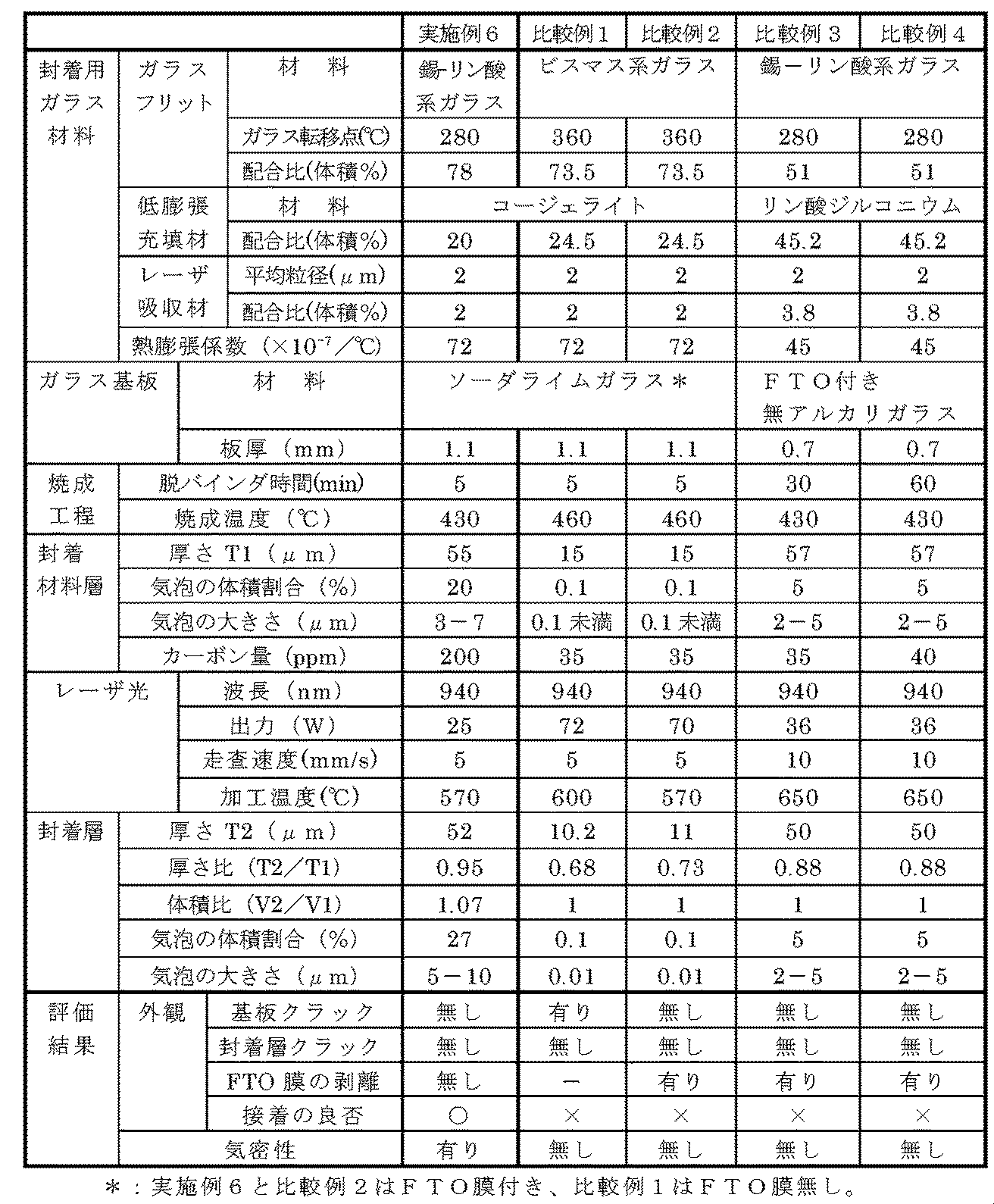
表1および表2から明らかなように、実施例1~6によるガラスパネルはいずれもガラス基板や封着層のクラック、またFTO膜の剥離が生じておらず、気密性に優れていることが分かる。これは封着材料層の溶融工程で気泡が成長し、封着材料層の膜厚減少が抑制されているためである。これに対して、FTO膜を有しないガラス基板を用いた比較例1ではガラス基板にクラックが生じ、またFTO膜を有するガラス基板を用いた比較例2~4ではFTO膜に剥離が生じ、封着層の接着状態や気密性が損なわれることが分かる。
本発明の封着材料層付きガラス部材は、対向配置された2枚のガラス基板の間に表示素子や太陽電池素子が封止されている構造を有する平板型ディスプレイ装置や太陽電池パネルを製造するために用いられるガラス基板として有用である。また本発明の電子デバイスは、上記構造を有する平板型ディスプレイ装置や太陽電池パネルである。
なお、2009年5月8日に出願された日本特許出願2009-113282号の明細書、特許請求の範囲、図面及び要約書の全内容をここに引用し、本発明の明細書の開示として、取り入れるものである。
なお、2009年5月8日に出願された日本特許出願2009-113282号の明細書、特許請求の範囲、図面及び要約書の全内容をここに引用し、本発明の明細書の開示として、取り入れるものである。
1…電子デバイス、2…第1のガラス基板、2a…素子形成領域、2b…第1の封止領域、3…第2のガラス基板、3a…第2の封止領域、4…封着層、5…封着材料層、6…電磁波、7…薄膜。
Claims (15)
- 封止領域を有するガラス基板と、
前記ガラス基板の前記封止領域上に設けられ、封着ガラスと低膨張充填材と電磁波吸収材とを含有する封着用ガラス材料の焼成層からなる封着材料層とを具備し、
前記封着材料層は、体積割合で10~30%の範囲の気泡を含むと共に、質量割合で50~200ppmの範囲の炭素を含有することを特徴とする封着材料層付きガラス部材。 - 前記気泡の大きさは0.1~50μmの範囲であることを特徴とする請求項1記載の封着材料層付きガラス部材。
- 前記低膨張充填材はシリカ、アルミナ、ジルコニア、珪酸ジルコニウム、コージェライト、リン酸ジルコニウム系化合物、ソーダライムガラスおよび硼珪酸ガラスから選ばれる少なくとも1種からなり、かつ前記封着用ガラス材料は前記低膨張充填材を体積割合で1~50%の範囲で含有することを特徴とする請求項1または請求項2記載の封着材料層付きガラス部材。
- 前記電磁波吸収材はFe、Cr、Mn、Co、NiおよびCuから選ばれる少なくとも1種の金属または前記金属を含む化合物からなり、かつ前記封着用ガラス材料は前記電磁波吸収材を体積割合で0.1~10%の範囲で含有することを特徴とする請求項1ないし請求項3のいずれか1項記載の封着材料層付きガラス部材。
- 前記封着ガラスは錫-リン酸系ガラスからなることを特徴とする請求項1ないし請求項4のいずれか1項記載の封着材料層付きガラス部材。
- 封止領域を有するガラス基板の前記封止領域上に、封着ガラスと低膨張充填材と電磁波吸収材とを含有する封着用ガラス材料層を形成し、次いで前記封着用ガラス材料層を焼成して、体積割合で10~30%の範囲の気泡を含むと共に、質量割合で50~200ppmの範囲の炭素を含有する封着材料層とすることを特徴とする封着材料層付きガラス部材の製造方法。
- 電子素子を備える素子形成領域と、前記素子形成領域の外周側に設けられた第1の封止領域とを有する第1のガラス基板と、
前記第1のガラス基板の前記第1の封止領域に対応する第2の封止領域を有し、前記第2の封止領域を有する表面が前記第1のガラス基板の前記第1の封止領域を有する表面と対向するように配置された第2のガラス基板と、
前記第1のガラス基板と前記第2のガラス基板との間を封止するように、前記第1の封止領域と前記第2の封止領域との間に形成され、封着ガラスと低膨張充填材と電磁波吸収材とを含有する封着用ガラス材料の溶融固着層からなる封着層とを具備し、
前記封着層は体積割合で10~35%の範囲の気泡を含み、かつ前記気泡の大きさが0.1~100μmの範囲であることを特徴とする電子デバイス。 - 前記第1のガラス基板および前記第2のガラス基板の少なくとも一方は、前記封止領域を有する表面に形成され、導電膜および絶縁膜から選ばれる少なくとも1種の薄膜を有することを特徴とする請求項7記載の電子デバイス。
- 電子素子を備える素子形成領域と、前記素子形成領域の外周側に設けられた第1の封止領域とを有する第1のガラス基板を用意し、
前記第1のガラス基板の前記第1の封止領域に対応する第2の封止領域と、前記第2の封止領域上に形成され、封着ガラスと低膨張充填材と電磁波吸収材とを含有する封着用ガラス材料の焼成層からなり、かつ体積割合で10~30%の範囲の気泡を含むと共に、質量割合で50~200ppmの範囲の炭素を含有する封着材料層とを有する第2のガラス基板を用意し、
前記第1のガラス基板と前記第2のガラス基板とを、前記第1の封止領域を有する表面と前記第2の封止領域を有する表面とが対向するように、前記封着材料層を介して積層し、
次いで、前記第1のガラス基板または前記第2のガラス基板を通して前記封着材料層に電磁波を照射して局所的に加熱し、前記封着材料層を溶融させて前記第1のガラス基板と前記第2のガラス基板との間を封止する封着層を形成する、
ことを特徴とする電子デバイスの製造方法。 - 前記封着材料層中に存在する前記気泡の大きさが0.1~50μmの範囲であることを特徴とする請求項9記載の電子デバイスの製造方法。
- 前記封着層は体積割合で10~35%の範囲の気泡を含み、かつ前記気泡の大きさが0.1~100μmの範囲であることを特徴とする請求項9または請求項10記載の電子デバイスの製造方法。
- 前記封着材料層の膜厚をT1、前記封着層の膜厚をT2としたとき、前記封着層は0.9T1以上1.1T1以下の範囲の膜厚T2を有することを特徴とする請求項9ないし請求項11のいずれか1項記載の電子デバイスの製造方法。
- 前記封着材料層の体積をV1、前記封着層の体積をV2としたとき、前記封着層は1V1を超えて1.15V1以下の範囲の体積V2を有することを特徴とする請求項9ないし請求項12のいずれか1項記載の電子デバイスの製造方法。
- 前記第1のガラス基板および前記第2のガラス基板の少なくとも一方は、前記封止領域を有する表面に形成され、導電膜および絶縁膜から選ばれる少なくとも1種の薄膜を有することを特徴とする請求項9ないし請求項13のいずれか1項記載の電子デバイスの製造方法。
- 前記封着材料層にレーザ光を照射して溶融させることを特徴とする請求項9ないし請求項14のいずれか1項記載の電子デバイスの製造方法。
Priority Applications (1)
| Application Number | Priority Date | Filing Date | Title |
|---|---|---|---|
| JP2011512365A JP5598469B2 (ja) | 2009-05-08 | 2010-05-07 | 封着材料層付きガラス部材とそれを用いた電子デバイスおよびその製造方法 |
Applications Claiming Priority (2)
| Application Number | Priority Date | Filing Date | Title |
|---|---|---|---|
| JP2009113282 | 2009-05-08 | ||
| JP2009-113282 | 2009-05-08 |
Publications (1)
| Publication Number | Publication Date |
|---|---|
| WO2010128679A1 true WO2010128679A1 (ja) | 2010-11-11 |
Family
ID=43050175
Family Applications (1)
| Application Number | Title | Priority Date | Filing Date |
|---|---|---|---|
| PCT/JP2010/057830 Ceased WO2010128679A1 (ja) | 2009-05-08 | 2010-05-07 | 封着材料層付きガラス部材とそれを用いた電子デバイスおよびその製造方法 |
Country Status (3)
| Country | Link |
|---|---|
| JP (1) | JP5598469B2 (ja) |
| TW (1) | TW201043586A (ja) |
| WO (1) | WO2010128679A1 (ja) |
Cited By (10)
| Publication number | Priority date | Publication date | Assignee | Title |
|---|---|---|---|---|
| WO2012090943A1 (ja) * | 2010-12-27 | 2012-07-05 | 旭硝子株式会社 | 封着材料層付きガラス部材とそれを用いた電子デバイス及びその製造方法 |
| WO2013008724A1 (ja) * | 2011-07-08 | 2013-01-17 | 旭硝子株式会社 | 複層ガラスとその製造方法 |
| WO2013140832A1 (ja) * | 2012-03-21 | 2013-09-26 | 株式会社 日立製作所 | 金属基複合材料及びその製造方法 |
| JP2013219079A (ja) * | 2012-04-04 | 2013-10-24 | Asahi Glass Co Ltd | 電子デバイスとその製造方法 |
| JP5412593B1 (ja) * | 2013-03-27 | 2014-02-12 | 株式会社フジクラ | 色素増感太陽電池素子 |
| JP2014156369A (ja) * | 2013-02-15 | 2014-08-28 | Hitachi Ltd | ガラス及びその製造方法 |
| JP2015505792A (ja) * | 2011-11-02 | 2015-02-26 | フエロ コーポレーション | 低融点ガラス系を用いた無機基材のマイクロ波シーリング |
| CN108123007A (zh) * | 2016-11-02 | 2018-06-05 | 常州亚玛顿股份有限公司 | 一种超薄双玻光伏组件的制备方法及其产物 |
| US20200123040A1 (en) * | 2017-01-26 | 2020-04-23 | Yuqi Lian | Vacuum glass and preparation method thereof |
| JP2022003682A (ja) * | 2020-05-29 | 2022-01-11 | Agc株式会社 | 封着パッケージ及び有機エレクトロルミネセンス素子 |
Families Citing this family (2)
| Publication number | Priority date | Publication date | Assignee | Title |
|---|---|---|---|---|
| JP6888561B2 (ja) * | 2018-01-31 | 2021-06-16 | 株式会社デンソー | 温度センサ |
| CN118888410A (zh) * | 2019-06-19 | 2024-11-01 | 伯恩斯公司 | 具有增强的泄漏路径长度与间隙尺寸比率的气体放电管 |
Citations (5)
| Publication number | Priority date | Publication date | Assignee | Title |
|---|---|---|---|---|
| WO1998039789A1 (fr) * | 1997-03-07 | 1998-09-11 | Hitachi, Ltd. | Panneau d'affichage a plasma |
| JP2002366050A (ja) * | 2001-06-12 | 2002-12-20 | Matsushita Electric Ind Co Ltd | 画像表示装置の製造方法、製造装置およびそれを用いて製造した画像表示装置 |
| JP2003068199A (ja) * | 2001-08-30 | 2003-03-07 | Matsushita Electric Ind Co Ltd | 表示パネルの製造方法および製造装置 |
| JP2006524419A (ja) * | 2003-04-16 | 2006-10-26 | コーニング インコーポレイテッド | フリットにより密封されたガラスパッケージおよびその製造方法 |
| JP2008115057A (ja) * | 2006-11-07 | 2008-05-22 | Electric Power Dev Co Ltd | 封止材料、ガラスパネルの製造方法および色素増感太陽電池 |
-
2010
- 2010-05-07 JP JP2011512365A patent/JP5598469B2/ja not_active Expired - Fee Related
- 2010-05-07 WO PCT/JP2010/057830 patent/WO2010128679A1/ja not_active Ceased
- 2010-05-07 TW TW099114643A patent/TW201043586A/zh unknown
Patent Citations (5)
| Publication number | Priority date | Publication date | Assignee | Title |
|---|---|---|---|---|
| WO1998039789A1 (fr) * | 1997-03-07 | 1998-09-11 | Hitachi, Ltd. | Panneau d'affichage a plasma |
| JP2002366050A (ja) * | 2001-06-12 | 2002-12-20 | Matsushita Electric Ind Co Ltd | 画像表示装置の製造方法、製造装置およびそれを用いて製造した画像表示装置 |
| JP2003068199A (ja) * | 2001-08-30 | 2003-03-07 | Matsushita Electric Ind Co Ltd | 表示パネルの製造方法および製造装置 |
| JP2006524419A (ja) * | 2003-04-16 | 2006-10-26 | コーニング インコーポレイテッド | フリットにより密封されたガラスパッケージおよびその製造方法 |
| JP2008115057A (ja) * | 2006-11-07 | 2008-05-22 | Electric Power Dev Co Ltd | 封止材料、ガラスパネルの製造方法および色素増感太陽電池 |
Cited By (19)
| Publication number | Priority date | Publication date | Assignee | Title |
|---|---|---|---|---|
| JP5494831B2 (ja) * | 2010-12-27 | 2014-05-21 | 旭硝子株式会社 | 封着材料層付きガラス部材とそれを用いた電子デバイス及びその製造方法 |
| CN103328402A (zh) * | 2010-12-27 | 2013-09-25 | 旭硝子株式会社 | 带封接材料层的玻璃构件和使用其的电子装置及其制造方法 |
| WO2012090943A1 (ja) * | 2010-12-27 | 2012-07-05 | 旭硝子株式会社 | 封着材料層付きガラス部材とそれを用いた電子デバイス及びその製造方法 |
| CN103328402B (zh) * | 2010-12-27 | 2015-07-08 | 旭硝子株式会社 | 带封接材料层的玻璃构件和使用其的电子装置及其制造方法 |
| WO2013008724A1 (ja) * | 2011-07-08 | 2013-01-17 | 旭硝子株式会社 | 複層ガラスとその製造方法 |
| JP2018108929A (ja) * | 2011-11-02 | 2018-07-12 | フエロ コーポレーション | 低融点ガラス系を用いた無機基材のマイクロ波シーリング方法、及びシーリングガラス組成物 |
| JP2015505792A (ja) * | 2011-11-02 | 2015-02-26 | フエロ コーポレーション | 低融点ガラス系を用いた無機基材のマイクロ波シーリング |
| US9490380B2 (en) | 2012-03-21 | 2016-11-08 | Hitachi, Ltd. | Metal matrix composite and method for producing the same |
| TWI485289B (zh) * | 2012-03-21 | 2015-05-21 | 日立製作所股份有限公司 | Metal matrix composite material and its manufacturing method |
| JP2013194285A (ja) * | 2012-03-21 | 2013-09-30 | Hitachi Ltd | 金属基複合材料及びその製造方法 |
| WO2013140832A1 (ja) * | 2012-03-21 | 2013-09-26 | 株式会社 日立製作所 | 金属基複合材料及びその製造方法 |
| JP2013219079A (ja) * | 2012-04-04 | 2013-10-24 | Asahi Glass Co Ltd | 電子デバイスとその製造方法 |
| JP2014156369A (ja) * | 2013-02-15 | 2014-08-28 | Hitachi Ltd | ガラス及びその製造方法 |
| JP5412593B1 (ja) * | 2013-03-27 | 2014-02-12 | 株式会社フジクラ | 色素増感太陽電池素子 |
| CN108123007A (zh) * | 2016-11-02 | 2018-06-05 | 常州亚玛顿股份有限公司 | 一种超薄双玻光伏组件的制备方法及其产物 |
| CN108123007B (zh) * | 2016-11-02 | 2019-11-26 | 常州亚玛顿股份有限公司 | 一种超薄双玻光伏组件的制备方法及其产物 |
| US20200123040A1 (en) * | 2017-01-26 | 2020-04-23 | Yuqi Lian | Vacuum glass and preparation method thereof |
| JP2022003682A (ja) * | 2020-05-29 | 2022-01-11 | Agc株式会社 | 封着パッケージ及び有機エレクトロルミネセンス素子 |
| JP7807197B2 (ja) | 2020-05-29 | 2026-01-27 | Agc株式会社 | 封着パッケージ及び有機エレクトロルミネセンス素子 |
Also Published As
| Publication number | Publication date |
|---|---|
| JPWO2010128679A1 (ja) | 2012-11-01 |
| JP5598469B2 (ja) | 2014-10-01 |
| TW201043586A (en) | 2010-12-16 |
Similar Documents
| Publication | Publication Date | Title |
|---|---|---|
| JP5598469B2 (ja) | 封着材料層付きガラス部材とそれを用いた電子デバイスおよびその製造方法 | |
| JP5673102B2 (ja) | 封着材料層付きガラス部材およびそれを用いた電子デバイスとその製造方法 | |
| JP5500079B2 (ja) | 封着材料層付きガラス部材とその製造方法、および電子デバイスとその製造方法 | |
| JP5413373B2 (ja) | レーザ封着用ガラス材料、封着材料層付きガラス部材、および電子デバイスとその製造方法 | |
| JP5418594B2 (ja) | 封着材料層付きガラス部材とそれを用いた電子デバイスおよびその製造方法 | |
| JP5716743B2 (ja) | 封着材料ペーストとそれを用いた電子デバイスの製造方法 | |
| WO2010055888A1 (ja) | 封着材料層付きガラス部材の製造方法と電子デバイスの製造方法 | |
| JP2010228998A (ja) | 封着材料層付きガラス部材とそれを用いた電子デバイスおよびその製造方法 | |
| US20150037594A1 (en) | Glass composition, sealing material, and sealed package | |
| JPWO2014092013A1 (ja) | 封着材料、封着材料層付き基板、積層体および電子デバイス | |
| TW201246527A (en) | Glass member with sealing material layer, electronic device using same and method for producing same | |
| US20130284266A1 (en) | Electronic device and manufacturing method thereof | |
| WO2010137667A1 (ja) | 封着材料層付きガラス部材とそれを用いた電子デバイスおよびその製造方法 | |
| JP5370011B2 (ja) | 封着材料層付きガラス部材の製造方法と電子デバイスの製造方法 | |
| JP2013119501A (ja) | 封着材料層付きガラス部材および気密部材の製造方法 | |
| JP5516194B2 (ja) | 光加熱封着用ガラス、封着材料層付きガラス部材、及び電子デバイスとその製造方法 | |
| JP2014240344A (ja) | 封着材料層付き部材、電子デバイス、および電子デバイスの製造方法 | |
| JP2013053032A (ja) | 気密部材とその製造方法 |
Legal Events
| Date | Code | Title | Description |
|---|---|---|---|
| 121 | Ep: the epo has been informed by wipo that ep was designated in this application |
Ref document number: 10772196 Country of ref document: EP Kind code of ref document: A1 |
|
| WWE | Wipo information: entry into national phase |
Ref document number: 2011512365 Country of ref document: JP |
|
| NENP | Non-entry into the national phase |
Ref country code: DE |
|
| 122 | Ep: pct application non-entry in european phase |
Ref document number: 10772196 Country of ref document: EP Kind code of ref document: A1 |