WO2010119811A1 - マスクブランク及び転写用マスク並びに膜緻密性評価方法 - Google Patents
マスクブランク及び転写用マスク並びに膜緻密性評価方法 Download PDFInfo
- Publication number
- WO2010119811A1 WO2010119811A1 PCT/JP2010/056409 JP2010056409W WO2010119811A1 WO 2010119811 A1 WO2010119811 A1 WO 2010119811A1 JP 2010056409 W JP2010056409 W JP 2010056409W WO 2010119811 A1 WO2010119811 A1 WO 2010119811A1
- Authority
- WO
- WIPO (PCT)
- Prior art keywords
- film
- thin film
- density
- mask blank
- mask
- Prior art date
- Legal status (The legal status is an assumption and is not a legal conclusion. Google has not performed a legal analysis and makes no representation as to the accuracy of the status listed.)
- Ceased
Links
Images


Classifications
-
- G—PHYSICS
- G03—PHOTOGRAPHY; CINEMATOGRAPHY; ANALOGOUS TECHNIQUES USING WAVES OTHER THAN OPTICAL WAVES; ELECTROGRAPHY; HOLOGRAPHY
- G03F—PHOTOMECHANICAL PRODUCTION OF TEXTURED OR PATTERNED SURFACES, e.g. FOR PRINTING, FOR PROCESSING OF SEMICONDUCTOR DEVICES; MATERIALS THEREFOR; ORIGINALS THEREFOR; APPARATUS SPECIALLY ADAPTED THEREFOR
- G03F1/00—Originals for photomechanical production of textured or patterned surfaces, e.g., masks, photo-masks, reticles; Mask blanks or pellicles therefor; Containers specially adapted therefor; Preparation thereof
- G03F1/50—Mask blanks not covered by G03F1/20 - G03F1/34; Preparation thereof
-
- G—PHYSICS
- G03—PHOTOGRAPHY; CINEMATOGRAPHY; ANALOGOUS TECHNIQUES USING WAVES OTHER THAN OPTICAL WAVES; ELECTROGRAPHY; HOLOGRAPHY
- G03F—PHOTOMECHANICAL PRODUCTION OF TEXTURED OR PATTERNED SURFACES, e.g. FOR PRINTING, FOR PROCESSING OF SEMICONDUCTOR DEVICES; MATERIALS THEREFOR; ORIGINALS THEREFOR; APPARATUS SPECIALLY ADAPTED THEREFOR
- G03F1/00—Originals for photomechanical production of textured or patterned surfaces, e.g., masks, photo-masks, reticles; Mask blanks or pellicles therefor; Containers specially adapted therefor; Preparation thereof
- G03F1/54—Absorbers, e.g. of opaque materials
-
- G—PHYSICS
- G03—PHOTOGRAPHY; CINEMATOGRAPHY; ANALOGOUS TECHNIQUES USING WAVES OTHER THAN OPTICAL WAVES; ELECTROGRAPHY; HOLOGRAPHY
- G03F—PHOTOMECHANICAL PRODUCTION OF TEXTURED OR PATTERNED SURFACES, e.g. FOR PRINTING, FOR PROCESSING OF SEMICONDUCTOR DEVICES; MATERIALS THEREFOR; ORIGINALS THEREFOR; APPARATUS SPECIALLY ADAPTED THEREFOR
- G03F1/00—Originals for photomechanical production of textured or patterned surfaces, e.g., masks, photo-masks, reticles; Mask blanks or pellicles therefor; Containers specially adapted therefor; Preparation thereof
- G03F1/26—Phase shift masks [PSM]; PSM blanks; Preparation thereof
- G03F1/32—Attenuating PSM [att-PSM], e.g. halftone PSM or PSM having semi-transparent phase shift portion; Preparation thereof
-
- G—PHYSICS
- G03—PHOTOGRAPHY; CINEMATOGRAPHY; ANALOGOUS TECHNIQUES USING WAVES OTHER THAN OPTICAL WAVES; ELECTROGRAPHY; HOLOGRAPHY
- G03F—PHOTOMECHANICAL PRODUCTION OF TEXTURED OR PATTERNED SURFACES, e.g. FOR PRINTING, FOR PROCESSING OF SEMICONDUCTOR DEVICES; MATERIALS THEREFOR; ORIGINALS THEREFOR; APPARATUS SPECIALLY ADAPTED THEREFOR
- G03F1/00—Originals for photomechanical production of textured or patterned surfaces, e.g., masks, photo-masks, reticles; Mask blanks or pellicles therefor; Containers specially adapted therefor; Preparation thereof
- G03F1/38—Masks having auxiliary features, e.g. special coatings or marks for alignment or testing; Preparation thereof
- G03F1/46—Antireflective coatings
-
- G—PHYSICS
- G03—PHOTOGRAPHY; CINEMATOGRAPHY; ANALOGOUS TECHNIQUES USING WAVES OTHER THAN OPTICAL WAVES; ELECTROGRAPHY; HOLOGRAPHY
- G03F—PHOTOMECHANICAL PRODUCTION OF TEXTURED OR PATTERNED SURFACES, e.g. FOR PRINTING, FOR PROCESSING OF SEMICONDUCTOR DEVICES; MATERIALS THEREFOR; ORIGINALS THEREFOR; APPARATUS SPECIALLY ADAPTED THEREFOR
- G03F1/00—Originals for photomechanical production of textured or patterned surfaces, e.g., masks, photo-masks, reticles; Mask blanks or pellicles therefor; Containers specially adapted therefor; Preparation thereof
- G03F1/68—Preparation processes not covered by groups G03F1/20 - G03F1/50
- G03F1/82—Auxiliary processes, e.g. cleaning or inspecting
- G03F1/84—Inspecting
-
- Y—GENERAL TAGGING OF NEW TECHNOLOGICAL DEVELOPMENTS; GENERAL TAGGING OF CROSS-SECTIONAL TECHNOLOGIES SPANNING OVER SEVERAL SECTIONS OF THE IPC; TECHNICAL SUBJECTS COVERED BY FORMER USPC CROSS-REFERENCE ART COLLECTIONS [XRACs] AND DIGESTS
- Y10—TECHNICAL SUBJECTS COVERED BY FORMER USPC
- Y10T—TECHNICAL SUBJECTS COVERED BY FORMER US CLASSIFICATION
- Y10T428/00—Stock material or miscellaneous articles
- Y10T428/24—Structurally defined web or sheet [e.g., overall dimension, etc.]
- Y10T428/24802—Discontinuous or differential coating, impregnation or bond [e.g., artwork, printing, retouched photograph, etc.]
-
- Y—GENERAL TAGGING OF NEW TECHNOLOGICAL DEVELOPMENTS; GENERAL TAGGING OF CROSS-SECTIONAL TECHNOLOGIES SPANNING OVER SEVERAL SECTIONS OF THE IPC; TECHNICAL SUBJECTS COVERED BY FORMER USPC CROSS-REFERENCE ART COLLECTIONS [XRACs] AND DIGESTS
- Y10—TECHNICAL SUBJECTS COVERED BY FORMER USPC
- Y10T—TECHNICAL SUBJECTS COVERED BY FORMER US CLASSIFICATION
- Y10T428/00—Stock material or miscellaneous articles
- Y10T428/31504—Composite [nonstructural laminate]
Definitions
- the present invention relates to a transfer mask used as a mask during fine pattern transfer in the process of manufacturing a semiconductor element, a mask blank as an intermediate that can be formed into a transfer mask by performing a certain processing, and a mask blank formed thereon.
- the present invention relates to a film density evaluation method for evaluating the density of a thin film.
- a fine pattern is formed using a photolithography method. Further, a number of substrates called transfer masks are usually used for forming this fine pattern.
- This transfer mask is generally provided with a fine pattern made of a metal thin film or the like on a light-transmitting glass substrate, and a photolithography method is also used in the manufacture of this transfer mask.
- a mask blank having a thin film (for example, a light shielding film) for forming a transfer pattern (mask pattern) on a light-transmitting substrate such as a glass substrate is used.
- the production of a transfer mask using this mask blank is performed by forming a desired fine pattern on a resist film coated on the mask blank and etching the thin film according to the resist pattern. For this reason, the characteristics of the thin film formed on the mask blank as an intermediate substantially affect the performance of the transfer mask.
- Patent Document 1 points out that it is necessary to reduce the thickness of the resist film in order to cope with the miniaturization of the transfer pattern. Since the chromium-based material that has been used as a transfer pattern thin film in the past is dry-etched with a chlorine-based gas containing oxygen, the resist pattern is also susceptible to damage during etching. Is said to be difficult.
- tantalum or molybdenum silicide that can be dry-etched with a fluorine-based gas is applied as a transfer pattern thin film material that can be used for resist thinning, and chromium having a high etching selectivity with respect to a fluorine-based gas, etc.
- a laminated structure provided with a so-called hard mask film is proposed. By using this laminated structure, the pattern transfer to the transfer pattern thin film can be performed by dry etching using the hard mask film as a mask. Therefore, the resist film has a thickness sufficient to transfer the pattern to the hard mask film. It will be better if there is.
- the resist can be made thinner than the case where the resist film is directly transferred to a thin film containing chromium as a main component, A reasonable effect was obtained.
- the phase shift film which is a film for forming a transfer pattern at the time of mask preparation, includes a metal silicide like the MoSiOC film described in Patent Document 2. Materials have been widely used.
- in-plane dimensional uniformity of the transfer pattern is important in order to obtain a desired transfer result on the wafer. According to the roadmap ITRS 2008 updade published by the International Semiconductor Roadmap Committee, the mask pattern dimension uniformity within the mask plane is required to be 2.0 nm or less in lithography with DRAM half pitch less than 45 nm. .
- the present inventors have changed the line width by irradiating an ArF excimer laser as an exposure light source over a period of repeated use of the previous mask. Clarified that the phenomenon of fattening occurs.
- the present inventors investigated the pattern of a metal silicide thin film (thin film containing metal and silicon as main components) in a transfer mask in which a change in line width (thickening) occurred due to repeated use. As a result, as shown in FIG. 5, an altered layer 2 ′ containing Si, O, and some metal (eg, Mo) is formed on the surface layer side of the metal silicide-based thin film 2 (eg, MoSi-based film).
- the reason (mechanism) for generating such an altered layer is considered as follows. That is, the conventional metal silicide-based thin film (for example, MoSi-based film) formed by sputtering has a structural gap, and even if annealing is performed after film formation, the change in the structure of the metal silicide-based thin film (for example, MoSi film) is small. Therefore, in the process of using the photomask, for example, oxygen (O 2 ) or water (H 2 O) in the atmosphere enters the gap, and further, oxygen (O 2 ) in the atmosphere reacts with the ArF excimer laser. Generated ozone (O 3 ) or the like enters the gap and reacts with Si or Mo constituting a metal silicide-based thin film (for example, MoSi-based film).
- oxygen (O 2 ) or water (H 2 O) in the atmosphere enters the gap, and further, oxygen (O 2 ) in the atmosphere reacts with the ArF excimer laser.
- Si and metal M (for example, Mo) constituting a metal silicide-based thin film (for example, MoSi-based film) in such an environment are excited and exposed to a transition state when irradiated with exposure light (especially, short wavelength light such as ArF). Then, Si oxidizes and expands (because the volume of SiO 2 is larger than Si), and metal M (for example, Mo) also oxidizes to generate an altered layer on the surface layer side of the metal silicide-based thin film (for example, MoSi-based film). Is done. At this time, the quality of the generated Si oxide film varies greatly depending on the amount of moisture (humidity) in the atmosphere, and the lower the density, the lower the density of the Si oxide film.
- exposure light especially, short wavelength light such as ArF
- the transfer mask When the transfer mask is repeatedly used in an environment where a low-density Si oxide film is formed, when exposure light is accumulated, the oxidation and expansion of Si further progress, and oxidation occurs at the interface between the bulk and the deteriorated layer.
- the diffused metal M for example, Mo
- the diffused metal M diffuses in the modified layer, precipitates on the surface, and sublimates as, for example, an oxide of the metal M (for example, MoO 3 ), and the density of the modified layer is further reduced and oxidized. It becomes easy. As a result, it is considered that the thickness of the altered layer gradually increases (the proportion of the altered layer in the metal silicide-based thin film (eg, MoSi film) increases).
- both a thin film of metal silicide and a thin film mainly composed of tantalum, ozone (O 3 ) or the like is formed in a slight structural gap of the film. Oxidation progresses due to the penetration of metal, and the formation of altered layers is remarkable in metal silicide thin films with relatively large gaps in the structure. Focusing on the fact that there is little formation, if the pattern is formed with a dense light-shielding film with few vacancies so that ozone (O 3 ) or the like does not progress inside the thin film, the transfer pattern can be changed during exposure using an ArF excimer laser. It was found that the in-plane dimensional change can be reduced.
- the film density as an index of the thin film density.
- the density of the thin film can be determined by an XRR (X-Ray Reflectivity) method or the like.
- the lower limit of the film density at which sufficient light resistance to ArF exposure light can be obtained varies depending on the film composition even if the same metal silicide material is used. Therefore, the lower limit of the film density must be determined for each film composition. In other words, the index was found to be very low in versatility.
- the present inventors have ascertained the lower limit of the film density with various compositions using various metal silicide materials, and as a result, the film density is such that light resistance to ArF exposure light in a thin film having a certain film composition can be obtained.
- the lower limit value of the relative density tends to be a predetermined value or more even for thin films having different film compositions. I found.
- the lower limit value of the relative density is different from that of the metal silicide-based material, even in a thin film mainly composed of tantalum, if the lower limit value of the film density at which light resistance to ArF exposure light is obtained is converted into the relative density, It has been found that even for tantalum-based thin films having different film compositions, the lower limit of their relative values tends to be a predetermined value or more.
- the present invention has the following configuration.
- (Configuration 1) A mask blank used for producing a transfer mask to which ArF exposure light is applied, and having a thin film for forming a transfer pattern on a transparent substrate,
- the thin film is made of a material mainly composed of tantalum (Ta),
- the actual density of the thin film is d1
- d (relative density) (d1 / d2) ⁇ 100
- a relative density d of the thin film represented by the formula is greater than 83%.
- the thin film includes tantalum (Ta) as a main component, 2.
- (Configuration 3) A mask blank used for producing a transfer mask to which ArF exposure light is applied, and having a thin film for forming a transfer pattern on a transparent substrate,
- the thin film is made of a material mainly composed of silicon (Si) and a transition metal,
- the actual density of the thin film is d1
- d (relative density) (d1 / d2) ⁇ 100
- a relative density d of the thin film represented by the formula is greater than 94%.
- the thin film includes silicon (Si), Titanium (Ti), vanadium (V), niobium (Nb), molybdenum (Mo), zirconium (Zr), ruthenium (Ru), rhodium (Rh), chromium (Cr), nickel (Ni), hafnium (Hf), 4.
- the thin film is a light shielding film that shields exposure light,
- a mask blank including a thin film for forming a transfer pattern made of a material containing Ta as a main component is calculated from the film composition of the thin film as the actual density d1 of the thin film.
- a change in pattern dimension caused by oxidation of the surface of the thin film by irradiation with ArF exposure light is small, and a mask blank having a long lifetime can be obtained, and high reliability as a mask blank can be obtained.
- an evaluation index called relative density the denseness can be quantitatively evaluated even for thin films having different compositions, and the relationship between the relative density and the mask blank lifetime is clarified. It becomes possible. A long-life and highly reliable mask blank can be obtained.
- the thin film is made of tantalum (Ta) as a main component and one or more elements selected from boron (B), carbon (C), nitrogen (N), and oxygen (O).
- Ta tantalum
- B boron
- C carbon
- N nitrogen
- O oxygen
- the relationship between the relative density d and the mask blank lifetime is preferably used in the mask blank constituted by
- a mask blank including a thin film for forming a transfer pattern made of a material mainly composed of silicon (Si) and a transition metal, where the actual density of the thin film is d1, and the thin film
- the thin film is made of silicon (Si), titanium (Ti), vanadium (V), niobium (Nb), molybdenum (Mo), zirconium (Zr), ruthenium (Ru), rhodium ( Rh), chromium (Cr), nickel (Ni), hafnium (Hf), tantalum (Ta), and a mask blank composed of one or more transition metals selected from tungsten (W), in particular, relative density d And the mask blank lifetime are preferably used.
- the actual density d1 of the thin film is such that the film thickness as the thin film of the mask blank is very thin by applying the XRR density calculated by the XRR method. This is preferable because the film density can be calculated.
- the denseness of the thin film can be quantitatively evaluated based on the relative density d, and the relationship between the relative density and the mask blank lifetime can be clarified. Further, by using this evaluation method, it becomes an index for reliability evaluation, and it is possible to improve productivity.
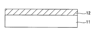
- FIG. 1 is a sectional view showing an embodiment of a mask blank according to the present invention.
- the mask blank according to the present embodiment has a thin film 12 for forming a transfer pattern on a transparent substrate 11, and is used for producing a transfer mask.
- the mask blank, on the transparent substrate 11, for example, can be obtained by forming Ta x B y, Ta x N y, a thin film 12 made of Mo x Si y or Ta x Si y by sputtering or the like.
- the thin film 12 functions as a light-shielding film of a transfer mask by being patterned by a photolithography method.
- Example 1 For Ta x B y film
- a thin film for the case of Ta x B y described Examples and Comparative Examples.
- DC sputtering reactive sputtering
- Example 1-2 Similar to Example 1-1, a Ta x B y film is formed on the transparent substrate.
- the difference from Example 1-1 is that the gas pressure in the film forming apparatus was changed.
- the gas pressure is 0.303 Pa, and the power of the DC power source as 1.5 kW, by reactive sputtering (DC sputtering), thereby forming a Ta x B y film of tantalum and boron with a film thickness of 50nm.
- DC sputtering reactive sputtering
- Example 1-3 Similar to Example 1-1, a Ta x B y film is formed on the transparent substrate.
- the difference from Example 1-1 is that the gas pressure in the film forming apparatus was changed.
- the gas pressure is 0.562 Pa, and the power of the DC power source as 1.5 kW, by reactive sputtering (DC sputtering), thereby forming a Ta x B y film of tantalum and boron with a film thickness of 50nm.
- Example 1 Similar to Example 1-1, a Ta x B y film is formed on the transparent substrate.
- the difference from Example 1-1 is that the gas pressure in the film forming apparatus was changed.
- the gas pressure is 0.911 Pa, and the power of the DC power source as 1.5 kW, by reactive sputtering (DC sputtering), thereby forming a Ta x B y film of tantalum and silicon in a film thickness of 50nm.
- Example 1-4 Similar to Example 1-1, a Ta x B y film is formed on the transparent substrate.
- Ta tantalum
- B boron
- Example 1-5 Similar to Example 1-4 above, a Ta x B y film is formed on the transparent substrate.
- the sputtering gas in the film forming apparatus was produced by changing the type and gas pressure.
- the gas pressure is 0.193 Pa, and the power of the DC power source as 1.5 kW, by reactive sputtering (DC sputtering), thereby forming a Ta x B y film of tantalum and boron with a film thickness of 50nm.
- DC sputtering reactive sputtering
- Table 1 The literature values used for the calculation are listed in Table 1.
- the analysis method for determining the actual composition of Ta x B y film XPS (X-ray photoelectron spectroscopy), AES (atomic emission spectroscopy) using RBS (Rutherford backscattering spectrometry).
- Example 2 Ta x N y film
- DC sputtering reactive sputtering
- Example 2-2 Similar to Example 2-1, a Ta x N y film is formed on the transparent substrate.
- the difference from Example 2-1 is that the flow rate ratio of xenon gas and nitrogen gas was changed.
- the gas pressure is 0.076 Pa, and the power of the DC power supply is 1.5 kW
- a Ta x N y film having a thickness of 50 nm was formed by reactive sputtering (DC sputtering).
- Example 2-3 Similar to Example 2-1, a Ta x N y film is formed on the transparent substrate.
- the difference from Example 2-1 is that the flow rate ratio of xenon gas and nitrogen gas was changed.
- the gas pressure is 0.075 Pa
- the power of the DC power source is 1.5 kW
- a Ta x N y film having a thickness of 50 nm was formed by reactive sputtering (DC sputtering).
- Example 2-1 Ta x N y film Similar to Example 2-1, a Ta x N y film is formed on the transparent substrate. The difference from Example 2-1 is that the flow rate ratio of xenon gas and nitrogen gas was changed.
- gas pressure 0.075 Pa
- DC power supply is 1.5 kW
- a Ta x N y film having a thickness of 50 nm was formed by reactive sputtering (DC sputtering).
- the sputtering gas is only a rare gas (xenon gas) and a Ta film is formed on a transparent substrate.
- a Ta target a Ta film was formed to a thickness of 50 nm by reactive sputtering (DC sputtering) in a xenon (Xe) gas atmosphere with a gas pressure of 0.075 Pa and a DC power source power of 1.5 kW.
- Example 2 In the same manner as in Example 1, the relative densities d of Examples 2-1 to 2-3, Comparative Example 2-1, and Comparative Example 2-2 were determined.
- the XRR calculated density (actual density) d1 of the Ta x N y film was determined using the XRR (X-ray reflectivity) method.
- the theoretical density d2 was calculated from literature values.
- the literature values used for the calculation are listed in Table 3.
- Example 3 Mo x Si y film
- Ar argon
- the power of the DC power source was 2.0 kW
- a Mo x Si y film made of molybdenum and silicon was formed to a thickness of 50 nm by reactive sputtering (DC sputtering).
- Example 3 Comparative Example 3: Mo x Si y film
- a Mo x Si y film is formed on the transparent substrate.
- the difference from Example 3-1 is that the gas pressure in the film forming apparatus was changed. In an argon (Ar) gas atmosphere, a gas pressure of 0.484 Pa, a DC power supply power of 2.0 kW, and a reactive sputtering (DC sputtering) to form a Mo x Si y film made of molybdenum and silicon with a thickness of 50 nm. did.
- Ar argon
- DC sputtering reactive sputtering
- Example 3-3 Similar to Example 3-1, a Mo x Si y film is formed on the transparent substrate.
- the difference from Example 3-1 is that the sputtering target used was changed.
- the gas pressure is 0.206 Pa
- the power of the DC power source was set to 2.0 kW
- a Mo x Si y film made of molybdenum and silicon was formed to a thickness of 50 nm by reactive sputtering (DC sputtering).
- DC sputtering reactive sputtering
- DC sputtering reactive sputtering
- the relative densities d of Examples 3-1 to 3-4 and Comparative Example 3 were determined.
- the XRR calculated density (actual density) d1 of the Mo x Si y film was determined using the XRR method.
- the theoretical density d2 was determined from literature values.
- the literature values used for the calculation are listed in Table 5.
- Example 4 Ta x Si y film
- DC sputtering reactive sputtering
- Example 4 Similar to Example 4-1, a Ta x Si y film is formed on the transparent substrate.
- the difference from Example 4-1 is that the gas pressure in the film forming apparatus was changed.
- the gas pressure is 0.484 Pa, and the power of the DC power source was set to 1.5 kW, and a TaSi film made of tantalum and silicon was formed to a thickness of 50 nm by reactive sputtering (DC sputtering).
- Example 4-1 and Comparative Example 4 was determined.
- the XRR calculation density (actual density) d1 of the Ta x Si y film was determined using the XRR method.
- the literature values used for the calculation are shown in Table 7.
- the pattern dimension change by ArF excimer laser irradiation was performed by irradiating the thin film with ArF excimer laser, observing the cross section with a TEM (transmission electron microscope), and regarding the thickness of the altered layer on the surface as the pattern dimension change.
- the grounds are described below. Since the surface alteration is mainly caused by oxidation, it is accompanied by an increase in the film thickness and a decrease in the light shielding property of the altered layer portion.
- An increase in the thickness of the thin film corresponds to a change in pattern dimension on the pattern side wall, and a decrease in light shielding performance is regarded as a substantial change in pattern dimension in exposure.
- the thickness of the deteriorated layer is equivalent to a change in pattern dimension that affects exposure.
- the thickness of the altered layer is 2.0 nm or less satisfies the requirement that the dimensional uniformity of the mask is 2.4 nm or less in photolithography with a half pitch of less than 45 nm.
- Table 9 shows the relative density and the thickness of the altered layer in each example and comparative example.
- Example 1-1 The thickness of the deteriorated layer was 2.0 nm even when the relative density d was 88.5% (Example 1-5), the lowest among the results of Example 1-5.
- the thickness of the deteriorated layer is set to 2 by increasing the relative density to more than 83% (more preferably 84% or more). 0.0 nm or less. That is, it can be seen that such a thin film has durability against exposure light irradiation to which an ArF excimer laser that is currently widely used is applied. Thereby, a long lifetime can be obtained and high reliability can be obtained.
- the thickness of the altered layer can be made 2.0 nm or less by making the relative density greater than 94% (more preferably 95% or more). That is, it can be seen that such a thin film is also durable against exposure light to which an ArF excimer laser is applied.
- the thin film includes tantalum (Ta) and boron (B) as main components. It may be composed of a binary material composed of one element selected from carbon (C), nitrogen (N), and oxygen (O), and similarly has a relative density greater than 83% (more preferably 84% or more), a high film density can be obtained, so that it has light resistance to exposure light and can reduce a change in mask dimensions.
- the theoretical density may be calculated by the same method as in Example 1 on the basis of each literature value assuming a mixture of Ta and Ta 2 O 5 .
- the theoretical density may be calculated by the same method as in Example 1 on the basis of each literature value assuming a mixture of TaC and Ta or C.
- the thin film has a ternary system or more composed of tantalum (Ta) as a main component and two or more elements selected from boron (B), carbon (C), nitrogen (N), and oxygen (O). You may be comprised with material and the same effect can be acquired.
- Ta tantalum
- B boron
- C carbon
- N nitrogen
- O oxygen
- d2 As a calculation method of the theoretical density d2 at this time, for example, in the case where the thin film is a Ta x O y N z film, it is assumed that it is a mixture of two or more selected from Ta, TaN, and Ta 2 O 5. Thus, it may be calculated by the same method as in the first embodiment based on each document value. For example, when the thin film is a Ta x B y N z film, it is assumed that the thin film is a mixture of two or more selected from Ta, B, TaB 2 , and TaN. The theoretical density may
- the thin film is a Ta x C y N z film
- the thin film is a mixture of two or more selected from Ta, C, TaC, and TaN, and the same as in Example 1 based on each literature value.
- the theoretical density should be calculated using For example, in the case where the thin film is a Ta x B y O z film, it is assumed that the thin film is a mixture of two or more selected from Ta, B, TaB 2 , and Ta 2 O 5.
- the theoretical density may be calculated by the same method as in Example 1.
- the thin film is a Ta x C y O z film
- the thin film is a mixture of two or more selected from Ta, C, TaC, and Ta 2 O 5 , and the examples are based on each literature value.
- the theoretical density may be calculated by the same method as in 1.
- the thin film is a Ta w C x O y N z film
- each literature value is assumed assuming that the thin film is a mixture of three or more selected from Ta, C, TaC, Ta 2 O 5 , and TaN.
- the theoretical density may be calculated by the same method as in the first embodiment.
- the thin film is a Ta w B x O y N z film
- the theoretical density may be calculated by the same method as in the first embodiment.
- MoSi and TaSi have been described as thin films made of a material containing a transition metal, silicon (Si), titanium (Ti), vanadium (V), niobium (Nb), zirconium (Zr), ruthenium are also described.
- Ru rhodium (Rh), chromium (Cr), nickel (Ni), hafnium (Hf) and tungsten (W), and may be composed of a binary material of one transition metal.
- the relative density is higher than 94% (more preferably 95% or more)
- high film density can be obtained, so that it has light resistance to exposure light and can reduce a change in mask dimensions.
- the theoretical density d2 at this time for example, when the thin film is a Zr x Si y film, it is assumed that it is a mixture of two or more selected from Zr, Si, and ZrSi 2 . It is good to calculate with the same method based on the value. For example, in the case where the thin film is a W x Si y film, the theoretical density is calculated by the same method based on each literature value, assuming that it is a mixture of two or more selected from W, Si, and WSi 2 Good.
- the thin film is a Ti x Si y film
- the thin film is a mixture of two or more selected from Ti, Si, and TiSi 2 , and the same method as in Example 1 is used based on the values of each document. It is good to calculate the theoretical density.
- the theoretical density is calculated by the same method based on each literature value, assuming that it is a mixture of two or more selected from Cr, Si, and CrSi 2 Good.
- the theoretical density is calculated by the same method based on each literature value on the assumption that it is a mixture of two or more selected from Nb, Si, and NbSi 2 Good.
- the thin film is an Hf x Si y film
- the thin film is a mixture of two or more selected from Hf, Si, and HfSi 2 , and the same method as in Example 1 is used based on each literature value. It is good to calculate the theoretical density.
- the theoretical density is calculated by the same method based on each literature value, assuming that the thin film is a mixture of two or more selected from V, Si, and VSi 2 Good.
- the theoretical density is calculated by the same method based on each literature value, assuming that the thin film is a mixture of two or more selected from Ru, Si, and RuSi 2 Good.
- the thin film is a Ni x Si y film
- the thin film is a mixture of two or more selected from Ni, Si, and NiSi 2 , and the same method as in Example 1 is used based on the values of each document. It is good to calculate the theoretical density.
- the thin film is made of silicon (Si), titanium (Ti), vanadium (V), niobium (Nb), zirconium (Zr), ruthenium (Ru), rhodium (Rh), chromium (Cr), nickel (Ni).
- a thin film made of a material containing a transition metal silicon (Si), titanium (Ti), vanadium (V), niobium (Nb), zirconium (Zr), ruthenium (Ru), rhodium (Rh), chromium ( In addition to one or more transition metals selected from Cr), nickel (Ni), hafnium (Hf) and tungsten (W), one or more selected from carbon (C), nitrogen (N) and oxygen (O) It may be composed of a ternary or higher material composed of an element, and the same effect can be obtained.
- the thin film is a Mo x Si y O z film
- the mixture is selected from Mo, Si, MoSi 2 , MoO 3 , and SiO 2.
- the thin film is a mixture selected from Mo, Si, MoSi 2 , MoN, and Si 3 N 4 , and the same values are obtained based on each literature value. It is good to calculate the theoretical density by the method.
- the thin film is a Mo w Si x O y N z film
- the thin film is a mixture selected from Mo, Si, MoSi 2 , MoN, Si 3 N 4 , MoO 3 , and SiO 2 .
- the theoretical density may be calculated by the same method based on each literature value.
- the thin film is a Mo x Si y C z film
- the thin film is a mixture selected from Mo, Si, C, MoSi 2 , Mo 2 C, and SiC, and the same applies based on each literature value.
- the theoretical density should be calculated using For example, when the thin film is a Mo w Si x C y N z film, it is assumed that the thin film is a mixture selected from Mo, Si, C, MoSi 2 , MoN, Si 3 N 4 , Mo 2 C, and SiC.
- the theoretical density may be calculated by the same method based on each literature value.
- the thin film is a Mo v Si w O x C y N z film is selected Mo, Si, C, MoSi 2 , MoO 3, SiO 2, MoN, Si 3 N 4, Mo 2 C, and SiC
- the theoretical density may be calculated by a similar method based on the literature values.
- the thin film is a Zr x Si y O z film
- the thin film is a mixture selected from Zr, Si, ZrSi 2 , ZrO 2 , and SiO 2
- the theoretical density should be calculated using For example, in the case where the thin film is a Zr x Si y N z film, it is assumed that the thin film is a mixture selected from Zr, Si, ZrSi 2 , ZrN, and Si 3 N 4 , and the same values are obtained based on each literature value. It is good to calculate the theoretical density by the method.
- the thin film is a Zr w Si x O y N z film
- the thin film is a mixture selected from Zr, Si, ZrSi 2 , ZrN, Si 3 N 4 , ZrO 2 , and SiO 2 .
- the theoretical density may be calculated by the same method based on each literature value.
- the thin film is a Zr x Si y C z film
- the thin film is a mixture selected from Zr, Si, C, ZrSi 2 , ZrC, and SiC
- a similar method is performed based on the values of each document.
- Calculate the theoretical density with For example, in the case where the thin film is a Zr w Si x C y N z film, assuming that the thin film is a mixture selected from Zr, Si, C, ZrSi 2 , ZrN, Si 3 N 4 , ZrC, and SiC, The theoretical density may be calculated by the same method based on each literature value.
- mixed thin film in the case of Zr v Si w O x C y N z film Zr, Si, C, ZrSi 2, ZrO 2, SiO 2, ZrN, selected from Si 3 N 4, ZrC, and SiC It is better to calculate the theoretical density by the same method based on the values of each document, assuming that it is a body.
- the thin film is a W x Si y O z film
- the thin film is a mixture selected from W, Si, WSi 2 , WO 3 , and SiO 2 , and the same applies based on each literature value.
- the theoretical density should be calculated using For example, in the case where the thin film is a W x Si y N z film, it is assumed that the thin film is a mixture selected from W, Si, WSi 2 , WN, and Si 3 N 4 , and the same values are obtained based on each literature value. It is good to calculate the theoretical density by the method.
- the thin film is a W w Si x O y N z film
- W, Si assuming that the WSi 2, WN, Si 3 N 4, WO 3, and mixtures thereof selected from SiO 2
- the theoretical density may be calculated by the same method based on each literature value.
- the thin film is a W x Si y C z film
- the thin film is a mixture selected from W, Si, C, WSi 2 , W 2 C, and SiC, and the same applies based on each literature value.
- the theoretical density should be calculated using For example, in the case the thin film is a W w Si x C y N z film assumes W, Si, C, WSi 2 , WN, Si 3 N 4, W 2 C, and as a mixture selected from SiC Thus, the theoretical density may be calculated by the same method based on each literature value.
- the thin film is a W v Si w O x C y N z film is chosen W, Si, C, WSi 2 , WO 3, SiO 2, WN, Si 3 N 4, W 2 C, and SiC
- the theoretical density may be calculated by a similar method based on the literature values.
- the thin film is a Ti x Si y O z film
- Ti, Si assuming that the TiSi 2, TiO 2, and mixtures thereof selected from SiO 2, based on each literature
- the theoretical density should be calculated using
- the thin film is a Ti x Si y N z film, it is assumed that the thin film is a mixture selected from Ti, Si, TiSi 2 , TiN, and Si 3 N 4 , and the same values are obtained based on each literature value. It is good to calculate the theoretical density by the method.
- the thin film is a Ti w Si x O y N z film
- the thin film is a mixture selected from Ti, Si, TiSi 2 , TiN, Si 3 N 4 , TiO 2 , and SiO 2 .
- the theoretical density may be calculated by the same method based on each literature value.
- the thin film is a Ti x Si y C z film
- the thin film is a mixture selected from Ti, Si, C, TiSi 2 , TiC, and SiC, and a similar method is performed based on the values of each document.
- Calculate the theoretical density with For example, assuming that the thin film is a Ti w Si x C y N z film, it is assumed that the thin film is a mixture selected from Ti, Si, C, TiSi 2 , TiN, Si 3 N 4 , TiC, and SiC, The theoretical density may be calculated by the same method based on each literature value.
- mixed thin film in the case of Ti v Si w O x C y N z film, Ti, Si, C, TiSi 2, TiO 2, SiO 2, TiN, selected from Si 3 N 4, TiC, and SiC It is better to calculate the theoretical density by the same method based on the values of each document, assuming that it is a body.
- the thin film is an Hf x Si y O z film
- the thin film is a mixture selected from Hf, Si, HfSi 2 , HfO 2 , and SiO 2
- the theoretical density should be calculated using For example, in the case where the thin film is an Hf x Si y N z film, it is assumed that the thin film is a mixture selected from Hf, Si, HfSi 2 , HfN, and Si 3 N 4 . It is good to calculate the theoretical density by the method.
- the thin film is an Hf w Si x O y N z film
- the thin film is a mixture selected from Hf, Si, HfSi 2 , HfN, Si 3 N 4 , HfO 2 , and SiO 2 .
- the theoretical density may be calculated by the same method based on each literature value.
- the thin film is an Hf x Si y Cz film
- the thin film is a mixture selected from Hf, Si, C, HfSi 2 , HfC, and SiC.
- the theoretical density may be calculated by the same method based on each literature value.
- the thin film is an Hf v Si w O x C y N z film
- a mixture selected from Hf, Si, C, HfSi 2 , HfO 2 , SiO 2 , HfN, Si 3 N 4 , HfC, and SiC It is better to calculate the theoretical density by the same method based on the values of each document, assuming that it is a body.
- a rare gas such as hydrogen (H), helium (He), argon (Ar), or Xe (xenon) may be mixed in the thin film. Since these elements are basically contained in small amounts in the film, even if these elements are ignored and the relative density is calculated, they can be used as a light resistance index for short wavelength light such as ArF excimer lasers. it can. In addition, regarding the elements other than metal components contained in the thin film, if the content in the thin film is very small (for example, less than 5 atomic%), the relative density is calculated by ignoring these elements. However, it can be used without any problem as an indicator of light resistance to short wavelength light such as ArF excimer laser.
- H hydrogen
- He helium
- Ar argon
- Xe xenon
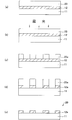
- the mask blank in which only the light shielding film is provided on the transparent substrate is described.
- the light shielding film 12 is formed from the transparent substrate side 11 to the light shielding layer 13 and the surface antireflection layer 14. May be stacked in this order.
- the light shielding film 12 may further have a three-layer structure in which a back surface antireflection layer 15 is provided between the transparent substrate 11 and the light shielding layer 13.
- the material having semi-transparency as the thin film metal silicide oxide, nitridation such as MoSi or TaSi
- the light-shielding film is a light-shielding film 12 having a structure in which a light-shielding layer 13 and a surface antireflection layer 14 are sequentially laminated from the transparent substrate 11 side.
- the light-shielding layer 13 is formed of Ta x N y .
- the surface antireflection layer 14 is made of Ta a O b .
- the manufacturing method of the light shielding film 12 is shown.
- the film formation conditions are the same as in Example 2-3, and the film composition is also the same.
- a Ta target is used on the light shielding layer 13, and the power of the DC power source is set to 0.
- a binary mask blank having a light shielding film 12 having a laminated structure of the prevention layer 14 was manufactured.
- This mask blank has an optical density of 3 or more with respect to ArF exposure light, a surface reflectance of 19.5%, and a back surface reflectance of 30.3%, and has sufficient optical characteristics as a binary mask blank. It was.
- the Ta a O b film of the surface antireflection layer 14 is originally oxidized, the altered layer caused by ArF exposure light is difficult to grow, and there is little need to adjust the film formation conditions using the relative density as an index. Is.
- this light-shielding film is a light-shielding film 12 having a structure in which a back-surface antireflection layer 15, a light-shielding layer 13, and a front-surface antireflection layer 14 are laminated in this order from the transparent substrate 11 side.
- the prevention layer (Mo a Si b Nc film Mo: Si: N 2.3 atomic%: 56.5 atomic%: 41.2 atomic%) 15 was formed with a film thickness of 12 nm.
- the film forming conditions are the same as in Example 3-2.
- This mask blank has an optical density of 3 or more with respect to ArF exposure light, a surface reflectance of 18.8%, and a back surface reflectance of 9.6%, and has sufficient optical characteristics as a binary mask blank. there were.
- the Mo e Si f O g N h film of the front antireflection layer 14 and the Mo a Si b N c film of the back antireflection layer 15 have a low Mo content and are highly oxidized or highly nitrided. The deteriorated layer caused by ArF exposure light is difficult to grow. Therefore, it is not necessary to adjust the film formation conditions using the relative density as an index.
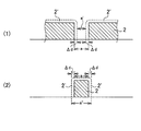
- a resist film (chemically amplified resist for electron beam drawing PRL009: manufactured by Fuji Film Electronics Materials) 23 is applied on the light shielding film 12 by spin coating.
- the light shielding film 12 includes the light shielding layer 13 and the surface antireflection layer 14.
- the resist film 23 is exposed to a desired pattern and then developed with a predetermined developer to form a resist pattern 23a.
- FIG. 4A a resist film (chemically amplified resist for electron beam drawing PRL009: manufactured by Fuji Film Electronics Materials) 23 is applied on the light shielding film 12 by spin coating.
- the light shielding film 12 includes the light shielding layer 13 and the surface antireflection layer 14.
- the resist film 23 is exposed to a desired pattern and then developed with a predetermined developer to form a resist pattern 23a.
- the light shielding film 12 is subjected to dry etching using a fluorine-based gas (CHF 3 or the like) for the surface antireflection layer 14 using the resist pattern 23a as a mask.
- the light shielding layer 13 is dry-etched using chlorine gas (Cl 2 or the like) to form a light shielding film pattern 12a.
- the remaining resist pattern is peeled off to obtain a transfer mask 20.
- the transfer mask of the present invention the relative density of the light shielding layer made of the Ta x N y film is 83.7%, and the denseness is high. Therefore, the transfer mask is durable against exposure light to which an ArF excimer laser is applied. . Therefore, the mask dimensional change is small, the lifetime is long, and high reliability can be obtained.
- a resist film (chemically amplified resist for electron beam drawing PRL009: manufactured by Fuji Film Electronics Materials) 23 is applied on the light shielding film 12 by spin coating.
- the resist film 23 is exposed to a desired pattern and then developed with a predetermined developer to form a resist pattern 23a.
- the light shielding film 12 is dry-etched using fluorine-based gas (SF 6 or the like) using the resist pattern 23a as a mask to form the light shielding film pattern 12a.
- fluorine-based gas SF 6 or the like
- the remaining resist pattern is peeled off to obtain a transfer mask 20.
- the relative density of the light shielding layer made of the Mo a Si b film is 97.6%, and since it is highly dense, it is durable against exposure light to which an ArF excimer laser is applied. . Therefore, the mask dimensional change is small, the lifetime is long, and high reliability can be obtained.
- the surface antireflection layer 14 may be made of, for example, Ta x N y (however, a highly nitrided material), Ta x O other than the above-described materials. y N z, Ta x B y O z, Ta x B y N z, Ta w B x O y N z, Ta x C y N z, Ta x C y O z, Ta w C x O y N z , etc. Is applicable.
- the above embodiment shows the light-shielding film having a structure in which the light-shielding layer 13 and the surface antireflection layer 14 are sequentially laminated from the transparent substrate 11 side.
- the present invention is not limited to this configuration.
- a light shielding film structure in which a back surface antireflection layer 15 is further provided between the transparent substrate 11 and the light shielding layer 3 may be used.
- the material of the back surface antireflection layer 15 may be selected from materials applicable to the surface antireflection layer 14.
- the materials for the front-surface antireflection layer 14 and the back-surface antireflection layer 15 may be, for example, Mo x Si y N z (however, highly nitrided). materials), Mo w Si x O y N z, Mo w Si x B y O z, Mo w Si x B y N z, Mo v Si w B x O y N z, Mo w Si x C y N z, Mo w Si x C y O z , such as Mo v Si w C x O y N z are applicable.
- the light-shielding film having a structure in which the back-surface antireflection layer 15, the light-shielding layer 13, and the front-surface antireflection layer 14 are sequentially laminated from the transparent substrate 11 side is shown.
- the present invention is not limited to this configuration.
- a light shielding film structure without the back surface antireflection layer 15 as shown in FIG. 2 may be used.
- the material of the light shielding layer 13 in this case materials containing nitrogen, for example, Mo x Si y N z, Mo w Si x B y N z, be applied like Mo w Si x C y N z preferable.
- the thin film denseness evaluation method of the present invention is a method for evaluating the thin film denseness of a mask blank having a thin film on a transparent substrate, wherein the actual density of the thin film is d1, and is calculated from the material composition of the thin film.
- Transparent substrate 11
- Light shielding film pattern 13
- Transfer mask 23 Resist film 23a Resist pattern
Landscapes
- Physics & Mathematics (AREA)
- General Physics & Mathematics (AREA)
- Preparing Plates And Mask In Photomechanical Process (AREA)
- Physical Vapour Deposition (AREA)
Priority Applications (3)
| Application Number | Priority Date | Filing Date | Title |
|---|---|---|---|
| KR1020117027174A KR101702682B1 (ko) | 2009-04-16 | 2010-04-09 | 마스크 블랭크 및 전사용 마스크 |
| US13/264,664 US8709681B2 (en) | 2009-04-16 | 2010-04-09 | Mask blank, transfer mask, and film denseness evaluation method |
| JP2011509271A JPWO2010119811A1 (ja) | 2009-04-16 | 2010-04-09 | マスクブランク及び転写用マスク並びに膜緻密性評価方法 |
Applications Claiming Priority (2)
| Application Number | Priority Date | Filing Date | Title |
|---|---|---|---|
| JP2009100050 | 2009-04-16 | ||
| JP2009-100050 | 2009-04-16 |
Publications (1)
| Publication Number | Publication Date |
|---|---|
| WO2010119811A1 true WO2010119811A1 (ja) | 2010-10-21 |
Family
ID=42982473
Family Applications (1)
| Application Number | Title | Priority Date | Filing Date |
|---|---|---|---|
| PCT/JP2010/056409 Ceased WO2010119811A1 (ja) | 2009-04-16 | 2010-04-09 | マスクブランク及び転写用マスク並びに膜緻密性評価方法 |
Country Status (5)
| Country | Link |
|---|---|
| US (1) | US8709681B2 (enExample) |
| JP (2) | JPWO2010119811A1 (enExample) |
| KR (1) | KR101702682B1 (enExample) |
| TW (1) | TWI444760B (enExample) |
| WO (1) | WO2010119811A1 (enExample) |
Cited By (1)
| Publication number | Priority date | Publication date | Assignee | Title |
|---|---|---|---|---|
| JP2020173333A (ja) * | 2019-04-10 | 2020-10-22 | デクセリアルズ株式会社 | 光学素子用薄膜及びその製造方法、無機偏光板及びその製造方法、並びに光学素子及び光学機器 |
Families Citing this family (5)
| Publication number | Priority date | Publication date | Assignee | Title |
|---|---|---|---|---|
| US20130160948A1 (en) * | 2011-12-23 | 2013-06-27 | Lam Research Corporation | Plasma Processing Devices With Corrosion Resistant Components |
| JP6335735B2 (ja) * | 2014-09-29 | 2018-05-30 | Hoya株式会社 | フォトマスク及び表示装置の製造方法 |
| JP6489951B2 (ja) * | 2015-06-12 | 2019-03-27 | 東芝メモリ株式会社 | 半導体装置の製造方法 |
| JP6932552B2 (ja) * | 2017-05-31 | 2021-09-08 | Hoya株式会社 | マスクブランク、転写用マスクの製造方法及び半導体デバイスの製造方法 |
| JP2022045198A (ja) * | 2020-09-08 | 2022-03-18 | 凸版印刷株式会社 | 位相シフトマスクブランク、位相シフトマスク及び位相シフトマスクの製造方法 |
Citations (2)
| Publication number | Priority date | Publication date | Assignee | Title |
|---|---|---|---|---|
| JP2001312043A (ja) * | 2000-04-27 | 2001-11-09 | Dainippon Printing Co Ltd | ハーフトーン位相シフトフォトマスク及びハーフトーン位相シフトフォトマスク用ブランクス |
| WO2008139904A1 (ja) * | 2007-04-27 | 2008-11-20 | Hoya Corporation | フォトマスクブランク及びフォトマスク |
Family Cites Families (15)
| Publication number | Priority date | Publication date | Assignee | Title |
|---|---|---|---|---|
| JPH0690508B2 (ja) * | 1987-06-30 | 1994-11-14 | 三菱電機株式会社 | フオトマスク |
| US5919321A (en) * | 1996-08-13 | 1999-07-06 | Hitachi Metals, Ltd. | Target material of metal silicide |
| JP3608654B2 (ja) * | 2000-09-12 | 2005-01-12 | Hoya株式会社 | 位相シフトマスクブランク、位相シフトマスク |
| JP2002156742A (ja) | 2000-11-20 | 2002-05-31 | Shin Etsu Chem Co Ltd | 位相シフトマスクブランク、位相シフトマスク及びこれらの製造方法 |
| JP2002169265A (ja) | 2000-12-01 | 2002-06-14 | Hoya Corp | フォトマスクブランクス及びフォトマスクブランクスの製造方法 |
| WO2003031673A1 (en) * | 2001-10-02 | 2003-04-17 | Advanced Systems Of Technology Incubation | Thin metal oxide film and process for producing the same |
| JP4158885B2 (ja) * | 2002-04-22 | 2008-10-01 | Hoya株式会社 | フォトマスクブランクの製造方法 |
| JP4534417B2 (ja) * | 2002-12-13 | 2010-09-01 | ソニー株式会社 | スパッタターゲットの製造方法 |
| JP2005156700A (ja) | 2003-11-21 | 2005-06-16 | Shin Etsu Chem Co Ltd | 位相シフトマスクブランク、位相シフトマスク、位相シフトマスクブランクの製造方法、及びパターン転写方法 |
| JP2006078825A (ja) | 2004-09-10 | 2006-03-23 | Shin Etsu Chem Co Ltd | フォトマスクブランクおよびフォトマスクならびにこれらの製造方法 |
| JP5105217B2 (ja) * | 2005-04-25 | 2012-12-26 | 大日本印刷株式会社 | 金属積層体 |
| JP4766518B2 (ja) * | 2006-03-31 | 2011-09-07 | Hoya株式会社 | マスクブランク及びフォトマスク |
| TWI444757B (zh) * | 2006-04-21 | 2014-07-11 | Asahi Glass Co Ltd | 用於極紫外光(euv)微影術之反射性空白光罩 |
| JP2008101246A (ja) * | 2006-10-19 | 2008-05-01 | Asahi Glass Co Ltd | Euvリソグラフィ用反射型マスクブランクを製造する際に使用されるスパッタリングターゲット |
| KR101471358B1 (ko) * | 2007-03-12 | 2014-12-10 | 주식회사 에스앤에스텍 | 하프톤형 위상반전 블랭크 마스크, 하프톤형 위상반전포토마스크 및 그의 제조방법 |
-
2010
- 2010-04-09 JP JP2011509271A patent/JPWO2010119811A1/ja active Pending
- 2010-04-09 US US13/264,664 patent/US8709681B2/en active Active
- 2010-04-09 KR KR1020117027174A patent/KR101702682B1/ko active Active
- 2010-04-09 WO PCT/JP2010/056409 patent/WO2010119811A1/ja not_active Ceased
- 2010-04-15 TW TW99111731A patent/TWI444760B/zh active
-
2015
- 2015-01-21 JP JP2015009267A patent/JP5899558B2/ja active Active
Patent Citations (2)
| Publication number | Priority date | Publication date | Assignee | Title |
|---|---|---|---|---|
| JP2001312043A (ja) * | 2000-04-27 | 2001-11-09 | Dainippon Printing Co Ltd | ハーフトーン位相シフトフォトマスク及びハーフトーン位相シフトフォトマスク用ブランクス |
| WO2008139904A1 (ja) * | 2007-04-27 | 2008-11-20 | Hoya Corporation | フォトマスクブランク及びフォトマスク |
Cited By (4)
| Publication number | Priority date | Publication date | Assignee | Title |
|---|---|---|---|---|
| JP2020173333A (ja) * | 2019-04-10 | 2020-10-22 | デクセリアルズ株式会社 | 光学素子用薄膜及びその製造方法、無機偏光板及びその製造方法、並びに光学素子及び光学機器 |
| CN111812764A (zh) * | 2019-04-10 | 2020-10-23 | 迪睿合株式会社 | 光学元件用薄膜及其制造方法、无机偏振片及其制造方法、以及光学元件和光学仪器 |
| JP7332324B2 (ja) | 2019-04-10 | 2023-08-23 | デクセリアルズ株式会社 | 無機偏光板及びその製造方法、並びに光学機器 |
| CN111812764B (zh) * | 2019-04-10 | 2024-02-06 | 迪睿合株式会社 | 光学元件用薄膜及其制造方法、无机偏振片及其制造方法 |
Also Published As
| Publication number | Publication date |
|---|---|
| TW201109833A (en) | 2011-03-16 |
| JP2015096973A (ja) | 2015-05-21 |
| JP5899558B2 (ja) | 2016-04-06 |
| KR101702682B1 (ko) | 2017-02-06 |
| JPWO2010119811A1 (ja) | 2012-10-22 |
| KR20120057569A (ko) | 2012-06-05 |
| US8709681B2 (en) | 2014-04-29 |
| TWI444760B (zh) | 2014-07-11 |
| US20120034434A1 (en) | 2012-02-09 |
Similar Documents
| Publication | Publication Date | Title |
|---|---|---|
| TWI436161B (zh) | 遮罩基底及轉印用遮罩之製造方法 | |
| KR101450947B1 (ko) | 포토마스크 블랭크 및 포토마스크 그리고 포토마스크의 제조 방법 | |
| JP6133530B1 (ja) | マスクブランク、位相シフトマスクおよび半導体デバイスの製造方法 | |
| US8354205B2 (en) | Mask blank, transfer mask, and methods of manufacturing the same | |
| JP6500791B2 (ja) | ハーフトーン位相シフト型フォトマスクブランク及びその製造方法 | |
| JP5899558B2 (ja) | マスクブランク及び転写用マスク | |
| TW201921097A (zh) | 空白光罩及光罩 | |
| CN106019809B (zh) | 半色调相移掩模坯,半色调相移掩模,和图案曝光方法 | |
| JP7106492B2 (ja) | マスクブランク、位相シフトマスクおよび半導体デバイスの製造方法 | |
| JP2020034666A5 (enExample) | ||
| WO2010050447A1 (ja) | フォトマスクブランク、フォトマスク及びその製造方法 | |
| JP2020052195A (ja) | 位相シフト型フォトマスクブランク及び位相シフト型フォトマスク | |
| JP2018116269A (ja) | 表示装置製造用の位相シフトマスクブランク、表示装置製造用の位相シフトマスクの製造方法、並びに表示装置の製造方法 | |
| WO2011030521A1 (ja) | マスクブランクの製造方法、転写用マスクの製造方法および反射型マスクの製造方法 | |
| JP6542497B1 (ja) | マスクブランク、位相シフトマスク及び半導体デバイスの製造方法 | |
| TWI788304B (zh) | 半色調相移型空白光罩、其製造方法及半色調相移型光罩 | |
| JP2004085760A (ja) | ハーフトーン型位相シフトマスク用ブランク及びそれを用いたハーフトーン型位相シフトマスク、並びにパターン転写法 | |
| JP5217345B2 (ja) | フォトマスクおよびフォトマスクブランクス | |
| KR20180109697A (ko) | 위상 시프트 마스크 블랭크 및 그것을 사용한 위상 시프트 마스크의 제조 방법, 그리고 패턴 전사 방법 | |
| TWI809232B (zh) | 遮罩基底、相移遮罩、相移遮罩之製造方法及半導體元件之製造方法 | |
| JP7553735B1 (ja) | 反射型フォトマスクブランク、反射型フォトマスク及び反射型フォトマスクの製造方法 | |
| JP7618677B2 (ja) | マスクブランク、位相シフトマスク、位相シフトマスクの製造方法及び半導体デバイスの製造方法 | |
| EP4474906A1 (en) | Phase shift mask and method for manufacturing phase shift mask | |
| CN117916660A (zh) | 掩模坯料、相移掩模及半导体器件的制造方法 |
Legal Events
| Date | Code | Title | Description |
|---|---|---|---|
| 121 | Ep: the epo has been informed by wipo that ep was designated in this application |
Ref document number: 10764395 Country of ref document: EP Kind code of ref document: A1 |
|
| WWE | Wipo information: entry into national phase |
Ref document number: 2011509271 Country of ref document: JP |
|
| WWE | Wipo information: entry into national phase |
Ref document number: 13264664 Country of ref document: US |
|
| NENP | Non-entry into the national phase |
Ref country code: DE |
|
| ENP | Entry into the national phase |
Ref document number: 20117027174 Country of ref document: KR Kind code of ref document: A |
|
| 122 | Ep: pct application non-entry in european phase |
Ref document number: 10764395 Country of ref document: EP Kind code of ref document: A1 |