WO2010116802A1 - 圧電素子 - Google Patents
圧電素子 Download PDFInfo
- Publication number
- WO2010116802A1 WO2010116802A1 PCT/JP2010/052697 JP2010052697W WO2010116802A1 WO 2010116802 A1 WO2010116802 A1 WO 2010116802A1 JP 2010052697 W JP2010052697 W JP 2010052697W WO 2010116802 A1 WO2010116802 A1 WO 2010116802A1
- Authority
- WO
- WIPO (PCT)
- Prior art keywords
- layer
- elastic modulus
- piezoelectric
- substrate
- piezoelectric element
- Prior art date
- Legal status (The legal status is an assumption and is not a legal conclusion. Google has not performed a legal analysis and makes no representation as to the accuracy of the status listed.)
- Ceased
Links
Images




Classifications
-
- C—CHEMISTRY; METALLURGY
- C23—COATING METALLIC MATERIAL; COATING MATERIAL WITH METALLIC MATERIAL; CHEMICAL SURFACE TREATMENT; DIFFUSION TREATMENT OF METALLIC MATERIAL; COATING BY VACUUM EVAPORATION, BY SPUTTERING, BY ION IMPLANTATION OR BY CHEMICAL VAPOUR DEPOSITION, IN GENERAL; INHIBITING CORROSION OF METALLIC MATERIAL OR INCRUSTATION IN GENERAL
- C23C—COATING METALLIC MATERIAL; COATING MATERIAL WITH METALLIC MATERIAL; SURFACE TREATMENT OF METALLIC MATERIAL BY DIFFUSION INTO THE SURFACE, BY CHEMICAL CONVERSION OR SUBSTITUTION; COATING BY VACUUM EVAPORATION, BY SPUTTERING, BY ION IMPLANTATION OR BY CHEMICAL VAPOUR DEPOSITION, IN GENERAL
- C23C24/00—Coating starting from inorganic powder
- C23C24/02—Coating starting from inorganic powder by application of pressure only
- C23C24/04—Impact or kinetic deposition of particles
-
- C—CHEMISTRY; METALLURGY
- C23—COATING METALLIC MATERIAL; COATING MATERIAL WITH METALLIC MATERIAL; CHEMICAL SURFACE TREATMENT; DIFFUSION TREATMENT OF METALLIC MATERIAL; COATING BY VACUUM EVAPORATION, BY SPUTTERING, BY ION IMPLANTATION OR BY CHEMICAL VAPOUR DEPOSITION, IN GENERAL; INHIBITING CORROSION OF METALLIC MATERIAL OR INCRUSTATION IN GENERAL
- C23C—COATING METALLIC MATERIAL; COATING MATERIAL WITH METALLIC MATERIAL; SURFACE TREATMENT OF METALLIC MATERIAL BY DIFFUSION INTO THE SURFACE, BY CHEMICAL CONVERSION OR SUBSTITUTION; COATING BY VACUUM EVAPORATION, BY SPUTTERING, BY ION IMPLANTATION OR BY CHEMICAL VAPOUR DEPOSITION, IN GENERAL
- C23C28/00—Coating for obtaining at least two superposed coatings either by methods not provided for in a single one of groups C23C2/00 - C23C26/00 or by combinations of methods provided for in subclasses C23C and C25C or C25D
- C23C28/04—Coating for obtaining at least two superposed coatings either by methods not provided for in a single one of groups C23C2/00 - C23C26/00 or by combinations of methods provided for in subclasses C23C and C25C or C25D only coatings of inorganic non-metallic material
- C23C28/042—Coating for obtaining at least two superposed coatings either by methods not provided for in a single one of groups C23C2/00 - C23C26/00 or by combinations of methods provided for in subclasses C23C and C25C or C25D only coatings of inorganic non-metallic material including a refractory ceramic layer, e.g. refractory metal oxides, ZrO2, rare earth oxides
-
- C—CHEMISTRY; METALLURGY
- C23—COATING METALLIC MATERIAL; COATING MATERIAL WITH METALLIC MATERIAL; CHEMICAL SURFACE TREATMENT; DIFFUSION TREATMENT OF METALLIC MATERIAL; COATING BY VACUUM EVAPORATION, BY SPUTTERING, BY ION IMPLANTATION OR BY CHEMICAL VAPOUR DEPOSITION, IN GENERAL; INHIBITING CORROSION OF METALLIC MATERIAL OR INCRUSTATION IN GENERAL
- C23C—COATING METALLIC MATERIAL; COATING MATERIAL WITH METALLIC MATERIAL; SURFACE TREATMENT OF METALLIC MATERIAL BY DIFFUSION INTO THE SURFACE, BY CHEMICAL CONVERSION OR SUBSTITUTION; COATING BY VACUUM EVAPORATION, BY SPUTTERING, BY ION IMPLANTATION OR BY CHEMICAL VAPOUR DEPOSITION, IN GENERAL
- C23C28/00—Coating for obtaining at least two superposed coatings either by methods not provided for in a single one of groups C23C2/00 - C23C26/00 or by combinations of methods provided for in subclasses C23C and C25C or C25D
- C23C28/04—Coating for obtaining at least two superposed coatings either by methods not provided for in a single one of groups C23C2/00 - C23C26/00 or by combinations of methods provided for in subclasses C23C and C25C or C25D only coatings of inorganic non-metallic material
- C23C28/048—Coating for obtaining at least two superposed coatings either by methods not provided for in a single one of groups C23C2/00 - C23C26/00 or by combinations of methods provided for in subclasses C23C and C25C or C25D only coatings of inorganic non-metallic material with layers graded in composition or physical properties
-
- H—ELECTRICITY
- H10—SEMICONDUCTOR DEVICES; ELECTRIC SOLID-STATE DEVICES NOT OTHERWISE PROVIDED FOR
- H10N—ELECTRIC SOLID-STATE DEVICES NOT OTHERWISE PROVIDED FOR
- H10N30/00—Piezoelectric or electrostrictive devices
- H10N30/01—Manufacture or treatment
- H10N30/07—Forming of piezoelectric or electrostrictive parts or bodies on an electrical element or another base
- H10N30/074—Forming of piezoelectric or electrostrictive parts or bodies on an electrical element or another base by depositing piezoelectric or electrostrictive layers, e.g. aerosol or screen printing
-
- H—ELECTRICITY
- H10—SEMICONDUCTOR DEVICES; ELECTRIC SOLID-STATE DEVICES NOT OTHERWISE PROVIDED FOR
- H10N—ELECTRIC SOLID-STATE DEVICES NOT OTHERWISE PROVIDED FOR
- H10N30/00—Piezoelectric or electrostrictive devices
- H10N30/01—Manufacture or treatment
- H10N30/07—Forming of piezoelectric or electrostrictive parts or bodies on an electrical element or another base
- H10N30/074—Forming of piezoelectric or electrostrictive parts or bodies on an electrical element or another base by depositing piezoelectric or electrostrictive layers, e.g. aerosol or screen printing
- H10N30/079—Forming of piezoelectric or electrostrictive parts or bodies on an electrical element or another base by depositing piezoelectric or electrostrictive layers, e.g. aerosol or screen printing using intermediate layers, e.g. for growth control
-
- H—ELECTRICITY
- H10—SEMICONDUCTOR DEVICES; ELECTRIC SOLID-STATE DEVICES NOT OTHERWISE PROVIDED FOR
- H10N—ELECTRIC SOLID-STATE DEVICES NOT OTHERWISE PROVIDED FOR
- H10N30/00—Piezoelectric or electrostrictive devices
- H10N30/704—Piezoelectric or electrostrictive devices based on piezoelectric or electrostrictive films or coatings
- H10N30/706—Piezoelectric or electrostrictive devices based on piezoelectric or electrostrictive films or coatings characterised by the underlying bases, e.g. substrates
- H10N30/708—Intermediate layers, e.g. barrier, adhesion or growth control buffer layers
Definitions
- the present invention relates to a piezoelectric element having a thin film formed by an aerosol deposition method as a piezoelectric film.
- the aerosol deposition method has attracted attention as a method for forming a piezoelectric film in a piezoelectric actuator used in an inkjet printer or the like.
- an aerosol composed of ceramic fine particles dispersed in a gas is sprayed from a nozzle and sprayed onto the substrate surface at a high speed to pulverize and deposit the fine particles on the substrate to form a ceramic thin film.
- It is a membrane method.
- This method uses the normal temperature impact solidification phenomenon caused by the induction of the mechanochemical reaction caused by the release of the local impact energy generated by the collision of ceramic fine particles with the substrate surface. Is a film formation technique that acts as a reaction energy during film formation.
- the annealing treatment is intended to improve the piezoelectric characteristics and the like of the thin film by heating the thin film formed by the aerosol deposition method and growing crystal grains inside the thin film. It is known that Fe and Cr in stainless steel are diffused into the piezoelectric layer by this annealing treatment, and the piezoelectric characteristics are deteriorated. In order to prevent this, the above-mentioned diffusion is prevented by providing a diffusion prevention layer made of an insulating ceramic material, a metal material, a conductive oxide, etc. between the stainless steel substrate and the piezoelectric layer. It is proposed in Document 1.
- An object of the present invention is to provide a piezoelectric element that can suppress the occurrence of film peeling and short circuit and can improve the piezoelectric characteristics.
- a piezoelectric element is a piezoelectric element having a three-layer structure in which a substrate, a single diffusion prevention layer, and a piezoelectric layer are laminated in this order,
- Each of the prevention layer and the piezoelectric layer is a film formed by an aerosol deposition method, and the elastic modulus of the diffusion prevention layer is less than the elastic modulus of the substrate and more than the elastic modulus of the piezoelectric layer. It is characterized by that.
- the piezoelectric element according to the first aspect wherein the diffusion preventing layer is made of material particles having a smaller elastic modulus as the film thickness by the aerosol deposition method is larger.
- a piezoelectric element according to a third invention is characterized in that, in the first or second invention, the diffusion preventing layer is made of zirconia to which alumina is added.
- a piezoelectric element according to a fourth invention is characterized in that, in the first or second invention, the diffusion preventing layer is composed of lead zirconate titanate.
- a piezoelectric element of a fifth invention is characterized in that, in the first or second invention, the diffusion preventing layer is made of zirconia having a thickness of 5 ⁇ m or more.
- the elastic modulus of the substrate ⁇ the elastic modulus of the diffusion preventing layer ⁇ the elastic modulus of the piezoelectric film, so that the elastic modulus gap between the films in the multilayer piezoelectric element is reduced. Can do. Therefore, it is possible to suppress the occurrence of film peeling or short circuit and improve the piezoelectric characteristics.
- the film forming apparatus shown in FIG. 1 includes an aerosol generator 1 for generating aerosol by dispersing material particles in a carrier gas, and an internal structure. And a chamber 2 for carrying out the membrane.
- the aerosol generator 1 stores a predetermined amount of material particles (for example, particles having a particle size of about 0.5 ⁇ m to 5.0 ⁇ m) and introduces a carrier gas.
- the aerosol generator 1 generates a winding gas when the carrier gas is introduced. Further, the aerosol generator 1 applies vibration to the material particles from the lower part by an ultrasonic vibration apparatus or a flow stirring using a part of the carrier gas. As a result, the material particles are dispersed in the carrier gas, and aerosol is generated.
- the carrier gas for example, an inert gas such as helium or argon, nitrogen, air, oxygen, or the like can be used.
- One end of an aerosol supply pipe 3 is inserted in the upper part of the aerosol generator 1.
- the other end of the aerosol supply pipe 3 is disposed inside the chamber 2 and is connected to an injection nozzle 4.
- the chamber 2 is connected with a mechanical booster pump and a rotary pump, and these pumps depressurize the inside of the chamber 2. As a result, the internal pressure of the chamber 2 becomes lower than the internal pressure of the aerosol generator 1. Due to the differential pressure between the chamber 2 and the aerosol generator 1, the aerosol generated in the aerosol generator 1 is sucked into the aerosol supply pipe 3 and supplied to the injection nozzle 4.
- the cavity inside the injection nozzle 4 has such a shape that the cross-sectional area decreases as it travels inside.
- the aerosol that has entered the inside of the injection nozzle 4 from the introduction opening of the injection nozzle 4 is accelerated and sprayed from the injection opening of the injection nozzle 4 onto the substrate 7 as an aerosol flow 5 at a high speed.
- the material particles that collide with the surface of the substrate 7 are crushed and deposited to form a thin film.
- a substrate holder 6 for mounting the substrate 7 on the lower surface is disposed above the injection opening of the injection nozzle 4.
- the substrate holder 6 has a rectangular plate shape.
- the substrate holder 6 is suspended from the ceiling of the chamber 2 in a horizontal posture by the driving device 8.
- the driving device 8 drives the substrate holder 6 in the left-right direction in FIG. By this driving in the left-right direction, scanning film formation on the substrate 7 is performed. By this scanning film formation, a thin film is formed in a predetermined wide range of the substrate 7.
- the substrate 7 that is a film formation target includes a stainless steel substrate, but is not limited thereto, and may be a substrate composed of other metals, silicon, semiconductor, resin, or the like.
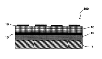
- the piezoelectric element 100 shown in FIG. 2 is an example of a form used as a piezoelectric actuator.
- a single diffusion prevention layer 12 that is not a plurality of layers is laminated on a substrate 7.
- a lower electrode 15 is formed on the diffusion prevention layer 12.
- a piezoelectric layer 13 made of a piezoelectric material that contributes to deformation of the piezoelectric actuator is laminated on the lower electrode 15.
- An upper electrode 16 is laminated on the piezoelectric layer 13.
- the piezoelectric element 100 has a three-layer structure in which the substrate 7, the diffusion prevention layer 12 and the piezoelectric layer 13 are laminated, and the lower electrode 15 is formed between the diffusion prevention layer 12 and the piezoelectric layer 13. In addition, an upper electrode 16 is formed on the piezoelectric layer 13.
- the diffusion prevention layer 12 and the piezoelectric layer 13 are respectively formed on the substrate 7 by the aerosol deposition method described above.
- the lower electrode 15 is provided over the entire surface of the diffusion prevention layer 12 at the interface between the diffusion prevention layer 12 and the piezoelectric layer 13.
- the lower electrode 15 is used as a ground electrode that is grounded and always has a ground potential.
- the upper electrode 16 is configured as an electrode pattern on the upper surface of the piezoelectric layer 13 by a plurality of independent regions.
- the upper electrode 16 has a lead portion connected to each individual region, and is connected to the drive circuit IC via the lead portion.
- the upper electrode 16 is used as a drive electrode to which a ground potential or a potential different from the ground potential is selectively applied by the drive circuit IC.
- the lower electrode 15 and the upper electrode 16 are made of a metal such as Au or Pt, for example.
- the feature of the piezoelectric element 100 of this embodiment is that the elastic modulus value of the substrate 7 is configured to be equal to or larger than the elastic modulus value of the diffusion prevention layer 12. Further, the elastic modulus of the diffusion preventing layer 12 is configured to be equal to or greater than the elastic modulus of the piezoelectric layer 13. By setting it as this structure, the elastic-modulus gap between each layer can be made small.
- the elastic modulus of each film can be measured by a nanoindentation method. Specifically, it is a value measured using an ultra-fine indentation hardness tester: ENT-1100a manufactured by Elionix Co., with an indentation load of 5 mN.
- the elastic modulus here is a value measured after forming each layer and before annealing.
- the piezoelectric characteristics were evaluated by calculating the value of the piezoelectric constant -d31 indicating the ease of deformation in the thickness direction on the electrode surface when a voltage was applied.
- This piezoelectric constant ⁇ d31 can be calculated by an operation such as measuring the displacement of the piezoelectric actuator.
- the diffusion prevention layer 12 is formed on the surface of the substrate 7 by the above-described aerosol deposition method.
- material particles having a smaller elastic modulus as the deposition thickness by the aerosol deposition method is thicker are used as the material constituting the material particles when the diffusion prevention layer 12 is formed.
- the detailed material configuration of the material particles will be described later.
- the elastic modulus of the diffusion preventing layer 12 is set by the aerosol deposition method so as to be equal to or lower than that of the substrate 7 and equal to or higher than that of the piezoelectric layer 13. It can be easily done by adjusting the thickness at the time.
- the powder on the surface is removed, and the lower electrode 15 is formed on the surface of the diffusion preventing layer 12 by vapor deposition or sputtering, or by applying and drying a paste containing metal particles. Film.
- a stress release annealing process is performed by heating at a relatively low temperature (about 500 ° C.). The stress release annealing treatment is performed for the purpose of heating the thin film formed by the aerosol deposition method to remove the film forming gas and moisture mixed in the film and releasing the residual stress of the thin film. .
- the piezoelectric layer 13 is again formed on the surface of the lower electrode 15 by the aerosol deposition method.
- material particles for forming the piezoelectric layer 13 piezoelectric materials such as barium titanate, lead titanate, lead magnesium niobate, lead nickel niobate, lead zinc niobate and the like can be used.
- a grain growth annealing process is performed by heating at a relatively high temperature (about 800 to 900 ° C.) in order to remove the powder on the surface and grow crystal grains of the piezoelectric layer. .
- the grain growth annealing treatment is intended to improve crystal characteristics of the thin film by heating the piezoelectric layer 13 formed by the aerosol deposition method to achieve growth of crystal grains in the thin film and correction of lattice defects. It is a process performed in.
- the piezoelectric layer 13 formed by the aerosol deposition method has a large change in elastic modulus in the vicinity of the interface due to the grain growth annealing process.
- problems such as film peeling can be avoided by employing the layer configuration of the present embodiment having the above-described elastic modulus relationship.
- the upper electrode 16 is formed on the surface of the piezoelectric layer 13.
- masking is performed and a vapor deposition method or a sputtering method is performed.
- a metal layer may be formed on the entire surface of the piezoelectric layer 13 by vapor deposition or sputtering, and then formed into a predetermined pattern using photolithography etching.
- the upper electrode 16 may be formed by screen printing directly on the surface of the piezoelectric layer 13.
- the piezoelectric element 100 according to the present embodiment is completed.
- the piezoelectric element 100 has a three-layer structure including the substrate 7, the diffusion prevention layer 12, and the piezoelectric layer 13 except for the upper electrode 16 and the lower electrode 15. Constitute. Furthermore, their elastic modulus is The elastic modulus of the substrate 7 ⁇ the elastic modulus of the diffusion preventing layer 12 ⁇ the elastic modulus of the piezoelectric layer 13 is configured. The reason for this configuration is to reduce the elastic modulus gap between the films.
- the diffusion prevention layer 12 when the diffusion prevention layer 12 is provided by the aerosol deposition method as described above, the elastic modulus gap existing between the piezoelectric layer 13 and the diffusion prevention layer 12 and the elastic modulus obtained by the grain growth annealing process described above. Due to the large fluctuation, the inter-membrane stress rapidly increases between the piezoelectric layer 13 and the diffusion preventing layer 12. As a result, after performing the grain growth annealing treatment, film peeling may easily occur at the film interface between the piezoelectric layer 13 and the diffusion prevention layer 12.
- the elastic modulus of the substrate 7 ⁇ the elastic modulus of the diffusion preventing layer 12 ⁇ the elastic modulus of the piezoelectric film 13 is set.
- the elastic modulus gap between the films in the piezoelectric element 100 can be reduced. Therefore, it is possible to reduce the stress generated between the layers and make it difficult to generate the interface peeling of the piezoelectric layer 13. Accordingly, the occurrence of film peeling can be suppressed and the yield can be improved. In addition, cracks and pinholes are hardly formed, and occurrence of a short circuit can be suppressed. Further, the piezoelectric characteristics of the piezoelectric element 100 can be improved by reducing the internal stress of the piezoelectric layer 13.
- each embodiment (3-A) First embodiment and second embodiment stainless steel is provided as a substrate, and alumina is used as a diffusion preventing layer between the piezoelectric layer composed of lead zirconate titanate.
- the elastic modulus of the substrate is about 260 [GPa]
- the elastic modulus of the diffusion prevention layer is about 390 [GPa]
- the elastic modulus of the piezoelectric layer is about 120 [GPa]. Since the elastic modulus protrudes and is large, the elastic modulus gap between the films becomes very large.
- the diffusion prevention layer 12 is composed of zirconia to which alumina is added so as to exhibit intermediate characteristics between alumina and zirconia.
- the elastic modulus values of the substrate 7 and the diffusion prevention layer 12 are about 260 [GPa], respectively, and the elastic modulus of the piezoelectric layer 13 is 115. It was found that the difference between the elastic modulus of the diffusion preventing layer 12 and the elastic modulus of the substrate 7 and the piezoelectric layer 13 can be reduced.
- the diffusion prevention layer 12 by forming the diffusion prevention layer 12 using zirconia to which alumina is added, it is possible to reliably reduce the elastic modulus gap between the films in the multilayer piezoelectric element 100 and to remove the film. Generation
- production of a short circuit can be suppressed.
- the diffusion prevention layer 12 is composed of lead zirconate titanate.
- the value of the elastic modulus of the diffusion preventing layer 12 is about 160 [GPa]
- the elastic modulus of the piezoelectric layer 13 is 70 [GPa].
- the value of the elastic modulus of the substrate 7 is about 260 [GPa].
- the gap in elastic modulus between the films in the multilayer piezoelectric element 100 is reliably reduced, and film peeling or short-circuiting occurs.
- production can be suppressed and generation
- the inventors of the present application examined the relationship between the diffusion preventing effect of zirconia used as the diffusion preventing layer 12 and the film thickness, and obtained the results shown in FIG.
- FIG. 3 it can be seen that Fe and Cr contained in the stainless steel substrate of the substrate 7 are diffused into the diffusion preventing layer 12. However, it can be seen that the diffusion of Fe and Cr is almost completed at a distance of about 1 ⁇ m in the thickness direction after entering the diffusion preventing layer 12 from the substrate 7. In other words, as long as the function as the diffusion preventing layer 12 is obtained, it is found that the thickness of the zirconia layer is sufficient to be about 1 ⁇ m to 2 ⁇ m at most, and it does not make much sense to increase the thickness further.
- Pt is a component element of the lower electrode 15 and is used to confirm the baseline of composition analysis and the presence or absence of diffusion into the piezoelectric layer 13.
- the value of the elastic modulus is about 270 [GPa] when the film thickness of zirconia is about 1.6 ⁇ m. Thereafter, the value of the elastic modulus decreases as the film thickness increases, and the film thickness is about 5 ⁇ m.
- the value of the elastic modulus is about 230 [GPa], and when the film thickness is about 10 ⁇ m, the value of the elastic modulus decreases to about 200 [GPa], which is equal to or less than the standard bulk property of zirconia. After this, even when the film thickness increased, the elastic modulus did not decrease so much, and when the film thickness was about 25 ⁇ m, the value of the elastic modulus was about 190 [GPa].
- a zirconia film thickness of about 1 ⁇ m to 2 ⁇ m is sufficient to obtain the effect as the diffusion preventing layer 12, but there is room for controlling the elastic modulus value to a desired value by further increasing the thickness. . It was found that an effect of reducing the elastic modulus can be obtained by increasing the zirconia film thickness to at least about 5 ⁇ m.
- the diffusion prevention layer 12 is composed of zirconia having a thickness of 5 ⁇ m or more.
- the diffusion prevention layer 12 is made of zirconia and has a film thickness of 5 ⁇ m or more, thereby reliably reducing the elastic modulus gap between the films in the multilayer piezoelectric element 100.
- membrane peeling and a short circuit can be suppressed.
- the elastic modulus itself of the piezoelectric layer 13 is lowered, it is possible to further prevent film peeling and short circuit.
- Example 1 Preparation of Substrate A diffusion bonded SUS substrate (head) and an evaluation SUS substrate (elastic modulus measurement) having a width of 15 mm, a depth of 35 mm, and a thickness of 0.4 mm were prepared. Using a nanoindenter, the elastic modulus of the evaluation SUS substrate was measured at a load of 5 mN. The elastic modulus values are shown in FIG.
- Diffusion Prevention Layer A ZrO 2 (20% Al 2 O 3 added) film is formed as a diffusion prevention layer 12 on these substrates using a film deposition apparatus based on the aerosol deposition method based on the above-described embodiment. did.
- the aerosol generator 1 was charged with 160 g of ZrO 2 (20% Al 2 O 3 added) powder (TZ-3YS20A manufactured by Tosoh Corporation).
- the SUS substrate 7 was set on the substrate holder 6 and the portions other than the film formation range were attached with tape.
- the substrate holder 6 was set on the XY stage of the driving device 8 in the chamber 2 and a reciprocating scan was started.
- the stage was moved in such a manner that two rows (two sheets) of film formation could be performed in the same batch. That is, the two substrates 7 and 7 are arranged in parallel so as to face the ejection direction of the nozzle 4.
- (a) the nozzle 4 was brought close to one substrate 7 and faced.
- the nozzle 4 was moved to the other substrate 7 side substantially at right angles to the jetting direction and opposed to the other substrate 7. Thereafter, (c) it was moved away from the other substrate 7 once. After that, (d) the nozzle 4 was again brought close to the other substrate 7 to face it. (E) The nozzle 4 was moved to the one substrate 7 side substantially at right angles to the ejection direction, and was made to face the one substrate 7. Thereafter, (f) the substrate was moved away from the one substrate 7. Thereafter, the XY stage of the driving device 8 was moved so as to repeat the movements (a) to (f). The chamber 2 was evacuated to an ultimate vacuum pressure of 10 to 20 Pa.
- Carrier gas was introduced from three systems (flow, crushing, acceleration), and the raw material powder was fluidly stirred.
- the total flow rate of the carrier gas (the total of the three systems) was adjusted to a predetermined total flow rate, and the flow gas flow rate was set to a constant flow rate while observing the flow state.
- the aerosol concentration was adjusted to a desired concentration by changing the ratio of the crushing gas and the acceleration gas.
- spray injection 5 min outside the film formation range
- aerosol was sprayed onto each SUS substrate for a predetermined film formation time. After the predetermined film formation time was completed, the film formation gas was stopped and the film formation chamber was opened in vacuum.
- the substrate holder was removed from the XY stage to obtain the SUS substrate 7 on which the diffusion preventing layer 12 was formed.
- the surface of the SUS substrate 7 on which the diffusion prevention layer 12 was formed was air blown to remove the adhered powder.
- the film thickness of the diffusion preventing layer 12 on the SUS substrate 7 was measured using a step gauge, it was 0.91 to 2.91 ⁇ m.
- the elastic modulus of the diffusion prevention layer 12 on the evaluation SUS substrate was measured using a nanoindenter at a load of 5 mN. The elastic modulus values are shown in FIG.
- Piezoelectric Layer A PZT film was formed as the piezoelectric layer 13 on each laminated body after the stress release annealing treatment by the same aerosol deposition method as described above.
- the piezoelectric material particles used at this time were PZT-LQ powder manufactured by Sakai Chemical Industry.
- each laminate was air blown to remove the adhered powder.
- the film thickness of the piezoelectric layer 13 on the SUS substrate 7 was measured using a step gauge, it was 4.56 to 5.51 ⁇ m.
- the elastic modulus of the piezoelectric layer 13 on the evaluation SUS substrate was measured using a nanoindenter at a load of 5 mN. The elastic modulus values are shown in FIG.
- the appearance of the PZT film after the above grain growth annealing treatment was observed, and when there was peeling on the entire surface, it was determined that there was film peeling.
- the presence or absence of film peeling was determined for a large number of samples, and the ratio of the number of samples where film peeling occurred relative to the total number of samples was taken as the rate of film peeling.
- the value of the film peeling occurrence rate is shown in FIG.
- a terminal for applying a voltage was connected to the upper electrode 16 and the lower electrode 15 in a portion having no defect determined to be good in electrical evaluation. Then, after heating to 250 ° C. in a heat treatment furnace, a DC voltage corresponding to the film thickness was applied between the terminals under a polarization condition of applying a voltage of 6 kV / cm for 15 minutes. Then, after cooling to 50 ° C., application of DC voltage was stopped, and finally the terminal was removed.
- Displacement measurement Again, a terminal for voltage application is connected to the upper electrode 16 and the lower electrode 15, and an AC voltage (input waveform: sine wave of 0 to 20 V, frequency 4 kHz) is applied between the terminals.
- the dynamic displacement of the diffusion bonded SUS substrate which is a vibration plate was measured by a laser Doppler method.
- Example 2 In the step of forming the diffusion prevention layer 12, ZrO 2 (20% Al 2 O 3 added) powder: Instead of 160 g, PZT powder (PZT-LQ manufactured by Sakai Chemical Industry): 200 g was used. Similarly, a piezoelectric element 100 having a three-layer structure composed of SUS substrate / PZT / PZT was manufactured. The film thickness of the diffusion preventing layer 12 was 1.86 to 1.95 ⁇ m, and the film thickness of the piezoelectric layer 13 was 5.15 to 5.23 ⁇ m. In this example, the piezoelectric constant -d31 was 90 pm / V. As in Example 1, the measured values of the elastic modulus of the SUS substrate 7, the diffusion prevention layer 12, and the piezoelectric layer 13 are shown in FIG. 5, and the values of the film peeling occurrence rate and the defect rate are shown in FIG.
- Example 1 In the step of forming the diffusion prevention layer 12, 140 g of Al 2 O 3 powder (AL-160SG-4 manufactured by Showa Denko) was used. Otherwise in the same manner as in Example 1 and Example 2 was prepared a piezoelectric element having a three-layer structure composed of SUS substrate / Al 2 O 3 / PZT. The piezoelectric constant -d31 was 21 pm / V. Similarly to the above, the measured values of the elastic modulus of the SUS substrate 7, the diffusion preventing layer 12, and the piezoelectric layer 13 are shown in FIG. 5, and the values of the film peeling occurrence rate and the defect rate are shown in FIG.
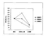
- Example 1 As shown in FIG. 5, the value of the elastic modulus of the diffusion preventing layer 12 decreases to about 260 [GPa], and the elastic modulus of the piezoelectric layer 13 decreases to about 115 [GPa]. For this reason, it can be seen that the difference between the elastic modulus of the diffusion preventing layer 12 and the elastic modulus of the substrate 7 and the piezoelectric layer 13 can be reduced. As a result, the elastic modulus gap between the films can be surely reduced. As a result, as shown in FIG. 6, the rate of film peeling can be suppressed to 16.7%, the rate of short circuit can be reduced to 0%, and the yield can be improved to 83.3%.
- Example 2 as shown in FIG. 5, the value of the elastic modulus of the diffusion preventing layer 12 is reduced to about 160 [GPa], and the elastic modulus of the piezoelectric layer 13 is reduced to about 70 [GPa].
- the elastic modulus of the diffusion preventing layer 12 can be reliably set to an intermediate value between the substrate 7 and the piezoelectric layer 13, and in particular, the elastic modulus value of the piezoelectric layer 13 can be greatly reduced.
- the elastic modulus gap between the films can be further reliably reduced.
- FIG. 6 it is possible to completely prevent the film peeling and the short circuit from occurring and to make the yield 100%.
- Example 3 In the step of forming the diffusion preventing layer 12, ZrO 2 powder (TZ-3YS manufactured by Tosoh): 160 g was used. Otherwise in the same manner as in Example 1 and Example 2, it was manufactured piezoelectric element 100 having a three-layer structure composed of SUS substrate / ZrO 2 / PZT.
- the film thickness of the diffusion preventing layer 12 is 5.0 ⁇ m or more, and in this example, three types of 5.0 ⁇ m, 9.9 ⁇ m, and 25.0 ⁇ m are used.
- the piezoelectric constant -d31 was 52 pm / V, 76 pm / V, and 34 pm / V.
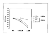
- FIG. 5 the measured values of the elastic modulus of the SUS substrate 7, the diffusion preventing layer 12, and the piezoelectric layer 13 are shown in FIG.
- Example 2 In the step of forming the diffusion preventing layer 12, the film thickness was 1.6 ⁇ m. Otherwise in the same manner as in Example 3 was prepared a piezoelectric element 100 having a three-layer structure composed of SUS substrate / ZrO 2 / PZT. The piezoelectric constant -d31 was 29 pm / V. Similarly to the above, the measured values of the elastic modulus of the SUS substrate 7, the diffusion preventing layer 12, and the piezoelectric layer 13 are shown in FIG.
- Example 3 the value of the elastic modulus of the diffusion preventing layer 12 is sufficiently lowered to about 180 to 230 [GPa], which is equal to or less than the standard bulk property of zirconia. Become.
- the elastic modulus of the diffusion preventing layer 12 can be reliably set to an intermediate value between the elastic modulus of the substrate 7 and the elastic modulus of the piezoelectric layer 13.
- the elastic modulus of the piezoelectric layer 13 is also greatly reduced to about 40 to 90 [GPa].
- the elastic modulus gap between the films can be surely reduced, and as in the first and second embodiments, the film peeling rate and the short-circuit rate can be suppressed, and the yield can be improved. .
Landscapes
- Chemical & Material Sciences (AREA)
- Engineering & Computer Science (AREA)
- Chemical Kinetics & Catalysis (AREA)
- Materials Engineering (AREA)
- Mechanical Engineering (AREA)
- Metallurgy (AREA)
- Organic Chemistry (AREA)
- Inorganic Chemistry (AREA)
- Manufacturing & Machinery (AREA)
- Ceramic Engineering (AREA)
- Physical Vapour Deposition (AREA)
- Particle Formation And Scattering Control In Inkjet Printers (AREA)
Abstract
【課題】膜剥離や短絡の発生を抑制し、かつ圧電特性を向上する。 【解決手段】基板7の上に、単一の拡散防止層12と、圧電層13とが、この順序で積層された、基板7を含めた3層構造の圧電素子100であって、拡散防止層12及び圧電層13は、それぞれエアロゾルデポジション法によって成膜された膜であり、拡散防止層12の弾性率は、基板7の弾性率以下でかつ圧電層13の弾性率以上の関係を有する。拡散防止層12は、アルミナを添加したジルコニア、若しくは、チタン酸ジルコン酸鉛、若しくは、膜厚が5μm以上となるジルコニアにより構成する。
Description
本発明は、エアロゾルデポジション法によって成膜した薄膜を圧電膜として有する圧電素子に関する。
インクジェットプリンタ等に用いられる圧電アクチュエータにおける圧電膜を形成する方法として、近年、エアロゾルデポジション法が注目されている。エアロゾルデポジション法は、気体中にセラミックス微粒子を分散して構成されるエアロゾルをノズルから噴射し、高速で基板表面に吹き付けることによって、基板上で微粒子を粉砕し堆積させてセラミックス薄膜を形成する成膜方法である。この方法は、基板表面へのセラミックス微粒子の衝突で発生する局所的な衝撃エネルギーが開放することに起因したメカノケミカル反応の誘起によって起こる常温衝撃固化現象を利用しており、粒子衝突時の衝撃力を膜形成時の反応エネルギーとして作用させる成膜技術である。
アニール処理は、エアロゾルデポジション法により形成された薄膜を加熱して薄膜内部の結晶粒を成長させて、薄膜の圧電特性等を向上させることを目的とする。このアニール処理によりステンレス中のFeやCrが圧電層に拡散し、圧電特性が低下してしまうことが知られている。これを防止するために、ステンレス基板と圧電層の間に、絶縁性セラミックス材料や、金属材料、導電性酸化物等により構成される拡散防止層を設けることによって上述の拡散を防止することが特許文献1にて提案されている。
しかしながら、上記従来技術には以下の問題が存在する。すなわち、エアロゾルデポジション法によりセラミックス膜により構成される上記拡散防止層を設けた場合、圧電層と拡散防止層との間に存在する大きな弾性率のギャップと、アニール処理による弾性率の大幅な変動によって、圧電層と拡散防止層との間で膜間応力が急激に増大する。この結果、上記アニール処理を行った後に、圧電層と拡散防止層との間の膜界面で、膜剥離が発生しやすくなるおそれがある。
あるいは、たとえ膜剥離が発生しなくとも、製造した圧電素子にクラックやピンホールが形成されてしまうことで圧電層を挟む一対の電極が導通して短絡する場合があり、圧電素子の歩留りが向上しないという問題もあった。これらに加えて、圧電素子の圧電特性についてもさらに改善することが望まれていた。
本発明の目的は、膜剥離や短絡の発生を抑制し、かつ圧電特性を向上できる圧電素子を提供することにある。
上記目的を達成するために、第1発明の圧電素子は、基板と、単一の拡散防止層と、圧電層とが、この順序で積層された3層構造の圧電素子であって、前記拡散防止層及び前記圧電層は、それぞれエアロゾルデポジション法によって成膜された膜であり、前記拡散防止層の弾性率は、前記基板の弾性率以下でかつ前記圧電層の弾性率以上の関係を有することを特徴とする。
第2発明の圧電素子は、上記第1発明において、前記拡散防止層を、前記エアロゾルデポジション法による成膜厚さが厚いほど弾性率が小さくなる材料粒子を用いて構成したことを特徴とする。
第3発明の圧電素子は、上記第1又は第2発明において、前記拡散防止層を、アルミナを添加したジルコニアにより構成したことを特徴とする。
第4発明の圧電素子は、上記第1又は第2発明において、前記拡散防止層を、チタン酸ジルコン酸鉛により構成したことを特徴とする。
第5発明の圧電素子は、上記第1又は第2発明において、前記拡散防止層を、膜厚が5μm以上となるジルコニアにより構成したことを特徴とする。
本発明によれば、基板の弾性率≧拡散防止層の弾性率≧圧電膜の弾性率となるような構成とすることにより、積層型圧電素子における各膜間の弾性率のギャップを少なくすることができる。したがって、膜剥離や短絡の発生を抑制し、かつ圧電特性を向上することができる。
(1)成膜の概略
(1-A)成膜装置の構成
図1に示す成膜装置は、キャリアガスに材料粒子を分散させてエアロゾルを発生させるためのエアロゾル生成器1と、内部で成膜を実施するためのチャンバ2とを備えている。
(1-A)成膜装置の構成
図1に示す成膜装置は、キャリアガスに材料粒子を分散させてエアロゾルを発生させるためのエアロゾル生成器1と、内部で成膜を実施するためのチャンバ2とを備えている。
エアロゾル生成器1には、所定量の材料粒子(例えば、粒径0.5μm~5.0μm程度のもの)が収納されており、キャリアガスが導入される。エアロゾル生成器1は、キャリアガス導入の際に巻き上げガスを発生させる。さらにエアロゾル生成器1は、材料粒子に対し下部から超音波加振装置若しくはキャリアガスの一部を用いた流動攪拌等による振動を加える。これにより、キャリアガスに材料粒子が分散されて、エアロゾルが発生する。キャリアガスとしては、例えば、ヘリウム、アルゴン等の不活性ガスや、窒素、空気、酸素等を使用することができる。
エアロゾル生成器1の上部にはエアロゾル供給管3の一端が挿入されている。エアロゾル供給管3の他端はチャンバ2の内部に配置され、噴射ノズル4が接続されている。
チャンバ2には、メカニカルブースターポンプとロータリーポンプ等が接続されており、これらのポンプはチャンバ2の内部を減圧する。この結果、チャンバ2の内圧がエアロゾル生成器1の内圧と比較して低圧になる。チャンバ2とエアロゾル生成器1との差圧によって、エアロゾル生成器1内で発生したエアロゾルがエアロゾル供給管3に吸い込まれ、噴射ノズル4に供給される。
噴射ノズル4の内部の空洞は、内部を進行するに従い横断面積が減少していくような形状を有している。この結果、噴射ノズル4の導入開口から噴射ノズル4の内部に進入したエアロゾルは、加速されたうえで、噴射ノズル4の射出開口から、エアロゾル流5として高速で基板7に吹き付けられる。基板7の表面に衝突した材料粒子は破砕し、堆積することによって、薄膜が形成される。
チャンバ2の内部には、噴射ノズル4の射出開口の上方に、基板7を下面に取り付けるための基板ホルダ6が配置されている。基板ホルダ6は矩形板状のものである。基板ホルダ6は駆動装置8によって水平姿勢でチャンバ2の天井からつり下げられている。駆動装置8は、基板ホルダ6を図1中の左右方向に駆動させる。この左右方向の駆動によって、基板7に対する走査成膜が行われる。この走査成膜によって、基板7の所定の広範な範囲に薄膜が形成される。
成膜対象物である基板7としては、ステンレス製の基板が挙げられるが、これに限定されず、例えば、他の金属、シリコン、半導体、樹脂等により構成される基板でもよい。
(1-B)圧電素子の層構造
図2に示す圧電素子100は、圧電アクチュエータとして用いられる形態の例である。圧電素子100は、基板7の上に複数層ではない単一の拡散防止層12が積層されている。拡散防止層12の上には下部電極15が形成されている。下部電極15の上には、圧電アクチュエータの変形に貢献する、圧電材料により構成される圧電層13が積層されている。そして、圧電層13の上には上部電極16が積層されている。このように、圧電素子100は、基板7、拡散防止層12および圧電層13の3層が積層された3層構造であり、拡散防止層12と圧電層13の間には下部電極15が形成されるとともに圧電層13の上には上部電極16が形成されている。拡散防止層12及び圧電層13は、それぞれ上述したエアロゾルデポジション法によって基板7上に成膜されている。
図2に示す圧電素子100は、圧電アクチュエータとして用いられる形態の例である。圧電素子100は、基板7の上に複数層ではない単一の拡散防止層12が積層されている。拡散防止層12の上には下部電極15が形成されている。下部電極15の上には、圧電アクチュエータの変形に貢献する、圧電材料により構成される圧電層13が積層されている。そして、圧電層13の上には上部電極16が積層されている。このように、圧電素子100は、基板7、拡散防止層12および圧電層13の3層が積層された3層構造であり、拡散防止層12と圧電層13の間には下部電極15が形成されるとともに圧電層13の上には上部電極16が形成されている。拡散防止層12及び圧電層13は、それぞれ上述したエアロゾルデポジション法によって基板7上に成膜されている。
下部電極15は、拡散防止層12と圧電層13との界面にある拡散防止層12の表面に全面にわたって設けられる。下部電極15は、アースされて常時グランド電位となるグランド電極として使用される。
上部電極16は、圧電層13の上表面に、複数の独立した領域によって電極パターンとして構成されている。上部電極16は、個々の領域それぞれにリード部が接続され、リード部を介して駆動回路ICに接続される。駆動回路ICに接続されることによって上部電極16は、駆動回路ICによって、グランド電位、若しくは、グランド電位とは異なる電位が、選択的に付与される駆動電極として使用される。下部電極15及び上部電極16は、例えばAu、Pt等の金属から構成される。
ここで、本実施形態の圧電素子100の特徴は、基板7の弾性率の値が拡散防止層12の弾性率の値以上となるように構成したことにある。また、拡散防止層12の弾性率の値が圧電層13の弾性率の値以上となるように構成する。この構成とすることによって、各層間の弾性率ギャップを小さくすることができる。
なお、各膜の弾性率は、ナノインデンテーション法によって測定することができる。具体的には、エリオニクス社製の超微小押込み硬さ試験機:ENT-1100aを用いて、押込み荷重を5mNとして測定した値である。また、ここでいう弾性率は、各層を形成した後アニール処理を行う以前に測定された値である。また、圧電特性は、電圧をかけたときの電極面に厚み方向の変形のし易さを示す圧電定数-d31の値を算出しこの値の大きさで評価した。この圧電定数-d31は、圧電アクチュエータの変位測定すること等の作業によって算出することができる。
(1-C)成膜手順
上記構成の本実施形態の圧電素子100の具体的な製法を以下に説明する。
上記構成の本実施形態の圧電素子100の具体的な製法を以下に説明する。
まず、基板7の表面に、上述したエアロゾルデポジション法により拡散防止層12を形成する。本実施形態では、拡散防止層12を成膜するときに材料粒子を構成する材料として、エアロゾルデポジション法による成膜厚さが厚いほど弾性率が小さくなる材料粒子を用いる。材料粒子の詳細な材料構成については後述する。この構成とすることにより、前述したような、基板7の弾性率以下でかつ圧電層13の弾性率以上となるような拡散防止層12の弾性率の設定を、エアロゾルデポジション法での成膜時における厚さ調整によって容易に行えるようにしている。
上記拡散防止層12の成膜後、表面の粉体を除去し、拡散防止層12の表面に、蒸着法やスパッタ法、あるいは金属粒子を含むペーストの塗布及び乾燥等によって、下部電極15を成膜する。続いて、拡散防止層12の応力を開放するために、比較的低温(およそ500℃程度)での加熱による応力開放アニール処理を行う。応力開放アニール処理は、エアロゾルデポジション法により形成された薄膜を加熱して、膜内に混入した成膜ガス及び水分等を除去するとともに、薄膜の残留応力を開放させる目的で行われる処理である。
上記応力開放アニール処理の後、下部電極15の表面に、再びエアロゾルデポジション法により圧電層13を形成する。この圧電層13を成膜するときの材料粒子としては、チタン酸バリウム、チタン酸鉛、マグネシウムニオブ酸鉛、ニッケルニオブ酸鉛、亜鉛ニオブ酸鉛等の圧電材料を使用することができる。
上記圧電層13の成膜後、表面の粉体を除去し、さらに、圧電層の結晶粒を成長させるため、比較的高温(およそ800~900℃程度)での加熱による粒成長アニール処理を行う。粒成長アニール処理とは、エアロゾルデポジション法により形成された圧電層13を加熱することにより、薄膜内部の結晶粒の成長や、格子欠陥の修正を達成し、薄膜の圧電特性等を向上させる目的で行われる処理である。上述のとおり、エアロゾルデポジション法により形成された圧電層13は、この粒成長アニール処理によって、その界面付近での弾性率が大きく変化する。しかしながら、上記した弾性率の関係を備えた本実施形態の層構成を採用することにより、膜剥離等の問題を回避することができる。
最後に、圧電層13の表面に、上部電極16を形成する。上部電極16を形成するには、マスキングをして蒸着法やスパッタ法を実施する。あるいは、蒸着法やスパッタ法により圧電層13の全面に金属層を形成した後、フォトリソグラフィ・エッチングを利用して所定のパターンに形成してもよい。また、圧電層13の表面に直接スクリーン印刷をすることによって上部電極16を形成してもよい。
以上により、本実施形態による圧電素子100が完成する。
(2)本発明の原理
上述したように、本実施形態においては、圧電素子100を、上部電極16及び下部電極15を除き、基板7、拡散防止層12、及び圧電層13の3層構造で構成する。さらにそれらの弾性率が、
基板7の弾性率 ≧ 拡散防止層12の弾性率 ≧ 圧電層13の弾性率
の関係となるように構成する。この構成とするのは、各膜間の弾性率ギャップを少なくするためである。
上述したように、本実施形態においては、圧電素子100を、上部電極16及び下部電極15を除き、基板7、拡散防止層12、及び圧電層13の3層構造で構成する。さらにそれらの弾性率が、
基板7の弾性率 ≧ 拡散防止層12の弾性率 ≧ 圧電層13の弾性率
の関係となるように構成する。この構成とするのは、各膜間の弾性率ギャップを少なくするためである。
すなわち、上述のようにエアロゾルデポジション法により拡散防止層12を設けた場合、圧電層13と拡散防止層12との間に存在する弾性率のギャップと、前述の粒成長アニール処理による弾性率の大幅な変動によって、圧電層13と拡散防止層12との間で膜間応力が急激に増大する。この結果、上記粒成長アニール処理を行った後に、圧電層13と拡散防止層12との間の膜界面で、膜剥離が発生しやすくなるおそれがある。
そこで、本実施形態では、基板7の弾性率 ≧ 拡散防止層12の弾性率 ≧ 圧電膜13の弾性率、となる構成とする。この構成とすることにより、圧電素子100における各膜間の弾性率のギャップを少なくすることができる。したがって、各層の間で発生する応力を低減して、圧電層13の界面剥離を発生しにくくすることができる。したがって、膜剥離の発生を抑制し、歩留まりを向上することができる。また、クラックやピンホールも形成されにくくなり、短絡の発生も抑制することができる。また、圧電層13の内部応力の低減によって、圧電素子100の圧電特性を向上させることができる。
(3)各実施形態
(3-A)第1実施形態及び第2実施形態
例えば基板としてステンレスを設け、チタン酸ジルコン酸鉛により構成される圧電層との間の拡散防止層として、アルミナを用いた従来構造の場合、基板の弾性率が260[GPa]程度、拡散防止層の弾性率が390[GPa]程度、圧電層の弾性率が120[GPa]程度となって、特に拡散防止層の弾性率が突出して大きいことにより、各膜間の弾性率のギャップが非常に大きくなる。
(3-A)第1実施形態及び第2実施形態
例えば基板としてステンレスを設け、チタン酸ジルコン酸鉛により構成される圧電層との間の拡散防止層として、アルミナを用いた従来構造の場合、基板の弾性率が260[GPa]程度、拡散防止層の弾性率が390[GPa]程度、圧電層の弾性率が120[GPa]程度となって、特に拡散防止層の弾性率が突出して大きいことにより、各膜間の弾性率のギャップが非常に大きくなる。
本発明の第1実施形態によると、拡散防止層12を、アルミナとジルコニアの中間特性を示すようにアルミナを添加したジルコニアにより構成する。
本願発明者等の検討によれば、拡散防止層12にアルミナ添加ジルコニアを用いると、基板7及び拡散防止層12の弾性率の値がそれぞれ260[GPa]程度、圧電層13の弾性率が115[GPa]程度となり、拡散防止層12の弾性率と、基板7及び圧電層13の弾性率との差を、小さくできることがわかった。
したがって、第1実施形態において、アルミナを添加したジルコニアを用いて拡散防止層12を構成することにより、積層型の圧電素子100における各膜間の弾性率のギャップを確実に少なくして膜剥離や短絡の発生を抑制することができる。
本発明の第2実施形態によると、拡散防止層12を、チタン酸ジルコン酸鉛により構成する。
本願発明者等の検討によれば、拡散防止層12にチタン酸ジルコン酸鉛を用いると、拡散防止層12の弾性率の値が160[GPa]程度、圧電層13の弾性率が70[GPa]程度となる。なお、基板7の弾性率の値は260[GPa]程度となる。この結果、拡散防止層12の弾性率を、確実に基板7の弾性率と圧電層13の弾性率との中間の値とすることができるとともに、特に圧電層13の弾性率の値を大きく低下させることがわかった。
したがって、第2実施形態において、拡散防止層12をチタン酸ジルコン酸鉛で構成することにより、積層型の圧電素子100における各膜間の弾性率のギャップを確実に少なくして膜剥離や短絡の発生を抑制できるとともに、圧電層13の弾性率自体が低下することによってさらに膜剥離や短絡の発生を防止することができる。
(3-B)第3実施形態
(a)ジルコニア膜による拡散防止効果の考察
上述したように、アニール処理により基板7のステンレス中のFeやCrが圧電層13へ拡散するのを防止するために拡散防止層12を設けることは既に知られており、ジルコニアを用いることも既に提唱されている。
(a)ジルコニア膜による拡散防止効果の考察
上述したように、アニール処理により基板7のステンレス中のFeやCrが圧電層13へ拡散するのを防止するために拡散防止層12を設けることは既に知られており、ジルコニアを用いることも既に提唱されている。
本願発明者等は、この拡散防止層12として用いられるジルコニアの拡散防止効果と膜厚との関係を検討し、図3に示すような結果を得た。
図3において、基板7のステンレス基材に含まれるFe,Crが、拡散防止層12内に拡散して入り込んでいるのがわかる。しかしながら、Fe及びCrも、基板7から拡散防止層12に侵入後、厚さ方向距離1μm程度でほぼ拡散が終了していることがわかる。言い換えれば、拡散防止層12としての機能を得る限りにおいては、ジルコニア層の厚さは高々1μm~2μm程度で十分であり、それ以上厚くしてもあまり意味がないことがわかった。なお、Ptは下部電極15の成分元素であり組成分析のベースライン及び圧電層13への拡散の有無を確認するために用いている。
(b)ジルコニア膜の膜厚と弾性率との関係
次に、本願発明者等は、ジルコニア膜厚の値と弾性率との関係を検討し、図4に示すような結果を得た。
次に、本願発明者等は、ジルコニア膜厚の値と弾性率との関係を検討し、図4に示すような結果を得た。
図4において、ジルコニアの膜厚が約1.6μmのときに弾性率の値が270[GPa]程度であり、以降、膜厚が大きくなるほど弾性率の値は減少し、膜厚が約5μmで弾性率の値は230[GPa]程度、膜厚が約10μmのときに弾性率の値が200[GPa]程度にまで下がり、ジルコニアの標準バルク特性と同等あるいはそれ以下となる。これ以降は、膜厚が大きくなってもあまり弾性率は低下せず、膜厚が約25μmのときに弾性率の値が190[GPa]程度となった。
以上により、拡散防止層12としての効果を得るにはジルコニア膜厚は1μm~2μm程度で十分であるものの、さらに厚さを増大させることで弾性率の値を所望の値に制御できる余地がある。そして、少なくとも5μm程度までジルコニア膜厚を増大させることで、弾性率を低減できる効果が得られることがわかった。
(c)層構成
本発明の第3実施形態によると、拡散防止層12を、膜厚が5μm以上となるジルコニアにより構成する。
本発明の第3実施形態によると、拡散防止層12を、膜厚が5μm以上となるジルコニアにより構成する。
したがって、第3実施形態において、拡散防止層12をジルコニアにより構成し、かつ膜厚を5μm以上とすることにより、積層型の圧電素子100における各膜間の弾性率のギャップを確実に少なくして膜剥離や短絡の発生を抑制できる。また、圧電層13の弾性率自体が低下することによってさらに膜剥離や短絡の発生を防止することができる。
以下に実施例を掲げて本発明をさらに詳細に説明するが、本発明はこれら実施例に限定されるものではない。
(実施例1)
1.基板の準備
幅15mm、奥行き35mm、厚さ0.4mmである拡散接合SUS基板(ヘッド)及び評価用SUS基板(弾性率測定)を準備した。ナノインデンターを用いて、荷重:5mNにて評価用SUS基板の弾性率を測定した。弾性率の値は図5に示す。
1.基板の準備
幅15mm、奥行き35mm、厚さ0.4mmである拡散接合SUS基板(ヘッド)及び評価用SUS基板(弾性率測定)を準備した。ナノインデンターを用いて、荷重:5mNにて評価用SUS基板の弾性率を測定した。弾性率の値は図5に示す。
2.拡散防止層の形成
これらの基板に対して、上述した実施形態に基づくエアロゾルデポジション法に基づいた成膜装置にて、拡散防止層12としてZrO2(20%Al2O3添加)膜を形成した。
これらの基板に対して、上述した実施形態に基づくエアロゾルデポジション法に基づいた成膜装置にて、拡散防止層12としてZrO2(20%Al2O3添加)膜を形成した。
以下、この工程を具体的に説明する。エアロゾル生成器1にZrO2(20%Al203添加)粉末(東ソー製TZ-3YS20A):160gを投入した。基板ホルダ6にSUS基板7をセットし、成膜範囲以外をテープで貼付した。基板ホルダ6をチャンバ2内の駆動装置8のXYステージにセットし、往復スキャンを開始した。なお、ステージ移動は2列(2枚)成膜を同一バッチにて行えるような移動態様とした。すなわち、ノズル4の噴射方向に対して2つの基板7,7を対向して並列配置した。そして、まず、(a)ノズル4を一方の基板7に向かって近づけて対向させた。その後、(b)ノズル4を噴射方向とほぼ直角に他方の基板7側へと移動して他方の基板7に対向させた。その後、(c)他方の基板7から一旦遠ざかるように移動させた。その後、(d)ノズル4を再び他方の基板7に向かって近づけて対向させた。そして、(e)ノズル4を噴射方向とほぼ直角に上記一方の基板7側へと移動させて、上記一方の基板7に対向させた。その後、(f)上記一方の基板7から遠ざかるように移動させた。以降、(a)~(f)の動きを繰り返すように、駆動装置8のXYステージを移動させた。チャンバ2を真空引きして、到達真空圧:10~20Paとした。キャリアガスを3系統(流動、破砕、加速)から導入し、原料粉体を流動攪拌した。キャリアガスの総流量(3系統の合計)を所定の総流量に合わせ、流動状態を見ながら流動ガス流量を一定流量に定めた。その後、破砕ガスと加速ガスの比率を変更することでエアロゾルの濃度を所望の濃度に調整した。成膜範囲外で空噴射:5minを行った後、所定の成膜時間で各SUS基板上にエアロゾルを噴射した。所定の成膜時間が終了した後、成膜ガスを止め、成膜室を真空開放した。基板ホルダをXYステージから取り外し、拡散防止層12が表面に形成されたSUS基板7を得た。
拡散防止層12が形成されたSUS基板7は表面をエアブローし、付着した粉体を除去した。段差計を用いて、SUS基板7上の拡散防止層12の膜厚を測定したところ、0.91~2.91μmであった。次に、ナノインデンターを用いて、荷重:5mNにて、評価用SUS基板上の拡散防止層12の弾性率を測定した。弾性率の値は図5に示す。
2.下部電極の形成
スパッタ装置を用いて、拡散防止層12の表面に、下部電極15となるTi(0.05μm)/Pt(0.5μm)層を形成した。
スパッタ装置を用いて、拡散防止層12の表面に、下部電極15となるTi(0.05μm)/Pt(0.5μm)層を形成した。
3.応力開放アニール処理
得られた各積層体をマッフル炉に投入して、500℃でのアニール処理を30分行い、Pt残留応力を開放した。
得られた各積層体をマッフル炉に投入して、500℃でのアニール処理を30分行い、Pt残留応力を開放した。
4.圧電層の形成
応力開放アニール処理後の各積層体に対して、上記同様のエアロゾルデポジション法にて、圧電層13としてPZT膜を形成した。なおこのとき用いた圧電材料粒子としては、堺化学工業製PZT-LQの粉末を用いた。
応力開放アニール処理後の各積層体に対して、上記同様のエアロゾルデポジション法にて、圧電層13としてPZT膜を形成した。なおこのとき用いた圧電材料粒子としては、堺化学工業製PZT-LQの粉末を用いた。
各積層体の表面をエアブローし、付着した粉体を除去した。段差計を用いて、SUS基板7上の圧電層13の膜厚を測定したところ、4.56~5.51μmであった。さらに、ナノインデンターを用いて、荷重:5mNにて、評価用SUS基板上の圧電層13の弾性率を測定した。弾性率の値は図5に示す。
7.粒成長アニール処理
得られた各積層体をマッフル炉に投入して、850℃でのアニール処理を30分行い、SUS基板7上のPZT結晶粒を成長させた。
得られた各積層体をマッフル炉に投入して、850℃でのアニール処理を30分行い、SUS基板7上のPZT結晶粒を成長させた。
上記の粒成長アニール処理後のPZT膜の外観形状を観察し、全面剥離があった場合は、膜剥離ありと判定した。多数のサンプルについて膜剥離の有無を判定し、全サンプル数に対する膜剥離が発生したサンプル数の割合を、膜剥離の発生率とした。膜剥離発生率の値は図6に示す。
8.上部電極の形成
拡散接合SUS基板上の圧電層13の表面に、メタルマスクを介して上部電極16となるAu(0.2μm)を形成した。これによって、SUS基板側から、SUS基板、ZrO2(20%Al2O3添加)、PZTの各層により構成される3層構造(以下適宜、「SUS基板/ZrO2+20%Al2O3/PZT」のようにスラッシュを用いて簡略化して示す)の圧電素子100を製造した。
拡散接合SUS基板上の圧電層13の表面に、メタルマスクを介して上部電極16となるAu(0.2μm)を形成した。これによって、SUS基板側から、SUS基板、ZrO2(20%Al2O3添加)、PZTの各層により構成される3層構造(以下適宜、「SUS基板/ZrO2+20%Al2O3/PZT」のようにスラッシュを用いて簡略化して示す)の圧電素子100を製造した。
9.電気評価
導通テスタを用いて、下部電極15:Pt、及び、上部電極16:Au層間の様々な箇所でのショート確認を行い、ショートの場合は電気評価を不良、測定可能な場合は電気評価を良好と判断した。多数のサンプルについて電気評価を行い、全サンプル数に対する電気評価が不良であったサンプル数の割合を、電気評価の不良率とした。不良率の値は図6に示す。
導通テスタを用いて、下部電極15:Pt、及び、上部電極16:Au層間の様々な箇所でのショート確認を行い、ショートの場合は電気評価を不良、測定可能な場合は電気評価を良好と判断した。多数のサンプルについて電気評価を行い、全サンプル数に対する電気評価が不良であったサンプル数の割合を、電気評価の不良率とした。不良率の値は図6に示す。
10.分極処理
まず、電気評価で良好と判断された欠陥のない箇所の上部電極16と下部電極15に、それぞれ電圧印加のための端子を接続した。そして、熱処理炉にて250℃に加熱してから各端子の間に、15分間の6kV/cmの電圧印加という分極条件にて、膜厚に相当する直流電圧を印加した。その後50℃まで冷却してから直流電圧の印加を停止し、最後に端子を取り外した。
まず、電気評価で良好と判断された欠陥のない箇所の上部電極16と下部電極15に、それぞれ電圧印加のための端子を接続した。そして、熱処理炉にて250℃に加熱してから各端子の間に、15分間の6kV/cmの電圧印加という分極条件にて、膜厚に相当する直流電圧を印加した。その後50℃まで冷却してから直流電圧の印加を停止し、最後に端子を取り外した。
11.変位測定
再び、上部電極16及び下部電極15に電圧印加のための端子を接続し、端子間に交流電圧(入力波形:0~20Vの正弦波、周波数4kHz)を印加し、そのときのアクチュエータの振動板である拡散接合SUS基板の動的変位をレーザドップラー法にて測定した。
再び、上部電極16及び下部電極15に電圧印加のための端子を接続し、端子間に交流電圧(入力波形:0~20Vの正弦波、周波数4kHz)を印加し、そのときのアクチュエータの振動板である拡散接合SUS基板の動的変位をレーザドップラー法にて測定した。
12.圧電定数の算出
圧電アクチュエータの構造体の変位と圧電定数の関係を、予め構造解析シミュレーションによって周波数応答性から解析した。このシミュレーション結果と上記の変位測定結果とを比較して、圧電定数-d31を算出した。本実施例においては、圧電定数-d31は、35pm/Vであった。
圧電アクチュエータの構造体の変位と圧電定数の関係を、予め構造解析シミュレーションによって周波数応答性から解析した。このシミュレーション結果と上記の変位測定結果とを比較して、圧電定数-d31を算出した。本実施例においては、圧電定数-d31は、35pm/Vであった。
(実施例2)
拡散防止層12の形成工程においてZrO2(20%Al2O3添加)粉末:160gの代わりに、PZT粉末(堺化学工業製PZT-LQ):200gを使用し、それ以外は実施例1と同様にして、SUS基板/PZT/PZTで構成される3層構造の圧電素子100を製造した。なお、拡散防止層12の膜厚は1.86~1.95μm、圧電層13の膜厚は5.15~5.23μmであった。本実施例においては、圧電定数-d31は、90pm/Vであった。実施例1と同様、SUS基板7、拡散防止層12、圧電層13の弾性率の測定値を図5に示し、膜剥離発生率及び不良率の値を図6に示す。
拡散防止層12の形成工程においてZrO2(20%Al2O3添加)粉末:160gの代わりに、PZT粉末(堺化学工業製PZT-LQ):200gを使用し、それ以外は実施例1と同様にして、SUS基板/PZT/PZTで構成される3層構造の圧電素子100を製造した。なお、拡散防止層12の膜厚は1.86~1.95μm、圧電層13の膜厚は5.15~5.23μmであった。本実施例においては、圧電定数-d31は、90pm/Vであった。実施例1と同様、SUS基板7、拡散防止層12、圧電層13の弾性率の測定値を図5に示し、膜剥離発生率及び不良率の値を図6に示す。
(比較例1)
拡散防止層12の形成工程においてAl2O3粉末(昭和電工製AL-160SG-4):140gを使用した。それ以外は実施例1及び実施例2と同様にして、SUS基板/Al2O3/PZTで構成される3層構造の圧電素子を製造した。圧電定数-d31は、21pm/Vであった。上記と同様、SUS基板7、拡散防止層12、圧電層13の弾性率の測定値を図5に示し、膜剥離発生率及び不良率の値を図6に示す。
拡散防止層12の形成工程においてAl2O3粉末(昭和電工製AL-160SG-4):140gを使用した。それ以外は実施例1及び実施例2と同様にして、SUS基板/Al2O3/PZTで構成される3層構造の圧電素子を製造した。圧電定数-d31は、21pm/Vであった。上記と同様、SUS基板7、拡散防止層12、圧電層13の弾性率の測定値を図5に示し、膜剥離発生率及び不良率の値を図6に示す。
(実施例1及び実施例2の考察結果)
以上の結果、比較例1では、図5に示すように、基板の弾性率が260[GPa]程度、拡散防止層の弾性率が390[GPa]程度、圧電層の弾性率が120[GPa]程度となる。特に拡散防止層の弾性率が突出して大きいことにより、各膜間の弾性率のギャップが非常に大きくなる。これにより、前述したように、粒成長アニール処理を行った後に、圧電層と拡散防止層との間の膜界面で、膜剥離が発生しやすくなるので、図6に示すように、膜剥離の発生率が44.4%と高く、さらに膜剥離が発生しなかった残りの55.6%のうち、短絡の発生により22.3%が電気的評価としては不合格となっている。したがって、実際の歩留まり率は33.3%という低率にとどまっている。
以上の結果、比較例1では、図5に示すように、基板の弾性率が260[GPa]程度、拡散防止層の弾性率が390[GPa]程度、圧電層の弾性率が120[GPa]程度となる。特に拡散防止層の弾性率が突出して大きいことにより、各膜間の弾性率のギャップが非常に大きくなる。これにより、前述したように、粒成長アニール処理を行った後に、圧電層と拡散防止層との間の膜界面で、膜剥離が発生しやすくなるので、図6に示すように、膜剥離の発生率が44.4%と高く、さらに膜剥離が発生しなかった残りの55.6%のうち、短絡の発生により22.3%が電気的評価としては不合格となっている。したがって、実際の歩留まり率は33.3%という低率にとどまっている。
これに対して、実施例1では、図5に示すように、拡散防止層12の弾性率の値が260[GPa]程度、圧電層13の弾性率が115[GPa]程度に下がる。このため、拡散防止層12の弾性率と、基板7及び圧電層13の弾性率との差を、小さくできることがわかる。この結果、各膜間の弾性率のギャップを確実に少なくすることができる。これにより、図6に示すように、膜剥離の発生率を16.7%まで抑制し、かつ短絡の発生率は0%とし、歩留まりを83.3%まで向上することができる。
また、実施例2では、図5に示すように、拡散防止層12の弾性率の値が160[GPa]程度、圧電層13の弾性率が70[GPa]程度にまで下がる。このため、拡散防止層12の弾性率を確実に基板7と圧電層13との中間の値とすることができ、特に圧電層13の弾性率の値を大きく低下させることができる。この結果、各膜間の弾性率のギャップをさらに確実に少なくすることができる。これにより、図6に示すように、膜剥離及び短絡の発生を完全に防止し、歩留まりを100%とすることができる。
(実施例3)
拡散防止層12の形成工程においてZrO2粉末(東ソー製TZ-3YS):160gを使用した。それ以外は実施例1及び実施例2と同様にして、SUS基板/ZrO2/PZTで構成される3層構造の圧電素子100を製造した。なお、拡散防止層12の膜厚は5.0μm以上とし、この例では5.0μm、9.9μm、25.0μmの3種類とした。圧電定数-d31は、52pm/V、76pm/V、34pm/Vであった。上記図5と同様、SUS基板7、拡散防止層12、圧電層13の弾性率の測定値を図7に示す。
拡散防止層12の形成工程においてZrO2粉末(東ソー製TZ-3YS):160gを使用した。それ以外は実施例1及び実施例2と同様にして、SUS基板/ZrO2/PZTで構成される3層構造の圧電素子100を製造した。なお、拡散防止層12の膜厚は5.0μm以上とし、この例では5.0μm、9.9μm、25.0μmの3種類とした。圧電定数-d31は、52pm/V、76pm/V、34pm/Vであった。上記図5と同様、SUS基板7、拡散防止層12、圧電層13の弾性率の測定値を図7に示す。
(比較例2)
拡散防止層12の形成工程において膜厚を1.6μmとした。それ以外は実施例3と同様にして、SUS基板/ZrO2/PZTで構成される3層構造の圧電素子100を製造した。圧電定数-d31は、29pm/Vであった。上記と同様、SUS基板7、拡散防止層12、圧電層13の弾性率の測定値を図7に示す。
拡散防止層12の形成工程において膜厚を1.6μmとした。それ以外は実施例3と同様にして、SUS基板/ZrO2/PZTで構成される3層構造の圧電素子100を製造した。圧電定数-d31は、29pm/Vであった。上記と同様、SUS基板7、拡散防止層12、圧電層13の弾性率の測定値を図7に示す。
(実施例3の考察結果)
以上の結果、比較例2では、図7に示すように、基板の弾性率が260[GPa]程度、拡散防止層の弾性率が270[GPa]程度となるが、圧電層の弾性率が230[GPa]程度である。この結果、拡散防止層の弾性率を基板の弾性率と圧電層の弾性率の中間の値とすることはできない。
以上の結果、比較例2では、図7に示すように、基板の弾性率が260[GPa]程度、拡散防止層の弾性率が270[GPa]程度となるが、圧電層の弾性率が230[GPa]程度である。この結果、拡散防止層の弾性率を基板の弾性率と圧電層の弾性率の中間の値とすることはできない。
これに対し、上記実施例3では、図示のように、拡散防止層12の弾性率の値が180~230[GPa]程度にまで十分に低下し、ジルコニアの標準バルク特性と同等あるいはそれ以下となる。この結果、拡散防止層12の弾性率を確実に基板7の弾性率と圧電層13の弾性率との中間の値にすることができる。またこのとき、圧電層13の弾性率も40~90[GPa]程度にまで大きく低下する。この結果、各膜間の弾性率のギャップを確実に少なくすることができるので、上記実施例1や実施例2と同様、膜剥離の発生率や短絡の発生率を抑制し、歩留まりを向上できる。
その他、本発明は、その趣旨を逸脱しない範囲内において、種々の変更が加えられて実施されるものである。
7 基板
12 拡散防止層
13 圧電層
100 圧電素子
12 拡散防止層
13 圧電層
100 圧電素子
Claims (5)
- 基板(7)と、単一の拡散防止層(12)と、圧電層(13)とが、この順序で積層された基板(7)を含めた3層構造の圧電素子であって、
前記拡散防止層(12)及び前記圧電層(13)は、それぞれエアロゾルデポジション法によって成膜された膜であり、
前記拡散防止層(12)の弾性率は、前記基板(7)の弾性率以下でかつ前記圧電層(13)の弾性率以上の関係を有する
ことを特徴とする圧電素子(100)。 - 前記拡散防止層(12)を、
前記エアロゾルデポジション法による成膜厚さが厚いほど弾性率が小さくなる材料粒子を用いて構成した
ことを特徴とする請求項1記載の圧電素子(100)。 - 前記拡散防止層(12)を、
アルミナを添加したジルコニアにより構成した
ことを特徴とする請求項1又は請求項2記載の圧電素子(100)。 - 前記拡散防止層(12)を、
チタン酸ジルコン酸鉛により構成した
ことを特徴とする請求項1又は請求項2記載の圧電素子(100)。 - 前記拡散防止層(12)を、
膜厚が5μm以上となるジルコニアにより構成した
ことを特徴とする請求項1又は請求項2記載の圧電素子(100)。
Applications Claiming Priority (2)
| Application Number | Priority Date | Filing Date | Title |
|---|---|---|---|
| JP2009080943A JP2010232580A (ja) | 2009-03-30 | 2009-03-30 | 圧電素子 |
| JP2009-080943 | 2009-03-30 |
Publications (1)
| Publication Number | Publication Date |
|---|---|
| WO2010116802A1 true WO2010116802A1 (ja) | 2010-10-14 |
Family
ID=42936090
Family Applications (1)
| Application Number | Title | Priority Date | Filing Date |
|---|---|---|---|
| PCT/JP2010/052697 Ceased WO2010116802A1 (ja) | 2009-03-30 | 2010-02-23 | 圧電素子 |
Country Status (2)
| Country | Link |
|---|---|
| JP (1) | JP2010232580A (ja) |
| WO (1) | WO2010116802A1 (ja) |
Cited By (1)
| Publication number | Priority date | Publication date | Assignee | Title |
|---|---|---|---|---|
| JP4868475B1 (ja) * | 2011-06-20 | 2012-02-01 | ムネカタ株式会社 | 圧電・焦電性膜の形成方法及び形成装置 |
Families Citing this family (3)
| Publication number | Priority date | Publication date | Assignee | Title |
|---|---|---|---|---|
| EP3341980B1 (de) * | 2015-08-26 | 2022-07-20 | CeramTec GmbH | Schicht und verfahren zu ihrer herstellung |
| EP3418428B1 (en) | 2016-02-19 | 2023-05-17 | Nippon Steel Corporation | Ceramic laminate, ceramic insulating substrate, and method for manufacturing ceramic laminate |
| JPWO2018216227A1 (ja) * | 2017-05-26 | 2020-03-26 | アドバンストマテリアルテクノロジーズ株式会社 | 膜構造体及びその製造方法 |
Citations (6)
| Publication number | Priority date | Publication date | Assignee | Title |
|---|---|---|---|---|
| JP2005279953A (ja) * | 2004-03-26 | 2005-10-13 | Fuji Photo Film Co Ltd | セラミックス構造物及びセラミックス構造物の製造方法 |
| JP2006173249A (ja) * | 2004-12-14 | 2006-06-29 | Fuji Photo Film Co Ltd | 圧電アクチュエータ及びその製造方法並びに液体吐出ヘッド |
| JP2006229154A (ja) * | 2005-02-21 | 2006-08-31 | Brother Ind Ltd | 圧電アクチュエータ、インクジェットヘッド、およびそれらの製造方法 |
| JP2007042740A (ja) * | 2005-08-01 | 2007-02-15 | Hitachi Cable Ltd | 圧電薄膜素子 |
| JP2007173400A (ja) * | 2005-12-20 | 2007-07-05 | Fujifilm Corp | 圧電アクチュエータの製造方法、液体吐出ヘッドの製造方法及び圧電アクチュエータ、液体吐出ヘッド並びに画像形成装置 |
| JP2008027961A (ja) * | 2006-07-18 | 2008-02-07 | Ngk Insulators Ltd | 誘電体デバイス |
-
2009
- 2009-03-30 JP JP2009080943A patent/JP2010232580A/ja active Pending
-
2010
- 2010-02-23 WO PCT/JP2010/052697 patent/WO2010116802A1/ja not_active Ceased
Patent Citations (6)
| Publication number | Priority date | Publication date | Assignee | Title |
|---|---|---|---|---|
| JP2005279953A (ja) * | 2004-03-26 | 2005-10-13 | Fuji Photo Film Co Ltd | セラミックス構造物及びセラミックス構造物の製造方法 |
| JP2006173249A (ja) * | 2004-12-14 | 2006-06-29 | Fuji Photo Film Co Ltd | 圧電アクチュエータ及びその製造方法並びに液体吐出ヘッド |
| JP2006229154A (ja) * | 2005-02-21 | 2006-08-31 | Brother Ind Ltd | 圧電アクチュエータ、インクジェットヘッド、およびそれらの製造方法 |
| JP2007042740A (ja) * | 2005-08-01 | 2007-02-15 | Hitachi Cable Ltd | 圧電薄膜素子 |
| JP2007173400A (ja) * | 2005-12-20 | 2007-07-05 | Fujifilm Corp | 圧電アクチュエータの製造方法、液体吐出ヘッドの製造方法及び圧電アクチュエータ、液体吐出ヘッド並びに画像形成装置 |
| JP2008027961A (ja) * | 2006-07-18 | 2008-02-07 | Ngk Insulators Ltd | 誘電体デバイス |
Cited By (2)
| Publication number | Priority date | Publication date | Assignee | Title |
|---|---|---|---|---|
| JP4868475B1 (ja) * | 2011-06-20 | 2012-02-01 | ムネカタ株式会社 | 圧電・焦電性膜の形成方法及び形成装置 |
| US8465810B2 (en) | 2011-06-20 | 2013-06-18 | Munekata Co., Ltd. | Method and device for forming piezoelectric/pyroelectric film |
Also Published As
| Publication number | Publication date |
|---|---|
| JP2010232580A (ja) | 2010-10-14 |
Similar Documents
| Publication | Publication Date | Title |
|---|---|---|
| JP5188076B2 (ja) | 圧電素子及びその製造方法、電子デバイス、インクジェット装置 | |
| JP2001152360A (ja) | セラミックス誘電体膜の形成方法、セラミックス誘電体膜/基板の積層構造体、及び電気−機械変換素子 | |
| US11805700B2 (en) | Laminated substrate having piezoelectric film, element having piezoelectric film and method for manufacturing this laminated substrate | |
| CN103348501B (zh) | 压电体膜、喷墨头、使用喷墨头形成图像的方法、角速度传感器、使用角速度传感器测定角速度的方法、压电发电元件以及使用压电发电元件的发电方法 | |
| EP3540797A1 (en) | Piezoelectric laminate, method of manufacturing piezoelectric laminate, and piezoelectric element | |
| JP2014072511A (ja) | 積層体 | |
| JP2010232580A (ja) | 圧電素子 | |
| WO2010076864A1 (ja) | 圧電素子 | |
| EP2677558B1 (en) | Piezoelectric element | |
| US7506441B2 (en) | Method for manufacturing a piezoelectric film on a substrate | |
| JP4894137B2 (ja) | 圧電アクチュエータおよびインクジェットヘッドの製造方法 | |
| US7622854B2 (en) | Piezoelectric element and film formation method for crystalline ceramic | |
| EP4174024A1 (en) | Piezoelectric laminate, piezoelectric element, and method for manufacturing piezoelectric laminate | |
| JP2009209413A (ja) | エアロゾルデポジション法の最適実施条件の選定方法、及び成膜方法 | |
| US7771780B2 (en) | Method of producing composite material, method of producing piezoelectric actuator, method of producing ink-jet head, and piezoelectric actuator | |
| JP2006229154A (ja) | 圧電アクチュエータ、インクジェットヘッド、およびそれらの製造方法 | |
| JP2021012909A (ja) | 圧電積層体、圧電素子および圧電積層体の製造方法 | |
| JP4094521B2 (ja) | 構造物の製造方法 | |
| JP2006297915A (ja) | 圧電アクチュエータ、インクジェットヘッドおよびそれらの製造方法 | |
| CN1919607B (zh) | 膜和喷墨头的制造方法 | |
| JP5384843B2 (ja) | 圧電素子構造体の製造方法および圧電素子構造体 | |
| JP2006261656A (ja) | 圧電アクチュエータおよびその製造方法 | |
| US7955647B2 (en) | Method for manufacturing film or piezoelectric film | |
| JP2009164313A (ja) | 電極パターン形成方法及び圧電アクチュエータの製造方法 | |
| JP4769979B2 (ja) | 圧電膜の製造方法 |
Legal Events
| Date | Code | Title | Description |
|---|---|---|---|
| 121 | Ep: the epo has been informed by wipo that ep was designated in this application |
Ref document number: 10761504 Country of ref document: EP Kind code of ref document: A1 |
|
| NENP | Non-entry into the national phase |
Ref country code: DE |
|
| 122 | Ep: pct application non-entry in european phase |
Ref document number: 10761504 Country of ref document: EP Kind code of ref document: A1 |