WO2010109705A1 - プローブおよびプローブの製造方法 - Google Patents
プローブおよびプローブの製造方法 Download PDFInfo
- Publication number
- WO2010109705A1 WO2010109705A1 PCT/JP2009/067629 JP2009067629W WO2010109705A1 WO 2010109705 A1 WO2010109705 A1 WO 2010109705A1 JP 2009067629 W JP2009067629 W JP 2009067629W WO 2010109705 A1 WO2010109705 A1 WO 2010109705A1
- Authority
- WO
- WIPO (PCT)
- Prior art keywords
- probe
- plating
- resist layer
- type resist
- forming
- Prior art date
- Legal status (The legal status is an assumption and is not a legal conclusion. Google has not performed a legal analysis and makes no representation as to the accuracy of the status listed.)
- Ceased
Links
Images





Classifications
-
- G—PHYSICS
- G01—MEASURING; TESTING
- G01R—MEASURING ELECTRIC VARIABLES; MEASURING MAGNETIC VARIABLES
- G01R3/00—Apparatus or processes specially adapted for the manufacture or maintenance of measuring instruments, e.g. of probe tips
-
- G—PHYSICS
- G01—MEASURING; TESTING
- G01R—MEASURING ELECTRIC VARIABLES; MEASURING MAGNETIC VARIABLES
- G01R1/00—Details of instruments or arrangements of the types included in groups G01R5/00 - G01R13/00 and G01R31/00
- G01R1/02—General constructional details
- G01R1/06—Measuring leads; Measuring probes
- G01R1/067—Measuring probes
- G01R1/06711—Probe needles; Cantilever beams; "Bump" contacts; Replaceable probe pins
- G01R1/06733—Geometry aspects
- G01R1/06738—Geometry aspects related to tip portion
-
- G—PHYSICS
- G11—INFORMATION STORAGE
- G11C—STATIC STORES
- G11C29/00—Checking stores for correct operation ; Subsequent repair; Testing stores during standby or offline operation
- G11C29/56—External testing equipment for static stores, e.g. automatic test equipment [ATE]; Interfaces therefor
-
- G—PHYSICS
- G11—INFORMATION STORAGE
- G11C—STATIC STORES
- G11C29/00—Checking stores for correct operation ; Subsequent repair; Testing stores during standby or offline operation
- G11C29/56—External testing equipment for static stores, e.g. automatic test equipment [ATE]; Interfaces therefor
- G11C29/56016—Apparatus features
-
- G—PHYSICS
- G01—MEASURING; TESTING
- G01R—MEASURING ELECTRIC VARIABLES; MEASURING MAGNETIC VARIABLES
- G01R1/00—Details of instruments or arrangements of the types included in groups G01R5/00 - G01R13/00 and G01R31/00
- G01R1/02—General constructional details
- G01R1/06—Measuring leads; Measuring probes
- G01R1/067—Measuring probes
- G01R1/06711—Probe needles; Cantilever beams; "Bump" contacts; Replaceable probe pins
- G01R1/06716—Elastic
- G01R1/06727—Cantilever beams
-
- G—PHYSICS
- G01—MEASURING; TESTING
- G01R—MEASURING ELECTRIC VARIABLES; MEASURING MAGNETIC VARIABLES
- G01R1/00—Details of instruments or arrangements of the types included in groups G01R5/00 - G01R13/00 and G01R31/00
- G01R1/02—General constructional details
- G01R1/06—Measuring leads; Measuring probes
- G01R1/067—Measuring probes
- G01R1/06711—Probe needles; Cantilever beams; "Bump" contacts; Replaceable probe pins
- G01R1/06755—Material aspects
- G01R1/06761—Material aspects related to layers
-
- G—PHYSICS
- G11—INFORMATION STORAGE
- G11C—STATIC STORES
- G11C29/00—Checking stores for correct operation ; Subsequent repair; Testing stores during standby or offline operation
- G11C29/56—External testing equipment for static stores, e.g. automatic test equipment [ATE]; Interfaces therefor
- G11C2029/5602—Interface to device under test
Definitions
- the present invention relates to a probe and a method for manufacturing the probe, and more particularly to a probe and a method for manufacturing the probe that can be suitably used when conducting a continuity test in contact with a fine electrode such as a chip test or a memory test.
- a probe is used when conducting a continuity test in contact with a fine electrode such as a chip test or a memory test.
- a fine electrode such as a chip test or a memory test.
- this probe adopting one of the shapes, as shown in FIG. 9, a micro cantilever (width 10 ⁇ m to 100 ⁇ m, thickness 10 ⁇ m) from the tip of a large probe body (width 100 ⁇ m, thickness 45 ⁇ m) 102 is used.
- (About 15 ⁇ m or so) 103 is a probe 101 having an overhang shape.
- Examples of the conventional method for manufacturing the probe 101 include a separate member bonding method, a two-step plating method, and a cutting formation method.
- the separate member bonding method is a method in which the probe main body 102 and the minute cantilever 103 are separately formed and then bonded together with an adhesive (see paragraph 0019 and FIG. 9 of Patent Document 1).
- the two-step plating method is a method in which the first plating mold is patterned on the A-type resist layer as the first step plating, the minute cantilever 103 is formed on the plating, and then the second step plating is performed on the B-type resist layer.
- the probe main body 102 is formed by plating after the plating mold is patterned.
- the cutting formation method is a method of cutting out the minute cantilever 103 by plating the probe main body 102 and cutting the tip thereof by ion milling or the like.
- the current cutting accuracy is lower than the desired accuracy, so that a micro cantilever 103 having a desired size is obtained. There was a problem that could not.
- the two-step plating method causes the problem of interfacial peeling because the plating is performed in two steps. If the one-step plating method in which the probe main body 102 and the minute cantilever 103 are plated at a time is adopted, the interfacial peeling is caused. The problem could be solved, but this also had the following problems.
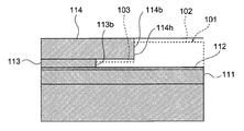
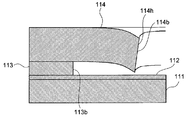
- the probe 101 is manufactured by the one-step plating method, as shown in FIG. 10, in order to form the probe 101 by plating, a plating mold 113b formed by each resist pattern for the A-type resist layer 113 and the B-type resist layer 114, 114b is required.
- the overhang portion 114h is inevitably formed in the plating molds 113b and 114b.
- the B-type resist layer 114 is formed using a dry film resist that has been hardened in advance.
- the overhang portion 114h is heated when the dry film resist is thermocompression bonded to the A-type resist layer 113. Therefore, it will be bent and deformed downward to close the cavity below the overhang portion 114h. In this case, the development rinse and the plating solution used for the resist pattern do not flow into the cavity below the overhang portion 114h, resulting in residual development residue and insufficient plating solution. Therefore, the micro cantilever 103 is formed in a desired shape and size. As a result, there is a problem that the micro cantilever 103 cannot exhibit desired performance.
- the present invention has been made in view of these points, and can improve the coupling force between the probe main body and the micro cantilever, and can form the micro cantilever overhanging from the probe main body in a desired shape and size. It is an object of the present invention to provide a probe that can be formed in a simple manner and a method for producing the probe.
- the present invention can improve the coupling force between the probe main body and the protruding portion (including the micro cantilever), and overhangs from the intermediate portion excluding one of the top, bottom, left and right near the tip of the probe main body. It is an object of the present invention to provide a probe that can form a hung protrusion in a desired shape and size, and a method for manufacturing the probe.
- the probe manufacturing method of the present invention is a base plate for manufacturing a probe adopting a shape in which a minute cantilever is overhanged from the tip of a probe body as a first aspect.
- Forming an underlayer using a liquid resist or dry film resist on the surface of the substrate, and a thickness comparable to the thickness of the microcantilever using the liquid resist or dry film resist on the surface of the underlayer Forming a part of the probe body and a part of the plating mold to be used for plating formation of the entire micro-cantilever with respect to the A-type resist layer, A seed film forming step of forming a seed film on the underlayer before or after the plating mold partial forming step A, and plating
- a hydrophilic treatment step A for performing hydrophilic treatment on the surface of the A-type resist layer and at least the surface of the A-type resist layer of the seed film, and the A-type resist layer subjected to the hydrophilic treatment
- a hydrophilic treatment step A for performing hydrophilic treatment on the
- the plating mold After forming on the surface and a part of the plating mold, if the remaining part of the plating mold for use in forming the remaining part of the probe body is not formed in the B-type resist layer in advance, the plating mold is applied to the B-type resist layer.
- a plating process for forming a probe in which a micro-cantilever is overhanged and a removing process for removing a B-type resist layer, a seed film unnecessary for the probe, an A-type resist layer, and an underlayer. It is said.
- the surface of the A-type resist layer is subjected to a hydrophilic treatment so that the A-type resist layer and the dry film resist are firmly fixed. It is possible to eliminate the thermocompression bonding of the dry film resist that causes the curved deformation of the portion.
- the development rinse and the plating solution can be made to flow easily in a gap (a gap below the overhang portion of the plating mold) where the minute cantilever is formed by plating in the plating mold. . Thereby, a micro cantilever can be formed in a desired shape and size.
- a probe manufacturing method comprising: a liquid resist on a surface of a substrate that serves as a base plate for manufacturing a probe having a shape in which a protruding portion is overhanged from an intermediate portion near the tip of a probe body.
- an underlayer forming step of forming an underlayer using a dry film resist, and a thickness similar to the thickness from the lower surface of the probe body to the lower surface of the protruding portion using a liquid resist or a dry film resist on the surface of the underlayer After forming a C-type resist layer having a thickness, a plating mold part forming step C for forming a part of a plating mold used for plating a part of the probe body on the C-type resist layer; After forming an A-type resist layer having a thickness similar to the thickness of the protrusion using a liquid resist or a dry film resist on the surface of the resist layer, A plating mold part forming step A for forming a part of the plating mold used for plating a part of the probe main body and the whole protruding part with respect to the mold resist layer, and a plating mold before the plating mold part forming process C A seed film forming step of forming a seed film on the underlayer either after the partial forming step A, and
- a plating mold part forming step B for forming the remaining part of the plating mold in the B type resist layer, and a plating mold part forming process when the remainder of the plating mold for use in forming the plating is not formed in the B type resist layer in advance.
- a plating process for forming a probe with overhanging protrusions by performing plating using the plating mold and seed film completed by the end of B, a B-type resist layer, a seed film unnecessary for the probe, A And a removing step of removing the C-type resist layer, the C-type resist layer, and the base layer.
- the surface of the A-type resist layer is subjected to a hydrophilic treatment, and the A-type resist layer and the dry film resist are firmly fixed. It is possible to eliminate the thermocompression bonding of the dry film resist that causes the curved deformation of the portion. Further, when the seed film is also subjected to a hydrophilic treatment, the development rinse and the plating solution can be made to easily flow into the gap where the protruding portion is plated in the plating mold (the gap below the overhang portion of the plating mold). . Thereby, a protrusion part can be formed in a desired shape and dimension. Furthermore, since this manufacturing method includes the plating mold part forming step C, it is possible to form a protruding portion at an intermediate portion near the tip of the probe body.
- the probe manufacturing method according to the third aspect of the present invention is the probe manufacturing method according to the first or second aspect, wherein the B-type resist layer is formed after the plating mold part forming step B and before the plating treatment step.
- a D-type resist layer is formed on the surface of the B-type resist layer and above the plating mold to close the upper opening of the plating mold formed by the steps up to the plating mold partial forming step B.
- a plating mold partial formation step D, and the thickness of the B-type resist layer in the plating mold partial formation step B is a thickness obtained by subtracting the thickness of the micro cantilever from the thickness of the probe body. Is formed equal to the thickness from the upper surface of the protrusion to the upper surface of the probe body, and the plating process in the plating process is performed after the plating mold part forming process D is completed, and in the removing process, the D-type resist layer is formed. It is also characterized by removal.
- the plating thickness is controlled not by the plating time but by the inner dimension of the plating mold. can do. Thereby, the dimensional accuracy of the probe formed by plating can be improved.
- the probe manufacturing method according to the fourth aspect of the present invention is characterized in that, in the probe manufacturing method according to one of the first to third aspects, the hydrophilic treatment is a plasma etching process.
- the adhesion between the A-type resist layer and the dry film resist is improved. be able to.
- the probe manufacturing method according to the fifth aspect of the present invention is the probe manufacturing method according to one of the first to third aspects, wherein the hydrophilic treatment is performed by applying a metal film having excellent hydrophilicity to an A-type resist layer. It is the metal film production
- the adhesion force between the A-type resist layer and the dry film resist is increased. Can be improved.
- the probe manufacturing method according to the sixth aspect of the present invention is the probe manufacturing method according to any one of the first to fifth aspects, wherein the seed film forming step is performed before the plating mold portion forming step A. It is characterized by.
- the surface of the underlayer becomes smooth and the adhesion area of the surface increases, so that the adhesion between the underlayer and the A-type resist layer is improved. Can do.
- the probe manufacturing method according to the seventh aspect of the present invention is the probe manufacturing method according to any one of the first to sixth aspects, wherein the seed film is a metal film having excellent conductivity and hydrophilicity. It is a feature.
- the development rinse and the plating solution easily flow into the gap of the plating mold that becomes the mold of the micro cantilever.
- the cantilever can be formed in a desired shape and size.
- the probe of the present invention includes, as a first aspect thereof, a probe main body and a micro cantilever overhanged from the tip of the probe main body.
- the probe main body and the micro cantilever are It is characterized by being integrally formed by a single plating process.
- the probe main body and the micro cantilever are integrally formed by one plating process, it is possible to prevent an interface from being generated between the probe main body and the micro cantilever. it can.
- the probe according to the second aspect of the present invention is characterized in that, in the probe according to the first aspect, the micro cantilever is overhanging from one end of the tip of the probe body.
- the probe according to the third aspect of the present invention includes a probe main body and a protruding portion overhanging from an intermediate portion near the tip of the probe main body.
- the probe main body and the protruding portion are formed by a single plating process. It is characterized by being integrally formed.
- the probe of the third aspect of the present invention is the probe of the first aspect, and the microcantilever is located near the tip of the probe body. It can be said that it is characterized by overhanging from the middle part.
- the protruding portion is a portion that protrudes from the probe body with one end fixed to the probe body and the other end as a free end, and includes both a minute cantilever and a simple protrusion that does not have a cantilever function. It is a waste.
- the probe main body and the protruding portion are integrally formed by one plating process, it is possible to prevent the occurrence of an interface between the probe main body and the protruding portion. it can.
- the binding force between the probe main body and the micro cantilever can be improved.
- the protruding portion is overhanging from the intermediate portion in the vicinity of the tip of the probe body, when the probe body is bent with the probe body as a cantilever and the protruding portion as a contact point, It is possible to prevent the probe body from being bent while being twisted.
- the plating mold is formed into a desired shape by preventing the bending deformation of the overhang portion of the plating mold, and the flow of the development rinse and the plating solution is improved.
- various problems such as interfacial peeling and dimensional accuracy can be solved, and the effect of being able to form a minute cantilever or protrusion overhanging from the probe body in a desired shape and size.
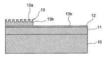
- the longitudinal cross-sectional view which shows the manufacturing method of the probe of 1st Embodiment in this invention in order from A to G Longitudinal sectional view showing an example (plasma etching treatment) of hydrophilic treatment of the first embodiment
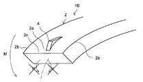
- the perspective view which shows an example of the probe of 2nd Embodiment in A or B in a figure
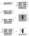
- the longitudinal cross-sectional view which shows the manufacturing method of the probe of 2nd Embodiment in order from A to G Perspective surface showing the bent state of the cantilever with the protruding part formed at the end of the tip of the cantilever body
- Perspective surface showing the bent state of the cantilever with the protruding part formed at the end of the tip of the cantilever body
- the perspective view which shows
- the probe 1A of the first embodiment includes a probe main body 2 and a minute cantilever 3 as shown in FIG.
- the dimensions and shapes of the probe main body 2 and the minute cantilever 3 are the same as conventional ones.
- the probe main body 2 and the minute cantilever 3 are integrally formed by a single plating process.
- the plating material for example, a metal having excellent spring properties such as Ni—P is selected.
- a metal having excellent conductivity may be formed on the surface of the probe 1A.
- the manufacturing method of the probe 1A of the first embodiment includes an underlayer forming process, a seed film forming process, a plating mold part forming process A, a hydrophilic treatment process A, and a plating mold part forming process B. And a plating treatment step and a removal step.
- a base layer 11 having a uniform thickness is formed on the surface of the substrate 10 serving as a base plate. Since the underlayer 11 is removed in the removing step, it is formed using a liquid resist or a dry film resist.
- a seed film 12 having a uniform thickness is formed on the surface of the base layer 11 using a film forming apparatus such as sputtering.
- This seed film forming step may be performed either before or after the plating mold partial forming step A.
- the seed film forming process of the first embodiment is performed before the plating mold part forming process A as shown in FIG. 1B.
- a metal film having excellent conductivity and hydrophilicity such as Cu is preferably selected.
- an A-type resist layer 13 is formed on the upper surface of the base layer 11 with a uniform thickness (see FIG. 1C).
- the A-type resist layer 13 is formed using a liquid resist or a dry film resist.
- the thickness of the A-type resist layer 13 is set to the same thickness as that of the minute cantilever 3, that is, an extremely thin thickness of about 10 ⁇ m to 15 ⁇ m. It is preferable to form the resist layer 13.
- a resist pattern to be a part 13b of the plating mold is formed on the A type resist layer 13.
- a part 13b of the plating mold is used to form a part of the probe main body 2 and the entire micro cantilever 3.
- the part of the probe body 2 is a part from the lower surface of the probe body 2 to a height similar to the thickness of the micro cantilever 3 from the viewpoint of the plating process.
- the seed film forming step is performed after the plating mold partial forming step A, the seed film 12 is not formed between the base layer 11 and the A type resist layer 13, and the A type resist layer 13 is formed.
- the seed film 12 is formed only on the surface of the base layer 11 exposed from the part 13b of the plating mold.
- the surface 13a of the A-type resist layer 13 is subjected to a hydrophilic treatment.
- the hydrophilic treatment process A may be performed after the plating mold part forming process A. Therefore, in other embodiments, the respective steps may be performed in the order of the plating mold part forming step A, the hydrophilic treatment step A, and the seed film forming step. Further, as in the first embodiment, when the hydrophilic treatment process A is performed after the plating mold part forming process A and the seed film forming process, not only the surface 13a of the A type resist layer 13 but also the seed film 12 is used. Also, hydrophilic treatment may be performed.
- hydrophilic treatment a plasma etching process for roughening the surface 13a of the A-type resist layer 13 may be used, or as shown in FIG. 3, a metal film 15 having excellent hydrophilicity may be used as the A-type resist layer.
- 13 may be a metal film generating process for forming a film on the surface 13a.
- the plasma etching process is selected as the hydrophilic process of the first embodiment.
- O 2 gas is selected because of good etching selectivity with the metal film 15.
- a dry film resist is applied to the A-type resist layer 13 that has been subjected to a hydrophilic treatment, and the B-type resist layer is placed above the surface 13a of the A-type resist layer 13 and a part 13b of the plating mold. 14 (see FIG. 1E).
- the dry film resist is stuck only by the adhesive force of the adhesive layer, and the thermocompression bonding is not performed.
- the thickness of the dry film resist serving as the B-type resist layer 14 is set to be equal to or greater than the thickness of the probe body 2 excluding the thickness of the minute cantilever 3.
- a resist pattern to be the remaining part 14b of the plating mold is formed on the B-type resist layer 14.
- the remaining part 14b of the plating mold is used for plating formation of the remaining part of the probe body 2.
- the remaining part of the probe body 2 is a part obtained by excluding a part of the probe body 2 described above from the entire probe body 2 from the viewpoint of the plating process.
- the plating mold remainder 14b is previously formed to the thickness of the dry film resist to be the B-type resist layer 14, it is not necessary to form the plating mold remainder 14b after the dry film resist is applied.
- the plating solution is filled into the finished plating molds 13b and 14b composed of the plating mold part 13b and the remaining part 14b, and then the seed film 12 is energized to perform plating. Perform processing.
- the probe 1A is formed by plating and growing from the seed film 12 and overhanging the minute cantilever 3.
- the plating material for example, a metal having excellent spring properties such as Ni—P is selected.
- unnecessary parts for the probe 1A such as the B-type resist layer 14, the seed film 12 unnecessary for the probe 1A, the A-type resist layer 13 and the base layer 11 are removed.
- the B-type resist layer 14, the unnecessary seed film 12, the A-type resist layer 13, and the base layer 11 may be removed one by one in order, or the seed film 12 may be removed after the resist is collectively removed.
- a metal having excellent conductivity may be formed on the surface of the probe 1A after the removing step.
- the thickness of the B-type resist layer 14 is set to be equal to the thickness obtained by excluding the thickness of the minute cantilever 3 from the thickness of the probe body 2. Further, the hydrophilic treatment process B and the plating mold part forming process D are performed after the plating mold part forming process B and before the plating process.
- the surface 14 a of the B-type resist layer 14 is subjected to a hydrophilic treatment.
- the content of the hydrophilic treatment is the same as the hydrophilic treatment performed in the hydrophilic treatment step A.
- a dry film resist is applied to the B-type resist layer 14 that has been subjected to the hydrophilic treatment without thermocompression bonding.
- This affixing method is the same as the affixing method of the B-type resist layer 14 in the plating mold part forming step B.
- the D-type resist layer 17 is formed above the surface 14a of the B-type resist layer 14 and the plating dies 13b and 14b. Since the plating molds 13b and 14b formed through the processes up to the plating mold partial forming process B have an upper opening, the D-type resist layer 17 serves as a lid for closing the plating molds 13b and 14b.
- the plating molds 13b and 14b are sealed by the formation of the D-type resist layer 17, it is preferable to provide an inlet for injecting a plating solution into a part of the plating molds 13b and 14b.
- plating mold part forming step D plating is performed in the plating process, and the D-type resist layer 17 is also removed in the removal process.
- the probe main body 2 and the minute cantilever 3 are integrally formed by a single plating process. Therefore, unlike the prior art, an interface does not occur between the probe main body 2 and the micro cantilever 3, so that it is possible to prevent the probe 1A from being destroyed by interfacial peeling from between them.
- the coupling force between the probe main body 2 and the micro cantilever 3 is improved. Can do.
- the surface 13a of the A-type resist layer 13 has been subjected to hydrophilic treatment, so that the dry film resist is not subjected to thermocompression bonding.
- the A-type resist layer 13 and the dry film resist can be firmly fixed only by the adhesive force.
- the plating type overhang portion 14h can be prevented from being bent and deformed by heat. Therefore, a gap in which the minute cantilever 3 is formed in the plating die 13b, that is, below the plating type overhang portion 14h. It is possible to prevent the cavity from being blocked.
- the development rinse and the plating solution are applied to the gap where the minute cantilever 3 is plated in the plating molds 13b and 14b, that is, the gap below the overhang portion 14h of the plating mold. It can be made easy to flow. Thereby, the micro cantilever 3 can be formed in a desired shape and size.
- the hydrophilic treatment is preferably a plasma etching treatment as shown in FIG.
- the surface 13a of the A-type resist layer 13 becomes rough, and an anchor effect is generated on the surface, so that the adhesion between the A-type resist layer 13 and the dry film resist can be improved.
- the hydrophilic treatment described above may be a metal film generating treatment in which a metal film 15 having excellent hydrophilicity is formed on the surface 13a of the A-type resist layer 13 as shown in FIG.
- a metal film 15 having excellent hydrophilicity is formed on the surface 13a of the A-type resist layer 13 as shown in FIG.
- the seed film forming step is preferably performed before the plating mold portion forming step A as shown in FIG. 1B.
- the seed film 12 is formed between the base layer 11 and the A-type resist layer 13.
- the surface of the foundation layer 11 becomes smooth and the adhesion area of the surface increases, so that the adhesion force between the foundation layer 11 and the A-type resist layer 13 is increased. Can be improved.
- the seed film 12 is preferably a metal film having excellent conductivity and hydrophilicity.
- the development rinse and the plating solution easily flow in the gap where the minute cantilever 3 is formed in the plating mold 13b, so that the minute cantilever 3 has a desired shape and size. Can be formed.
- the optional hydrophilic treatment step B and plating mold portion forming step D are performed after the plating mold portion forming step B and before the plating treatment step.
- the D-type resist layer 17 functions as a lid for the plating dies 13b and 14b.
- the element that controls the plating thickness is the plating time, and therefore it is difficult to precisely control the plating thickness.
- FIG. 1 shows that the element that controls the plating thickness is the plating time, and therefore it is difficult to precisely control the plating thickness.
- the D-type resist layer 17 serves as a lid for the plating molds 13b and 14b, if the plating time for reaching the D-type resist layer 17 has passed, Even if the plating time is increased as described above, the D-type resist layer 17 controls the thickness of the plating. That is, according to the probe manufacturing method of the first embodiment, the plating thickness can be controlled not by the plating time but by the inner dimensions of the plating molds 13b and 14b, so that the dimensional accuracy of the probe formed by plating is improved. Can be made.
- the plating molds 13b and 14b are formed in a desired shape by preventing the bending deformation of the overhang portion 14h of the plating molds 13b and 14b. Since the development rinse and the fluidity of the plating solution are improved, various problems such as interfacial peeling and dimensional accuracy can be solved, and the micro-cantilever 3 overhanging from the probe body 2 can be formed in a desired shape and size. There is an operational effect.
- the probe 1B of the second embodiment includes a probe main body 2 and a protruding portion 4.
- the protruding portion 4 is a portion that is fixed to the probe body 2 at one end and protrudes from the probe body 2 with the other end as a free end. Therefore, the protrusion part 4 of 2nd Embodiment contains not only the micro cantilever shown in FIG. 5A but the mere protrusion part which does not have the cantilever function shown in FIG. 5B.
- the probe main body 2 and the protrusion 4 in the second embodiment are integrally formed by a single plating process.
- the plating material for example, a metal having excellent spring properties such as Ni—P is selected.
- a metal having excellent conductivity may be formed on the surface of the probe 1B.
- the difference from the first embodiment is the overhang position of the protrusion 4 in the vicinity of the tip 2c of the probe body 2.
- the micro cantilever 3 of the first embodiment has a lower end at the distal end 2c of the probe main body 2 (by changing the direction of the probe main body 2, this lower end is That is, it is overhanging from the right end, i.e., any one end 2b at the tip 2c of the probe body 2).
- the protruding portion 4 of the second embodiment overhangs from the intermediate portion 2a in the vicinity of the tip 2c of the probe body 2 as shown in FIGS. 5A and 5B.
- the intermediate portion 2a in the vicinity of the distal end 2c of the probe body 2 is, for example, as shown in FIG. 5A, a portion excluding each end portion 2b on the distal end surface of the probe body 2, or as shown in FIG. A portion excluding both ends 2b in the width direction with respect to the bending direction in the tip 2c of the probe body 2 or a region adjacent to the tip 2c.
- the manufacturing method of the probe 1B of the second embodiment includes a base layer 11 forming step, a plating mold part forming process C, a seed film 12 forming process, a plating mold part forming process A, and hydrophilicity. It includes a processing step A, a plating mold part forming step B, a hydrophilic processing step B, a plating mold part forming step D, a plating processing step and a removal step.
- a step greatly different from the first embodiment is a plating mold part forming step C.
- the hydrophilic treatment process B and the plating mold part forming process D are optional processes.
- the protrusion 4 is formed to overhang, for example, to the left. Therefore, for example, in the case of the probe 1B shown in FIG. 5B, the probe 1B is formed in a state in which the direction of the probe 1B is changed so as to overhang the left side of FIG. 6G.
- the base layer 11 is formed on the surface of the substrate 10 using a liquid resist or a dry film resist, as shown in FIG. 6A.
- the C-type resist layer 18 is formed with a uniform thickness on the surface of the base layer 11 using a liquid resist or a dry film resist.
- the thickness of the C-type resist layer 18 is set to be approximately the same as the thickness from the lower surface of the probe 1B main body to the lower surface of the protruding portion 4 from the viewpoint of the plating process.
- a resist pattern that forms a part of a plating mold used for plating a part of the probe main body 2 on the C-type resist layer 18 is formed.
- a part 18b of the plating mold is used for forming a plating in the lower part of the probe body 2.
- the seed film 12 forming step is performed after the plating mold partial forming step C, the seed film 12 is not formed between the base layer 11 and the C-type resist layer 18, and the plating type of the C-type resist layer 18 is formed.
- the seed film 12 is formed only on the surface of the base layer 11 exposed from the part 18b of the substrate.
- the seed film 12 is formed on the underlayer 11 either before the plating mold part forming process C or after the plating mold part forming process A.
- the seed film 12 forming step is preferably performed before the plating mold portion forming step C as shown in FIG. 6A.
- the seed film 12 is preferably a metal film having excellent conductivity and hydrophilicity, as in the first embodiment.
- the A-type resist layer 13 is formed on the surface of the C-type resist layer 18. Similar to the first embodiment, the A-type resist layer 13 is formed using a liquid resist or a dry film resist, and the thickness thereof is the same as the thickness of the protrusion 4. After the formation of the A-type resist layer 13, a resist pattern is formed on the A-type resist layer 13. The A-type resist layer 13 on which the resist pattern is formed becomes a part 13b of a plating mold used for plating a part of the probe main body 2 and the whole protrusion 4.
- the part of the probe main body 2 in the plating mold part forming step A is a part located on the side of the protruding part 4 in the probe main body 2 from the viewpoint of the plating process, and a part having the same thickness as the thickness of the protruding part 4 It is.
- the surface 13a of the A-type resist layer 13 and at least the surface 13a of the A-type resist layer 13 of the seed film 12 Apply hydrophilic treatment.
- the content of the hydrophilic treatment is the same as the hydrophilic treatment in the first embodiment.
- a B-type resist layer 14 is formed on the surface and above the plating molds 18b and 13b.
- the thickness of the B-type resist layer 14 is equal to the thickness from the upper surface of the protrusion 4 to the upper surface of the probe body 2.
- the plating mold part forming step D which is an optional step, is not performed, the thickness of the B-type resist layer 14 is not less than the thickness from the upper surface of the protrusion 4 to the upper surface of the probe body 2. Good.
- a resist pattern is formed on the B-type resist layer 14 to form the remaining part 14b of the plating mold.
- the plating mold remainder 14b is formed in advance on the B-type resist layer 14
- a resist pattern is formed on the surface of the A-type resist layer 13 and the B-type resist layer 14 affixed above the plating mold. There is no need.
- the surface 14a of the B-type resist layer 14 is subjected to a hydrophilic treatment.
- This hydrophilic treatment is the same as in the first embodiment.
- the hydrophilic treatment process B is an optional process, and is performed after the plating mold part forming process B and before the plating process.
- the D-type resist layer 17 is formed by applying a dry film resist to the B-type resist layer 14 subjected to the hydrophilic treatment without thermocompression bonding. It is formed above the surface of the B-type resist layer 14 and the plating mold.
- the D-type resist layer 17 serves as a lid that closes the upper openings of the plating dies 18b, 13b, and 14b formed by the steps up to the plating die partial formation step B.
- this plating mold part forming step D is an optional step, as in the first embodiment, and is performed after the hydrophilic treatment step B and before the plating treatment step.
- the plating mold completed after the completion of the plating mold part forming process D (after the completion of the plating mold part forming process B if the D-type resist layer 17 is not formed)
- the probe 1B in which the protrusion 4 is overhanged is formed.
- the B-type resist layer 14, the seed film 12, the A-type resist layer 13, the C-type resist layer 18 and the base layer 11 unnecessary for the probe 1B are removed.
- the D-type resist layer 17 is also removed in this removal step.
- the protruding portion 4 overhangs from the intermediate portion 2a near the tip 2c of the probe main body 2, and the probe main body 2 and the protruding portion. 4 is integrally formed by a single plating process. By this one plating process, it is possible to prevent the probe 1B from being broken due to interface peeling between the probe main body 2 and the protruding portion 4 as in the first embodiment.
- the probe body 2 is bent with the probe body 2 as a cantilever and the protrusion 4 as a contact point.
- the probe body 2 is bent with the probe body 2 as a cantilever and the protrusion 4 as a contact point.
- the probe main body 2 is bent, as shown in FIG. 8, the rotation moment R in an undesired direction is not generated, and only the bending moment M is generated in a desired direction, so that the probe main body 2 is bent while being twisted. Can be prevented.
- the plating mold part forming step C is performed after the base layer 11 forming step. Thereafter, as shown in FIGS. 6C to 6G, at least as in the first embodiment, at least a seed film 12 formation step, a plating mold part formation process A, a hydrophilic treatment process A, a plating mold part formation process B, and a plating treatment process. And a removal step is performed. Therefore, since the overhang position of the protrusion 4 at the tip 2c of the probe body 2 is formed at a position higher by the thickness of the C-type resist layer 18 in the plating part forming step C, the vicinity of the tip 2c of the probe body 2 is formed.
- the protrusion part 4 can be formed in the intermediate part 2a.
- the surface of the A-type resist layer 13 is subjected to a hydrophilic treatment so that the A-type resist layer 13 and the dry film resist are firmly fixed. It is possible to eliminate the thermocompression bonding of the dry film resist that causes the above. Further, when the seed film 12 is also subjected to a hydrophilic treatment, the development rinse and the plating solution can easily flow into the gap where the protrusion 4 is plated in the plating mold (the gap below the overhang portion of the plating mold). Can do. That is, by these actions, the protrusion 4 can be formed in a desired shape and size in the probe manufacturing method of the second embodiment.
- a hydrophilic treatment step B and a plating mold part forming step D are performed as optional steps.
- the D-type resist layer 17 functions as a lid for the plating molds 18b, 13b, and 14b, so that the plating thickness can be controlled by the inner dimensions of the plating mold. As a result, the dimensional accuracy of the probe 1B formed by plating can be improved.
- the seed film 12 is made conductive and conductive when the seed film 12 forming process is performed before the plating mold part forming process A.
- the same effects as those described in the first embodiment can be achieved.
- the probe body 2 since the protrusion 4 overhangs from the intermediate portion 2a in the vicinity of the tip 2c of the probe body 2, the probe body 2 is used as a cantilever, and the protrusion When the probe main body 2 is bent with 4 as a contact point, the probe main body 2 can be prevented from being bent while being twisted.
- the minute cantilever 3 may be replaced with the protruding portion of the second embodiment.
Landscapes
- Physics & Mathematics (AREA)
- General Physics & Mathematics (AREA)
- Geometry (AREA)
- Measuring Leads Or Probes (AREA)
- Testing Or Measuring Of Semiconductors Or The Like (AREA)
Abstract
【課題】プローブ本体と微小カンチレバーとの間の結合力を向上させることができるとともに、プローブ本体からオーバーハングした微小カンチレバーを所望の形状や寸法に形成することができるプローブおよびプローブの製造方法を提供する。 【解決手段】本発明のプローブ1Aにおいては、プローブ本体2および微小カンチレバー3が1回のめっき処理により一体形成される。また、本発明のプローブ1Aの製造方法は、下地層形成工程、シード膜形成工程、めっき型部分形成工程A、親水処理工程A、めっき型部分形成工程B、めっき処理工程および除去工程を備える。上記の親水処理により、B型レジスト層14となるドライフィルムレジストはA型レジスト層13の表面13aに熱圧着させることなく粘着力のみにより固着している。
Description
本発明は、プローブおよびプローブの製造方法に係り、特に、チップテストやメモリテストなどの微細電極に接触して導通テストを行なう際に好適に利用できるプローブおよびプローブの製造方法に関する。
一般的に、チップテストやメモリテストなどの微細電極に接触して導通テストを行なう際、プローブが用いられる。このプローブについては、テスト方法や耐久性向上などの観点から種々の形状が存在する。そのうちの1つの形状を採用したプローブの一例としては、図9に示すように、大きなプローブ本体(幅100μm程度、厚さ45μm程度)102の先端から微小カンチレバー(幅10μm~100μm程度、厚さ10μm~15μm程度)103をオーバーハングさせた形状のプローブ101が挙げられる。
従来のプローブ101の製造方法としては、例えば、別部材接着法、2段階めっき法、切削形成法などが挙げられる。別部材接着法とは、プローブ本体102と微小カンチレバー103とを別々に形成してから接着剤により貼り合わせる方法である(特許文献1の段落0019および図9を参照)。また、2段階めっき法とは、第1段階めっきとしてA型レジスト層に第1めっき型をパターニング形成してから微小カンチレバー103をめっき形成した後、第2段階めっきとしてB型レジスト層に第2めっき型をパターニング形成してからプローブ本体102をめっき形成する方法である。そして、切削形成法とは、プローブ本体102をめっき形成し、その先端をイオンミリングなどにより切削することにより微小カンチレバー103を削り出す方法である。
しかしながら、従来のプローブ101およびプローブ101の製造方法においては、次に示す種々の問題点が生じていたため、微小カンチレバー103が所望の性能を発揮することができないという問題があった。
例えば、従来のプローブ101の製造方法の一例である切削形成法により製造された従来のプローブ101については、現状の切削精度が所望の精度よりも低いため、所望の寸法の微小カンチレバー103を得ることができないという問題があった。
また、従来のプローブ101の製造方法の一例である別部材接着法または2段階めっき法により製造された従来のプローブ101については、プローブ本体102と微小カンチレバー103との間に界面が生じるため、界面剥離が生じてしまうという問題があった。
ここで、2段階めっき法については、2段階でめっきを行なうから界面剥離の問題が生じるのであり、プローブ本体102と微小カンチレバー103とを一度にめっきする1段階めっき法を採用すれば界面剥離の問題も解消されるとも考えらえるが、これにも次のような問題点が生じていた。
1段階めっき法によりプローブ101を製造する際、図10に示すように、プローブ101をめっき形成するため、A型レジスト層113およびB型レジスト層114に対する各レジストパターンにより形成されためっき型113b、114bが必要になる。ここで、プローブ101は、プローブ本体102から微小カンチレバー103がオーバーハングしているため、必然的に、めっき型113b、114bにもオーバーハング部114hが形成されることになる。このオーバーハング部114hの下方(シード膜112および下地層111の方向)は空洞のため、B型レジスト層114は予め固まっているドライフィルムレジストを用いて形成されることになる。
しかし、従来のプローブ101の製造方法においては、ドライフィルムレジストは熱圧着を必要とするため、図11に示すように、A型レジスト層113に対するドライフィルムレジストの熱圧着時にオーバーハング部114hが熱により下方に湾曲変形し、オーバーハング部114hの下方の空洞を塞いでしまう。こうなると、レジストパターンに用いる現像リンスやめっき液がオーバーハング部114hの下方の空洞内に流動せず、現像残渣の残存やめっき液不足が生じるため、微小カンチレバー103を所望の形状や寸法に形成することができず、ひいては、微小カンチレバー103が所望の性能を発揮することができないという問題が生じていた。
そこで、本発明はこれらの点に鑑みてなされたものであり、プローブ本体と微小カンチレバーとの間の結合力を向上させることができるとともに、プローブ本体からオーバーハングした微小カンチレバーを所望の形状や寸法に形成することができるプローブおよびプローブの製造方法を提供することを本発明の目的としている。
また、本発明は、プローブ本体と突出部(微小カンチレバーを含む)との間の結合力を向上させることができるとともに、プローブ本体の先端付近における上下左右のうちの一端を除いた中間部からオーバーハングした突出部を所望の形状や寸法に形成することができるプローブおよびプローブの製造方法を提供することを本発明の目的としている。
前述した目的を達成するため、本発明のプローブの製造方法は、その第1の態様として、プローブ本体の先端から微小カンチレバーをオーバーハングさせた形状を採用したプローブを製造するための台板となる基板の表面に液状レジストまたはドライフィルムレジストを用いて下地層を形成する下地層形成工程と、下地層の表面に対して液状レジストまたはドライフィルムレジストを用いて微小カンチレバーの厚さと同程度の厚さを有するA型レジスト層を形成した後、A型レジスト層に対してプローブ本体の一部および微小カンチレバー全体のめっき形成に用いるためのめっき型の一部を形成するめっき型部分形成工程Aと、めっき型部分形成工程Aの前後いずれか一方において下地層にシード膜を形成するシード膜形成工程と、めっき型部分形成工程Aの後においてA型レジスト層の表面およびシード膜のうちの少なくともA型レジスト層の表面に対して親水処理を施す親水処理工程Aと、親水処理が施されたA型レジスト層に対してドライフィルムレジストを熱圧着せずに貼付することによりプローブ本体の厚さから微小カンチレバーの厚さを除いた厚さと同等もしくはそれ以上の厚さを有するB型レジスト層をA型レジスト層の表面およびめっき型の一部の上方に形成した後、プローブ本体の残部のめっき形成に用いるためのめっき型の残部がB型レジスト層に予め形成されていない場合にはB型レジスト層にめっき型の残部を形成するめっき型部分形成工程Bと、めっき型部分形成工程Bの終了により完成しためっき型およびシード膜を用いてめっき処理を行なうことにより、微小カンチレバーをオーバーハングさせたプローブを形成するめっき処理工程と、B型レジスト層、プローブにとって不要なシード膜、A型レジスト層および下地層を除去する除去工程とを備えていることを特徴としている。
本発明の第1の態様のプローブの製造方法によれば、A型レジスト層の表面に親水処理を施し、A型レジスト層とドライフィルムレジストとを強固に固着させたので、めっき型のオーバーハング部の湾曲変形の原因となるドライフィルムレジストの熱圧着を排除することができる。また、シード膜にも親水処理を施した場合、めっき型において微小カンチレバーがめっき形成される隙間(めっき型のオーバーハング部の下方の隙間)に現像リンスおよびめっき液を流動させやすくすることができる。これにより、微小カンチレバーを所望の形状や寸法に形成することができる。
本発明の第2の態様のプローブの製造方法は、プローブ本体の先端付近の中間部から突出部をオーバーハングさせた形状を採用したプローブを製造するための台板となる基板の表面に液状レジストまたはドライフィルムレジストを用いて下地層を形成する下地層形成工程と、下地層の表面に対して液状レジストまたはドライフィルムレジストを用いてプローブ本体の下面から突出部の下面までの厚さと同程度の厚さを有するC型レジスト層を形成した後、C型レジスト層に対してプローブ本体の一部をめっき形成するために用いるめっき型の一部を形成するめっき型部分形成工程Cと、C型レジスト層の表面に対して液状レジストまたはドライフィルムレジストを用いて突出部の厚さと同程度の厚さを有するA型レジスト層を形成した後、A型レジスト層に対してプローブ本体の一部および突出部の全体をめっき形成するために用いるめっき型の一部を形成するめっき型部分形成工程Aと、めっき型部分形成工程Cの前からめっき型部分形成工程Aの後までのいずれかにおいて下地層にシード膜を形成するシード膜形成工程と、めっき型部分形成工程Aの後においてA型レジスト層の表面およびシード膜のうちの少なくともA型レジスト層の表面に対して親水処理を施す親水処理工程Aと、親水処理が施されたA型レジスト層に対してドライフィルムレジストを熱圧着せずに貼付することにより突出部の上面からプローブ本体の上面までの厚さと同等もしくはそれ以上の厚さを有するB型レジスト層をA型レジスト層の表面およびめっき型の上方に形成した後、プローブ本体の残部のめっき形成に用いるためのめっき型の残部がB型レジスト層に予め形成されていない場合にはB型レジスト層にめっき型の残部を形成するめっき型部分形成工程Bと、めっき型部分形成工程Bの終了により完成しためっき型およびシード膜を用いてめっき処理を行なうことにより、突出部をオーバーハングさせたプローブを形成するめっき処理工程と、B型レジスト層、プローブにとって不要なシード膜、A型レジスト層、C型レジスト層および下地層を除去する除去工程とを備えていることを特徴としている。
本発明の第2の態様のプローブの製造方法によれば、A型レジスト層の表面に親水処理を施し、A型レジスト層とドライフィルムレジストとを強固に固着させたので、めっき型のオーバーハング部の湾曲変形の原因となるドライフィルムレジストの熱圧着を排除することができる。また、シード膜にも親水処理を施した場合、めっき型において突出部がめっき形成される隙間(めっき型のオーバーハング部の下方の隙間)に現像リンスおよびめっき液を流動させやすくすることができる。これにより、突出部を所望の形状や寸法に形成することができる。さらに、本製造方法はめっき型部分形成工程Cを備えているので、プローブ本体の先端付近における中間部に突出部を形成することができる。
本発明の第3の態様のプローブの製造方法は、第1または第2の態様のプローブの製造方法において、めっき型部分形成工程Bの後であってめっき処理工程の前においてB型レジスト層の表面に対して親水処理を施す親水処理工程Bと、親水処理工程Bの後であってめっき処理工程の前において、親水処理が施されたB型レジスト層に対してドライフィルムレジストを熱圧着せずに貼付することにより、めっき型部分形成工程Bまでの工程により形成されためっき型の上方開口部を閉じる蓋となるD型レジスト層をB型レジスト層の表面およびめっき型の上方に形成するめっき型部分形成工程Dとを備えており、 めっき型部分形成工程BにおけるB型レジスト層の厚さは、プローブ本体の厚さから微小カンチレバーの厚さを除いた厚さまたは突出部の上面からプローブ本体の上面までの厚さと同等に形成されており、めっき処理工程におけるめっき処理は、めっき型部分形成工程Dの終了後に行ない、除去工程においては、D型レジスト層の除去も併せて行なうことを特徴としている。
本発明の第3の態様のプローブの製造方法によれば、めっき型に蓋の機能を果たすD型レジスト層が形成されているので、めっきの厚みをめっき時間でなくめっき型の内側寸法により制御することができる。これにより、めっき形成されたプローブの寸法精度を向上させることができる。
本発明の第4の態様のプローブの製造方法は、第1から第3の態様のうちの1の態様のプローブの製造方法において、親水処理は、プラズマエッチング処理であることを特徴としている。
本発明の第4の態様のプローブの製造方法によれば、A型レジスト層の表面が粗くなってその表面にアンカー効果が生じるので、A型レジスト層とドライフィルムレジストとの固着力を向上させることができる。
本発明の第5の態様のプローブの製造方法は、第1から第3の態様のうちの1の態様のプローブの製造方法において、親水処理は、親水性に優れた金属膜をA型レジスト層の表面に成膜する金属膜生成処理であることを特徴としている。
本発明の第5の態様のプローブの製造方法によれば、A型レジスト層の表面が滑らかになり、その表面の接着面積が拡大するので、A型レジスト層とドライフィルムレジストとの固着力を向上させることができる。
本発明の第6の態様のプローブの製造方法は、第1から第5のいずれか1の態様のプローブの製造方法において、シード膜形成工程は、めっき型部分形成工程Aの前に行なわれることを特徴としている。
本発明の第6の態様のプローブの製造方法によれば、下地層の表面が滑らかになり、その表面の接着面積が拡大するので、下地層とA型レジスト層との固着力を向上させることができる。
本発明の第7の態様のプローブの製造方法は、第1から第6のいずれか1の態様のプローブの製造方法において、シード膜は、導電性および親水性に優れた金属膜であることを特徴としている。
本発明の第7の態様のプローブの製造方法によれば、シード膜に親水処理を施した場合と同様、微小カンチレバーの型となるめっき型の隙間に現像リンスおよびめっき液が流動しやすくなるので、微小カンチレバーを所望の形状や寸法に形成することができる。
また、前述した目的を達成するため、本発明のプローブは、その第1の態様として、プローブ本体と、プローブ本体の先端からオーバーハングさせた微小カンチレバーとを備えており、プローブ本体および微小カンチレバーは、1回のめっき処理により一体形成されていることを特徴としている。
本発明の第1の態様のプローブによれば、プローブ本体および微小カンチレバーが1回のめっき処理により一体形成されているので、プローブ本体と微小カンチレバーとの間に界面が生じることを防止することができる。
本発明の第2の態様のプローブは、第1の態様のプローブにおいて、微小カンチレバーは、プローブ本体の先端における一端からオーバーハングしていることを特徴としている。
本発明の第3の態様のプローブは、プローブ本体と、プローブ本体の先端付近の中間部からオーバーハングしている突出部とを備えており、プローブ本体および突出部は、1回のめっき処理により一体形成されていることを特徴としている。ここで、本発明の第1の態様のプローブに限定した事項で述べた場合、本発明の第3の態様のプローブは、第1の態様のプローブにおいて、微小カンチレバーは、プローブ本体の先端付近の中間部からオーバーハングしていることを特徴としているとも言いかえることができる。
なお、突出部とは、その一端がプローブ本体に固定され、その他端が自由端となってプローブ本体から突出している部分であって、微小カンチレバーおよびカンチレバー機能を有しない単なる突起部の両方を含むものである。
本発明の第3の態様のプローブによれば、プローブ本体および突出部が1回のめっき処理により一体形成されているので、プローブ本体と突出部との間に界面が生じることを防止することができる。
本発明のプローブによれば、プローブ本体と微小カンチレバーとの間に界面が生じることを防止したため、プローブ本体と微小カンチレバーとの間の結合力を向上させることができる。
また、本発明のプローブによれば、突出部がプローブ本体の先端付近における中間部からオーバーハングしているので、プローブ本体をカンチレバーとし、突出部を接触点としてプローブ本体が曲げられた際に、プローブ本体がねじれながら曲がることを防止することができる。
また、本発明のプローブおよびその製造方法によれば、めっき型のオーバーハング部の湾曲変形を防止してそのめっき型を所望の形状に形成し、また、現像リンスやめっき液の流動性を向上させたので、界面剥離や寸法精度などの種々の問題を解決し、プローブ本体からオーバーハングした微小カンチレバーもしくは突出部を所望の形状や寸法に形成することができるという効果を奏する。
以下、本発明のプローブおよびプローブの製造方法をその一実施形態により説明する。
はじめに、第1の実施形態のプローブを説明する。
第1の実施形態のプローブ1Aは、参考図である図9に示すように、プローブ本体2および微小カンチレバー3を備えている。プローブ本体2および微小カンチレバー3の寸法や形状は従来通りである。また、プローブ本体2および微小カンチレバー3は、従来とは異なり、1回のめっき処理により一体形成されている。めっき材としては、例えば、Ni-Pなどばね性に優れた金属が選択されている。プローブ1Aの導電性の向上のため、プローブ1Aの表面に導電性に優れた金属を成膜してもよい。
次に、第1の実施形態のプローブ1Aの製造方法を説明する。
第1の実施形態のプローブ1Aの製造方法は、図1A~Gに示すように、下地層形成工程、シード膜形成工程、めっき型部分形成工程A、親水処理工程A、めっき型部分形成工程B、めっき処理工程および除去工程を備えている。
下地層形成工程においては、図1Aに示すように、台板となる基板10の表面に均一の厚さの下地層11を形成する。下地層11は除去工程において除去するので、液状レジストまたはドライフィルムレジストを用いて形成する。
シード膜形成工程においては、図1Bに示すように、下地層11の表面に均一の厚さのシード膜12をスパッタなどの成膜装置を用いて形成する。このシード膜形成工程は、めっき型部分形成工程Aの前後いずれか一方において行なわれていればよい。第1の実施形態のシード膜形成工程は、図1Bに示すように、めっき型部分形成工程Aの前に行なわれている。シード膜12としては、Cuなどの導電性および親水性に優れた金属膜が選択されていることが好ましい。
めっき型部分形成工程Aにおいては、下地層11の上面にA型レジスト層13を均一の厚さに形成する(図1Cを参照)。A型レジスト層13は、液状レジストまたはドライフィルムレジストを用いて形成する。このA型レジスト層13の厚さは微小カンチレバー3の厚さと同程度の厚さ、すなわち10μm~15μm程度の極めて薄い厚さに設定するため、作りやすさの観点から液状レジストを用いてA型レジスト層13を形成することが好ましい。
また、めっき型部分形成工程Aにおいては、図1Cに示すように、A型レジスト層13にめっき型の一部13bとなるレジストパターンを形成する。めっき型の一部13bは、プローブ本体2の一部および微小カンチレバー3全体のめっき形成に用いられる。プローブ本体2の一部とは、めっきプロセスの観点から、プローブ本体2の下面から微小カンチレバー3の厚さと同程度の高さまでの部分のことである。
なお、前述のシード膜形成工程がめっき型部分形成工程Aの後に行なわれた場合は、下地層11とA型レジスト層13との間にシード膜12は形成されずに、A型レジスト層13のめっき型の一部13bから露出した下地層11の表面にのみシード膜12が形成される。
親水処理工程Aにおいては、図1Dに示すように、A型レジスト層13の表面13aに対して親水処理を施す。親水処理工程Aは、めっき型部分形成工程Aの後に行なわれていればよい。したがって、他の実施形態においては、めっき型部分形成工程A、親水処理工程A、シード膜形成工程の順に各工程が行なわれても良い。また、第1の実施形態のように、めっき型部分形成工程Aおよびシード膜形成工程の後に親水処理工程Aが行なわれる場合においては、A型レジスト層13の表面13aだけでなく、シード膜12に対しても親水処理が行なわれても良い。
親水処理としては、種々の処理が挙げられる。例えば、図2に示すように、A型レジスト層13の表面13aを粗くするプラズマエッチング処理であってもよいし、図3に示すように、親水性に優れた金属膜15をA型レジスト層13の表面13aに成膜する金属膜生成処理であってもよい。前述のシード膜形成工程をめっき型部分形成工程Aの後または前後両方に行なう場合、金属膜生成処理により生成される金属膜15はめっき型部分形成工程A後に形成されるシード膜12と同時にスパッタなどの成膜装置を用いて形成されると金属膜生成処理の手間が省ける。なお、第1の実施形態の親水処理としては、プラズマエッチング処理が選択されている。エッチングガスとしては、金属膜15とのエッチング選択性の良さから、O2ガスが選択されている。
めっき型部分形成工程Bにおいては、親水処理が施されたA型レジスト層13にドライフィルムレジストを貼付し、A型レジスト層13の表面13aおよびめっき型の一部13bの上方にB型レジスト層14を形成する(図1Eを参照)。ドライフィルムレジストはその粘着層の粘着力のみによって貼付されており、その熱圧着は行なわれない。B型レジスト層14となるドライフィルムレジストの厚さは、プローブ本体2の厚さから微小カンチレバー3の厚さを除いた厚さと同等もしくはそれ以上の厚さに設定されている。
また、めっき型部分形成工程Bにおいては、図1Eに示すように、B型レジスト層14にめっき型の残部14bとなるレジストパターンを形成する。めっき型の残部14bは、プローブ本体2の残部のめっき形成に用いられる。プローブ本体2の残部とは、めっきプロセスの観点から、プローブ本体2全体から前述したプローブ本体2の一部を除いた部分のことである。なお、めっき型の残部14bがB型レジスト層14となるドライフィルムレジストの厚さに予め形成されている場合、ドライフィルムレジストの貼付後にめっき型の残部14bを形成する必要はない。
めっき処理工程においては、図1Fに示すように、めっき型の一部13bおよび残部14bからなる完成しためっき型13b、14bの内部にめっき液を充填した後、シード膜12に電気を加えてめっき処理を行なう。これにより、シード膜12からめっき成長し、微小カンチレバー3をオーバーハングさせたプローブ1Aが形成される。めっき材としては、例えば、Ni-Pなどばね性に優れた金属が選択されている。
除去工程においては、図1Gに示すように、B型レジスト層14、プローブ1Aにとって不要なシード膜12、A型レジスト層13および下地層11など、プローブ1Aにとって不要なものを除去する。B型レジスト層14、不要なシード膜12、A型レジスト層13および下地層11は、1種ずつ順に除去しても良いし、レジストの一括除去後にシード膜12を除去しても良い。
なお、プローブ1Aの導電性の向上のため、除去工程後においてプローブ1Aの表面に導電性に優れた金属を成膜してもよい。
また、第1の実施形態のプローブの製造方法においては、任意の工程として、親水処理工程Bおよびめっき型部分形成工程Dを備えていることが好ましい。この場合、B型レジスト層14の厚さはプローブ本体2の厚さから微小カンチレバー3の厚さを除いた厚さと同等に設定しておく。また、親水処理工程Bおよびめっき型部分形成工程Dは、めっき型部分形成工程Bの後であってめっき処理工程の前に行なわれる。
親水処理工程Bにおいては、図4に示すように、B型レジスト層14の表面14aに対して親水処理を施す。親水処理の内容は、親水処理工程Aにおいて行なわれた親水処理と同じである。
また、めっき型部分形成工程Dにおいては、図4に示すように、親水処理が施されたB型レジスト層14に対してドライフィルムレジストを熱圧着せずに貼付する。この貼付方法はめっき型部分形成工程BにおけるB型レジスト層14の貼付方法と同じである。これにより、D型レジスト層17がB型レジスト層14の表面14aおよびめっき型13b、14bの上方に形成される。めっき型部分形成工程Bまでの工程により形成されためっき型13b、14bは上方開口部を有しているので、D型レジスト層17はそのめっき型13b、14bを閉じる蓋となる。なお、D型レジスト層17の形成によりめっき型13b、14bが密封されてしまう場合、めっき型13b、14bの一部にめっき液を注入する注入口を設けておくことが好ましい。
そして、めっき型部分形成工程Dの終了後、めっき処理工程においてめっき処理を行ない、除去工程においてD型レジスト層17の除去も併せて行なう。
次に、第1の実施形態のプローブ1Aの作用を説明する。
第1の実施形態のプローブ1Aにおいて、プローブ本体2および微小カンチレバー3が1回のめっき処理により一体形成されている。そのため、従来のように、プローブ本体2と微小カンチレバー3との間に界面が生じないので、それらの間から界面剥離によりプローブ1Aが破壊されることを防止することができる。
すなわち、第1の実施形態のプローブ1Aによれば、プローブ本体2と微小カンチレバー3との間に界面が生じることを防止したため、プローブ本体2と微小カンチレバー3との間の結合力を向上させることができる。
次に、第1の実施形態のプローブ1Aの製造方法の作用を説明する。
第1の実施形態のプローブ1Aの製造方法においては、図1Dに示すように、A型レジスト層13の表面13aに親水処理を施したので、ドライフィルムレジストを熱圧着することなく、ドライフィルムレジストの粘着力のみによってA型レジスト層13とドライフィルムレジストとを強固に固着させることができる。これにより、めっき型のオーバーハング部14hが熱により湾曲変形することを防止することができるので、めっき型13bにおいて微小カンチレバー3がめっき形成される隙間、すなわち、めっき型のオーバーハング部14hの下方の空洞を塞いでしまうことを防止することができる。
また、第1の実施形態の親水処理工程Aにおいて、めっき型13b、14bにおいて微小カンチレバー3がめっき形成される隙間、すなわち、めっき型のオーバーハング部14hの下方の隙間に現像リンスおよびめっき液を流動させやすくすることができる。これにより、微小カンチレバー3を所望の形状や寸法に形成することができる。
また、上記の親水処理は、図2に示すように、プラズマエッチング処理であることが好ましい。これにより、A型レジスト層13の表面13aが粗くなり、その表面にアンカー効果が生じるので、A型レジスト層13とドライフィルムレジストとの固着力を向上させることができる。
他方、上記の親水処理は、図3に示すように、親水性に優れた金属膜15をA型レジスト層13の表面13aに成膜する金属膜生成処理であってもよい。これにより、A型レジスト層13の表面13aが滑らかになり、その表面の接着面積が拡大するので、A型レジスト層13とドライフィルムレジストとの固着力を向上させることができる。
さらに、シード膜形成工程は、図1Bに示すように、めっき型部分形成工程Aの前に行なわれることが好ましい。めっき型部分形成工程Aの前にシード膜12を形成することにより、下地層11とA型レジスト層13との間にシード膜12が形成される。下地層11の全表面にシード膜12が形成されると、下地層11の表面が滑らかになり、その表面の接着面積が拡大するので、下地層11とA型レジスト層13との固着力を向上させることができる。
そして、上記のシード膜12は、導電性および親水性に優れた金属膜であることが好ましい。これにより、シード膜12に親水処理を施した場合と同様、めっき型13bにおいて微小カンチレバー3が形成される隙間に現像リンスおよびめっき液が流動しやすくなるので、微小カンチレバー3を所望の形状や寸法に形成することができる。
また、第1の実施形態のプローブの製造方法において、任意の工程である親水処理工程Bおよびめっき型部分形成工程Dがめっき型部分形成工程Bの後であってめっき処理工程の前に行なわれる場合、D型レジスト層17がめっき型13b、14bに対する蓋の機能を果たす。通常のめっき処理を行なう場合、めっきの厚みを制御する要素はめっき時間であるため、めっきの厚みを精密に制御することが困難である。しかし、図4に示すように、D型レジスト層17はめっき型13b、14bに対する蓋の機能を果たす場合、めっきの厚みがD型レジスト層17に到達する程度のめっき時間が経過すれば、それ以上にめっき時間を長くしてもD型レジスト層17がめっきの厚みを制御する。つまり、第1の実施形態のプローブの製造方法によれば、めっきの厚みをめっき時間ではなくめっき型13b、14bの内側寸法により制御することができるので、めっき形成されたプローブの寸法精度を向上させることができる。
すなわち、第1の実施形態のプローブ1Aの製造方法によれば、めっき型13b、14bのオーバーハング部14hの湾曲変形を防止してそのめっき型13b、14bを所望の形状に形成し、また、現像リンスやめっき液の流動性を向上させたので、界面剥離や寸法精度などの種々の問題を解決し、プローブ本体2からオーバーハングした微小カンチレバー3を所望の形状や寸法に形成することができるという作用効果を奏する。
次に、第2の実施形態のプローブを説明する。
第2の実施形態のプローブ1Bは、図5AおよびBに示すように、プローブ本体2および突出部4を備えている。突出部4とは、その一端がプローブ本体2に固定され、その他端が自由端となってプローブ本体2から突出している部分である。したがって、第2の実施形態の突出部4は、図5Aに示した微小カンチレバーだけでなく、図5Bに示したカンチレバー機能を有しない単なる突起部の両方を含むものである。
第2の実施形態におけるプローブ本体2および突出部4は、第1の実施形態と同様、1回のめっき処理により一体形成されている。めっき材としては、例えば、Ni-Pなどばね性に優れた金属が選択されている。プローブ1Bの導電性の向上のため、プローブ1Bの表面に導電性に優れた金属を成膜してもよい。
その一方で、第1の実施形態と異なる点はプローブ本体2の先端2c付近における突出部4のオーバーハング位置である。第1の実施形態の微小カンチレバー3は、参考図である図9に示すように、プローブ本体2の先端2cにおける下端(プローブ本体2の向きを変更することにより、この下端は、上端、左端または右端にもなる。すなわち、プローブ本体2の先端2cにおける一端2bであればどこでも良い。)からオーバーハングしている。しかし、第2の実施形態の突出部4は、図5AおよびBに示すように、プローブ本体2の先端2c付近の中間部2aからオーバーハングしている。
なお、プローブ本体2の先端2c付近の中間部2aとは、例えば、図5Aに示すように、プローブ本体2の先端面において各端部2bを除いた部分、または、図5Bに示すように、プローブ本体2の先端2cもしくは先端2cに隣位する領域において曲げ方向に対する幅方向の両端2bを除いた部分をいう。
次に、第2の実施形態のプローブの製造方法を説明する。
第2の実施形態のプローブ1Bの製造方法は、図6AからGの順に示すように、下地層11形成工程、めっき型部分形成工程C、シード膜12形成工程、めっき型部分形成工程A、親水処理工程A、めっき型部分形成工程B、親水処理工程B、めっき型部分形成工程D、めっき処理工程および除去工程を備えている。上記工程のうち、第1の実施形態と大きく異なる工程はめっき型部分形成工程Cである。また、第1の実施形態と同様、親水処理工程Bおよびめっき型部分形成工程Dは任意の工程である。
なお、第2の実施形態のプローブの製造方法においては、図6Gに示すように、突出部4が例えば左方にオーバーハングするように形成される。そのため、例えば図5Bに示したプローブ1Bの場合、突出部4が図6Gの左方にオーバーハングするようにプローブ1Bの向きを変えた状態で形成される。
下地層11形成工程においては、図6Aに示すように、基板10の表面に液状レジストまたはドライフィルムレジストを用いて下地層11を形成する。
めっき型部分形成工程Cにおいては、図6Bに示すように、下地層11の表面に対して液状レジストまたはドライフィルムレジストを用いてC型レジスト層18を均一の厚さに形成する。このC型レジスト層18の厚さは、めっきプロセスの観点から、プローブ1B本体の下面から突出部4の下面までの厚さと同程度の厚さに設定されている。C型レジスト層18の形成後、C型レジスト層18に対してプローブ本体2の一部をめっき形成するために用いるめっき型の一部となるレジストパターンを形成する。めっき型の一部18bは、プローブ本体2の下部のめっき形成に用いられる。
なお、シード膜12形成工程がめっき型部分形成工程Cの後に行なわれた場合、下地層11とC型レジスト層18との間にシード膜12は形成されず、C型レジスト層18のめっき型の一部18bから露出した下地層11の表面にのみシード膜12が形成される。
シード膜12形成工程においては、めっき型部分形成工程Cの前からめっき型部分形成工程Aの後までのいずれかにおいて下地層11にシード膜12を形成する。シード膜12形成工程は、図6Aに示すように、めっき型部分形成工程Cの前に行なわれることが好ましい。また、シード膜12は、第1の実施形態と同様、導電性および親水性に優れた金属膜であることが好ましい。
めっき型部分形成工程Aにおいては、図6Cに示すように、C型レジスト層18の表面にA型レジスト層13を形成する。A型レジスト層13は、第1の実施形態と同様、液状レジストまたはドライフィルムレジストを用いて形成されており、その厚さは突出部4の厚さと同じ厚さである。そのA型レジスト層13の形成後、A型レジスト層13に対してレジストパターンを形成する。レジストパターンが形成されたA型レジスト層13は、プローブ本体2の一部および突出部4の全体をめっき形成するために用いるめっき型の一部13bとなる。めっき型部分形成工程Aにおけるプローブ本体2の一部とは、めっきプロセスの観点から、プローブ本体2において突出部4の側方に位置する部分であって突出部4の厚さと同じ厚さの部分である。
親水処理工程Aにおいては、図6Cに示すように、めっき型部分形成工程Aの後においてA型レジスト層13の表面13aおよびシード膜12のうちの少なくともA型レジスト層13の表面13aに対して親水処理を施す。親水処理の内容は、第1の実施形態における親水処理と同じである。
めっき型部分形成工程Bにおいては、図6Dに示すように、親水処理が施されたA型レジスト層13に対してドライフィルムレジストを熱圧着せずに貼付することにより、A型レジスト層13の表面およびめっき型18b、13bの上方にB型レジスト層14を形成する。B型レジスト層14の厚さは、突出部4の上面からプローブ本体2の上面までの厚さと同等である。ただし、任意の工程であるめっき型部分形成工程Dを行なわない場合、B型レジスト層14の厚さは、突出部4の上面からプローブ本体2の上面までの厚さ以上の厚さであればよい。そして、B型レジスト層14の形成後、B型レジスト層14にレジストパターンを形成することによりめっき型の残部14bを形成する。なお、B型レジスト層14にめっき型の残部14bが予め形成されている場合、A型レジスト層13の表面およびめっき型の上方に貼付されたB型レジスト層14に対してレジストパターンを形成する必要はない。
親水処理工程Bにおいては、図6Dに示すように、B型レジスト層14の表面14aに対して親水処理が施される。この親水処理は第1の実施形態と同様である。また、この親水処理工程Bは、任意の工程であり、めっき型部分形成工程Bの後であってめっき処理工程の前において行なわれる。
めっき型部分形成工程Dにおいては、図6Eに示すように、親水処理が施されたB型レジスト層14に対してドライフィルムレジストを熱圧着せずに貼付することにより、D型レジスト層17をB型レジスト層14の表面およびめっき型の上方に形成する。このD型レジスト層17は、第1の実施形態と同様、めっき型部分形成工程Bまでの工程により形成されためっき型18b、13b、14bの上方開口部を閉じる蓋となる。また、このめっき型部分形成工程Dは、第1の実施形態と同様、任意の工程であり、親水処理工程Bの後であってめっき処理工程の前において行なわれる。
めっき処理工程においては、図6Fに示すように、めっき型部分形成工程Dの終了後(D型レジスト層17を形成しない場合にはめっき型部分形成工程Bの終了後)により完成しためっき型およびシード膜12を用いてめっき処理を行なうことにより、突出部4をオーバーハングさせたプローブ1Bを形成する。
除去工程においては、図6Gに示すように、B型レジスト層14、プローブ1Bにとって不要なシード膜12、A型レジスト層13、C型レジスト層18および下地層11を除去する。D型レジスト層17を形成した場合、この除去工程においてD型レジスト層17も併せて除去する。
次に、第2の実施形態のプローブの作用効果を説明する。
第2の実施形態のプローブ1Bにおいては、図5AまたはBに示すように、プローブ本体2の先端2c付近の中間部2aから突出部4がオーバーハングしており、かつ、プローブ本体2および突出部4が1回のめっき処理により一体形成されている。この1回のめっき処理により、第1の実施形態と同様、プローブ本体2と突出部4との間から界面剥離が生じてプローブ1Bが破壊されることを防止することができる。
また、従来のように、突出部4がプローブ本体2の先端2c付近における端部2bからオーバーハングしている場合、プローブ本体2をカンチレバーとし、突出部4を接触点としてプローブ本体2が曲げられた際、図7に示すように、所望する方向への曲げモーメントMだけでなく、その他の方向への回転モーメントRが発生するため、プローブ本体2がねじれながら曲がってしまう。しかし、第2の実施形態のプローブ1Bにおいては、突出部4がプローブ本体2の先端2c付近における中間部2aからオーバーハングしているので、プローブ本体2をカンチレバーとし、突出部4を接触点としてプローブ本体2が曲げられた際、図8に示すように、所望しない方向への回転モーメントRが発生せず、所望する方向への曲げモーメントMだけ発生するので、プローブ本体2がねじれながら曲がることを防止することができる。
次に、第2の実施形態のプローブの製造方法の作用効果を説明する。
第2の実施形態のプローブの製造方法においては、図6AおよびBの順に示すように、下地層11形成工程の後にめっき型部分形成工程Cが行なわれる。その後、図6C乃至Gの順に示すように、第1の実施形態と同様、少なくとも、シード膜12形成工程、めっき型部分形成工程A、親水処理工程A、めっき型部分形成工程B、めっき処理工程および除去工程が行なわれる。そのため、プローブ本体2の先端2cにおける突出部4のオーバーハング位置がめっき型部分形成工程CにおけるC型レジスト層18の厚さ分だけ高い位置に形成されるため、プローブ本体2の先端2c付近における中間部2aに突出部4を形成することができる。
また、第1の実施形態と同様、A型レジスト層13の表面に親水処理を施し、A型レジスト層13とドライフィルムレジストとを強固に固着させたので、めっき型のオーバーハング部の湾曲変形の原因となるドライフィルムレジストの熱圧着を排除することができる。さらに、シード膜12にも親水処理を施した場合、めっき型において突出部4がめっき形成される隙間(めっき型のオーバーハング部の下方の隙間)に現像リンスおよびめっき液を流動させやすくすることができる。つまり、これらの作用により、第2の実施形態のプローブの製造方法においては、突出部4を所望の形状や寸法に形成することができる。
また、第2の実施形態のプローブの製造方法においては、図6DおよびEの順に示すように、任意の工程として、親水処理工程Bおよびめっき型部分形成工程Dが行なわれる。これにより、第1の実施形態と同様、D型レジスト層17がめっき型18b、13b、14bの蓋の機能を果たすので、めっきの厚みをめっき型の内側寸法により制御することができる。その結果、めっき形成されたプローブ1Bの寸法精度を向上させることができる。
なお、第2の実施形態において、親水処理がプラズマエッチング処理または金属膜生成処理である場合、シード膜12形成工程がめっき型部分形成工程Aの前に行なわれる場合、シード膜12が導電性および親水性に優れた金属膜である場合については、第1の実施形態において説明した作用効果と同様の作用効果を奏することができる。
すなわち、第2の実施形態のプローブ1Bおよびその製造方法によれば、突出部4がプローブ本体2の先端2c付近における中間部2aからオーバーハングしているので、プローブ本体2をカンチレバーとし、突出部4を接触点としてプローブ本体2が曲げられた際に、プローブ本体2がねじれながら曲がることを防止することができる。
なお、本発明は、前述した実施形態などに限定されるものではなく、必要に応じて種々の変更が可能である。
例えば、第1の実施形態においては、微小カンチレバー3を第2の実施形態の突出部に置換しても良い。
1 プローブ
2 プローブ本体
2a (プローブ本体の先端における)中間部
2b (プローブ本体の先端における)各端部または両端
2c (プローブ本体の)先端
3 微小カンチレバー
4 突出部
10 基板
11 下地層
12 シード膜
13 A型レジスト層
13a 表面
13b めっき型の一部
14 B型レジスト層
14b めっき型の残部
15 金属膜
17 D型レジスト層
18 C型レジスト層
18b めっき型の一部
2 プローブ本体
2a (プローブ本体の先端における)中間部
2b (プローブ本体の先端における)各端部または両端
2c (プローブ本体の)先端
3 微小カンチレバー
4 突出部
10 基板
11 下地層
12 シード膜
13 A型レジスト層
13a 表面
13b めっき型の一部
14 B型レジスト層
14b めっき型の残部
15 金属膜
17 D型レジスト層
18 C型レジスト層
18b めっき型の一部
Claims (10)
- プローブ本体の先端から微小カンチレバーをオーバーハングさせた形状を採用したプローブを製造するための台板となる基板の表面に液状レジストまたはドライフィルムレジストを用いて下地層を形成する下地層形成工程と、
前記下地層の表面に対して液状レジストまたはドライフィルムレジストを用いて前記微小カンチレバーの厚さと同程度の厚さを有するA型レジスト層を形成した後、前記A型レジスト層に対して前記プローブ本体の一部および微小カンチレバー全体のめっき形成に用いるためのめっき型の一部を形成するめっき型部分形成工程Aと、
前記めっき型部分形成工程Aの前後いずれか一方において前記下地層にシード膜を形成するシード膜形成工程と、
前記めっき型部分形成工程Aの後において前記A型レジスト層の表面および前記シード膜のうちの少なくとも前記A型レジスト層の表面に対して親水処理を施す親水処理工程Aと、
前記親水処理が施された前記A型レジスト層に対してドライフィルムレジストを熱圧着せずに貼付することにより前記プローブ本体の厚さから前記微小カンチレバーの厚さを除いた厚さと同等もしくはそれ以上の厚さを有するB型レジスト層を前記A型レジスト層の表面および前記めっき型の一部の上方に形成した後、前記プローブ本体の残部のめっき形成に用いるための前記めっき型の残部が前記B型レジスト層に予め形成されていない場合には前記B型レジスト層に前記めっき型の残部を形成するめっき型部分形成工程Bと、
前記めっき型部分形成工程Bの終了により完成した前記めっき型および前記シード膜を用いてめっき処理を行なうことにより、前記微小カンチレバーをオーバーハングさせた前記プローブを形成するめっき処理工程と、
前記B型レジスト層、前記プローブにとって不要な前記シード膜、前記A型レジスト層および前記下地層を除去する除去工程と
を備えていることを特徴とするプローブの製造方法。 - プローブ本体の先端付近の中間部から突出部をオーバーハングさせた形状を採用したプローブを製造するための台板となる基板の表面に液状レジストまたはドライフィルムレジストを用いて下地層を形成する下地層形成工程と、
前記下地層の表面に対して液状レジストまたはドライフィルムレジストを用いて前記プローブ本体の下面から前記突出部の下面までの厚さと同程度の厚さを有するC型レジスト層を形成した後、前記C型レジスト層に対して前記プローブ本体の一部をめっき形成するために用いるめっき型の一部を形成するめっき型部分形成工程Cと、
前記C型レジスト層の表面に対して液状レジストまたはドライフィルムレジストを用いて前記突出部の厚さと同程度の厚さを有するA型レジスト層を形成した後、前記A型レジスト層に対して前記プローブ本体の一部および前記突出部の全体をめっき形成するために用いるめっき型の一部を形成するめっき型部分形成工程Aと、
前記めっき型部分形成工程Cの前から前記めっき型部分形成工程Aの後までのいずれかにおいて前記下地層にシード膜を形成するシード膜形成工程と、
前記めっき型部分形成工程Aの後において前記A型レジスト層の表面および前記シード膜のうちの少なくとも前記A型レジスト層の表面に対して親水処理を施す親水処理工程Aと、
前記親水処理が施された前記A型レジスト層に対してドライフィルムレジストを熱圧着せずに貼付することにより前記突出部の上面から前記プローブ本体の上面までの厚さと同等もしくはそれ以上の厚さを有するB型レジスト層を前記A型レジスト層の表面および前記めっき型の上方に形成した後、前記プローブ本体の残部のめっき形成に用いるための前記めっき型の残部が前記B型レジスト層に予め形成されていない場合には前記B型レジスト層に前記めっき型の残部を形成するめっき型部分形成工程Bと、
前記めっき型部分形成工程Bの終了により完成した前記めっき型および前記シード膜を用いてめっき処理を行なうことにより、前記突出部をオーバーハングさせた前記プローブを形成するめっき処理工程と、
前記B型レジスト層、前記プローブにとって不要な前記シード膜、前記A型レジスト層、前記C型レジスト層および前記下地層を除去する除去工程と
を備えていることを特徴とするプローブの製造方法。 - 前記めっき型部分形成工程Bの後であって前記めっき処理工程の前において、前記B型レジスト層の表面に対して親水処理を施す親水処理工程Bと、
前記親水処理工程Bの後であって前記めっき処理工程の前において、前記親水処理が施された前記B型レジスト層に対してドライフィルムレジストを熱圧着せずに貼付することにより、前記めっき型部分形成工程Bまでの工程により形成された前記めっき型の上方開口部を閉じる蓋となるD型レジスト層を前記B型レジスト層の表面および前記めっき型の上方に形成するめっき型部分形成工程Dと
を備えており、
前記めっき型部分形成工程Bにおける前記B型レジスト層の厚さは、前記プローブ本体の厚さから前記微小カンチレバーの厚さを除いた厚さまたは前記突出部の上面から前記プローブ本体の上面までの厚さと同等に形成されており、
前記めっき処理工程におけるめっき処理は、前記めっき型部分形成工程Dの終了後に行ない、
前記除去工程においては、前記D型レジスト層の除去も併せて行なう
ことを特徴とする請求項1に記載のプローブの製造方法。 - 前記親水処理は、プラズマエッチング処理である
ことを特徴とする請求項1に記載のプローブの製造方法。 - 前記親水処理は、親水性に優れた金属膜を前記A型レジスト層の表面に成膜する金属膜生成処理である
ことを特徴とする請求項1に記載のプローブの製造方法。 - 前記シード膜形成工程は、前記めっき型部分形成工程Aの前に行なわれる
ことを特徴とする請求項1に記載のプローブの製造方法。 - 前記シード膜は、導電性および親水性に優れた金属膜である
ことを特徴とする請求項1に記載のプローブの製造方法。 - プローブ本体と、
前記プローブ本体の先端からオーバーハングさせた微小カンチレバーと
を備えており、
前記プローブ本体および前記微小カンチレバーは、1回のめっき処理により一体形成されている
ことを特徴とするプローブ。 - 前記微小カンチレバーは、前記プローブ本体の先端における一端からオーバーハングしている
ことを特徴とする請求項8に記載のプローブ。 - 前記微小カンチレバーは、前記プローブ本体の先端付近の中間部からオーバーハングしている
ことを特徴とする請求項8に記載のプローブ。
Applications Claiming Priority (2)
| Application Number | Priority Date | Filing Date | Title |
|---|---|---|---|
| JP2009-074675 | 2009-03-25 | ||
| JP2009074675A JP2012112652A (ja) | 2009-03-25 | 2009-03-25 | プローブおよびプローブの製造方法 |
Publications (1)
| Publication Number | Publication Date |
|---|---|
| WO2010109705A1 true WO2010109705A1 (ja) | 2010-09-30 |
Family
ID=42780408
Family Applications (1)
| Application Number | Title | Priority Date | Filing Date |
|---|---|---|---|
| PCT/JP2009/067629 Ceased WO2010109705A1 (ja) | 2009-03-25 | 2009-10-09 | プローブおよびプローブの製造方法 |
Country Status (2)
| Country | Link |
|---|---|
| JP (1) | JP2012112652A (ja) |
| WO (1) | WO2010109705A1 (ja) |
Citations (4)
| Publication number | Priority date | Publication date | Assignee | Title |
|---|---|---|---|---|
| JP2000088886A (ja) * | 1998-09-11 | 2000-03-31 | Toppan Printing Co Ltd | 半導体検査治具およびその製造方法 |
| JP2006029861A (ja) * | 2004-07-13 | 2006-02-02 | Yamaha Corp | プローブユニットの製造方法及びプローブユニット |
| JP2006300617A (ja) * | 2005-04-18 | 2006-11-02 | Tokyo Electron Ltd | プローブおよびその製造方法 |
| JP2009503537A (ja) * | 2005-08-10 | 2009-01-29 | パイコム コーポレーション | カンチレバー型プローブ及びその製造方法 |
-
2009
- 2009-03-25 JP JP2009074675A patent/JP2012112652A/ja not_active Withdrawn
- 2009-10-09 WO PCT/JP2009/067629 patent/WO2010109705A1/ja not_active Ceased
Patent Citations (4)
| Publication number | Priority date | Publication date | Assignee | Title |
|---|---|---|---|---|
| JP2000088886A (ja) * | 1998-09-11 | 2000-03-31 | Toppan Printing Co Ltd | 半導体検査治具およびその製造方法 |
| JP2006029861A (ja) * | 2004-07-13 | 2006-02-02 | Yamaha Corp | プローブユニットの製造方法及びプローブユニット |
| JP2006300617A (ja) * | 2005-04-18 | 2006-11-02 | Tokyo Electron Ltd | プローブおよびその製造方法 |
| JP2009503537A (ja) * | 2005-08-10 | 2009-01-29 | パイコム コーポレーション | カンチレバー型プローブ及びその製造方法 |
Also Published As
| Publication number | Publication date |
|---|---|
| JP2012112652A (ja) | 2012-06-14 |
Similar Documents
| Publication | Publication Date | Title |
|---|---|---|
| TW201008418A (en) | Method of manufacturing printed circuit board | |
| WO2008001487A1 (en) | Microstructural body and process for producing the same | |
| JP5111687B1 (ja) | 転写金型の製造方法、それによって作製された転写金型、及びその転写金型によって作製された部品 | |
| WO2010109705A1 (ja) | プローブおよびプローブの製造方法 | |
| TW200841793A (en) | Wiring board and method of manufacturing the same | |
| KR20040083443A (ko) | 미세 전기주조용 금형과 그 제조방법 | |
| JP4720002B2 (ja) | スクリーン印刷版及びその製造方法 | |
| JP2007070709A (ja) | 電鋳型、電鋳型の製造方法及び電鋳部品の製造方法 | |
| JP5799393B2 (ja) | 成形金型用Ni−W電鋳液、成形金型の製造方法、成形金型および成形品の製造方法 | |
| TWI333808B (en) | A method of manufacturing a film printed circuit board | |
| JP5592939B2 (ja) | スタンパ製造用原盤 | |
| TW201239362A (en) | A method of making a micro probe by using 3D lithography and a structure of the micro probe made by the method | |
| JP3934558B2 (ja) | スタンパの製造方法 | |
| JP5034913B2 (ja) | 半導体装置製造用基板とその製造方法 | |
| JP6529599B2 (ja) | 電気接触子 | |
| JP2011077433A (ja) | 端子の製造方法 | |
| TW561089B (en) | Method for manufacturing mold inserts of light guide plates | |
| JP5073880B1 (ja) | 転写金型の製造方法及びその転写金型 | |
| DE102010002818B4 (de) | Verfahren zur Herstellung eines mikromechanischen Bauelementes | |
| JP5656735B2 (ja) | インプリントモールドとその製造方法 | |
| JP6797535B2 (ja) | 異方性導電膜の製造方法及び異方性導電膜 | |
| JP2013045828A (ja) | 回路基板の製造方法 | |
| JP2012235172A (ja) | 半導体装置用基板及び半導体装置 | |
| JP2006202819A (ja) | 多層配線板の製造方法 | |
| JP4122159B2 (ja) | ビルドアップ基板の製造方法 |
Legal Events
| Date | Code | Title | Description |
|---|---|---|---|
| 121 | Ep: the epo has been informed by wipo that ep was designated in this application |
Ref document number: 09842315 Country of ref document: EP Kind code of ref document: A1 |
|
| NENP | Non-entry into the national phase |
Ref country code: DE |
|
| 122 | Ep: pct application non-entry in european phase |
Ref document number: 09842315 Country of ref document: EP Kind code of ref document: A1 |
|
| NENP | Non-entry into the national phase |
Ref country code: JP |