WO2010107044A1 - 信号伝送装置及びその製造方法 - Google Patents
信号伝送装置及びその製造方法 Download PDFInfo
- Publication number
- WO2010107044A1 WO2010107044A1 PCT/JP2010/054496 JP2010054496W WO2010107044A1 WO 2010107044 A1 WO2010107044 A1 WO 2010107044A1 JP 2010054496 W JP2010054496 W JP 2010054496W WO 2010107044 A1 WO2010107044 A1 WO 2010107044A1
- Authority
- WO
- WIPO (PCT)
- Prior art keywords
- spacer
- optical waveguide
- optical
- base
- signal transmission
- Prior art date
- Legal status (The legal status is an assumption and is not a legal conclusion. Google has not performed a legal analysis and makes no representation as to the accuracy of the status listed.)
- Ceased
Links
Images













Classifications
-
- G—PHYSICS
- G02—OPTICS
- G02B—OPTICAL ELEMENTS, SYSTEMS OR APPARATUS
- G02B6/00—Light guides; Structural details of arrangements comprising light guides and other optical elements, e.g. couplings
- G02B6/24—Coupling light guides
- G02B6/42—Coupling light guides with opto-electronic elements
- G02B6/4201—Packages, e.g. shape, construction, internal or external details
- G02B6/4219—Mechanical fixtures for holding or positioning the elements relative to each other in the couplings; Alignment methods for the elements, e.g. measuring or observing methods especially used therefor
- G02B6/4228—Passive alignment, i.e. without a detection of the degree of coupling or the position of the elements
- G02B6/423—Passive alignment, i.e. without a detection of the degree of coupling or the position of the elements using guiding surfaces for the alignment
- G02B6/4231—Passive alignment, i.e. without a detection of the degree of coupling or the position of the elements using guiding surfaces for the alignment with intermediate elements, e.g. rods and balls, between the elements
-
- Y—GENERAL TAGGING OF NEW TECHNOLOGICAL DEVELOPMENTS; GENERAL TAGGING OF CROSS-SECTIONAL TECHNOLOGIES SPANNING OVER SEVERAL SECTIONS OF THE IPC; TECHNICAL SUBJECTS COVERED BY FORMER USPC CROSS-REFERENCE ART COLLECTIONS [XRACs] AND DIGESTS
- Y10—TECHNICAL SUBJECTS COVERED BY FORMER USPC
- Y10T—TECHNICAL SUBJECTS COVERED BY FORMER US CLASSIFICATION
- Y10T29/00—Metal working
- Y10T29/49—Method of mechanical manufacture
- Y10T29/49826—Assembling or joining
Definitions
- the present invention relates to a signal transmission device and a method for manufacturing the same, and is suitable for application to a signal transmission device such as an optical communication device or an optical router device.
- an optical signal is transmitted and received between a signal transmission device including an optical transmission element such as a laser diode and a signal reception device including an optical reception element such as a photodetector, and high-speed data communication is realized using the optical signal.
- Signal transmission systems are known.
- a signal transmission device and signal reception device hereinafter collectively referred to simply as a signal transmission device
- an optical signal having very little interference between signals compared to an electrical signal is used in an electrical waveguide. Compared to this, the distance between the optical waveguides can be remarkably shortened, and the signal transmission path can be mounted at a higher density.
- FIG. 26A and FIG. 26B showing a cross section of W1-W1 ′ in FIG. 26A
- an optical waveguide 101 for transmitting an optical signal is shown.
- a signal transmission device 100 embedded in the base 102 is also considered (see, for example, Patent Document 1).
- the signal transmission device 100 includes a base 102 in which a plurality of optical waveguides 101 (“...” in FIG. 26A indicates the omission of the optical waveguides) are embedded, and an optical transmission element or optical A receiving element (hereinafter collectively referred to simply as an optical element) 103 and an optical module substrate 105 on which an IC (Integrated Circuit) 104 is mounted.
- the optical module substrate 105 is attached to the base 102 by guide pins 111. It can be positioned.
- the base 102 is made of, for example, an epoxy resin member, and is formed so as to confine light in the optical waveguide 101 formed of a polymer resin member.
- the base 102 is provided with a plurality of optical waveguides 101 formed linearly in parallel with the width direction x orthogonal to the thickness direction z.
- the base 102 has a rectangular parallelepiped concave portion 107 formed on the surface by router processing, and an end surface of the optical waveguide 101 (hereinafter simply referred to as an optical waveguide end surface) 109 on a side surface portion 108 of the concave portion 107. Is configured to be exposed. As shown in FIG. 27 showing a cross section taken along line W2-W2 ′ of FIG.
- a plurality of optical waveguides 101 formed in a prismatic shape are opposed to the optical element 103 inside the base 102. They are provided at the same height so that they can be combined.
- the base 102 has a pair of guide pin holes 110 penetrating the thickness on both sides of the optical waveguide 101. A rod-shaped guide pin 111 can be inserted.
- an IC 104 is mounted in a region facing the recess 107 of the base 102, and the optical element 103 is opposed to the optical waveguide end surface 109 with a gap ⁇ L1.
- a support portion 113 is provided to support the.
- a guide pin hole 114 for inserting the guide pin 111 is formed in the optical module substrate 105 at a position facing the guide pin hole 110 of the base 102 so as to penetrate the thickness.
- the spacer 116 is inserted between the base 102 and the optical module substrate 105 so that the guide pin hole 110 of the base 102 matches the guide pin hole 114 of the optical module substrate 105.
- the optical module substrate 105 may be placed on the base 102.
- the signal transmission device 100 is positioned by inserting the guide pins 111 into the guide pin holes 110 and 114, and a plurality of joint members (for example, solder and adhesive) 117 provided in advance are positioned.
- a plurality of joint members for example, solder and adhesive
- the base 102 and the optical module substrate 105 can be joined. That is, in this case, the guide pin 111 has a gap ⁇ between the optical element 103 and the optical waveguide end surface 109 exposed in the concave portion 107 of the base 102 in the depth direction y and the width direction x orthogonal to the depth direction y.
- Position L1 so that they face each other.
- the thickness direction z orthogonal to the width direction x and the depth direction y is positioned by a spacer 116 interposed between the front surface 102a of the base 102 and the back surface 115 of the optical module substrate 105, and the optical element 103 And the optical waveguide end face 109 face each other and can be optically coupled (hereinafter simply referred to as optical coupling).
- optical coupling simply referred to as optical coupling.
- the optical element 103 and the optical waveguide end face 109 are positioned using the spacer 116 in the thickness direction z, first, the light receiving region and the light emitting region of the optical element 103 from the back surface 115 of the optical module substrate 105. Is measured using a length measuring device (not shown). Next, a distance L2 from the surface 102a of the base 102 to the peripheral surface portion 101a of the optical waveguide 101 is measured using a length measuring device (not shown).
- the distance L2 from the surface 102a of the base 102 to the peripheral surface portion 101a of the optical waveguide 101, the distance L3 from the back surface 115 of the optical module substrate 105 to the surface 102a of the base 102, and the peripheral surface portion 101a of the optical waveguide 101 The total distance including the distance L4 to the center is adjusted to the same length as the distance L3 so that the distance L1 from the back surface 115 of the optical module substrate 105 to the light receiving area and the light emitting area of the optical element 103 is the same.
- a spacer 116 is prepared, and the spacer 116 is inserted between the front surface 102 a of the base 102 and the back surface 115 of the optical module substrate 105.
- the optical element 103 and the optical waveguide end surface 109 are optically coupled, and the optical element 103 is an optical receiving element, the optical signal transmitted from the optical waveguide 101 is reliably used as the optical receiving element.
- the optical element 103 can receive light, while the optical element 103 is an optical transmission element, the optical waveguide 101 can be reliably irradiated with an optical signal emitted from the optical element 103 as the optical transmission element.
- the distance L1 from the back surface 115 of the optical module substrate 105 to the light receiving region and the light emitting region of the optical element 103 in a consistently accurate dimension with good reproducibility.
- the distance L2 from the surface 102a of the base 102 to the peripheral surface portion 101a of the optical waveguide 101 tends to vary from production to production, and an error occurs. This is because the base 102 is manufactured by bonding each layer with an adhesive or the like in accordance with the manufacturing process of the FR4 printed circuit board (glass epoxy board), so that each layer (particularly the surface 102a of the base 102 is connected to the optical waveguide 101).
- a spacer 116 having an optimal height is sequentially prepared for each signal transmission device 100 according to the distance L3 from the front surface 102a of the base 102 to the back surface 115 of the optical module substrate 105. Considering mass productivity and parts inventory management, there is a problem that the production efficiency is very poor.
- the present invention has been made in consideration of the above points, and an object of the present invention is to propose a signal transmission device and a method for manufacturing the same that can improve the production efficiency of the product and can reduce the production cost.
- claim 1 of the present invention includes: a base in which an optical waveguide for transmitting an optical signal is formed; an end surface of the optical waveguide exposed; and an optical element for transmitting or receiving the optical signal.
- An optical module substrate having a back surface opposite to the front surface of the base, and a signal transmission device in which the end face of the optical waveguide and the optical element face each other and are optically coupled.
- An optical waveguide exposed portion that exposes a peripheral surface portion of the optical waveguide; a peripheral surface portion of the optical waveguide exposed to the optical waveguide exposed portion; and a back surface of the optical module substrate, and an end surface of the optical waveguide.
- the optical waveguide is formed inside the base between the end surface of the optical waveguide and the exposed portion of the optical waveguide, and the peripheral surface portion of the optical waveguide is in an unexposed state. It is characterized by being.
- the spacer is formed of a member harder than the base and the optical waveguide, and an end surface of the optical waveguide is formed flush with one side surface of the spacer. It is characterized by that.
- the support portion for supporting the optical element and the upper end portion of the spacer are joined to the back surface of the optical module substrate by a joining member, and is flush with the end surface of the optical waveguide.
- An escape space is formed on one side surface of the spacer to escape an extra joining member protruding from the joining portion of the support portion or the spacer.
- At least one of the base and the optical module substrate is provided with a guide pin hole, and the spacer includes either the base or the optical module substrate.
- the guide pin hole is provided, and a guide pin for positioning the spacer on the base or the optical module substrate is provided.
- an optical waveguide for transmitting an optical signal is formed therein, and a base having an exposed end surface of the optical waveguide and an optical element for transmitting or receiving the optical signal are provided on the base.
- An optical module substrate having a back surface opposite to the front surface, and a method of manufacturing a signal transmission device in which an end face of the optical waveguide and the optical element face each other and are optically coupled, and the optical waveguide from the surface of the base
- a spacer installation step of aligning the optical element to a height facing the end face of the optical waveguide by the spacer.
- the optical waveguide in the exposed portion forming step, is formed inside the base between the end surface of the optical waveguide and the exposed portion of the optical waveguide, and the optical waveguide The peripheral surface portion is in an unexposed state.
- the spacer used in the spacer installation step is formed of a member harder than the base and the optical waveguide, and one side surface of the spacer is provided after the spacer installation step.
- a processing step for forming the end face of the optical waveguide to be flush with each other is provided.
- a relief space is formed on one side surface that is flush with an end surface of the optical waveguide, and the support for supporting the optical element is provided. And when the upper end portion of the spacer is bonded to the back surface of the optical module substrate by a bonding member, the excess bonding member protruding from the bonding portion of the support portion or the spacer escapes to the escape space. It is a feature.
- a drilling step of drilling a guide pin hole in at least one of the base or the optical module substrate before the spacer installing step is provided with a guide pin that can be inserted into the guide pin hole of either the base or the optical module substrate.
- the base or the optical module substrate is provided with the guide pin. The spacer is positioned by a guide pin.
- a spacer is interposed between the peripheral surface portion of the optical waveguide exposed at the exposed portion of the optical waveguide and the back surface of the optical module substrate,
- the peripheral surface portion of the optical waveguide can be prevented from being chipped in the polishing process by making the peripheral surface portion of the optical waveguide unexposed.
- a flat end face can be formed in the optical waveguide.
- the end face of the optical waveguide is formed in accordance with one side surface of the spacer, so that the position of the end face of the optical waveguide can be polished for each production. It can prevent variation.
- the signal transmission device of the fourth aspect and the manufacturing method of the ninth aspect it is possible to allow the excess joining member protruding from the joining portion with the optical module substrate in the support portion or the spacer to escape into the escape space.
- the spacer can be accurately positioned with respect to the exposed portion of the optical waveguide by inserting the guide pin into the guide pin hole.
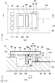
- FIGS. 1 (A) and 1 (B) in which the same reference numerals are assigned to the corresponding parts to FIGS. 26 (A) and (B), 1 is the first embodiment according to the present invention.
- the signal transmission apparatus of the form is shown.
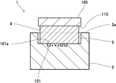
- the signal transmission device 1 is provided with the optical waveguide 101 on the surface 2a of the base 2. It has a feature that it has an exposed optical waveguide portion 5 with an exposed peripheral surface portion 101a, and a spacer 4 is provided on the exposed optical waveguide portion 5.
- the spacer 4 is interposed between the peripheral surface portion 101 a of the optical waveguide 101 and the back surface 115 of the optical module substrate 105 in the optical waveguide exposed portion 5, and has a height facing the optical waveguide end surface 109.
- the optical waveguide exposed portion 5 is a predetermined position between the concave portion 107 of the base 2 and the guide pin hole 110, and the region between the surface 2a of the base 2 and the optical waveguide 101 is notched. It is formed to be.
- the optical waveguide exposed portion 5 has a rectangular parallelepiped shape, and is formed so that the peripheral surface portion 101 a of the optical waveguide 101 can be exposed from the surface 2 a of the base 2.
- the optical waveguide exposed portion 5 has a width dimension in which the spacer 4 supporting the optical module substrate 105 can be installed inside, and as shown in FIG. 2 showing a BB ′ cross section of FIG. The depth dimension is formed such that the spacer 4 can be installed.
- the concave portion 107 is formed.
- An uncut remaining portion 6 may be provided on the surface between the side surface portion 108 and the optical waveguide exposed portion 5.
- the peripheral surface portion 101a of the optical waveguide 101 extends between the installation location of the spacer 4 and the optical waveguide end surface 109. Is exposed, there is a possibility that the peripheral surface portion 101a of the optical waveguide 101 is chipped because the exposed optical waveguide 101 is directly polished in the polishing process for forming the optical waveguide end surface 109. There arises a problem that it is difficult to form the optical waveguide end face 109 flat.
- the spacer 4 has a rectangular parallelepiped shape, and its upper end is joined to the back surface 115 of the optical module substrate 105 by the joining member 8.
- the optical waveguide of the base 2 It can be arranged in the exposed portion 5.
- the spacer 4 has an outer peripheral shape that is substantially the same as the optical waveguide exposed portion 5 and is slightly smaller than the outer peripheral shape of the optical waveguide exposed portion 5. ing.
- the spacer 4 adjusts a distance L5 from the back surface 115 of the optical module substrate 105 to the peripheral surface portion 101a of the optical waveguide 101, and the center of the optical waveguide 101 is the optical element 103.
- a dimension in the thickness direction z (hereinafter referred to as a height dimension) is selected so as to face the light receiving area and the light emitting area. That is, the height of the spacer 4 is such that the total distance combined with the distance L4 from the peripheral surface portion 101a of the optical waveguide 101 to the center thereof is from the back surface 115 of the optical module substrate 105 to the light receiving region and the light emitting region of the optical element 103. It is selected to be the same as the distance L1.
- FIG. 3 (A) and FIG. 3 (B) showing the CC ′ cross section of FIG. 3 (A) a plurality of layers are bonded with an adhesive or the like according to the manufacturing process of the FR4 printed circuit board.
- a processing base 10 in which a plurality of optical waveguides 101 are arranged in parallel is manufactured.
- a polishing margin in which the optical waveguide 101 extends to the recess formation region in order to form a flat optical waveguide end surface 109 (FIG. 1B) later by polishing processing. M1 is formed.
- a flat optical waveguide end surface 109 is formed on the processing base 10 by polishing the side surface portion 108 of the recess 107.
- FIG. 5 (A) and FIG. 5 (B) showing the EE ′ cross section of FIG. 5 (A) a predetermined distance from the recess 107 is applied to the surface by the same processing method as the cavity substrate.
- the base 2 can be manufactured by forming the optical waveguide exposed portion 5 where the peripheral surface portion 101 a of the optical waveguide 101 is exposed and the remaining portion 6.
- the spacer 4 provided on the back surface 115 of the optical module substrate 105 is disposed in the optical waveguide exposed portion 5, and the guide pin hole 114 of the optical module substrate 105 and the base
- the signal transmission device 1 can be manufactured by inserting the guide pin 111 into the guide pin hole 110 of the base 2 and joining the base 2 and the optical module substrate 105 with the joining member 117 in this state.
- the surface 2 a of the base 2 is selectively removed at a predetermined distance from the optical waveguide end face 109 of the base 2, and the peripheral surface portion 101 a of the optical waveguide 101 is the base 2.
- An optical waveguide exposed portion 5 exposed from the surface 2a is formed.
- the spacer 4 is inserted between the peripheral surface portion 101 a of the optical waveguide 101 exposed in the optical waveguide exposed portion 5 and the back surface 115 of the optical module substrate 105, and the height of the spacer 4 is determined. The distance from the back surface 115 of the optical module substrate 105 to the optical waveguide 101 is adjusted only by the dimensions.
- the height of the optical element 103 provided on the optical module substrate 105 is opposed to the optical waveguide end surface 109 by simply adjusting the height of the spacer 4 with the optical waveguide 101 as a reference at all times.
- the optical waveguide exposed portion 5 is formed at a predetermined distance from the side surface portion 108 of the recess 107, and the remaining portion is provided between the side surface portion 108 of the recess 107 and the optical waveguide exposed portion 5.
- 6 is provided so that the peripheral surface portion 101a of the optical waveguide 101 is not exposed, so that the peripheral surface portion 101a of the optical waveguide 101 can be prevented from being chipped during polishing, and thus a flat optical waveguide end surface 109 can be formed.
- this signal transmission device 1 since the remaining portion 6 is provided between the support portion 113 and the spacer 4 and a predetermined space is formed above the remaining portion 6, the support portion 113 and the spacer 4.
- the extra joining member 8 that protrudes from the joint between the optical module substrate 105 and the optical module substrate 105 can be released into the space.
- the spacer 4 is interposed between the peripheral surface portion 101a of the optical waveguide 101 exposed at the optical waveguide exposed portion 5 and the back surface 115 of the optical module substrate 105, and only the height dimension of the spacer 4 is concerned.
- the optical element 103 of the optical module substrate 105 it is not necessary to individually produce a spacer for each signal transmission device, and the optical waveguide from the surface 2a of the base 2
- Individual length measurement such as the distance L2 to the peripheral surface 101a of 101 can be omitted, thus improving the production efficiency of the product and reducing the production cost by eliminating the need for the length measurement process and length measurement device. Can be planned.
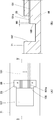
- FIGS. 6 (A) and 6 (B) the parts corresponding to those in FIGS. 1 (A) and 1 (B) are denoted by the same reference numerals, and 21 is according to the second embodiment.
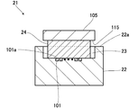
- the signal transmission device is shown, and the position of the optical waveguide exposure portion 23 formed on the base 22 and the installation position of the spacer 24 are different from those of the first embodiment.
- the base 22 has the remaining portion 6 (FIG. 6) in the first embodiment. 1 (B)) is not formed, and the optical waveguide exposed portion 23 is formed adjacent to the recess 107.
- the optical waveguide exposed portion 23 is the same as the optical waveguide exposed portion 5 (FIG. 1B) of the first embodiment except that it is formed so as to be adjacent to the concave portion 107.
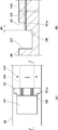
- the exposed portion 23 of the optical waveguide has a width dimension in which a rectangular parallelepiped spacer 24 can be installed, and the depth dimension thereof is the spacer 24 as shown in FIG. 7 showing a section GG ′ in FIG. It is formed in the dimension that can be installed.
- the spacer 24 is formed of a harder member than the optical waveguide 101 or the base 22, such as ceramic or metal (copper, aluminum), for example.
- the one side surface 24a is configured not to be reduced by polishing performed when forming the film. Thereby, the spacer 24 has a role of a stopper because the one side surface 24a is not cut during the polishing process for processing the optical waveguide end surface 109 to be flat, and the optical waveguide end surface 109 is flush with the flat one side surface 24a. Can be formed.
- the spacer 24 is the same as the spacer 4 (FIG. 1B) of the first embodiment except for the configuration described above.
- FIG. 8A and FIG. 8B showing the HH ′ cross section of FIG. 8A
- a plurality of layers are bonded with an adhesive or the like according to the manufacturing process of the FR4 printed circuit board.
- a processing base 26 in which a plurality of optical waveguides 101 are arranged in parallel is manufactured.
- the processing base 26 is formed with a polishing margin M1 in which the optical waveguide 101 extends to the recess formation region in order to form the flat optical waveguide end surface 109 by the subsequent polishing processing. .
- the processing base 26 is an area adjacent to the recess 107 as shown in FIG. 10A and FIG. 10B showing the JJ ′ cross section of FIG.
- the optical waveguide exposed portion 23 in which the peripheral surface portion 101a of the optical waveguide 101 is exposed from the surface is formed.
- the optical waveguide exposed portion 23 has a rectangular parallelepiped shape and communicates with the concave portion 107, and a polishing margin M1 having a predetermined width dimension is provided at the bottom.
- the polishing margin is formed on the peripheral surface portion 101a of the optical waveguide 101 exposed at the optical waveguide exposed portion 23.
- M1 is provided and the spacer 24 is placed, and the spacer 24 is fixed to the optical waveguide exposed portion 23 by the bonding member 28 in this state.
- the polishing margin M1 is polished in the region adjacent to the one side surface 24a of the spacer 24, the optical waveguide end surface 109 is formed on the side surface portion 108 of the recess 107, and thus the base 22 can be manufactured. Yes.
- the spacer 24 is formed of a harder member than the optical waveguide 101 and the base 22, and is difficult to polish by polishing.
- the side surface 24a plays the role of a stopper without being cut, and as shown in FIG. 12 (A) and FIG. 12 (B) showing the LL ′ cross section of FIG.
- the optical waveguide end face 109 can be formed flush.
- the guide pin 111 is inserted into the guide pin hole 114 of the optical module substrate 105 and the guide pin hole 110 of the base 2, and the upper end portion of the spacer 24 is joined to the joining member 29.
- 117 can be used to manufacture the signal transmission device 21.
- the spacer 24 is interposed between the peripheral surface portion 101a of the optical waveguide 101 exposed at the optical waveguide exposed portion 23 and the back surface 115 of the optical module substrate 105, and the spacer 24 The distance from the back surface 115 of the optical module substrate 105 to the optical waveguide 101 is adjusted only by the height dimension.
- the height of the optical element 103 provided on the optical module substrate 105 is opposed to the optical waveguide end surface 109 by simply adjusting the height of the spacer 24 with the optical waveguide 101 as a reference at all times.
- the spacer 24 when the spacer 24 is formed of a harder member than the optical waveguide 101 or the base 22, and the optical waveguide end surface 109 is formed by polishing processing, the polishing processing is performed.
- the side surface 24a of the spacer 24 is not cut, and the spacer 24 serves as a stopper for regulating the polishing range, so that the optical waveguide end surface 109 is flush with the side surface 24a of the spacer 24.
- the optical waveguide end surface 109 can be accurately formed by polishing to match the one side surface 24a of the spacer 24. Therefore, the gap ⁇ L2 between the optical element 103 and the optical waveguide end surface 109 is increased for each production. It can prevent variation.
- the optical waveguide end surface 109 of the base 102 is formed by polishing, and the optical waveguide end surface 109 with respect to the position of the guide pin hole 110 is formed.
- the position contains a certain error.
- the gap ⁇ L1 between the optical element 103 and the optical waveguide end face 109 is likely to vary from production to production, resulting in production variations in optical coupling efficiency and a decrease in yield. It was.
- the optical coupling efficiency between the optical element 103 and the optical waveguide 101 is low, in the optical transmission path from the optical transmission element (optical element) to the optical light receiving element (optical element) via the optical waveguide 101, each gap ⁇ L1 As a result of the increase, the optical loss occurs at each optical coupling point, and the light receiving level at the optical receiving element decreases. For this reason, in order to compensate for the loss, the optical transmission element needs to increase the optical output level accordingly, and there is a problem that the power consumption increases as the drive current increases.
- the spacer 24 is accurately placed at a predetermined position, and polishing is performed in this state, so that the light is aligned with the one side surface 24a of the spacer 24. Since the waveguide end face 109 is formed, it is possible to prevent the distance from the position of the guide pin hole 110 to the position of the optical waveguide end face 109 from being varied for each production due to polishing. Thereby, in this signal transmission device 21, the gap ⁇ L2 between the optical element 103 and the optical waveguide end face 109 can be kept constant, so that the optical coupling efficiency between the optical element 103 and the optical waveguide end face 109 can be improved. And the yield can be improved.
- the gap ⁇ L2 between the optical element 103 and the optical waveguide end face 109 can be maintained constant, optical loss due to variation in the gap ⁇ L2 is less likely to occur in the optical coupling between the optical element 103 and the optical waveguide 101. It is possible to reduce power consumption set in consideration of optical loss in an optical element that is an optical transmission element.
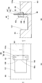
- FIGS. 13 (A) and 13 (B) in which parts corresponding to those in FIGS. 6 (A) and 6 (B) are denoted by the same reference numerals, 31 denotes the third embodiment.
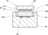
- a signal transmission device is shown, which differs from the second embodiment in that a stepped portion 33 is formed on one side surface of the spacer 32.
- the spacer 32 forms a relief space G1 with a recessed step portion 33 on one side, and is supported.
- An extra joining member 29 that protrudes from the joining portion between the portion 113 or the spacer 32 and the optical module substrate 105 is configured to escape into the escape space G1.
- the spacer 32 is composed of a first spacer portion 34 fixed to the peripheral surface portion 101a of the optical waveguide 101 exposed at the optical waveguide exposed portion 23, and the first spacer portion 34, and is separated from the first spacer portion 34.
- the second spacer portion 35 is interposed between the spacer portion 34 and the back surface 115 of the optical module substrate 105.
- the present invention is not limited to this, and the first A spacer in which the spacer portion and the second spacer portion are integrally formed may be applied.
- the spacer 32 is formed between the peripheral surface portion 101a of the optical waveguide 101 exposed at the optical waveguide exposed portion 23 and the back surface 115 of the optical module substrate 105, as shown in FIG.
- the height dimension of the first spacer portion 34 and the second spacer portion 35 is selected so that the center of the optical waveguide 101 faces the light receiving region and the light emitting region of the optical element 103. Has been. Thereby, the spacer 32 can obtain the same effect as that of the second embodiment described above.
- the first spacer portion 34 has a rectangular parallelepiped shape, is formed of a harder member than the optical waveguide 101 and the base 22, and is not reduced by polishing performed when the optical waveguide end surface 109 is formed. It is configured. As a result, the first spacer portion 34 has a role of a stopper since the one side surface 34a is not cut during the polishing process for processing the optical waveguide end face 109 to be flat, and the optical waveguide is flush with the one side surface 34a. An end face 109 can be formed.
- the second spacer portion 35 is formed of various other members such as the same hard member as the first spacer portion 34 or the same member as the base 22.
- the second spacer portion 35 has a rectangular parallelepiped shape, and the dimension (width dimension) in the width direction x is selected to be shorter than the width dimension of the first spacer part 35.
- the second spacer portion 35 is disposed so that one side surface 35a faces the support portion 113 when disposed at the upper end portion of the first spacer portion 34, as shown in FIG. 13B.
- the other side surface 35b facing the one side surface 35a is arranged flush with the other side surface 34b of the first spacer portion 34.
- the spacer 32 is formed with a stepped portion 33 that is recessed at the boundary between the one side surface 34a of the first spacer portion 34 and the one side surface 35a of the second spacer portion 35, and the stepped portion 33 forms the second spacer.
- a clearance space G1 may be formed between the portion 35 and the support portion 113.
- the spacer 32 is formed at the location adjacent to the optical module substrate 105 by forming a clearance space G1 between the second spacer portion 35 facing the support portion 113, and thereby the support portion 113 and the second spacer. Even if a part of the joining member 29 used when fixing the portion 35 to the back surface 115 of the optical module substrate 105 protrudes, the excess joining member 29 that protrudes can escape to the escape space G1.
- the other side surface 34b of the first spacer portion 34 and the other side surface 35b of the second spacer portion 35 are arranged flush with each other, whereby one side surface of the first spacer portion 34 is arranged.
- the present invention is not limited to this, and the other side surface 34b of the first spacer portion 34,
- the other side surface 35b of the second spacer portion 35 may be provided with a step, and in short, is recessed at the boundary between the one side surface 34a of the first spacer portion 34 and the one side surface 35a of the second spacer portion 35. It is only necessary that the stepped portion 33 can be formed.
- the manufacturing method of the base 22 according to the third embodiment is the same as the manufacturing method of the base 22 according to the second embodiment. That is, in FIG. 11 and FIG. 12, the base 22 in which the optical waveguide end face 109 is formed flush with the one side surface 34a of the first spacer portion 34 by replacing the spacer 24 with the first spacer portion 34. Can be manufactured.
- the third embodiment when the optical module substrate 105 is bonded to the base 22, one side surface 34a of the first spacer portion 34 and one side surface of the second spacer portion 35 are provided.
- the second spacer portion 35 is joined to the back surface 115 of the optical module substrate 105 by the joining member 29 so that a stepped portion 33 that is recessed at the boundary with 35a is formed. Then, as shown in FIG.
- the optical module substrate The signal transmission device 31 is manufactured by inserting the guide pin 111 into the guide pin hole 114 of 105 and the guide pin hole 110 of the base, and joining the base 22 and the optical module substrate 105 with the joining member 117. Can do.
- the signal transmission device 31 can obtain the same effect as that of the second embodiment described above, and can be supported on the first spacer portion 34 even if the support portion 113 and the spacer 32 are close to each other.
- the relief space G1 is formed in the region where the portion 113 and the second spacer portion 35 are opposed to each other, so that the excess joining that protrudes from the joining portion with the optical module substrate 105 in the support portion 113 and the second spacer portion 35 is performed.
- the member 29 can escape to the escape space G1.
- the first spacer portion 34 can maintain a predetermined width dimension while forming the escape space G1, and thus can be stably installed on the bottom portion of the optical waveguide exposed portion 23.
- the spacer 24 in the second embodiment and the first spacer portion 34 in the third embodiment are optically flush with the side surfaces 24a and 34a.
- the spacer 24 and the first spacer portion 34 can be accurately installed on the optical waveguide exposed portion 23. .
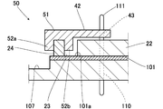
- the spacer installation jig 40 is formed of a plate-like member having a predetermined thickness, and includes an installation part 41 formed thicker and a positioning part 42 formed thinner than the installation part 41. It has an integrally formed configuration.
- the positioning portion 42 has a pin insertion hole 43 formed at a position facing the guide pin hole 110 formed in the base 22 when the spacer installation jig 40 is disposed above the base 22.
- the guide pin 111 can be inserted into the pin insertion hole 43.
- the spacer installation jig 40 can be accurately positioned with respect to the base 22 by inserting the guide pin 111 inserted into the guide pin hole 110 of the base 22 into the pin insertion hole 43 of the positioning portion 42. It is configured as follows.
- the installation portion 41 integrally formed with the positioning portion 42 has, for example, substantially the same shape as the outer periphery of the spacer 24, and has a through hole 44 selected slightly larger than the spacer 24.
- the through hole 44 is formed so as to face a predetermined position of the optical waveguide exposed portion 23 where the spacer 24 is disposed when the positioning portion 42 is positioned with respect to the base 22 by the guide pin 111.
- the installation portion 41 moves the spacer 24 along the through hole 44 when the spacer 24 is inserted into the through hole 44 from above.
- the spacer 24 is dropped as it is, and the spacer 24 can be accurately placed at a predetermined position of the optical waveguide exposed portion 23.
- the spacer 24 can be joined to the optical waveguide exposed portion 23 by the joining member.
- the guide pin 111 provided on the base 22 is simply inserted into the pin insertion hole 43 of the spacer installation jig 40, so that the installation portion 41 can be accurately positioned, and in this state, the spacer 24 can be accurately installed on the optical waveguide exposed portion 23 only by inserting the spacer 24 into the through hole 44 of the installation portion 41 and dropping it. Therefore, the manufacturing method using the spacer installation jig 40 is optimal for automation of the manufacturing process and is suitable for mass production.
- reference numeral 50 denotes a spacer installation jig according to another embodiment, and the configuration of the installation part 51 is different from the spacer installation jig 40 described above.
- the spacer installation jig 50 has an installation portion 51 formed in a U-shaped cross section, and is configured to sandwich the spacer 24 between projections 52a and 52b protruding from the lower surface of the installation portion 51.
- the spacer installation jig 50 is inserted into the pin insertion hole 43 of the positioning portion with the spacer 24 sandwiched between the protrusions 52a and 52b as shown in FIG. 18 showing the PP ′ cross section of FIG.
- the guide pin 111 is inserted and positioned, approaches the base 22 along the guide pin 111, and places the spacer 24 held between the protruding portions 52a and 52b at a predetermined position of the optical waveguide exposed portion 23. .
- the installation unit 51 joins the spacer 24 to the optical waveguide exposed part 23 by using, for example, a joining member, and then moves the spacer installation jig 50 itself along the guide pin 111 to move the protrusions 52a and 52b between The spacer 24 can be removed from the.
- the spacer installation jig 50 is used as described above, the guide pin 111 provided on the base 22 is simply inserted into the pin insertion hole 43 of the spacer installation jig 50 and the spacer 24 is inserted into the base 22. Can be positioned accurately.
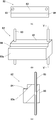
- FIGS. 19 (A) and 19 (B) in which the same reference numerals are given to the corresponding parts to FIGS. 6 (A) and 6 (B), 61 is according to the fourth embodiment.
- a signal transmission device is shown and differs from the above-described second embodiment in that a spacer 64 with a pin provided with a guide pin 63 is applied to a spacer body 62.
- the base 65 is provided with the optical waveguide 101 at the bottom of the optical waveguide exposed portion 23.
- Guide pin holes 66 penetrating the thickness are formed on both sides so as to avoid, and the guide pin 63 protruding from the lower end of the pin-attached spacer 64 can be inserted into the guide pin hole 66.
- the optical module substrate 68 is provided with a guide pin hole 67 penetrating through a thickness at a position facing the guide pin hole 66 of the base 65 when positioned with respect to the base 65, A guide pin 63 protruding from the upper end of the pin spacer 64 can be inserted into the guide pin hole 67.
- the base 65 has an optical waveguide end surface 109 flush with the one side surface 62a of the spacer main body 62 of the spacer 64 with the pin, and the optical waveguide end surface 109 is between the optical element 103 of the optical module substrate 68.
- the optical waveguide 101 and the optical element 103 can be optically coupled to each other with a predetermined gap ⁇ L2 therebetween.
- two guide pins 63 are arranged at intervals in a spacer body 62 formed in a rectangular parallelepiped shape.
- the guide pins 63 are provided so that the front ends thereof can protrude from the upper end portion and the lower end portion of the spacer body 62, respectively.
- the spacer main body 62 and the guide pin 63 are configured separately as shown in FIG. 20C showing the RR ′ cross section of FIG. 20B.
- the invention is not limited to this, and the spacer main body and the guide pin may be integrally formed.
- the spacer main body 62 is formed of a member that is harder than the optical waveguide 101 or the base 65, such as ceramic or metal (copper, aluminum), for example, and is formed when the optical waveguide end face 109 is formed.
- the one side surface 62a is not reduced by the polishing process.
- the spacer main body 62 has a role of a stopper because the one side surface 62a is not cut during polishing for processing the optical waveguide end surface 109 to be flat, and the optical waveguide end surface is flush with the flat one side surface 62a. 109 can be formed.
- the height dimension of the spacer body 62 (that is, the distance L5) is such that the total distance combined with the distance L4 from the peripheral surface portion 101a to the center of the optical waveguide 101 is from the back surface 69 of the optical module substrate 68 to It is selected to be the same as the distance L1 to the light emitting area.
- FIG. 21 (A) and FIG. 21 (B) showing the SS ′ cross section of FIG. A part of the surface is removed to form a rectangular parallelepiped concave portion 107.
- the recess 107 is provided with a polishing margin M1 having a predetermined width dimension on the side surface 108.
- the processing base 71 is subjected to router processing on the region adjacent to the recess 107 and above the peripheral surface portion 101a of the optical waveguide 101, so that light is transmitted from the surface of the processing base 71.
- An optical waveguide exposed portion 23 in which the peripheral surface portion 101a of the waveguide 101 is exposed is formed.
- the optical waveguide exposed portion 23 has a rectangular parallelepiped shape and communicates with the recess 107, and a polishing margin M1 having a predetermined width dimension is provided as it is at the bottom.
- a guide pin hole 66 that penetrates the thickness is formed at a predetermined position on both sides of the optical waveguide 101 so as to avoid the optical waveguide 101 at the bottom of the optical waveguide exposed portion 23.
- the lower end portion of the pinned spacer 64 is inserted into the guide pin hole 66 of the exposed portion 23 of the optical waveguide.
- the spacer main body 62 is positioned on the peripheral surface portion 101a of the optical waveguide 101 exposed at the optical waveguide exposed portion 23 by inserting the guide pin 63 protruding from the optical waveguide, and the spacer main body 62 is moved by the bonding member 28 in this state. Fix to the exposed part 23. At this time, the spacer main body 62 is installed on the optical waveguide exposed portion 23 with a polishing margin M1.
- the polishing margin M1 in the region adjacent to the side surface 62a of the spacer body 62 is polished.
- the optical waveguide end face 109 is formed on the side face 108 of the recess 107.
- the spacer main body 62 is formed of a hard member compared to the optical waveguide 101 and the base 65 and is difficult to polish by polishing.
- the one side surface 62a of the main body 62 serves as a stopper without being cut, and the optical waveguide end face 109 can be formed flush with the one side surface 62a of the spacer main body 62.
- the guide pin 63 protruding from the upper end of the pin spacer 64 installed on the base 65 is inserted into the guide pin hole 67 drilled in the optical module substrate 68, and thereby the optical module substrate 68 with respect to the base 65.
- the signal transmission device 61 shown in FIGS. 19A and 19B can be manufactured.
- the spacer main body 62 is inserted between the peripheral surface portion 101a of the optical waveguide 101 exposed at the optical waveguide exposed portion 23 and the back surface 69 of the optical module substrate 68, and the spacer The distance from the back surface 69 of the optical module substrate 68 to the optical waveguide 101 is adjusted only by the height dimension of the main body 62.
- the height of the optical element 103 provided on the optical module substrate 68 is opposed to the optical waveguide end surface 109 by simply adjusting the height of the spacer body 62, always using the optical waveguide 101 as a reference. Can be adapted. Therefore, in the signal transmission device 61, even if the distance L2 from the surface 65a of the base 65 to the peripheral surface portion 101a of the optical waveguide 101 changes for each production, the thickness is increased by the spacer body 62 selected in advance to a predetermined height. In the vertical direction z, the optical element 103 can be optically coupled to the optical waveguide end face 109 with certainty.
- the spacer main body 62 when the spacer main body 62 is formed of a harder member than the optical waveguide 101 and the base 65, and the optical waveguide end surface 109 is formed by polishing, the spacer main body 62 is obtained by the polishing.
- the optical waveguide end surface 109 is formed flush with the one side surface 62a of the spacer main body 62 by making the spacer main body 62 act as a stopper for regulating the polishing range without cutting the one side surface 62a of the optical waveguide. can do.
- the optical waveguide end surface 109 can be accurately formed by polishing to match the one side surface 62a of the spacer main body 62. Therefore, the gap ⁇ L2 between the optical element 103 and the optical waveguide end surface 109 is increased every production It is possible to prevent scatter.
- the spacer body 62 since the spacer body 62 itself is provided with the guide pin 63, the guide pin hole 66 formed in the optical waveguide exposed portion 23 By inserting the guide pin 63, the spacer body 62 can be accurately positioned with respect to the optical waveguide exposed portion. Therefore, in this signal transmission device 61, the optical waveguide end surface 109 flush with the one side surface 62a of the spacer main body 62 is formed by polishing, so that the base 65 is aligned with the position of the one side surface 62a of the spacer main body 62. On the other hand, the optical waveguide end face 109 can be accurately formed.
- the tip of the guide pin 63 is formed so as to protrude also at the upper end portion of the spacer 64 with the pin, and the guide pin 63 protruding from the upper end portion of the spacer body 62 is connected to the optical module substrate 68.
- the optical module substrate 68 can be accurately positioned with respect to the base 65. Therefore, in this signal transmission device 61, a separate guide pin is prepared separately from the pin spacer 64, and the installation work of the base 65 and the optical module board 68 using the guide pin is separately performed separately from the spacer installation work. The labor to perform can be saved and the manufacturing operation can be simplified.
- FIG. 24 in which parts corresponding to those in FIG. 19B are assigned the same reference numerals, 81 denotes a signal transmission apparatus according to the fifth embodiment.
- This embodiment is different from the embodiment in that a stepped portion 84 is formed in the spacer main body 83 of the spacer 82 with the pin.
- the spacer main body 83 in the vicinity of the back surface 69 of the optical module substrate 68, the spacer main body 83 has a stepped portion 84 formed by cutting a part of one side surface 83a facing the support portion 113 into a thin shape. ing.
- the spacer body 83 forms a clearance space G1 by the stepped portion 84, and the excess joining member 29 that protrudes from the joint portion with the optical module substrate 68 in the support portion 113 or the spacer body 83 is allowed to escape to the clearance space G1. It is configured as follows.
- the signal transmission device 81 can obtain the effects of the above-described fourth embodiment and also the effects of the third embodiment.
- the present invention is not limited to this embodiment, and various modifications can be made within the scope of the gist of the present invention.
- the spacer is applied, the present invention is not limited to this, and for example, a spacer with a pin in which a guide pin is integrally formed with a spacer main body as in the fourth embodiment may be applied.
- the escape space is provided by forming the step portion in the spacer
- the present invention is not limited to this, You may make it provide relief space by providing the concave of various shapes, such as curved shape, in a spacer.
- the guide pins 63 protrude from the upper and lower ends of the spacer bodies 62 and 83, and the spacer bodies 62 and 83 are positioned on the base 65 and the optical module substrate 68.
- the present invention is not limited to this, and the guide pin protrudes only at either the upper end or the lower end of the spacer body, and the spacer body is provided on either the base or the optical module substrate. It may be positioned.
Landscapes
- Physics & Mathematics (AREA)
- General Physics & Mathematics (AREA)
- Optics & Photonics (AREA)
- Optical Couplings Of Light Guides (AREA)
- Optical Integrated Circuits (AREA)
Abstract
Description
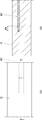
図26(A)及び(B)との対応部分に同一符号を付して示す図1(A)及び(B)において、1は本発明による第1の実施の形態の信号伝送装置を示す。ここで、図1(A)と、図1(A)のA-A´断面を示す図1(B)のように、この信号伝送装置1は、基台2の表面2aに光導波路101の周面部101aが露出した光導波路露出部5を有し、この光導波路露出部5にスペーサ4が設けられている点を特徴としている。
図1(A)及び(B)との対応部分に同一符号を付して示す図6(A)及び(B)において、21は第2の実施の形態による信号伝送装置を示し、第1の実施の形態とは基台22に形成される光導波路露出部23の位置と、スペーサ24の設置位置とが相違する。
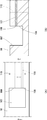
図6(A)及び(B)との対応部分に同一符号を付して示す図13(A)及び(B)において、31は第3の実施の形態による信号伝送装置を示し、第2の実施の形態とはスペーサ32の一側面に段差部33が形成されている点で相違する。図13(A)と、図13(A)のM-M´断面を示す図13(B)のように、スペーサ32は、一側面の凹んだ段差部33によって逃げ空間G1を形成し、支持部113又はスペーサ32と光モジュール基板105との接合箇所からはみ出た余分な接合部材29を、この逃げ空間G1へ逃がすように構成されている。
105のガイドピン孔114と、基台のガイドピン孔110とにガイドピン111を挿通し、これら基台22と光モジュール基板105とを接合部材117により接合することにより、信号伝送装置31を製造し得る。
ここで、上述した第2の実施の形態におけるスペーサ24や、第3の実施の形態における第1のスペーサ部34は、各一側面24a,34aと面一に光導波路端面109を形成させるため、製造工程において、光導波路端面109が形成される位置に対し正確に設置する必要がある。そこで、図15(A)及び(B)に示すようなスペーサ設置治具40を用いることにより、スペーサ24や第1のスペーサ部34を光導波路露出部23に対して正確に設置させることができる。
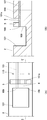
図6(A)及び(B)との対応部分に同一符号を付して示す図19(A)及び(B)において、61は第4の実施の形態による信号伝送装置を示し、上述した第2の実施の形態とはスペーサ本体62にガイドピン63が設けられたピン付スペーサ64を適用した点で相違する。図19(A)と、図19(A)のQ-Q´断面を示す図19(B)のように、この基台65には、光導波路露出部23の底部であって光導波路101を避けるように両側部に厚みを貫通したガイドピン孔66が穿設され、ピン付スペーサ64の下端部から突出したガイドピン63が当該ガイドピン孔66に挿入され得る。また、光モジュール基板68には、基台65に対して位置決めされた際に、当該基台65のガイドピン孔66と対向する位置に厚みを貫通したガイドピン孔67が穿設されており、ピン付スペーサ64の上端部から突出したガイドピン63が当該ガイドピン孔67に挿入され得る。
ガイドピン孔66が穿設される。
図19(B)との対応部分に同一符号を付して示す図24において、81は第5の実施の形態による信号伝送装置を示し、上述した第4の実施の形態とはピン付スペーサ82のスペーサ本体83に段差部84が形成されている点で相違する。この場合、スペーサ本体83は、光モジュール基板68の裏面69近傍付近において、支持部113と対向する一側面83aの一部が切り欠かれて薄肉状に形成されることにより段差部84が形成されている。これによりスペーサ本体83は、段差部84によって逃げ空間G1を形成し、支持部113又はスペーサ本体83において光モジュール基板68との接合箇所からはみ出た余分な接合部材29を、この逃げ空間G1へ逃がすように構成されている。
なお、本発明は、本実施形態に限定されるものではなく、本発明の要旨の範囲内で種々の変形実施が可能であり、例えば第1の実施の形態においてスペーサを適用したが、本発明はこれに限らず、例えば第4の実施の形態のようにスペーサ本体にガイドピンを一体成形させたピン付スペーサを適用してもよい。
2,22,65 基台
105,68 光モジュール基板
4,24,32 スペーサ
5,23 光導波路露出部
64,82ピン付スペーサ(スペーサ)
63 ガイドピン
101 光導波路
103 光素子
Claims (10)
- 光信号が伝送する光導波路が内部に形成され、前記光導波路の端面が露出した基台と、前記光信号を送信又は受信する光素子を前記基台の表面と対向する裏面に有する光モジュール基板とを備え、前記光導波路の端面と前記光素子とが対向して光結合する信号伝送装置であって、
前記基台は、
前記表面から前記光導波路の周面部を露出させる光導波路露出部と、
前記光導波路露出部に露出した前記光導波路の周面部と、前記光モジュール基板の裏面との間に介挿され、前記光導波路の端面に対向する高さに前記光素子を合わせるスペーサとを備える
ことを特徴とする信号伝送装置。 - 前記光導波路の端面から前記光導波路露出部までの間は、前記光導波路が前記基台の内部に形成され、前記光導波路の周面部が非露出状態である
ことを特徴とする請求項1記載の信号伝送装置。 - 前記スペーサは前記基台及び前記光導波路よりも硬質な部材により形成されており、
前記スペーサの一側面に対して前記光導波路の端面が面一に形成されている
ことを特徴とする請求項1記載の信号伝送装置。 - 前記光素子を支持する支持部と、前記スペーサの上端部とが前記光モジュール基板の裏面に接合部材により接合されており、
前記光導波路の端面と面一となる前記スペーサの一側面には、前記支持部又は前記スペーサの接合箇所からはみ出た余分な接合部材を逃がす逃げ空間が形成されている
ことを特徴とする請求項3記載の信号伝送装置。 - 少なくとも前記基台又は前記光モジュール基板のいずれかに、ガイドピン孔が穿設されており、
前記スペーサには、前記基台又は前記光モジュール基板のいずれかの前記ガイドピン孔に挿通し、前記基台又は前記光モジュール基板に前記スペーサを位置決めさせるためのガイドピンが設けられている
ことを特徴とする請求項1~4のうちいずれか1項記載の信号伝送装置。 - 光信号が伝送する光導波路が内部に形成され、前記光導波路の端面が露出した基台と、
前記光信号を送信又は受信する光素子を前記基台の表面と対向する裏面に有する光モジュール基板とを備え、前記光導波路の端面と前記光素子とが対向して光結合する信号伝送装置の製造方法であって、
前記基台の表面から前記光導波路の周面部が露出した光導波路露出部を形成する露出部形成ステップと、
前記光導波路露出部に露出した前記光導波路の周面部と、前記光モジュール基板の裏面との間にスペーサを介挿し、前記スペーサによって、前記光導波路の端面に対向する高さに前記光素子を合わせるスペーサ設置ステップと
を備えることを特徴とする信号伝送装置の製造方法。 - 前記露出部形成ステップは、
前記光導波路の端面から前記光導波路露出部までの間において、前記光導波路が前記基台の内部に形成され、前記光導波路の周面部が非露出状態である
ことを特徴とする請求項6記載の信号伝送装置の製造方法。 - 前記スペーサ設置ステップで用いられる前記スペーサは前記基台及び前記光導波路よりも硬質な部材により形成されており、
前記スペーサ設置ステップの後に、前記スペーサの一側面に対して前記光導波路の端面を面一に形成する加工ステップを備える
ことを特徴とする請求項6記載の信号伝送装置の製造方法。 - 前記スペーサ設置ステップで用いられる前記スペーサには、前記光導波路の端面と面一となる一側面に逃げ空間が形成されており、
前記光素子を支持する支持部と、前記スペーサの上端部とが前記光モジュール基板の裏面に接合部材により接合された際に、前記支持部又は前記スペーサの接合箇所からはみ出た余分な接合部材が前記逃げ空間に逃げる
ことを特徴とする請求項8記載の信号伝送装置の製造方法。 - 前記スペーサ設置ステップの前に、少なくとも前記基台又は前記光モジュール基板のいずれかに、ガイドピン孔を穿設する穿設ステップを備え、
前記スペーサ設置ステップで用いる前記スペーサには、前記基台又は前記光モジュール基板のいずれかの前記ガイドピン孔に挿通可能なガイドピンが設けられており、
前記スペーサ設置ステップでは、前記基台又は前記光モジュール基板に前記ガイドピンによって前記スペーサを位置決めさせる
ことを特徴とする請求項6~9記載のうちいずれか1項記載の信号伝送装置の製造方法。
Priority Applications (2)
| Application Number | Priority Date | Filing Date | Title |
|---|---|---|---|
| JP2011504855A JPWO2010107044A1 (ja) | 2009-03-17 | 2010-03-17 | 信号伝送装置及びその製造方法 |
| US13/256,802 US20120002923A1 (en) | 2009-03-17 | 2010-03-17 | Signal transmission device and manufacturing method therefor |
Applications Claiming Priority (2)
| Application Number | Priority Date | Filing Date | Title |
|---|---|---|---|
| JP2009-065271 | 2009-03-17 | ||
| JP2009065271 | 2009-03-17 |
Publications (1)
| Publication Number | Publication Date |
|---|---|
| WO2010107044A1 true WO2010107044A1 (ja) | 2010-09-23 |
Family
ID=42739704
Family Applications (1)
| Application Number | Title | Priority Date | Filing Date |
|---|---|---|---|
| PCT/JP2010/054496 Ceased WO2010107044A1 (ja) | 2009-03-17 | 2010-03-17 | 信号伝送装置及びその製造方法 |
Country Status (3)
| Country | Link |
|---|---|
| US (1) | US20120002923A1 (ja) |
| JP (1) | JPWO2010107044A1 (ja) |
| WO (1) | WO2010107044A1 (ja) |
Cited By (2)
| Publication number | Priority date | Publication date | Assignee | Title |
|---|---|---|---|---|
| JP2013160996A (ja) * | 2012-02-07 | 2013-08-19 | Nec Corp | 光モジュール製造装置および製造方法 |
| JP2023123752A (ja) * | 2019-11-28 | 2023-09-05 | 京セラ株式会社 | 光導波路モジュール |
Families Citing this family (2)
| Publication number | Priority date | Publication date | Assignee | Title |
|---|---|---|---|---|
| JP2014182202A (ja) * | 2013-03-18 | 2014-09-29 | Fujitsu Ltd | 電子機器および光コネクタ |
| US11300728B2 (en) * | 2020-02-11 | 2022-04-12 | Cisco Technology, Inc. | Solder reflow compatible connections between optical components |
Citations (2)
| Publication number | Priority date | Publication date | Assignee | Title |
|---|---|---|---|---|
| JPS58105513U (ja) * | 1982-01-13 | 1983-07-18 | 工業技術院長 | レ−ザダイオ−ドアレイ結合構造 |
| JP2000101102A (ja) * | 1998-09-26 | 2000-04-07 | Hoya Corp | オプティカル・エレメント・プラットフォームの製造方法 |
-
2010
- 2010-03-17 WO PCT/JP2010/054496 patent/WO2010107044A1/ja not_active Ceased
- 2010-03-17 JP JP2011504855A patent/JPWO2010107044A1/ja active Pending
- 2010-03-17 US US13/256,802 patent/US20120002923A1/en not_active Abandoned
Patent Citations (2)
| Publication number | Priority date | Publication date | Assignee | Title |
|---|---|---|---|---|
| JPS58105513U (ja) * | 1982-01-13 | 1983-07-18 | 工業技術院長 | レ−ザダイオ−ドアレイ結合構造 |
| JP2000101102A (ja) * | 1998-09-26 | 2000-04-07 | Hoya Corp | オプティカル・エレメント・プラットフォームの製造方法 |
Cited By (2)
| Publication number | Priority date | Publication date | Assignee | Title |
|---|---|---|---|---|
| JP2013160996A (ja) * | 2012-02-07 | 2013-08-19 | Nec Corp | 光モジュール製造装置および製造方法 |
| JP2023123752A (ja) * | 2019-11-28 | 2023-09-05 | 京セラ株式会社 | 光導波路モジュール |
Also Published As
| Publication number | Publication date |
|---|---|
| US20120002923A1 (en) | 2012-01-05 |
| JPWO2010107044A1 (ja) | 2012-09-20 |
Similar Documents
| Publication | Publication Date | Title |
|---|---|---|
| KR100461157B1 (ko) | 병렬 광접속 모듈 및 그 제조방법 | |
| EP3834022B1 (en) | Laser patterned adapters with waveguides and etched connectors | |
| US6985645B2 (en) | Apparatus and methods for integrally packaging optoelectronic devices, IC chips and optical transmission lines | |
| US20040202477A1 (en) | Optical module and manufacturing method of the same, optical communication device, opto-electrical hybrid integrated circuit, circuit board, and electronic apparatus | |
| KR20050064571A (ko) | 병렬 광접속 모듈용 광접속 장치 및 이를 이용한 병렬광접속 모듈 | |
| JP2002214460A (ja) | 光導波路デバイスおよびその製造方法 | |
| US7123798B2 (en) | Optical device and method of producing the same | |
| US20170227723A1 (en) | Optical device, optical processing device, and method of producing the optical device | |
| KR100499005B1 (ko) | 다채널 블록형 광원소자가 패키징된 인쇄회로기판 | |
| WO2010107044A1 (ja) | 信号伝送装置及びその製造方法 | |
| JP2000249874A (ja) | 光送受信モジュール | |
| JP2007003817A (ja) | 光導波路構造体、光モジュールおよびレンズアレイ | |
| KR20100112731A (ko) | 광 모듈, 광 인쇄회로기판 및 그 제조방법 | |
| US20090269004A1 (en) | Optic cable and sending and receiving sub-assembly | |
| EP2031427B1 (en) | Optical terminal | |
| US7324729B2 (en) | Optical device | |
| JP4288604B2 (ja) | 光結合装置 | |
| CN102707393B (zh) | 光电混载基板及其制造方法 | |
| JP3914450B2 (ja) | 光デバイス及びその製造方法 | |
| US6813433B2 (en) | Method for manufacturing optical waveguide and optical waveguide device, optical waveguide device and optical waveguide, and optical communication apparatus using optical waveguide device | |
| JP2007199254A (ja) | 光モジュール及び光モジュールの製造方法 | |
| JP5879541B2 (ja) | 光モジュール | |
| JP2008102282A (ja) | 光モジュール | |
| JP2006251046A (ja) | 光導波路基板、光表面実装導波路素子およびそれらの製造方法 | |
| JP2008164943A (ja) | 多チャンネル光路変換素子およびその作製方法 |
Legal Events
| Date | Code | Title | Description |
|---|---|---|---|
| 121 | Ep: the epo has been informed by wipo that ep was designated in this application |
Ref document number: 10753536 Country of ref document: EP Kind code of ref document: A1 |
|
| WWE | Wipo information: entry into national phase |
Ref document number: 2011504855 Country of ref document: JP |
|
| WWE | Wipo information: entry into national phase |
Ref document number: 13256802 Country of ref document: US |
|
| NENP | Non-entry into the national phase |
Ref country code: DE |
|
| 122 | Ep: pct application non-entry in european phase |
Ref document number: 10753536 Country of ref document: EP Kind code of ref document: A1 |