WO2010103697A1 - 熱アシスト磁気ヘッドアセンブリ及び磁気ディスク装置 - Google Patents
熱アシスト磁気ヘッドアセンブリ及び磁気ディスク装置 Download PDFInfo
- Publication number
- WO2010103697A1 WO2010103697A1 PCT/JP2009/070090 JP2009070090W WO2010103697A1 WO 2010103697 A1 WO2010103697 A1 WO 2010103697A1 JP 2009070090 W JP2009070090 W JP 2009070090W WO 2010103697 A1 WO2010103697 A1 WO 2010103697A1
- Authority
- WO
- WIPO (PCT)
- Prior art keywords
- adhesive
- slider
- semiconductor laser
- magnetic head
- head assembly
- Prior art date
- Legal status (The legal status is an assumption and is not a legal conclusion. Google has not performed a legal analysis and makes no representation as to the accuracy of the status listed.)
- Ceased
Links
Images







Classifications
-
- G—PHYSICS
- G11—INFORMATION STORAGE
- G11B—INFORMATION STORAGE BASED ON RELATIVE MOVEMENT BETWEEN RECORD CARRIER AND TRANSDUCER
- G11B5/00—Recording by magnetisation or demagnetisation of a record carrier; Reproducing by magnetic means; Record carriers therefor
- G11B5/127—Structure or manufacture of heads, e.g. inductive
- G11B5/31—Structure or manufacture of heads, e.g. inductive using thin films
- G11B5/3109—Details
- G11B5/313—Disposition of layers
- G11B5/3133—Disposition of layers including layers not usually being a part of the electromagnetic transducer structure and providing additional features, e.g. for improving heat radiation, reduction of power dissipation, adaptations for measurement or indication of gap depth or other properties of the structure
- G11B5/314—Disposition of layers including layers not usually being a part of the electromagnetic transducer structure and providing additional features, e.g. for improving heat radiation, reduction of power dissipation, adaptations for measurement or indication of gap depth or other properties of the structure where the layers are extra layers normally not provided in the transducing structure, e.g. optical layers
-
- G—PHYSICS
- G11—INFORMATION STORAGE
- G11B—INFORMATION STORAGE BASED ON RELATIVE MOVEMENT BETWEEN RECORD CARRIER AND TRANSDUCER
- G11B5/00—Recording by magnetisation or demagnetisation of a record carrier; Reproducing by magnetic means; Record carriers therefor
- G11B5/48—Disposition or mounting of heads or head supports relative to record carriers ; arrangements of heads, e.g. for scanning the record carrier to increase the relative speed
- G11B5/4806—Disposition or mounting of heads or head supports relative to record carriers ; arrangements of heads, e.g. for scanning the record carrier to increase the relative speed specially adapted for disk drive assemblies, e.g. assembly prior to operation, hard or flexible disk drives
- G11B5/4833—Structure of the arm assembly, e.g. load beams, flexures, parts of the arm adapted for controlling vertical force on the head
-
- G—PHYSICS
- G11—INFORMATION STORAGE
- G11B—INFORMATION STORAGE BASED ON RELATIVE MOVEMENT BETWEEN RECORD CARRIER AND TRANSDUCER
- G11B5/00—Recording by magnetisation or demagnetisation of a record carrier; Reproducing by magnetic means; Record carriers therefor
- G11B5/48—Disposition or mounting of heads or head supports relative to record carriers ; arrangements of heads, e.g. for scanning the record carrier to increase the relative speed
- G11B5/4806—Disposition or mounting of heads or head supports relative to record carriers ; arrangements of heads, e.g. for scanning the record carrier to increase the relative speed specially adapted for disk drive assemblies, e.g. assembly prior to operation, hard or flexible disk drives
- G11B5/4866—Disposition or mounting of heads or head supports relative to record carriers ; arrangements of heads, e.g. for scanning the record carrier to increase the relative speed specially adapted for disk drive assemblies, e.g. assembly prior to operation, hard or flexible disk drives the arm comprising an optical waveguide, e.g. for thermally-assisted recording
-
- G—PHYSICS
- G11—INFORMATION STORAGE
- G11B—INFORMATION STORAGE BASED ON RELATIVE MOVEMENT BETWEEN RECORD CARRIER AND TRANSDUCER
- G11B5/00—Recording by magnetisation or demagnetisation of a record carrier; Reproducing by magnetic means; Record carriers therefor
- G11B2005/0002—Special dispositions or recording techniques
- G11B2005/0005—Arrangements, methods or circuits
- G11B2005/0021—Thermally assisted recording using an auxiliary energy source for heating the recording layer locally to assist the magnetization reversal
Definitions
- the present invention relates to a mounting technique for a heat-assisted magnetic recording head assembly that records information by applying a magnetic field to a magnetic recording medium heated by near-field light.
- the present invention relates to an adhesive structure between a slider on which an element corresponding to thermally assisted magnetic recording is mounted and a submount on which a semiconductor laser is mounted.
- the present invention also relates to a magnetic disk device on which a heat-assisted magnetic head assembly having the adhesive structure is mounted.
- an optical / magnetic hybrid recording technique that combines optical recording and magnetic recording has been proposed.
- This technique employs a technique in which the medium is heated simultaneously with the generation of the applied magnetic field during recording to reduce the holding force of the medium.
- recording can be easily performed even on a recording medium having a high holding force, which has been difficult to record with a conventional magnetic head due to insufficient recording magnetic field strength.
- reproduction uses the magnetoresistive effect used in conventional magnetic recording.
- This hybrid recording method is called heat-assisted magnetic recording.
- a heating method using light a method using a near field has been proposed.
- the laser beam generated by the laser light source is guided to the recording head, and the light spot diameter is converted into a size and shape suitable for recording using an element that has the function of generating near-field light.
- an element having such a function of generating near-field light is referred to as a near-field light generating element.
- a laser light source uses a semiconductor laser (LD: Laser Diode) that is small and has low power consumption among laser light sources because of the necessity to use it in a package of a disk drive.
- LD Laser Diode
- a power of about several mW is required to reach the surface of the recording medium.
- Optical components that guide laser light generated by a semiconductor laser to a near-field generating element are optical components such as a reflection mirror, a lens, and an optical waveguide.
- the light generated from the semiconductor laser passes through the optical component and the near-field generating element arranged in the optical path, and reaches the recording medium.
- the light intensity of the laser light is attenuated while passing through the optical path, and becomes one tenth of the light output generated by the semiconductor laser.
- the main causes of light intensity attenuation are absorption loss and scattering loss when passing through optical components, coupling loss due to deviation from the ideal position that occurs during mounting, bonding, and soldering of optical components. is there. Therefore, in heat-assisted magnetic recording, a structure in which the coupling loss until entering the near-field generating element is reduced is essential.
- magnetic disk sliders are becoming smaller.
- femto sliders of 0.85 mm ⁇ 0.7 mm ⁇ 0.23 mm size are becoming mainstream.
- the distance between the air bearing surface (ABS: Air Bearing Surface) and the disk has been reduced to about 10 nm.
- ABS Air Bearing Surface
- further miniaturization is expected and the flying height is expected to decrease.
- the warpage of the slider itself becomes a big problem.
- Patent Document 1 discloses a fixing method that uses a thermosetting adhesive and a UV adhesive to fix the slider and the flexure, thereby reducing variations in mounting dimensions and improving accuracy. Further, in Patent Document 2, an adhesive having both photocuring and thermosetting properties is interposed at the joint between the slider and the flexure so that the thermosetting adhesive and the electrical connection can be conducted in areas other than the adhesive application region. A magnetic head in which the adhesive strength between the slider and the flexure is improved by interposing the conductive adhesive is shown. Patent Document 3 discloses a heat-assisted magnetic head in which a concave surface is formed on at least a part of an adhesion surface of a light source support substrate that adheres to a slider so that the position of the light source can be adjusted with high accuracy.
- Patent Document 1 discloses a flexure by using a thermosetting adhesive at a location where ultraviolet irradiation is difficult due to the shadow of a load beam, while using a UV adhesive at a location where ultraviolet irradiation is possible. And a slider fixing technique.
- the structure disclosed in Patent Document 1 relates to a structure for bonding a flexure and a slider of a conventional magnetic head, and a semiconductor laser that can be a heat source is not mounted in the first place. For this reason, heat dissipation to the slider is not considered.
- the purpose of using the two types of adhesives is to improve the adhesive strength. For this reason, the consideration about the physical property value difference of two types of adhesives, position shift suppression, and the positional relationship of the adhesive agent with respect to a soldering part is not described.
- Patent Document 2 uses three types of adhesive between the flexure and the slider to fix the flexure and the slider.
- Patent Document 2 also assumes a conventional magnetic head, an optical waveguide necessary for optical coupling is not formed, and therefore the entire surface in the longitudinal direction of the slider is bonded. For this reason, the structure disclosed in Patent Document 2 cannot be applied to a thermally assisted magnetic head.
- the adhesives are often mixed with each other. As a result, sufficient curing characteristics are not satisfied, resulting in a decrease in adhesive strength and failure to obtain desired physical properties.
- the purpose of using the three types of adhesives is to prevent adhesive breakdown and electrostatic breakdown similar to those in Patent Document 1.
- Patent Document 3 a concave portion is formed on the surface of the light source support plate on which the semiconductor laser is mounted and the slider is bonded to the slider, and the outflow of the adhesive is suppressed by the concave portion.
- simply disposing one type of adhesive for the recesses has many problems with respect to heat dissipation and displacement suppression.
- heat-assisted magnetic that enables high-density response by efficiently transmitting the light from the semiconductor laser to the waveguide formed on the slider while ensuring heat dissipation to the slider and flying characteristics.
- a structure of the recording head assembly is proposed.
- the slider thermalally assisted magnetic head and slider with waveguide
- a connection structure with a submount that mounts a mirror that reflects in a direction crossing the resonance direction.
- this connection structure it is assumed that at least a part of the first and second adhesives that fix the slider and the submount on the mounting surface are disposed at positions facing the semiconductor laser with the submount interposed therebetween.
- the first adhesive having a larger Young's modulus than the second adhesive provided on the outflow end side (air outflow side) of the slider having the solder connection portion is applied to the inflow end side (air inflow side) of the slider. ).
- connection structure it is desirable that the thermal conductivity of the first adhesive is larger than that of the second adhesive.
- the thicknesses of the first and second adhesives are set to be the same as the distance between the slider and the submount, and the first and second adhesives protrude from the end of the slider. It is desirable not to. By adopting this structure, it is possible to eliminate the formation of a fillet that is a factor of slider warpage.
- connection structure it is desirable that the semiconductor laser is mounted so that the whole is accommodated in a recess formed in the submount.
- adhesion of the conductive adhesive to the active layer surface of the semiconductor laser can be suppressed, and a short circuit can be prevented.
- connection structure it is desirable that at least two alignment marks of the semiconductor laser are formed symmetrically with respect to the mesa portion, and the shapes of the at least two alignment marks positioned symmetrically are different. By adopting this structure, alignment accuracy can be improved.
- connection structure it is desirable that the maximum size of the filler in the first adhesive is smaller than the height of the stud formed on the submount.
- connection structure it is desirable to fill a portion through which light passes between the waveguide and the semiconductor laser surface with a transparent second adhesive or a transparent third adhesive.
- connection structure it is desirable to surround a part around the active layer of the semiconductor laser with the first and second adhesives or the thermoplastic resin.
- connection structure it is desirable that a part or the whole of the end portion of the semiconductor laser is surrounded by an adhesive or a thermoplastic resin.
- connection structure it is desirable to form a fillet using a heat dissipating material on at least a part of the end portions of the slider and the submount.
- the heat dissipation efficiency can be further increased.
- connection structure it is desirable to surround the outer periphery of the second adhesive with a stud formed on the submount. By adopting this structure, it is possible to prevent the second adhesive from protruding to an excessive portion.
- connection structure it is desirable to increase the bonding area of the second adhesive compared to the bonding area of the first adhesive. By adopting this structure, it is possible to radiate heat while suppressing warpage due to the first adhesive.
- the present invention it is possible to realize good optical coupling by suppressing the positional deviation between the slider and the submount. Further, since at least a part of the adhesive is disposed at the position facing the semiconductor laser, the heat of the semiconductor laser can be released to the slider side with high efficiency. Thereby, non-uniform deformation of the slider during the operation of the semiconductor laser can be reduced. As a result, good flying characteristics can be satisfied and the life of the semiconductor laser can be extended. As described above, a thermally assisted magnetic recording head assembly compatible with high density recording can be realized.
- SYMBOLS 1 ... Semiconductor laser, 2 ... Active layer, 3 ... Reflection mirror, 4 ... Semiconductor laser n-type electrode, 5 ... Semiconductor laser p-type electrode, 6 ... Semiconductor laser Alignment mark, 7 ... mesa portion, 10 ... submount, 11 ... thin film solder, 12 ... electrode for connection with p-type electrode of semiconductor laser, 13 ... concave recess in submount, 14 ... Stud, 15 ... Through hole, 16 ... Electrode for connection with slider, 17 ... Solder ball, 18 ... Submount alignment mark, 20 ... Slider, 21 ... Magnetic recording / detecting element, 22 ... Near-field generating element, 23 ...
- the main components of the thermally-assisted magnetic recording head assembly are a slider, a semiconductor laser, and a submount.
- the main elements constituting the slider are an optical waveguide, a near-field generating element, and a magnetic field recording / detecting element (magnetic head unit).
- the submount mounts a semiconductor laser in which a reflection mirror is formed in the vicinity of the end face. A semiconductor laser becomes hot during operation, and there is a close relationship between the temperature at that time and the light emission characteristics and lifetime.
- the semiconductor laser and the submount for mounting the semiconductor laser have a junction down structure in which the active layer is disposed at a position close to the connection surface.
- the slider warps due to the operation in addition to the reduction in the life of the semiconductor laser. As the degree of warpage increases, the flying characteristics deteriorate. Therefore, it is essential to efficiently release the heat of the semiconductor laser to the slider.
- a material having a high thermal conductivity a material having a thermal expansion coefficient close to that of a semiconductor laser substrate material (GaAs) or a slider material (AlTiC) as the material of the substrate.
- GaAs semiconductor laser substrate material
- AlTiC slider material
- the thickness of the substrate is preferably about 80 ⁇ m to 150 ⁇ m from the standpoint of flying characteristics and rigidity.
- An optical waveguide is provided on one end surface of the slider so as to penetrate from the upper surface to the lower surface of the slider in the thickness direction of the slider. Further, a near field generating element and a magnetic recording / detecting element (magnetic head unit) are provided on the air bearing surface (ABS: Air Bearing Surface) of the slider.
- ABS Air Bearing Surface
- AlTiC has been conventionally used. It is important to fix the material constituting the above with high accuracy using a connecting member such as an adhesive or solder.
- FIG. 1 shows a cross-sectional structure example of a thermally-assisted magnetic recording head assembly 100 according to Embodiment 1.
- the heat-assisted magnetic recording head assembly 100 includes a submount 10, a slider 20, and two types of adhesives 30 and 31 for fixing them.
- a through hole 15 is formed in the submount 10 so as to face the optical waveguide formed on the slider 20 side, and the semiconductor laser 1 in which the reflection mirror 3 is formed so as to guide the laser beam to the through hole 15 is provided.
- the reflection mirror 3 is formed near the end face of the semiconductor laser 1.
- An optical waveguide (core 23, clad 24), a near-field generating element 22, and a magnetic recording / detecting element 21 are mounted on the slider 20.
- At least a part of the two types of adhesives 30 and 31 for fixing the submount 10 and the slider 20 is disposed so as to be positioned below the semiconductor laser 1 with the submount 10 interposed therebetween.
- the first adhesive 30 having a larger Young's modulus is disposed on the inflow side of the slider 20 as compared with the second adhesive 31 disposed on the outflow end side of the slider 20 where the solder connection portion is formed.
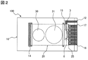
- FIG. 2 shows an example of a planar structure of the thermally-assisted magnetic recording head assembly 100 according to Embodiment 1 as viewed from the slider 20 side.
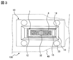
- FIG. 3 shows an example of a planar structure of the thermally-assisted magnetic recording head assembly 100 according to Embodiment 1 as viewed from the flexure 40 side.
- the semiconductor laser 1 is mounted on the thin film solder 11 in the recess 13 formed in the submount 10. At this time, the semiconductor laser 1 is positioned with reference to the alignment mark 6 formed on the semiconductor laser 1 and the alignment mark 18 formed on the submount 10.
- the thin film solder 11 formed on the flat portion (bottom surface portion) of the recess 13 of the submount 10 is preferably Au—Sn solder from the viewpoint of heat dissipation and position stability, and the temperature applied at that time is 300 ° C. or higher. Is common.
- the p-type electrode 5 of the semiconductor laser 1 is provided on the solder connection side with the submount 10 and the n-type electrode 4 is provided on the flexure 40 side. In general, a positive potential is applied to the lead line connected to the p-type electrode 5, and a negative potential is applied to the lead line connected to the n-type electrode 4.
- two types of adhesives 30 are used using a dispenser or the like in a region sandwiched between studs 14 on the side opposite to the mounting surface of the semiconductor laser 1 (the side of the submount 10 where the recess 13 is not formed). , 31 is applied. Thereafter, the alignment mark 6 of the semiconductor laser 1 that can be observed from the through hole 15 formed in the submount 10 and the alignment mark (not shown) formed on the slider 20 are aligned with each other, and the slider 20 is aligned with the submount 10. Is installed.
- the first adhesive 30 disposed on the inflow side of the slider 20 it is desirable to use a conductive adhesive that is cured by heat or a conductive adhesive that is given UV curing in addition to thermal curing.
- the second adhesive 31 disposed on the outflow side of the slider 20 it is desirable to use an adhesive that does not contain a filler and can be cured with both UV and heat characteristics.
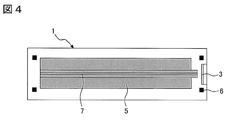
- FIG. 4 is a plan view of the semiconductor laser 1 as viewed from the p-type electrode 5 side (side of solder connection with the submount 10).
- alignment in the direction perpendicular to the resonance direction may be performed using an alignment mark 6 formed by a process for forming the mesa portion 7.
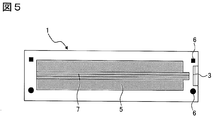
- the alignment mark 6 is desirably changed in shape with respect to the direction perpendicular to the resonator.
- the shape of the alignment mark 6 can be various patterns and sizes such as a circle, a quadrangle, and a rhombus, but it is desirable that the center be constant even if it varies.
- the edge of the semiconductor laser 1 is image-recognized in consideration of the configuration of the p-type electrode 5 of the semiconductor laser 1 and the thickness of the thin film solder 11 and the angle of the reflection mirror 3. The best way is to shift the correction amount later.
- alignment in the width direction may be performed using an alignment mark (not shown) formed simultaneously with the process of forming the core 23.
- the longitudinal direction of the slider with waveguide 20 it is necessary to apply an offset after recognizing an alignment mark (not shown) according to the thickness of the core 23.
- the first adhesive 30 and the second adhesive 31 are cured by UV and heat.
- the stud 14 formed on the submount 10 suppresses the extreme inclination of the semiconductor laser 1, prevents the adhesives 30 and 31 from flowing out to an excessive portion, traps outgas, and applies the adhesives 30 and 31. Used for range recognition, etc.
- the solder balls 17 are arranged on the submount 10, and the wirings are connected by melting by a laser.
- the molten solder is landed on the target region to connect the wirings.
- Sn-3Ag-0.5Cu is generally used as the solder.
- the solder locally becomes 250 ° C. or higher.
- a high-temperature load is also applied to the first adhesive 30 and the second adhesive 31 that have already been cured at the time of connection by solder.
- the second adhesive 31 disposed on the solder connection side is subjected to a higher temperature load than the first adhesive 30.
- the Young's modulus and hardness due to high temperature appears remarkably.
- the Young's modulus and hardness of the adhesive are significantly reduced, the force generated when the solder is solidified causes the mounting position of the core 23 formed on the slider 20 to shift. Therefore, the Young's modulus of the first adhesive 30 is set higher than that of the second adhesive 31.
- the first adhesive 30 can suppress misalignment associated with a decrease in Young's modulus of the second adhesive 31.
- the thermal conductivity of the second adhesive 31 is made smaller than that of the first adhesive 30, heat conduction to the first adhesive 30 can also be suppressed. It becomes possible to further suppress the decrease in Young's modulus of the first adhesive 30.
- the flexure 40 and the n-type electrode 4 (that is, the submount 10) of the semiconductor laser 1 are fixed with the conductive adhesive 32, and the submount 10 and the flexure 40 are fixed with the UV adhesive 33.
- the adhesive is cured by UV and heat as before. Since the conductive adhesive 32 is short-circuited when adhering to the active layer 2 of the semiconductor laser 1, it is better to provide the conductive adhesive 32 to some extent.
- the thickness of the n-type electrode 4 and the flexure 40 of the semiconductor laser 1 is better.
- the adhesive 33 for bonding the submount 10 and the flexure 40 be as thin as possible by providing a stud (not shown) on the flexure 40.
- solder connection method is the same as the method used to connect the wirings 16 and 25 of the submount 10 and the slider 20.
- the heat-assisted magnetic head assembly 100 is manufactured by the above assembly procedure.
- optical coupling and levitation characteristics are particularly important in order to satisfy the required performance.
- the distance between the semiconductor laser LD and the core 23 of the waveguide slider 20 is small, the peak portion of the intensity distribution of the laser light of the semiconductor laser 1 and the core in the waveguide slider 20. It is essential that the amount of displacement at the center of 23 is small.
- the thickness of the flat portion (bottom surface portion) of the recess 13 formed in the submount 10 is desirably 20 ⁇ m or less.
- misalignment when mounting the slider 20 on the adhesives 30 and 31 or when the adhesives 30 and 31 are cured becomes a problem.
- the adhesive 31 applied to the submount 10 in addition to the alignment mark 6 of the semiconductor laser 1 and the alignment mark (not shown) of the slider 20. , 31 is important. If an adhesive intervenes between the stud 14 and the slider 20 at the time of mounting, a slip phenomenon occurs when an external force is applied to the slider 20. For this reason, it is essential that no adhesive is sandwiched between the stud 14 and the slider 20.
- the conductive adhesive that is the first adhesive 30 contains a large amount of metal particles such as silver. For this reason, when the conductive adhesive which is the first adhesive 30 intervenes between the stud 14 and the slider 20, it causes a large displacement. For this reason, it is essential to control the bonding area particularly with respect to the first adhesive 30.
- the conductive adhesive tends to increase in viscosity, and when the viscosity is high, the adhesive thickness tends to increase.
- the increase in the adhesion thickness causes a decrease in optical coupling efficiency due to an increase in the distance between the semiconductor laser 1 and the core 23 of the slider 20.
- the maximum filler size of the conductive adhesive contained in the first adhesive 30 is smaller than the thickness of the stud 14 and that the second adhesive 31 does not contain a filler.
- the slider 20 is increasingly miniaturized, the current femto slider is the thinnest at 230 ⁇ m, and the flying height is as small as about 10 nm. For this reason, if the warpage of the order of several nanometers occurs unevenly, the flying characteristics deteriorate. Therefore, in order to ensure good flying characteristics, it is essential that the amount of deformation of the slider 20 is small.
- the semiconductor laser 1 is disposed in the vicinity of the slider 10 in order to give priority to optical coupling.
- the deformation of the slider 10 is accompanied by the deformation of the slider 10 due to the nonuniformity of the heat distribution, in addition to the deformation caused by the adhesive curing and the environmental change. For this reason, it is essential to secure a heat radiation path to the slider 10 that is not required in the conventional magnetic head unit.
- the thermal conductivity of an adhesive composed of acrylic and epoxy is about 0.2 W / mk, and a high thermal conductive adhesive of several W / mk or more contains many metal particles such as silver. Therefore, the Young's modulus tends to be high.
- the first adhesive 30 for heat dissipation has a Young's modulus at room temperature of 300 MPa or less, a Shore A hardness of 90 or less, and a thermal conductivity of at least 2 W / mK or more. It is desirable to use a thing, and it is good to make it smaller than that of the 2nd adhesive agent 31 as an adhesion area.
- the first adhesive 30 and the second adhesive 31 need to be bonded only to the surface opposite to the air bearing surface (ABS) of the slider 20.
- ABS air bearing surface
- the 1st adhesive agent 30 and the 2nd adhesive agent 31 mix, since the physical-property fall and intensity
- FIG. 6 shows a planar structure example when the thermally-assisted magnetic recording head assembly 100 according to the second embodiment is viewed from the slider 20 side.
- the first adhesive 30 is applied a plurality of times (in the case of the figure, twice).
- the apparent length of the first adhesive 30 with respect to the short (width) direction of the slider 20 is greatly changed.
- an adhesive with a dispenser or the like it is applied from a direction perpendicular to the submount 10 from the viewpoint of control. Therefore, the shape of the adhesive after application and mounting is a shape close to a circle.
- a change in the longitudinal direction adversely affects the flying characteristics as compared to the short direction.
- the first adhesive 30 by applying the first adhesive 30 a plurality of times to form a shape that is long in the lateral direction, it is possible to suppress a change in the longitudinal direction and to further ensure heat dissipation.
- FIG. 7 shows a planar structure example of the thermally-assisted magnetic recording head assembly 100 according to the third embodiment as viewed from the slider 20 side.
- a structure in which the periphery of the second adhesive 31 is surrounded by the stud 14 is employed.
- the stud 14 is formed first.
- FIG. 8 shows an example of a cross-sectional structure of the thermally-assisted magnetic recording head assembly 100 in this embodiment.
- FIG. 9 shows an example of a planar structure of the thermally-assisted magnetic recording head assembly 100 according to the fourth embodiment as viewed from the slider 20 side.
- a structure is adopted in which fillets are formed by a heat dissipating material 34 having high thermal conductivity through the submount 10 at both ends extending in the longitudinal direction of the slider 20.
- the first adhesive 30 has a higher thermal conductivity.
- an adhesive having high thermal conductivity has a high Young's modulus, it is difficult to bond a large area from the viewpoint of warpage.
- a heat dissipation path can be secured by disposing the heat dissipation material 34 on both ends of the slider 20 via the submount 10.
- the heat dissipation material 34 it is not necessary to consider the adhesive thickness, and the viscosity may be somewhat high. For this reason, it is also possible to contain Al 2 O 3 or SiO 2 filler having a large pulverized size that easily forms a heat dissipation path.
- the heat dissipation material 34 is not a type that exhibits a large adhesive strength such as an acrylic type or an epoxy type, but is a moisture-curing type resin that is cured by reacting with moisture in the air and has a silyl group that does not have a large adhesive force. It is good to use things. However, such a moisture curable resin contains an alcohol component and may flow out at the time of application, so that the stud is not attached to the submount 10 so as not to adhere to the first adhesive 30 or the second adhesive 31. It is desirable to provide 14.
- the heat radiating material 34 needs to contain as little as possible the material that is supposed to adhere to the magnetic disk 61, such as organic Sn or low-molecular siloxane.
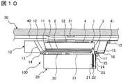
- FIG. 10 shows a cross-sectional structure example of the heat-assisted magnetic recording head assembly 100 according to the fifth embodiment.
- a structure in which the space between the surface from which the light of the semiconductor laser 1 exits and the core 23 of the slider 20 is filled with the second adhesive 31 is employed.
- the distance between the semiconductor laser 1 and the core 23 of the slider 20 is a small distance of several tens of ⁇ m, and the light of the semiconductor laser 1 is incident in a state of being wider than the core diameter of the slider 20.
- only a certain portion of the laser beam can be used for optical coupling, and a slight decrease in optical coupling efficiency is observed.
- the space is filled with a transparent material having a higher refractive index than air, the spread of the emitted light from the semiconductor laser 1 can be suppressed, and the effective distance until the same spot size is reduced. be able to. Further, by filling a material having a refractive index larger than that of air, reflection from the core 23 can be suppressed. For reducing the reflectance, an antireflection film may be formed on the light incident surface with respect to the core 23.
- the refractive index of the transparent second adhesive 31 to be filled is desirably 1.5 or more, and it is desirable to use a material having a transmittance of 98% or more with respect to the incident laser wavelength and good light resistance.
- the second adhesive 31 it is desirable to use an adhesive having excellent light resistance as the second adhesive 31.
- the second adhesive 30 is applied. Sometimes it becomes difficult to fill the coated part, so it becomes easier to fill.
- the adhesive filled between the semiconductor laser 1 and the core 23 of the waveguide-equipped slider 20 is the second adhesive 31
- a third adhesive 35 different from the second adhesive 31 may be filled.
- the second adhesive 31 is required to have a low viscosity. For this reason, if it is applied to the surface portion of the reflecting mirror 3 before the slider 20 is mounted, there is a possibility that it cannot be filled. In that case, a third adhesive 35 having a higher viscosity than the second adhesive 31 may be filled in between. Note that it is desirable to use an adhesive that does not contain a filler or contains a filler that is sufficiently smaller than the wavelength of the incident laser.
- FIG. 12 shows a planar structure example when the thermally-assisted magnetic recording head assembly 100 according to the sixth embodiment is viewed from the flexure 40 side.
- a structure in which a part of the periphery of the active layer 2 of the semiconductor laser 1 is sealed with a resin 36 is employed.
- the n-type electrode 4 of the semiconductor laser 1 is formed on the opposite surface to the p-type electrode 5, the n-type electrode 4 needs to be electrically connected to the flexure 40 through the conductive adhesive 32.
- the width of the semiconductor laser 1 is as narrow as about 200 ⁇ m.
- the conductive adhesive 32 protrudes to the active layer 2 of the semiconductor laser 1, and if a part of the conductive adhesive 32 is touched, a short circuit is caused. Therefore, in this embodiment, the portion of the active layer 2 of the semiconductor laser 1 in the vicinity where the conductive adhesive 32 is applied is surrounded by the resin 36.
- the resin 36 it is preferable to use a highly insulating adhesive or thermoplastic resin using UV for workability, and it is also preferable to use a resin having a low Young's modulus.
- the resin 36 is enclosed in the resonance direction of the semiconductor laser 1, the reflection characteristics change, so that it is necessary to design according to the refractive index of the resin 36.
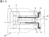
- FIG. 13 shows an example of a planar structure when the thermally-assisted magnetic recording head assembly 100 according to the seventh embodiment is viewed from the flexure 40 side.
- the p-type electrode 5 and the n-type electrode 4 of the semiconductor laser 1 are arranged on the same surface, and the semiconductor laser 1 is mounted on the thin film solder 11 portion of the recess 13 formed in the submount 10. is there.
- the possibility of a short circuit due to the conductive adhesive 32 can be greatly reduced.
- FIG. 14 shows an example of a cross-sectional structure of the heat-assisted magnetic recording head assembly 100 according to the eighth embodiment.
- the distance between the air bearing surface (ABS) and the magnetic disk 61 is about 10 nm.
- ABS air bearing surface
- the semiconductor laser 1 is made smaller by using cleavage, but there is a concern that the debris remains attached in the vicinity of the semiconductor laser 1 and peels off during levitation. .
- the resin 37 As the resin 37, the resin 36 described in the sixth embodiment may be used.
- the structure according to this embodiment is not limited to the case where the semiconductor laser 1 is a double-sided electrode, and is suitable for application to any of the structures described above.
- FIG. 15 is a diagram showing a schematic structural example of a magnetic disk drive device 200 on which the above-described heat-assisted magnetic recording head assembly 100 is mounted.
- a magnetic disk 61 as a recording medium is disposed in a housing 60 of the hard disk drive device 200, and the disk 61 is rotated at high speed by a spindle motor 62.
- a heat-assisted magnetic recording head assembly 100 according to the embodiment is mounted on one end of the suspension 50, and the other end is connected to the arm 63.
- the arm 63 is driven by a voice coil motor 64 to move the heat-assisted magnetic recording head assembly 100 to a recording position of the magnetic disk 61 that is rotationally driven.
- a signal processing LSI 65 for processing recording data writing and reading information is also arranged in the housing 60.
- Use of the present invention suppresses misalignment when mounting a slider with a waveguide on the submount and when curing the adhesive, and misalignment when soldering the slider with waveguide and the submount after curing the adhesive. can do. Thereby, good optical coupling between the submount and the slider with the waveguide can be realized. Further, the amount of warping of the slider during adhesive curing can be reduced. Furthermore, non-uniform deformation of the slider during semiconductor laser operation can be reduced by highly efficient heat radiation to the slider. Thereby, stable levitation characteristics can be satisfied. In addition, it can greatly contribute to extending the life of the semiconductor laser. With the above effects, a thermally assisted magnetic recording head assembly that satisfies both optical coupling and flying characteristics can be realized.
Landscapes
- Physics & Mathematics (AREA)
- Electromagnetism (AREA)
- Engineering & Computer Science (AREA)
- Manufacturing & Machinery (AREA)
- Recording Or Reproducing By Magnetic Means (AREA)
- Supporting Of Heads In Record-Carrier Devices (AREA)
- Adjustment Of The Magnetic Head Position Track Following On Tapes (AREA)
- Semiconductor Lasers (AREA)
- Magnetic Heads (AREA)
Abstract
磁気ヘッド部、光導波路及び近接場素子を有するスライダと、半導体レーザ、当該半導体レーザの共振方向の一端に配置され、レーザをその共振方向と交差する方向に反射させるミラーとを実装するサブマウントとを第1及び第2の接着剤で固定する。この際、第1及び第2の接着剤の少なくとも一部は、サブマウントを挟んで半導体レーザの対向位置に配置され、はんだ接続部を有するスライダの流出端側に設けた第2の接着剤に比べ、ヤング率の大きい第1の接着剤をスライダの流入端側に配置する。
Description
本発明は、近接場光により加熱した磁気記録媒体に磁界を印加して情報を記録する熱アシスト磁気記録ヘッドアセンブリの実装技術に関する。具体的には、熱アシスト磁気記録に対応する素子を搭載するスライダと半導体レーザを搭載するサブマウントとの接着構造に関する。また、当該接着構造を有する熱アシスト磁気ヘッドアセンブリを搭載する磁気ディスク装置に関する。
近年、磁気ディスク装置の記録密度を向上させる技術の一つとして、光記録と磁気記録を融合した光・磁気ハイブリッド記録技術が提案されている。この技術は、記録時に印加磁界の発生と同時に媒体を加熱し、媒体の保持力を低減させる手法を採用する。この手法の採用により、従来の磁気ヘッドでは記録磁界強度が不足して記録が困難であった高保持力の記録媒体にも、容易に記録できるようになる。一方、再生は、従来の磁気記録で用いられている磁気抵抗効果を使用する。
このハイブリッド記録方法を熱アシスト磁気記録と呼ぶ。ここで、光による加熱方法には、近接場を利用する方法が提案されている。近接場を用いた熱アシスト磁気記録では、レーザ光源が発生したレーザ光を記録ヘッドに導き、近接場光を発生させる機能を有する素子を用いて光スポット径を記録に適した大きさと形状に変換する。以下、このように近接場光を発生させる機能を有する素子のことを、近接場光発生素子という。
通常、レーザ光源には、ディスクドライブのパッケージ内で使用する必要性から、レーザ光源の中でも小型で低消費電力の半導体レーザ(LD:Laser Diode)が用いられる。Tb/in2 以上の記録密度を実現する近接場を用いた熱アシスト磁気記録装置で使用する用途では、記録媒体表面に達するまでに、数mW程度のパワーが必要となる。
半導体レーザで発生したレーザ光を近接場発生素子に導く光学部品は、反射ミラー、レンズ、光導波路などの光学部品である。半導体レーザから発生した光は、光路に配置された光学部品及び近接場発生素子を通過し、記録媒体へと到達する。レーザ光の光強度は、光路を通過する途中で減衰し、半導体レーザが発生した光出力の数十分の一になる。光強度が減衰する主な原因は、光学部品内を通過する時の吸収損失や散乱損失、光学部品の搭載や接着時及びはんだ付け時に生じる理想的な位置からのずれに起因する結合損失等である。従って、熱アシスト磁気記録においては、近接場発生素子に入射するまでの結合損失を小さくした構造が必須となる。
一方、磁気ディスクのスライダは小型化が進んでいる。例えば現在は、0.85mm× 0.7mm×0.23mmサイズのフェムトスライダが主流になってきている。また、浮上面(ABS:Air Bearing Surface)とディスクとの距離は10nm程度まで小さくなってきている。今後はさらに小型化が進み、浮上量が小さくなることも予想される。しかしながら、更なる小型化の進展及び低浮上量になった場合、スライダ自身の反りが大きな問題になると予測される。また、レーザ光の損失を小さくするためには、スライダ近傍への半導体レーザの配置が有効である。しかし、半導体レーザ自体が熱源となるため、スライダへの均一な放熱ができない場合、熱によるスライダの変形が加速されると共に、半導体レーザの寿命劣化が起きることが分かっている。そのため、スライダへの高効率な放熱構造が必須となる。このように、熱アシスト磁気記録ヘッドの実現には、位置ずれの低減による結合損失を小さくした構造に加え、スライダの反りを抑制しながらスライダに高効率で放熱可能な実装構造が必須となると予想される。
なお、特許文献1には、スライダとフレクチャの固定に、熱硬化接着剤とUV接着剤を使うことで取り付け寸法のばらつきを小さくし、精度向上を図った固定方法が開示されている。また、特許文献2には、スライダとフレクチャの接合部に、光硬化と熱硬化の両性質を有する接着剤を介在させ、接着剤の塗布領域以外に熱硬化接着剤及び電気的に導通させるための導電性接着剤を介在させることでスライダとフレクチャの接着強度を向上させた磁気ヘッドが示されている。また、特許文献3には、スライダと接着する光源支持基板の接着面の少なくとも一部に凹面を形成することにより、光源の位置を精度良く調整可能にした熱アシスト磁気ヘッドが示されている。
ところで、特許文献1は、ロードビームの影になるために紫外線照射が困難な箇所に熱硬化型接着剤を使用する一方で、紫外線照射が可能な箇所にはUV接着剤を使用することによるフレクチャとスライダの固定技術を開示する。ところが、この特許文献1に開示される構造は、従来型の磁気ヘッドのフレクチャとスライダの接着構造に関するものであり、熱源となり得る半導体レーザがそもそも実装されていない。このため、スライダへの放熱が考慮されていない。また、2種類の接着剤の使用目的は接着強度の向上である。このため、2種類の接着剤の物性値差、位置ずれ抑制、はんだ付け部分に対する接着剤の位置関係についての考察は記載されていない。
特許文献2は、フレクチャとスライダの間に3種類の接着剤を使用し、フレクチャとスライダを固定する。しかし、特許文献2も、従来型の磁気ヘッドを想定するため、光結合のために必要な光導波路は形成されておらず、ゆえにスライダの長手方向の全面を接着している。このため、特許文献2に開示された構造は、熱アシスト磁気ヘッドに適用することはできない。また、3種類の接着剤に境界を設けていないため、接着剤同士が混ざり合った結果、十分な硬化特性を満たせず、接着強度低下や所望の物性を得られなくなることもしばしば起こる。さらに、3種類の接着剤を用いる目的も、特許文献1と同様の接着強度と静電破壊の防止である。このため、スライダへの放熱については、やはり考慮されていない。その上、特許文献1の場合と同様に、3種類の接着剤の物性値差、位置ずれ抑制、はんだ付け部分に対する接着剤の位置関係についても記載されていない。
特許文献3は、半導体レーザを実装した光源支持板のスライダとの接着面に凹部を形成し、この凹部によって接着剤の流出を抑制する。しかし、凹部に対して1種類の接着剤を配置しただけでは、放熱性や位置ずれ抑制について課題が多い。
そこで、本発明では、スライダへの放熱性と浮上特性を確保しつつ、半導体レーザからの光を効率良く、スライダに形成した導波路に伝播させることで、高密度対応を可能とした熱アシスト磁気記録ヘッドアセンブリの構造を提案する。
具体的には、磁気ヘッド部、光導波路及び近接場素子を有するスライダ(熱アシスト磁気ヘッド及び導波路付きスライダ)と、半導体レーザと、当該半導体レーザの共振方向の一端に配置され、レーザをその共振方向と交差する方向に反射させるミラーとを実装するサブマウントとの接続構造を提案する。なお、この接続構造において、スライダとサブマウントを取り付け面において固定する第1及び第2の接着剤の少なくとも一部は、サブマウントを挟んで半導体レーザの対向位置に配置されるものとする。また、はんだ接続部を有するスライダの流出端側(エアの流出側)に設けた第2の接着剤に比べ、ヤング率の大きい第1の接着剤を、スライダの流入端側(エアの流入側)に配置するものとする。この接続構造により、スライダとサブマウントとの位置ずれを抑制して良好な光結合を実現することができる。また、接着剤の少なくとも一部が半導体レーザの対向位置に配置されるので、半導体レーザの熱を高効率にスライダ側に逃がすことができる。
なお、以上の接続構造において、第1の接着剤の熱伝導率は第2の接着剤に比べて大きいことが望ましい。この構造の採用により、はんだ接続時における第1の接着剤への熱伝導を抑制することができ、第1の接着剤の変形を抑制することができる。これにより、スライダの反りが更に抑制され、良好な浮上特性を実現することができる。
また、以上の接続構造において、第1及び第2の接着剤の厚みは、スライダとサブマウント間の距離と同一になるように設定し、第1及び第2の接着剤がスライダ端部からはみ出さないことが望ましい。この構造の採用により、スライダの反りの要因であるフィレットの形成をなくすことができる。
また、以上の接続構造において、半導体レーザは、その全体がサブマウントに形成された凹部に収容されるように実装されることが望ましい。この構造の採用により、導電性接着剤の半導体レーザの活性層面への付着を抑制し、ショート防止が可能となる。
また、以上の接続構造において、半導体レーザのアライメントマークをメサ部に対して対称に少なくとも2つ形成し、かつ、対称に位置する少なくとも2つのアライメントマークの形状が異なっていることが望ましい。この構造の採用により、アライメント精度を向上することができる。
また、以上の接続構造において、第1の接着剤におけるフィラーの最大サイズをサブマウントに形成したスタッド高さよりも小さくすることが望ましい。この構造の採用により、接着剤の薄膜化やスライダ搭載時のずれの抑制を実現できる。
また、以上の接続構造において、導波路と半導体レーザ面の間の光が通過する部分を、透明な第2の接着剤又は透明な第3の接着剤で充填することが望ましい。この構造の採用により、レーザ光の同一のスポットサイズになるまでの実効的な距離を小さくできる。
また、以上の接続構造において、半導体レーザの活性層の周りの一部を、第1及び第2の接着剤又は熱可塑性樹脂で囲うことが望ましい。この構造の採用により、電極間の短絡を効果的に抑制できる。
また、以上の接続構造において、半導体レーザの端部分の一部又は全面を、接着剤又は熱可塑性樹脂にて囲うことが望ましい。この構造の採用により、半導体レーザやサブマウントに付着した半導体の屑の飛散を効果的に抑制できる。
また、以上の接続構造において、スライダとサブマウントの端部分の少なくとも一部に、放熱材を用いてフィレットを形成することが望ましい。この構造の採用により、放熱効率を更に高めることができる。なお、放熱材の弾性率又は硬度を、第1及び第2の接着剤に比べて小さくすることが望ましい。
また、以上の接続構造において、第2の接着剤の外周部を、サブマウントに形成したスタッドにて囲むことが望ましい。この構造の採用により、第2の接着剤の余分な部分へのはみ出しを防止することができる。
また、以上の接続構造においては、第1の接着剤の接着面積に比べ、第2の接着剤の接着面積を大きくすることが望ましい。この構造の採用により、第1の接着剤による反りを抑制した上で、放熱も可能となる。
本発明によれば、スライダとサブマウントとの位置ずれを抑制して良好な光結合を実現することができる。また、接着剤の少なくとも一部が半導体レーザの対向位置に配置されるので、半導体レーザの熱を高効率にスライダ側に逃がすことができる。これにより、半導体レーザの動作中におけるスライダの不均一な変形を低減できる。この結果、良好な浮上特性を満足できると共に、半導体レーザの長寿命化を実現できる。以上により、高密度記録に対応した熱アシスト磁気記録ヘッドアセンブリを実現することができる。
1・・・半導体レーザ、2・・・活性層、3・・・反射ミラー、4・・・半導体レーザのn型電極、5・・・半導体レーザのp型電極、6・・・半導体レーザのアライメントマーク、7・・・メサ部、10・・・サブマウント、11・・・薄膜はんだ、12・・・半導体レーザのp型電極との接続用電極、13・・・サブマウントの凹部、14・・・スタッド、15・・・貫通孔、16・・・スライダとの接続用電極、17・・・はんだボール、18・・・サブマウントのアライメントマーク、20・・・スライダ、21・・・磁気記録・検出素子、22・・・近接場発生素子、23・・・光導波路のコア、24・・・光導波路のクラッド、25・・・スライダの電極、30・・・第1の接着剤、31・・・第2の接着剤、32・・・導電性接着剤、33・・・第3の接着剤、34・・・放熱材、35・・・接着剤、36・・・樹脂、37・・・樹脂、40・・・フレクチャ、41・・・電極、50・・・サスペンション、51・・・ディンプル、60・・・筐体、61・・・磁気ディスク、62・・・スピンドルモータ、63・・・アーム、64・・・ボイスコイルモータ、65・・・信号処理用LSI、66・・・ランプ、100・・・熱アシスト磁気ヘッドアセンブリ、200・・・磁気ディスク駆動装置
以下、図面に基づいて、本発明の実施例を説明する。なお、後述する装置構成や処理動作の内容は発明を説明するための一例であり、本発明は、後述する装置構成や処理動作に既知の技術を組み合わせた発明や後述する装置構成や処理動作の一部を既知の技術と置換した発明も包含する。
以下、熱アシスト磁気記録ヘッドアセンブリの接続構造例を、図面を用いて説明する。熱アシスト磁気記録ヘッドアセンブリの主要部品は、スライダ、半導体レーザ、サブマウントである。ここで、スライダを構成する主要な素子は、光導波路と、近接場発生素子と、磁界記録・検出素子(磁気ヘッド部)である。一方、サブマウントは、端面近傍に反射ミラーを形成した半導体レーザを実装する。半導体レーザは動作中に高温になるが、その時の温度と発光特性や寿命との間には密接な関係がある。従って、放熱性を確保するために、半導体レーザとそれを実装するサブマウントとの接続は、活性層を接続面に近い位置に配置するジャンクションダウン構造をとることが望ましい。また、半導体レーザとサブマウントとは、光を伝搬させる光導波路との相対位置が経時変化することを避けるために、クリープ変形の極めて小さい Au-Snはんだを用いるのが好ましい。また、良好な放熱を確保できない場合に、半導体レーザの寿命が低下する以外に、動作によりスライダの反りが発生するという問題がある。この反りの程度が大きくなると浮上特性が悪化する。そのため、半導体レーザの熱をスライダに効率良く逃がすことが必須となる。従って、基板の材料としては、熱伝導率の高いもの、半導体レーザの基板材質(GaAs)やスライダ材質(AlTiC)のそれに近い熱膨張係数を有する材質を用いるのが望ましい。具体的には、SiC、Al2O3、AlN、Si、AlTiCなどから、加工性などを加味して選ぶと良い。基板の厚みとしては、浮上特性、剛性などから80μm~150μm程度が好ましい。
スライダの一端面には、光導波路が、スライダの厚さ方向にスライダの上面から下面に貫通するように設けられている。さらに、スライダの浮上面(ABS:Air Bearing Surface)には、近接場発生素子や磁気記録・検出素子(磁気ヘッド部)が設けられている。スライダの材料としては、AlTiCが従来から使用されている。以上の構成する材質を接着剤やはんだなどの接続部材を用いて高精度に固定することが重要となる。
(1)形態例1
図1に、形態例1に係る熱アシスト磁気記録ヘッドアセンブリ100の断面構造例を示す。図1に示すように、熱アシスト磁気記録ヘッドアセンブリ100は、サブマウント10と、スライダ20と、これらを固定する2種類の接着剤30、31とで構成される。サブマウント10には、スライダ20側に形成される光導波路と対面するように貫通孔15が形成されており、この貫通孔15にレーザ光を導くように反射ミラー3を形成した半導体レーザ1が実装されている。すなわち、反射ミラー3は半導体レーザ1の端面付近に形成される。スライダ20には、光導波路(コア23、クラッド24)と、近接場発生素子22と、磁気記録・検出素子21とが実装される。サブマウント10とスライダ20を固定する2種類の接着剤30、31の少なくとも一部は、サブマウント10を挟んで半導体レーザ1の下部に位置するように配置される。この際、はんだ接続部が形成されるスライダ20の流出端側に配置される第2の接着剤31に比べ、ヤング率の大きい第1の接着剤30がスライダ20の流入側に配置される。
図1に、形態例1に係る熱アシスト磁気記録ヘッドアセンブリ100の断面構造例を示す。図1に示すように、熱アシスト磁気記録ヘッドアセンブリ100は、サブマウント10と、スライダ20と、これらを固定する2種類の接着剤30、31とで構成される。サブマウント10には、スライダ20側に形成される光導波路と対面するように貫通孔15が形成されており、この貫通孔15にレーザ光を導くように反射ミラー3を形成した半導体レーザ1が実装されている。すなわち、反射ミラー3は半導体レーザ1の端面付近に形成される。スライダ20には、光導波路(コア23、クラッド24)と、近接場発生素子22と、磁気記録・検出素子21とが実装される。サブマウント10とスライダ20を固定する2種類の接着剤30、31の少なくとも一部は、サブマウント10を挟んで半導体レーザ1の下部に位置するように配置される。この際、はんだ接続部が形成されるスライダ20の流出端側に配置される第2の接着剤31に比べ、ヤング率の大きい第1の接着剤30がスライダ20の流入側に配置される。
図2に、形態例1に係る熱アシスト磁気記録ヘッドアセンブリ100をスライダ20側から見た平面構造例を示す。図3に、形態例1に係る熱アシスト磁気記録ヘッドアセンブリ100をフレクチャ40側から見た平面構造例を示す。
ここでは、図1~図3を用い、形態例1に係る熱アシスト磁気記録ヘッドアセンブリ100の組み立て手順を説明する。まず、半導体レーザ1をサブマウント10に形成された凹部13の薄膜はんだ11上に搭載する。この際、半導体レーザ1に形成されたアライメントマーク6とサブマウント10に形成されたアライメントマーク18を基準に、半導体レーザ1の位置決めが行われる。
この後、リフローし、半導体レーザ1とサブマウント10とを接続する。なお、サブマウント10の凹部13の平坦部(底面部)に形成された薄膜はんだ11は、放熱性や位置安定性の観点から Au-Snはんだを用いると良く、その時に加える温度は 300℃以上が一般的である。また、この形態例の場合、半導体レーザ1のp型電極5は、サブマウント10とのはんだ接続側に、n型電極4はフレクチャ40側に設けている。なお、p型電極5に接続されているリードラインに正電位を加え、n型電極4に接続されているリードラインに負電位を加えるのが一般的である。
次に、半導体レーザ1の実装面とは逆面側(サブマウント10のうち凹部13が形成されていない側)のスタッド14で挟まれる領域内に、ディスペンサー等を用いて2種類の接着剤30、31を塗布する。この後、サブマウント10に形成された貫通孔15から観察可能な半導体レーザ1のアライメントマーク6とスライダ20に形成したアライメントマーク(図示せず)を基準に位置合わせし、サブマウント10にスライダ20を搭載する。
ここで、スライダ20の流入側に配置される第1の接着剤30には、熱で硬化する導電性接着剤又は熱硬化に加えUV硬化を付与した導電性接着剤を用いることが望ましい。一方、スライダ20の流出側に配置される第2の接着剤31には、フィラーを含まないUVと熱の両方の特性で硬化可能な接着剤が用いることが望ましい。
また、半導体レーザ1側のアライメントマーク6と導波路付きスライダ20側のアライメントマーク(図示せず)の精度は、光結合に大きく影響する。このため、2つのアライメントマークの精度は非常に重要である。図4に、半導体レーザ1のp型電極5側(サブマウント10とのはんだ接続側)から見た平面図を示す。
半導体レーザの場合、共振方向に対する垂直面方向の位置合わせは、メサ部7を形成する時のプロセスで形成したアライメントマーク6を用いると良い。なお、アライメントマーク6は、図5に示すように、共振器と垂直面方向に対して形状を変えることが望ましい。アライメントマーク6の形状は、円形、四角形、ひし形など様々なパターンやサイズが可能であるが、ばらついたとしても中心が一定になるようにできる形状が望ましい。
ところで、反射ミラー3を集積した半導体レーザ1では、端面から光が反射されて出力される。このため、半導体レーザ1の共振方向の位置合わせは、半導体レーザ1のp型電極5の構成や薄膜はんだ11の厚みと反射ミラー3の角度を考慮して、半導体レーザ1のエッジを画像認識した後に補正分ずらして搭載する方法が最も良い。
一方、導波路付きスライダ20の場合、幅方向の位置合わせは、コア23を形成するプロセスで同時に形成したアライメントマーク(図示せず)を使用すると良い。導波路付きスライダ20の長手方向に関しては、コア23の積層厚に応じて、アライメントマーク(図示せず)を画像認識した後で、オフセットをかける必要がある。前述したプロセスを用いてサブマウント10にスライダ20を搭載した後に、UV及び熱によって第1の接着剤30と第2の接着剤31とを硬化させる。ここで、サブマウント10に形成されるスタッド14は、半導体レーザ1の極端な傾きの抑制、接着剤30、31の余分な部分への流出防止、アウトガスのトラップ、接着剤30、31を塗布する範囲の認識等のために用いられる。なお、磁気ヘッド部の耐熱性を考慮すると、できる限り 100℃程度の低温で硬化する接着剤を用いることが望ましい。また、接着剤30、31は、サブマウント10を挟んで半導体レーザ1のp型電極5の真下位置に配置すると、最も放熱性が良好な構造になる。
この後、サブマウント10と導波路付きスライダ20の配線12、16、25を接続するために、はんだボール17をサブマウント10に配置し、レーザによる溶融により配線同士を接続する。その他の方法として、溶融した状態のはんだを標的領域に着弾させて配線同士を接続する方法もある。この場合、はんだとしては Sn-3Ag-0.5Cuが一般的に使用される。このため、はんだは局所的に 250℃以上になる。このように、はんだによる接続時には、既に硬化している第1の接着剤30及び第2の接着剤31に対しても高温の負荷を与える。特に、はんだ接続側に配置される第2の接着剤31は、第1の接着剤30に比べてより高温の負荷が加えられる。このため、高温によるヤング率や硬度の低下は顕著に現れる。接着剤のヤング率や硬度の大幅な低下が起こると、はんだ凝固時に発生する力によって、スライダ20に形成されたコア23の取り付け位置をずらす要因となる。そこで、第2の接着剤31に比べて第1の接着剤30のヤング率を高くする。このことで、第2の接着剤31のヤング率低下に伴う位置ずれを第1の接着剤30で抑制することが可能となる。この際、ヤング率に加えて、第1の接着剤30に比べて、第2の接着剤31の熱伝導率を小さくしておけば、第1の接着剤30への熱伝導も抑制することが可能となり、第1の接着剤30のヤング率低下を一層抑えることが可能となる。
次に、フレクチャ40と半導体レーザ1のn型電極4(すなわち、サブマウント10)とを導電性接着剤32で固定すると共に、サブマウント10とフレクチャ40とをUV接着剤33を用いて固定する。なお、この際、UV接着剤33は、UVに加えて熱を併用した接着剤を、導電性接着剤32は、熱硬化に加えてUVも併用した接着剤を用いることが望ましい。その後、これまでと同様にUV及び熱によって接着剤を硬化させる。なお、導電性接着剤32が半導体レーザ1の活性層2に付着するとショートするため、ある程度、導電性接着剤32の厚みを設けた方が良く、半導体レーザ1のn型電極4とフレクチャ40の距離に比べ、サブマウント10のフレクチャ40との接続面とフレクチャ40との距離を大きくすることが望ましい。一方で、スライダ20とフレクチャ40が接着剤の厚い部分のみで固定されていると、浮上中に弾性変形が起き、浮上特性が安定しないことが懸念される。従って、サブマウント10とフレクチャ40とを接着する接着剤33は、フレクチャ40にスタッド(図示せず)を設けるなどして可能な限り接着厚を小さくすることが望ましい。
次に、フレクチャ40に形成された配線41とサブマウント10に形成された配線12、16をはんだで接続する。このはんだの接続方法は、サブマウント10とスライダ20の配線16、25を接続するのに用いた方法と同様である。
一般に、以上の組立て手順により、熱アシスト磁気ヘッドアセンブリ100を作製する。ただし、必要とされる性能を満足するためには、光結合及び浮上特性が特に重要となる。高効率な光結合を達成するためには、半導体レーザLDと導波路付きスライダ20のコア23の距離が小さいこと及び半導体レーザ1のレーザ光の強度分布のピーク部分と導波路付きスライダ20におけるコア23の中心部の位置ずれ量が小さいことが必須となる。
そのため、サブマウント10に形成された凹部13の平坦部(底面部)の厚みは20μm以下であることが望ましい。
また、位置ずれについては、前述したはんだ接続時の位置ずれ以外にも、接着剤30、31にスライダ20を搭載する時や接着剤30、31が硬化する時の位置ずれが課題となる。接着剤30、31にスライダ20を搭載する時の高精度化については、半導体レーザ1のアライメントマーク6とスライダ20のアライメントマーク(図示せず)に加えて、サブマウント10に塗布する接着剤31、31の面積や形状が重要となる。搭載時に、スタッド14とスライダ20の間に接着剤が介入すると、スライダ20に外力が加わった場合に滑り現象が生じる原因となる。このため、スタッド14とスライダ20の間には接着剤を挟まないことが必須となる。特に、第1の接着剤30である導電性接着剤は、銀などの金属粒子が多く入っている。このため、第1の接着剤30である導電性接着剤がスタッド14とスライダ20の間に介入した場合には大きな位置ずれが生じる原因になる。このため、特に第1の接着剤30に関しては接着面積を制御することが必須である。
さらに、導電性接着剤は粘度が高くなりやすく、粘度が高い場合、接着厚が厚くなる傾向にある。接着厚の増加は、半導体レーザ1とスライダ20のコア23との距離の増加による光結合効率の低下をもたらす。このため、2種類の接着剤30、31には、可能な限り粘度が低いものを用いると良い。特に、第1の接着剤30に含有する導電性接着剤の最大フィラーサイズは、スタッド14の厚みよりも小さくし、第2の接着剤31に関しては、フィラーを含まないものを用いることが望ましい。
現在のハードディスク装置において、スライダ20はますます小型化しており、現在フェムトスライダが230μmと最も薄く、浮上量は10nm程度と小さい。このため、数nmオーダの反りが不均一に起こると、浮上特性が悪化する。そこで、良好な浮上特性を確保するためには、スライダ20の変形量が小さいことが必須となる。形態例に係る熱アシスト磁気ヘッドアセンブリ100においては、光結合を優先させるために、スライダ10の近傍に半導体レーザ1を配置している。このため、スライダ10の変形原因には、これまでの接着硬化時や環境変化に起因した変形に加えて、熱分布の不均一性に伴うスライダ10の変形が加わる。このため、従来の磁気ヘッド部では求められていないスライダ10への放熱経路の確保が必須となる。
一般的に、熱抵抗を小さくするためには、熱伝導率大、接着厚小、接着面積大とする必要がある。このパラメータの中で、接着厚や接着面積をそれほど大きく変えることはできないが、熱伝導率に対してはオーダを変えられる程度まで調整が可能であり、効果的な放熱を行うのに有効なパラメータである。一般的にアクリル及びエポキシなどで構成される接着剤の熱伝導率は、 0.2W/mk程度であり、数W/mk以上の高熱伝導性の接着剤は、銀などの金属粒子を多く含有させるため、ヤング率が高くなる傾向にある。ヤング率が高い接着剤を用いて大面積で接着すると、接着硬化時、環境変化時(特に低温時)に大きな反りが発生するという問題がある。従って、放熱性の確保と硬化時及び環境変化時の反りを抑制するためには、形態例の場合のように2種類の接着剤を使うことが必須となる。
前述した2種類の接着剤30、31のうち、放熱を目的とした第1の接着剤30は、室温でのヤング率300MPa以下、ショアA硬度90以下、熱伝導率は少なくとも2W/mK以上のものを使用することが望ましく、また、接着面積として、第2の接着剤31のそれより小さくすると良い。
また、前述した第1の接着剤30及び第2の接着剤31によって、スライダ20の端部分にフィレットを形成した場合、反りが大幅に大きくなることは分かっている。そのため、第1の接着剤30及び第2の接着剤31は、スライダ20の浮上面( ABS)と反対面のみに接着する必要がある。なお、第1の接着剤30と第2の接着剤31とが混ざり合った場合、硬化不良に伴う物性低下及び強度低下が起こるため、互いに混ざり合わないように塗布することが必要である。
(2)形態例2
図6に、形態例2に係る熱アシスト磁気記録ヘッドアセンブリ100をスライダ20側から見た平面構造例を示す。この形態例の場合、第1の接着剤30を複数回(図の場合は2回)塗布する。これにより、スライダ20の短手(幅)方向に対する第1の接着剤30の見かけ上の長さを大きく変えている。通常、ディスペンサー等で接着剤を塗布する場合、制御の観点からサブマウント10に対して垂直な方向から塗布する。そのため、塗布及び搭載後の接着剤の形状は、円形に近い形状となる。特に、スライダ20の変形は、短手方向に比べ長手方向の変化が浮上特性に対して悪影響を及ぼす。そこで、第1の接着剤30を複数回塗布し、短手方向に長い形状とすることで、長手方向の変化を抑制し、かつ、より一層の放熱性の確保が可能となる。ただし、複数回塗布することは生産性の観点で好ましくないことから、第2の接着剤31に関しては1回の塗布が望ましい。
図6に、形態例2に係る熱アシスト磁気記録ヘッドアセンブリ100をスライダ20側から見た平面構造例を示す。この形態例の場合、第1の接着剤30を複数回(図の場合は2回)塗布する。これにより、スライダ20の短手(幅)方向に対する第1の接着剤30の見かけ上の長さを大きく変えている。通常、ディスペンサー等で接着剤を塗布する場合、制御の観点からサブマウント10に対して垂直な方向から塗布する。そのため、塗布及び搭載後の接着剤の形状は、円形に近い形状となる。特に、スライダ20の変形は、短手方向に比べ長手方向の変化が浮上特性に対して悪影響を及ぼす。そこで、第1の接着剤30を複数回塗布し、短手方向に長い形状とすることで、長手方向の変化を抑制し、かつ、より一層の放熱性の確保が可能となる。ただし、複数回塗布することは生産性の観点で好ましくないことから、第2の接着剤31に関しては1回の塗布が望ましい。
(3)形態例3
図7に、形態例3に係る熱アシスト磁気記録ヘッドアセンブリ100をスライダ20側から見た平面構造例を示す。この形態例では、第2の接着剤31の周囲をスタッド14で囲んだ構造を採用する。勿論、スタッド14が先に形成されている。図8に、この形態例における熱アシスト磁気記録ヘッドアセンブリ100の断面構造例を示す。第2の接着剤31にフィラーを含有しない接着剤を用いると、厚みを薄くでき、しかも、ヤング率を小さくすることができる。しかし、その分、粘度が低くなりすぎる場合がある。このような場合、第2の接着剤31の周りにスタッド14を配置しておけば、塗布時に第2の接着剤31が塗れ広がったとしてもスライダ20の外に接着剤がはみだすことがなく、面積もある程度制御することができる。
図7に、形態例3に係る熱アシスト磁気記録ヘッドアセンブリ100をスライダ20側から見た平面構造例を示す。この形態例では、第2の接着剤31の周囲をスタッド14で囲んだ構造を採用する。勿論、スタッド14が先に形成されている。図8に、この形態例における熱アシスト磁気記録ヘッドアセンブリ100の断面構造例を示す。第2の接着剤31にフィラーを含有しない接着剤を用いると、厚みを薄くでき、しかも、ヤング率を小さくすることができる。しかし、その分、粘度が低くなりすぎる場合がある。このような場合、第2の接着剤31の周りにスタッド14を配置しておけば、塗布時に第2の接着剤31が塗れ広がったとしてもスライダ20の外に接着剤がはみだすことがなく、面積もある程度制御することができる。
(4)形態例4
図9に、形態例4に係る熱アシスト磁気記録ヘッドアセンブリ100をスライダ20側から見た平面構造例を示す。この形態例では、スライダ20の長手方向に延びる両端部にサブマウント10を介して熱伝導率の高い放熱材34でフィレットを形成する構造を採用する。これまで説明したように、第1の接着剤30の熱伝導率は高い方が好ましい。一方で、熱伝導率が高い接着剤はヤング率が高くなるので、反りの観点からは大面積での接着が困難である。そこで、前述した構造で放熱性の確保が難しい場合には、放熱材34をスライダ20の両端にサブマウント10を介して配置することで放熱経路を確保することができる。特に、放熱材34の場合は、接着厚を考慮する必要がなく、粘度が多少高くても良い。このため、放熱経路を形成し易い粉砕サイズの大きい Al2O3やSiO2フィラーを含有することも可能である。なお、放熱材34はアクリル系やエポキシ系などの大きな接着強度を発現するタイプではなく、空気中の水分で反応して硬化する湿気硬化型樹脂で大きな接着力を有さないシリル基含有のタイプのものなどを用いると良い。ただし、このような湿気硬化型の樹脂はアルコール成分を含んでおり、塗布時に流れ出すことがあるので、第1の接着剤30や第2の接着剤31に付着しないように、サブマウント10にスタッド14を設けておくことが望ましい。なお、放熱材34は、有機Snや低分子のシロキサンなど磁気ディスク61に付着するとされている材質を極力含まないことが必要である。
図9に、形態例4に係る熱アシスト磁気記録ヘッドアセンブリ100をスライダ20側から見た平面構造例を示す。この形態例では、スライダ20の長手方向に延びる両端部にサブマウント10を介して熱伝導率の高い放熱材34でフィレットを形成する構造を採用する。これまで説明したように、第1の接着剤30の熱伝導率は高い方が好ましい。一方で、熱伝導率が高い接着剤はヤング率が高くなるので、反りの観点からは大面積での接着が困難である。そこで、前述した構造で放熱性の確保が難しい場合には、放熱材34をスライダ20の両端にサブマウント10を介して配置することで放熱経路を確保することができる。特に、放熱材34の場合は、接着厚を考慮する必要がなく、粘度が多少高くても良い。このため、放熱経路を形成し易い粉砕サイズの大きい Al2O3やSiO2フィラーを含有することも可能である。なお、放熱材34はアクリル系やエポキシ系などの大きな接着強度を発現するタイプではなく、空気中の水分で反応して硬化する湿気硬化型樹脂で大きな接着力を有さないシリル基含有のタイプのものなどを用いると良い。ただし、このような湿気硬化型の樹脂はアルコール成分を含んでおり、塗布時に流れ出すことがあるので、第1の接着剤30や第2の接着剤31に付着しないように、サブマウント10にスタッド14を設けておくことが望ましい。なお、放熱材34は、有機Snや低分子のシロキサンなど磁気ディスク61に付着するとされている材質を極力含まないことが必要である。
(5)形態例5
図10に、形態例5に係る熱アシスト磁気記録ヘッドアセンブリ100の断面構造例を示す。この形態例では、半導体レーザ1の光が出てくる面とスライダ20のコア23との間を第2の接着剤31で充填する構造を採用する。前述した形態例の場合、半導体レーザ1とスライダ20のコア23との距離は数10μmと小さいながら距離があり、半導体レーザ1の光はスライダ20のコア径よりも広がった状態で入射される。その結果、レーザ光のある程度の部分しか光結合に使用することができず、若干の光結合効率の低下が認められる。そのため、透明かつ空気よりも屈折率の大きい材質をその空間に充填すれば、半導体レーザ1の出射光の広がりを抑制することができ、同一のスポットサイズになるまでの実効的な距離を小さくすることができる。また、空気よりも屈折率の大きい材質を充填することにより、コア23との反射も抑えることが可能となる。なお、反射率の低減に対しては、コア23に対する光の入射面に反射防止膜を形成しても良い。充填する透明な第2の接着剤31の屈折率は、 1.5以上であることが望ましく、入射するレーザ波長に対して透過率98%以上かつ耐光性の良いものを使用するのが望ましい。その上で、第2の接着剤31には、耐光性に優れた接着剤を用いることが望ましい。なお、この接続構造を採用する場合、スタッド14は、図10に示すように、貫通孔15とはんだ接続部との間に設けることが望ましい。さらに、貫通孔15の斜面や半導体レーザ1の実装面に達する傾斜面の部分に、Auその他の接着剤に比べ表面自由エネルギーの小さい材質をコーティングしておけば、第2の接着剤30の塗布時にもコーティング部分には塗ることができなくなるので充填しやすくなる。
図10に、形態例5に係る熱アシスト磁気記録ヘッドアセンブリ100の断面構造例を示す。この形態例では、半導体レーザ1の光が出てくる面とスライダ20のコア23との間を第2の接着剤31で充填する構造を採用する。前述した形態例の場合、半導体レーザ1とスライダ20のコア23との距離は数10μmと小さいながら距離があり、半導体レーザ1の光はスライダ20のコア径よりも広がった状態で入射される。その結果、レーザ光のある程度の部分しか光結合に使用することができず、若干の光結合効率の低下が認められる。そのため、透明かつ空気よりも屈折率の大きい材質をその空間に充填すれば、半導体レーザ1の出射光の広がりを抑制することができ、同一のスポットサイズになるまでの実効的な距離を小さくすることができる。また、空気よりも屈折率の大きい材質を充填することにより、コア23との反射も抑えることが可能となる。なお、反射率の低減に対しては、コア23に対する光の入射面に反射防止膜を形成しても良い。充填する透明な第2の接着剤31の屈折率は、 1.5以上であることが望ましく、入射するレーザ波長に対して透過率98%以上かつ耐光性の良いものを使用するのが望ましい。その上で、第2の接着剤31には、耐光性に優れた接着剤を用いることが望ましい。なお、この接続構造を採用する場合、スタッド14は、図10に示すように、貫通孔15とはんだ接続部との間に設けることが望ましい。さらに、貫通孔15の斜面や半導体レーザ1の実装面に達する傾斜面の部分に、Auその他の接着剤に比べ表面自由エネルギーの小さい材質をコーティングしておけば、第2の接着剤30の塗布時にもコーティング部分には塗ることができなくなるので充填しやすくなる。
なお、以上の説明では、半導体レーザ1と導波路付きスライダ20のコア23との間に充填する接着剤を第2の接着剤31とする場合について説明したが、図11に示すように、第2の接着剤31とは異なる第3の接着剤35で充填しても良い。前述したように、第2の接着剤31は粘度が低いことが求められる。このため、スライダ20を搭載する前に反射ミラー3の面部分に塗布しておいた場合、充填できない可能性もある。その場合は、第2の接着剤31よりも粘度が高い第3の接着剤35を間に充填すると良い。なお、充填する材料は、フィラーを含まない又は入射するレーザの波長に比べて十分に小さいフィラーを含む接着剤を使用することが望ましい。
(6)形態例6
図12に、形態例6に係る熱アシスト磁気記録ヘッドアセンブリ100をフレクチャ40側から見た平面構造例を示す。この形態例の場合、半導体レーザ1の活性層2の周囲の一部を樹脂36で封止する構造を採用する。この形態例の場合、半導体レーザ1のn型電極4はp型電極5と反対面に形成しているため、n型電極4は導電性接着剤32を通じてフレクチャ40と導通させる必要がある。しかし、前述したように、半導体レーザ1の幅は 200μm程度と狭い。このため、n型電極4とフレクチャ40との接続時に、導電性接着剤32が半導体レーザ1の活性層2まではみ出し、その一部でも触れるとショートを引き起こす。そこで、この形態例では、導電性接着剤32を塗布する付近の半導体レーザ1の活性層2の部分を樹脂36で囲む。なお、樹脂36は、作業性的にUVを利用した絶縁性の高い接着剤又は熱可塑性樹脂を用いると良く、さらにはヤング率も小さいものを使用すると良い。ただし、半導体レーザ1の共振方向まで樹脂36で囲んだ場合、反射特性が変わるため、樹脂36の屈折率に応じて設計する必要がある。
図12に、形態例6に係る熱アシスト磁気記録ヘッドアセンブリ100をフレクチャ40側から見た平面構造例を示す。この形態例の場合、半導体レーザ1の活性層2の周囲の一部を樹脂36で封止する構造を採用する。この形態例の場合、半導体レーザ1のn型電極4はp型電極5と反対面に形成しているため、n型電極4は導電性接着剤32を通じてフレクチャ40と導通させる必要がある。しかし、前述したように、半導体レーザ1の幅は 200μm程度と狭い。このため、n型電極4とフレクチャ40との接続時に、導電性接着剤32が半導体レーザ1の活性層2まではみ出し、その一部でも触れるとショートを引き起こす。そこで、この形態例では、導電性接着剤32を塗布する付近の半導体レーザ1の活性層2の部分を樹脂36で囲む。なお、樹脂36は、作業性的にUVを利用した絶縁性の高い接着剤又は熱可塑性樹脂を用いると良く、さらにはヤング率も小さいものを使用すると良い。ただし、半導体レーザ1の共振方向まで樹脂36で囲んだ場合、反射特性が変わるため、樹脂36の屈折率に応じて設計する必要がある。
(7)形態例7
図13に、形態例7に係る熱アシスト磁気記録ヘッドアセンブリ100をフレクチャ40側から見た平面構造例を示す。この形態例の場合、半導体レーザ1のp型電極5及びn型電極4を同一面に配置し、サブマウント10に形成された凹部13の薄膜はんだ11の部分に半導体レーザ1を搭載した図である。この構造の採用により、導電性接着剤32によるショートの可能性を大幅に低減することができる。
図13に、形態例7に係る熱アシスト磁気記録ヘッドアセンブリ100をフレクチャ40側から見た平面構造例を示す。この形態例の場合、半導体レーザ1のp型電極5及びn型電極4を同一面に配置し、サブマウント10に形成された凹部13の薄膜はんだ11の部分に半導体レーザ1を搭載した図である。この構造の採用により、導電性接着剤32によるショートの可能性を大幅に低減することができる。
(8)形態例8
図14に、形態例8に係る熱アシスト磁気記録ヘッドアセンブリ100の断面構造例を示す。磁気ディスク装置の場合、浮上面(ABS )と磁気ディスク61との間隔は、10nm程度である。このため、数μm~数10μmオーダの屑が磁気ディスク61の上面に付着すれば、磁気ディスク61の再生と記録に大きな障害が出る。一般に、半導体レーザ1の作製工程では、へき開を用いて半導体レーザ1を小さくしているが、その屑が半導体レーザ1の近傍に付着した状態のままになり、浮上中に剥がれることが懸念される。そこで、この形態例の場合には、半導体レーザ1に屑が付着していたとしても、半導体レーザ1の周囲を樹脂37で覆うことにより、浮上中に屑が剥がれて磁気ディスクの上面に付着するのを防止する構造を採用する。なお、樹脂37は、形態例6で説明した樹脂36を用いても良い。この形態例に係る構造は、半導体レーザ1が両面電極の場合に限らず、前述したいずれの構造の場合にも適用して好適である。
図14に、形態例8に係る熱アシスト磁気記録ヘッドアセンブリ100の断面構造例を示す。磁気ディスク装置の場合、浮上面(ABS )と磁気ディスク61との間隔は、10nm程度である。このため、数μm~数10μmオーダの屑が磁気ディスク61の上面に付着すれば、磁気ディスク61の再生と記録に大きな障害が出る。一般に、半導体レーザ1の作製工程では、へき開を用いて半導体レーザ1を小さくしているが、その屑が半導体レーザ1の近傍に付着した状態のままになり、浮上中に剥がれることが懸念される。そこで、この形態例の場合には、半導体レーザ1に屑が付着していたとしても、半導体レーザ1の周囲を樹脂37で覆うことにより、浮上中に屑が剥がれて磁気ディスクの上面に付着するのを防止する構造を採用する。なお、樹脂37は、形態例6で説明した樹脂36を用いても良い。この形態例に係る構造は、半導体レーザ1が両面電極の場合に限らず、前述したいずれの構造の場合にも適用して好適である。
(9)形態例9
図15に、前述した熱アシスト磁気記録ヘッドアセンブリ100を搭載した磁気ディスク駆動装置200の概略構造例を示す図である。ハードディスクドライブ装置200の筐体60の中に、記録媒体である磁気ディスク61が配置され、スピンドルモータ62でディスク61は高速回転する。サスペンション50の一方端には、形態例に係る熱アシスト磁気記録ヘッドアセンブリ100が搭載され、もう一方端はアーム63に接続されている。アーム63はボイスコイルモータ64で駆動され、回転駆動される磁気ディスク61の記録位置に熱アシスト磁気記録ヘッドアセンブリ100を移動させる。記録データの書き込み及び読み込み情報を処理する信号処理用LSI65も筐体60内に配置されている。
図15に、前述した熱アシスト磁気記録ヘッドアセンブリ100を搭載した磁気ディスク駆動装置200の概略構造例を示す図である。ハードディスクドライブ装置200の筐体60の中に、記録媒体である磁気ディスク61が配置され、スピンドルモータ62でディスク61は高速回転する。サスペンション50の一方端には、形態例に係る熱アシスト磁気記録ヘッドアセンブリ100が搭載され、もう一方端はアーム63に接続されている。アーム63はボイスコイルモータ64で駆動され、回転駆動される磁気ディスク61の記録位置に熱アシスト磁気記録ヘッドアセンブリ100を移動させる。記録データの書き込み及び読み込み情報を処理する信号処理用LSI65も筐体60内に配置されている。
本発明を用いれば、サブマウントに導波路付きスライダを搭載する時及び接着剤を硬化させる時の位置ずれ、接着剤硬化後の導波路付きスライダとサブマウントとのはんだ接続時の位置ずれを抑制することができる。これにより、サブマウントと導波路付きスライダとの良好な光結合を実現できる。また、接着硬化時におけるスライダの反り量を低減できる。さらに、スライダへの高効率な放熱により、半導体レーザ動作中におけるスライダの不均一な変形をも低減することができる。これにより、安定な浮上特性を満足することができる。また、半導体レーザの長寿命化にも大きく寄与することができる。以上の効果により、光結合と浮上特性を共に満足した熱アシスト磁気記録ヘッドアセンブリを実現することができる。
Claims (14)
- 磁気ヘッド部、光導波路及び近接場素子を有するスライダと、
半導体レーザと、当該半導体レーザの共振方向の一端に配置され、レーザをその共振方向と交差する方向に反射させるミラーとを実装するサブマウントと、
前記スライダと前記サブマウントを取り付け面において固定する第1及び第2の接着剤とを有し、
前記第1及び第2の接着剤の少なくとも一部は、前記サブマウントを挟んで前記半導体レーザの対向位置に配置され、はんだ接続部を有する前記スライダの流出端側に設けた第2の接着剤に比べ、ヤング率の大きい第1の接着剤を前記スライダの流入端側に配置した
熱アシスト磁気ヘッドアセンブリ。 - 前記第1の接着剤の熱伝導率は、前記第2の接着剤に比べて大きい
ことを特徴とする請求項1に記載の熱アシスト磁気ヘッドアセンブリ。 - 前記第1及び第2の接着剤の厚みは、前記スライダと前記サブマウントの間の距離と同一にならないように設定され、前記第1及び第2の接着剤が前記スライダ端部からはみ出さない
ことを特徴とする請求項2に記載の熱アシスト磁気ヘッドアセンブリ。 - 前記半導体レーザは、その全体が前記サブマウントに形成された凹部に収容されるように実装される
ことを特徴とする請求項3に記載の熱アシスト磁気ヘッドアセンブリ。 - 前記半導体レーザのアライメントマークをメサ部に対して対称に少なくとも2つ形成し、かつ、対称に位置する少なくとも2つのアライメントマークの形状が異なっている
ことを特徴とする請求項4に記載の熱アシスト磁気ヘッドアセンブリ。 - 前記第1の接着剤において、フィラーの最大サイズを前記サブマウントに形成したスタッド高さよりも小さくした
ことを特徴する請求項4に記載の熱アシスト磁気ヘッドアセンブリ。 - 前記導波路と前記半導体レーザ面の間の光が通過する部分を、透明な前記第2の接着剤又は透明な第3の接着剤で充填した
ことを特徴とする請求項4に記載の熱アシスト磁気ヘッドアセンブリ。 - 前記半導体レーザの活性層の周りの一部を、前記第1及び第2の接着剤又は熱可塑性樹脂で囲う
ことを特徴とする請求項4に記載の熱アシスト磁気ヘッドアセンブリ。 - 前記半導体レーザの端部分の一部又は全面を、接着剤又は熱可塑性樹脂にて囲う
ことを特徴とする請求項4に記載の熱アシスト磁気ヘッドアセンブリ。 - 前記スライダと前記サブマウントの端部分の少なくとも一部に、放熱材を用いてフィレットを形成した
ことを特徴とする請求項4に記載の熱アシスト磁気ヘッドアセンブリ。 - 前記放熱材の弾性率又は硬度は、前記第1及び第2の接着剤に比べて小さい
ことを特徴とする請求項10に記載の熱アシスト磁気ヘッドアセンブリ。 - 前記第2の接着剤の外周部を、前記サブマウントに形成したスタッドにて囲んだ
ことを特徴とする請求項4に記載の熱アシスト磁気ヘッドアセンブリ。 - 前記第1の接着剤の接着面積に比べ、前記第2の接着剤の接着面積を大きくした
ことを特徴とする請求項4に記載の熱アシスト磁気ヘッドアセンブリ。 - 磁気ヘッド部、光導波路及び近接場素子を有するスライダと、半導体レーザ、当該半導体レーザの共振方向の一端に配置され、レーザをその共振方向と交差する方向に反射させるミラーとを実装するサブマウントとを第1及び第2の接着剤で固定した熱アシスト磁気ヘッドアセンブリであって、前記第1及び第2の接着剤の少なくとも一部は、前記サブマウントを挟んで前記半導体レーザの対向位置に配置され、はんだ接続部を有する前記スライダの流出端側に設けた第2の接着剤に比べ、ヤング率の大きい第1の接着剤を前記スライダの流入端側に配置した構造を有する熱アシスト磁気ヘッドアセンブリと、
前記熱アシスト磁気ヘッドアセンブリを一方端に搭載するサスペンションと、
前記サスペンションの他方端と接続されるアームと、
前記アームを所定位置に駆動する駆動部と、
前記磁気ヘッド部と前記近接場素子により又は前記磁気ヘッド部によりデータの記録又は再生が行われる磁気ディスクと、
前記磁気ディスクを高速回転駆動するスピンドルモータと
を有する磁気ディスク駆動装置。
Priority Applications (1)
| Application Number | Priority Date | Filing Date | Title |
|---|---|---|---|
| US13/143,739 US8477570B2 (en) | 2009-03-11 | 2009-11-30 | Thermally assisted magnetic head assembly and magnetic disk device |
Applications Claiming Priority (2)
| Application Number | Priority Date | Filing Date | Title |
|---|---|---|---|
| JP2009-057961 | 2009-03-11 | ||
| JP2009057961A JP5143771B2 (ja) | 2009-03-11 | 2009-03-11 | 熱アシスト磁気ヘッドアセンブリ及び磁気ディスク装置 |
Publications (1)
| Publication Number | Publication Date |
|---|---|
| WO2010103697A1 true WO2010103697A1 (ja) | 2010-09-16 |
Family
ID=42727998
Family Applications (1)
| Application Number | Title | Priority Date | Filing Date |
|---|---|---|---|
| PCT/JP2009/070090 Ceased WO2010103697A1 (ja) | 2009-03-11 | 2009-11-30 | 熱アシスト磁気ヘッドアセンブリ及び磁気ディスク装置 |
Country Status (3)
| Country | Link |
|---|---|
| US (1) | US8477570B2 (ja) |
| JP (1) | JP5143771B2 (ja) |
| WO (1) | WO2010103697A1 (ja) |
Cited By (3)
| Publication number | Priority date | Publication date | Assignee | Title |
|---|---|---|---|---|
| JP2012234615A (ja) * | 2011-04-29 | 2012-11-29 | Seagate Technology Llc | レーザダイオードをスライダ上で整列させるための方法および装置 |
| US8891205B2 (en) | 2013-04-16 | 2014-11-18 | Seagate Technology Llc | Apparatuses and methods for controlling near-field transducer to write pole spacing |
| US9202491B2 (en) | 2014-03-31 | 2015-12-01 | Seagate Technology Llc | Planar plasmon generator with thickened region and peg region |
Families Citing this family (18)
| Publication number | Priority date | Publication date | Assignee | Title |
|---|---|---|---|---|
| JP5361474B2 (ja) * | 2009-03-17 | 2013-12-04 | エイチジーエスティーネザーランドビーブイ | ヘッド・ジンバル・アセンブリ及びディスク・ドライブ |
| JP5322898B2 (ja) * | 2009-11-25 | 2013-10-23 | 株式会社日立製作所 | 熱アシスト磁気ヘッドスライダ及びヘッドジンバルアセンブリ |
| JP5592121B2 (ja) * | 2010-02-17 | 2014-09-17 | セイコーインスツル株式会社 | 近接場光利用ヘッドジンバルアセンブリ及びそれを備えた情報記録再生装置 |
| US8411535B1 (en) | 2011-11-30 | 2013-04-02 | HGST Netherlands B.V. | Electrical connection for a laser diode in a tar head |
| US8590138B2 (en) * | 2012-02-24 | 2013-11-26 | Tdk Corporation | Method of manufacturing thermally-assisted magnetic recording head |
| JP2013187331A (ja) * | 2012-03-07 | 2013-09-19 | Sharp Corp | 半導体レーザ装置、磁気記録ヘッド装置、およびハードディスク装置 |
| US9202754B2 (en) | 2012-04-23 | 2015-12-01 | Seagate Technology Llc | Laser submounts formed using etching process |
| US8824247B2 (en) | 2012-04-23 | 2014-09-02 | Seagate Technology Llc | Bonding agent for heat-assisted magnetic recording and method of application |
| US8953421B2 (en) | 2013-06-28 | 2015-02-10 | Seagate Technology Llc | Submount layers configured to enhance absorption of light proximate a bonding feature |
| US8837261B1 (en) | 2013-08-27 | 2014-09-16 | HGST Netherlands B.V. | Electrical contact for an energy-assisted magnetic recording laser sub-mount |
| US8953420B1 (en) | 2013-09-11 | 2015-02-10 | Seagate Technology Llc | Method and system for aligning light source with waveguide coupler |
| US9025423B1 (en) | 2014-07-14 | 2015-05-05 | HGST Netherlands B.V. | Thermally conductive features for a heat-assisted magnetic recording head |
| US9042048B1 (en) * | 2014-09-30 | 2015-05-26 | Western Digital (Fremont), Llc | Laser-ignited reactive HAMR bonding |
| US9153275B1 (en) | 2014-10-15 | 2015-10-06 | HGST Netherlands B.V. | Laser-integrated head gimbal assembly having laser contact protection |
| US9558775B2 (en) | 2015-02-19 | 2017-01-31 | Seagate Technology Llc | Laser diode submount/slider interface with reduced thermal resistance |
| US9830937B1 (en) * | 2016-01-22 | 2017-11-28 | Seagate Technology Llc | Horizontal cavity surface emitting laser assembly features for heat assisted magnetic recording |
| US10622783B1 (en) * | 2019-02-04 | 2020-04-14 | Sae Magnetics (H.K.) Ltd. | Thermally-assisted magnetic recording head capable of preventing solder overflow during manufacturing |
| US11476637B2 (en) * | 2019-12-16 | 2022-10-18 | Nichia Corporation | Light-emitting device |
Citations (2)
| Publication number | Priority date | Publication date | Assignee | Title |
|---|---|---|---|---|
| JP2003109338A (ja) * | 2002-09-09 | 2003-04-11 | Fujitsu Ltd | 磁気ヘッド組立体 |
| JP2009004030A (ja) * | 2007-06-21 | 2009-01-08 | Hitachi Ltd | 光素子集積ヘッド |
Family Cites Families (6)
| Publication number | Priority date | Publication date | Assignee | Title |
|---|---|---|---|---|
| JPH0660346A (ja) | 1992-08-04 | 1994-03-04 | Matsushita Electric Ind Co Ltd | 浮動型磁気ヘッドのスライダーとフレクシャーの固定方法 |
| JP3354751B2 (ja) | 1995-07-06 | 2002-12-09 | アルプス電気株式会社 | 磁気ヘッド装置およびその製造方法 |
| JP2008059694A (ja) * | 2006-08-31 | 2008-03-13 | Tdk Corp | 熱アシスト磁気ヘッド |
| JP2008059695A (ja) | 2006-08-31 | 2008-03-13 | Tdk Corp | 熱アシスト磁気ヘッド、ヘッドジンバルアセンブリ及びハードディスク装置 |
| US8270262B2 (en) * | 2008-06-02 | 2012-09-18 | Hitachi, Ltd. | Thermally assisted magnetic recording head and head assembly |
| JP5017184B2 (ja) * | 2008-06-10 | 2012-09-05 | 株式会社日立製作所 | 熱アシスト磁気記録ヘッド |
-
2009
- 2009-03-11 JP JP2009057961A patent/JP5143771B2/ja not_active Expired - Fee Related
- 2009-11-30 WO PCT/JP2009/070090 patent/WO2010103697A1/ja not_active Ceased
- 2009-11-30 US US13/143,739 patent/US8477570B2/en not_active Expired - Fee Related
Patent Citations (2)
| Publication number | Priority date | Publication date | Assignee | Title |
|---|---|---|---|---|
| JP2003109338A (ja) * | 2002-09-09 | 2003-04-11 | Fujitsu Ltd | 磁気ヘッド組立体 |
| JP2009004030A (ja) * | 2007-06-21 | 2009-01-08 | Hitachi Ltd | 光素子集積ヘッド |
Cited By (3)
| Publication number | Priority date | Publication date | Assignee | Title |
|---|---|---|---|---|
| JP2012234615A (ja) * | 2011-04-29 | 2012-11-29 | Seagate Technology Llc | レーザダイオードをスライダ上で整列させるための方法および装置 |
| US8891205B2 (en) | 2013-04-16 | 2014-11-18 | Seagate Technology Llc | Apparatuses and methods for controlling near-field transducer to write pole spacing |
| US9202491B2 (en) | 2014-03-31 | 2015-12-01 | Seagate Technology Llc | Planar plasmon generator with thickened region and peg region |
Also Published As
| Publication number | Publication date |
|---|---|
| US20120320719A1 (en) | 2012-12-20 |
| JP2010211875A (ja) | 2010-09-24 |
| US8477570B2 (en) | 2013-07-02 |
| JP5143771B2 (ja) | 2013-02-13 |
Similar Documents
| Publication | Publication Date | Title |
|---|---|---|
| JP5143771B2 (ja) | 熱アシスト磁気ヘッドアセンブリ及び磁気ディスク装置 | |
| JP5017184B2 (ja) | 熱アシスト磁気記録ヘッド | |
| US8345517B2 (en) | Method and apparatus for aligning a laser diode on a slider | |
| US8488435B2 (en) | Transducer bonded to a laser module for heat assisted magnetic recording | |
| US7986592B2 (en) | Components and assembly procedure for thermal assisted recording | |
| US7739703B2 (en) | Optical pickup device and optical disc drive | |
| US8107326B1 (en) | Slider with integrated thermally-assisted recording (TAR) head and integrated long laser diode | |
| US8270262B2 (en) | Thermally assisted magnetic recording head and head assembly | |
| JP2011187111A (ja) | 熱アシスト記録用ヘッド及び熱アシスト記録装置 | |
| JP5150403B2 (ja) | 熱アシスト磁気記録ヘッド | |
| US8462594B1 (en) | Thermally-assisted magnetic recording head capable of preventing propagated light being absorbed by magnetic pole | |
| CN1357140A (zh) | 激光模块和使用它的光头、光学信息记录再现装置 | |
| JP6541735B2 (ja) | 熱アシスト磁気記録ヘッド・ジンバル・アセンブリ及び熱アシスト磁気記録ヘッド・ジンバル・アセンブリを使用するハードディスク装置 | |
| JPH0863824A (ja) | 光磁気記録用磁気ヘッド、及びその製造方法、及び光磁気記録装置 | |
| JP5611407B2 (ja) | 熱アシスト記録用ヘッド及び熱アシスト記録装置 | |
| US10622783B1 (en) | Thermally-assisted magnetic recording head capable of preventing solder overflow during manufacturing | |
| JP5812931B2 (ja) | レーザダイオードをスライダ上で整列させるための方法および装置 | |
| CN101620866B (zh) | 光拾取装置及光盘驱动装置 | |
| JP5379759B2 (ja) | 熱アシスト集積ヘッド及び熱アシスト記録装置 | |
| US9558775B2 (en) | Laser diode submount/slider interface with reduced thermal resistance | |
| JP2012234615A5 (ja) | ||
| JP2005078720A (ja) | 光ピックアップ | |
| JP5596997B2 (ja) | ヘッドジンバルアセンブリ | |
| JP5801582B2 (ja) | ヘッドジンバルアセンブリ、ヘッドジンバルアセンブリの製造方法及びヘッドジンバルアセンブリの製造装置 | |
| JP2005317646A (ja) | レーザモジュールおよびその製造方法 |
Legal Events
| Date | Code | Title | Description |
|---|---|---|---|
| 121 | Ep: the epo has been informed by wipo that ep was designated in this application |
Ref document number: 09841522 Country of ref document: EP Kind code of ref document: A1 |
|
| WWE | Wipo information: entry into national phase |
Ref document number: 13143739 Country of ref document: US |
|
| NENP | Non-entry into the national phase |
Ref country code: DE |
|
| 122 | Ep: pct application non-entry in european phase |
Ref document number: 09841522 Country of ref document: EP Kind code of ref document: A1 |