WO2010101332A1 - 발광소자 - Google Patents
발광소자 Download PDFInfo
- Publication number
- WO2010101332A1 WO2010101332A1 PCT/KR2009/003038 KR2009003038W WO2010101332A1 WO 2010101332 A1 WO2010101332 A1 WO 2010101332A1 KR 2009003038 W KR2009003038 W KR 2009003038W WO 2010101332 A1 WO2010101332 A1 WO 2010101332A1
- Authority
- WO
- WIPO (PCT)
- Prior art keywords
- period
- photonic crystal
- crystal structure
- light emitting
- semiconductor layer
- Prior art date
- Legal status (The legal status is an assumption and is not a legal conclusion. Google has not performed a legal analysis and makes no representation as to the accuracy of the status listed.)
- Ceased
Links
Images


Classifications
-
- H—ELECTRICITY
- H10—SEMICONDUCTOR DEVICES; ELECTRIC SOLID-STATE DEVICES NOT OTHERWISE PROVIDED FOR
- H10H—INORGANIC LIGHT-EMITTING SEMICONDUCTOR DEVICES HAVING POTENTIAL BARRIERS
- H10H20/00—Individual inorganic light-emitting semiconductor devices having potential barriers, e.g. light-emitting diodes [LED]
- H10H20/80—Constructional details
- H10H20/81—Bodies
- H10H20/819—Bodies characterised by their shape, e.g. curved or truncated substrates
-
- H—ELECTRICITY
- H10—SEMICONDUCTOR DEVICES; ELECTRIC SOLID-STATE DEVICES NOT OTHERWISE PROVIDED FOR
- H10H—INORGANIC LIGHT-EMITTING SEMICONDUCTOR DEVICES HAVING POTENTIAL BARRIERS
- H10H20/00—Individual inorganic light-emitting semiconductor devices having potential barriers, e.g. light-emitting diodes [LED]
- H10H20/80—Constructional details
- H10H20/872—Periodic patterns for optical field-shaping, e.g. photonic bandgap structures
Definitions
- the embodiment relates to a light emitting device.
- LED Light Emitting Device
- LED is a semiconductor device that converts current into light, and has been used as a light source for electronic devices including information and communication devices, along with green LEDs, starting with the commercialization of red LEDs.
- nitride semiconductors such as Gallium Nitride (GaN) semiconductors have been actively studied in the field of optical devices and high output electronic devices due to their high thermal stability and wide bandgap. Is focusing on.
- GaN Gallium Nitride
- a method of improving the internal quantum efficiency by increasing the emission probability of electrons and holes injected from the light emitting layer and (2) the light formed in the light emitting layer can effectively escape the thin film.
- a method of increasing the light extraction efficiency is indispensable.
- Embodiments provide a light emitting device having excellent light extraction efficiency.
- a light emitting device includes a light emitting structure including a first conductive semiconductor layer, an active layer, and a second conductive semiconductor layer; And a mixed period photonic crystal structure on the light emitting structure.
- the light emitting device includes a light emitting structure including a first conductive semiconductor layer, an active layer, a second conductive semiconductor layer; A conductive substrate under the light emitting structure; And a mixed period photonic crystal structure formed on the conductive substrate.
- the light emitting device exhibits excellent light extraction efficiency characteristics compared to the light extraction structure consisting of a single-cycle photonic crystal structure or surface roughness.
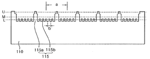
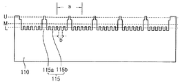
- 1 is a vertical cross-sectional view of a mixed period photonic crystal structure of a light emitting device according to the embodiment
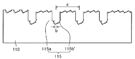
- FIG. 2 is a vertical cross-sectional view of a mixed period photonic crystal structure of a light emitting device according to another embodiment
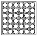
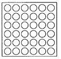
- 3 to 5 are horizontal cross-sectional views of the mixed-cycle photonic crystal structure of the light emitting device according to the embodiment.
- 6 and 7 are tables for the light extraction efficiency of the light emitting device according to the embodiment.
- FIGS. 8 to 14 are process cross-sectional views of a method of manufacturing a light emitting device according to the first embodiment.
- 15 to 17 are process cross-sectional views of a method of manufacturing a light emitting device according to the second embodiment
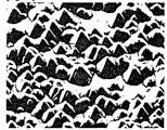
- 18 and 19 are surface photographs of the GaN electron microscope subjected to wet etching immediately after substrate removal.
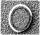
- FIG. 22 and FIG. 23 are electron microscope surface photographs when dry etching is performed using an etching mask as in Example, and wet etching is performed after removing the etching mask.
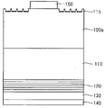
- FIG. 24 is a sectional view of a light emitting device according to a third embodiment
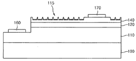
- 25 is a sectional view of a light emitting device according to a fourth embodiment.
- each layer (film), region, pattern or structure may be “on / over” of the substrate, each layer (film), region, pad or patterns or “.
- “on” and “under” are “directly” or “indirectly through another layer.” “Includes all that are formed.
- the criteria for the top or bottom of each layer will be described with reference to the drawings.
- each layer is exaggerated, omitted, or schematically illustrated for convenience and clarity of description.
- the size of each component does not necessarily reflect the actual size.
- FIG. 1 is a vertical cross-sectional view of the mixed-cycle photonic crystal structure of the light emitting device according to the embodiment
- FIGS. 3 to 5 are horizontal cross-sectional views of the mixed-cycle photonic crystal structure of the light emitting device according to the embodiment of FIG. 1 illustrates an example in which a second photonic crystal structure 115b having a second period of a mixed period photonic crystal structure has a constant second period b
- FIG. 2 has a second period b ′ of a mixed period photonic crystal structure.
- the second photonic crystal structure 115b ' has an inconsistent second period b'.
- the mixing cycle photonic crystal structure of FIG. 1 will be described, but the present invention is not limited thereto.
- the mixed-cycle photonic crystal structure refers to a structure filled with a second photonic crystal structure with a small period in the space of the first photonic crystal structure with a large period. Such a mixed-cycle photonic crystal structure is very difficult to realize by a general lithography method.
- the holes or unevenness of the surface in the embodiment has a spatial periodicity, it is called a photonic crystal.
- Several structural factors describing the photonic crystal are closely related to extraction efficiency. That is, the period, the etch depth, the size of the hole, the arrangement of the grid, and the like.
- the angle of incidence of effective diffraction efficiency is determined according to the period of the photonic crystal. Therefore, in the case of a mixed structure in which several cycles are mixed, a high diffraction efficiency can be maintained for various incidence angles compared to the photonic crystal having one cycle. This leads to an increase in extraction efficiency.
- FIG. 1 shows a mixed-cycle photonic crystal in which a second photonic crystal structure 115b having a second period b is disposed between the spaces of the first photonic crystal structure 115a having a first period a of about 1800 nm. Structure 115 is shown.
- 3 to 5 are horizontal cross-sectional views of the mixing cycle photonic crystal structure of the light emitting device according to the embodiment, which is a horizontal cross-sectional view along the U (Upper), M (Middle), and L (Lower) lines of FIG.
- the characteristics of the photonic crystal structure are well understood.
- 6 and 7 are tables for the light extraction efficiency of the light emitting device according to the embodiment.
- 6 and 7 are calculation results showing that the mixed-cycle photonic crystal structure shows superior extraction efficiency compared to the single-cycle photonic crystal structure.
- the S graph shows extraction efficiency according to the radius of holes (unit is a) of the photonic crystal structure for a single period of 1800 nm
- line 115 represents the extraction efficiency of the mixed period photonic crystal structure, respectively.
- the mixed-cycle photonic crystal structure 115 as shown in FIG. 1 or 2 always shows excellent efficiency regardless of the size of the hole of the photonic crystal structure compared to the single-cycle photonic crystal structure S having a period of 1800 nm.
- line 115 represents extraction efficiency according to the period of the second photonic crystal structure that is additionally introduced when the second photonic crystal structure of the second period having a different period is additionally introduced into the first photonic crystal structure.
- the X axis represents the second period b of the second photonic crystal structure.
- the efficiency varies depending on the second period of the second photonic crystal structure to be introduced. If the first period of the first photonic crystal structure is fixed at 1800 nm, and the radius of holes of the first photonic crystal structure is 0.40a, the second period of the second photonic crystal structure is additionally introduced as shown in FIG. 7. The efficiency changes accordingly.
- the second period of the second photonic crystal structure to be introduced may have a maximum efficiency value in the range of approximately 300 ⁇ 650 nm, but is not limited thereto. That is, the second period of the second photonic crystal structure, which may exhibit maximum efficiency, may vary according to the first period of the first photonic crystal structure and the size of the hole.
- the work of filling the space of the first photonic crystal structure of the first period having a large period with the second photonic crystal structure of the second period having a small period should be performed.
- This is difficult to implement by a general lithography method.
- the embodiment defines a first photonic crystal structure by a lithography method and dry etching, and proposes a method of fabricating a mixed cycle photonic crystal structure by forming a second photonic crystal structure through additional wet etching.
- FIGS. 8 to 14 are process cross-sectional views of a method of manufacturing a light emitting device according to the first embodiment.
- the light emitting structure including the first conductive semiconductor layer 110, the active layer 120, and the second conductive semiconductor layer 130 is formed on the first substrate 100.
- the first substrate 100 may be a sapphire (Al 2 O 3 ) single crystal substrate, but is not limited thereto. Impurities on the surface may be removed by performing wet cleaning on the first substrate 100.
- a first conductivity type semiconductor layer 110 is formed on the first substrate 100.
- the first conductivity type semiconductor layer 110 may be formed using a chemical vapor deposition method (CVD), molecular beam epitaxy (MBE), sputtering or hydroxide vapor phase epitaxy (HVPE).
- the first conductive semiconductor layer 110 may include a silane including n-type impurities such as trimethyl gallium gas (TMGa), ammonia gas (NH 3 ), nitrogen gas (N 2 ), and silicon (Si) in the chamber.
- TMGa trimethyl gallium gas
- NH 3 ammonia gas
- N 2 nitrogen gas
- Si silicon
- an active layer 120 is formed on the first conductivity type semiconductor layer 110.
- the active layer 120 is determined by an energy band inherent in the active layer (light emitting layer) material because electrons injected through the first conductive semiconductor layer 110 and holes injected through the second conductive semiconductor layer 130 meet each other. It is a layer that emits light with energy.
- the active layer 120 may have a quantum well structure formed by alternately stacking nitride semiconductor thin films having different energy bands once or several times.
- the active layer 120 is injected with trimethyl gallium gas (TMGa), ammonia gas (NH 3 ), nitrogen gas (N 2 ), and trimethyl indium gas (TMIn) is a multi-quantum well having an InGaN / GaN structure
- TMGa trimethyl gallium gas
- NH 3 ammonia gas
- N 2 nitrogen gas
- TMIn trimethyl indium gas
- a structure may be formed, but is not limited thereto.
- the second conductive semiconductor layer 130 includes p-type impurities such as trimethyl gallium gas (TMGa), ammonia gas (NH 3 ), nitrogen gas (N 2 ), and magnesium (Mg) in the chamber.
- TMGa trimethyl gallium gas
- NH 3 ammonia gas
- N 2 nitrogen gas
- Mg magnesium
- Bicetyl cyclopentadienyl magnesium (EtCp 2 Mg) ⁇ Mg (C 2 H 5 C 5 H 4 ) 2 ⁇ may be formed by injection, but is not limited thereto.
- a second electrode layer 140 may be formed on the second conductive semiconductor layer 130.
- the second electrode layer 140 may include an ohmic layer, a reflective layer, a bonding layer, a second substrate, and the like.
- the second electrode layer 140 may include an ohmic layer, and may be formed by stacking multiple single metals or metal alloys to efficiently inject holes.
- the ohmic layer is a metal oxide or a material containing a metal, for example, ITO, IZO (In-ZnO), GZO (Ga-ZnO), AZO (Al-ZnO), AGZO (Al-Ga ZnO), IGZO (In-Ga ZnO), IrOx, RuOx, RuOx / ITO, Ni / IrOx / Au, and Ni / IrOx / Au / ITO, but are not limited to these materials.
- the second electrode layer 140 may include a reflective layer and / or a bonding layer.
- the reflective layer may be made of Al, Ag, or a metal layer including an alloy including Al or Ag. Aluminum or silver can effectively reflect the light generated from the active layer to greatly improve the light extraction efficiency of the light emitting device.
- the reflective layer may function as a bonding layer, or may form a bonding layer using nickel (Ni), gold (Au), or the like. .
- the second electrode layer 140 may include a second substrate 200. If the first conductivity type semiconductor layer 110 is sufficiently thick (50 ⁇ m or more), the process of forming the second substrate 200 may be omitted.
- the second substrate 200 may be made of a metal, a metal alloy, or a conductive semiconductor material having excellent electrical conductivity to efficiently inject holes.
- the second substrate 200 may be at least one of copper (Cu), copper alloy (Cu Alloy), or Si, Mo, SiGe.
- an electrochemical metal deposition method or a bonding method using a eutectic metal may be used.
- the first substrate 100 is removed to expose the first conductivity-type semiconductor layer 110.
- the first substrate 100 may be removed by using a high-power laser (laser lift-off) to separate the first substrate 100 or use a chemical etching method. In addition, the first substrate 100 may be removed by physically grinding. The removal of the first substrate 100 exposes the first conductivity type semiconductor layer 110. The exposed first conductive semiconductor layer 110 may have a surface defect layer generated when the first substrate 100 is removed. This surface defect layer may be removed by a wet or dry etching method.
- a mixed period photonic crystal structure is formed in a portion R of the exposed first conductive semiconductor layer 110.
- the partial region R of the first conductivity type semiconductor layer 110 may be both sides of the first electrode 160 to be formed later.
- the light emitting device when the rough surface is applied to the electrode (electrode) is applied in the fabrication of the device to which the mixed cycle photonic crystal structure, which is surface unevenness, additional light loss is applied to solve this problem. It is possible to provide a structure in which a mixed-cycle photonic crystal structure is formed in the region R and the electrode region is kept in a plane.
- a first pattern 310 is formed in a portion of the exposed first conductive semiconductor layer 110.
- the first pattern 310 may be a dielectric such as SiO 2 , Si 3 N 4 , or a metal such as Cr or Ni, which is wetted by N-type GaN in a subsequent process. It may be a material that does not cause a reaction in a basic solution such as KOH, NaOH and the like used for etching.
- the first photonic crystal structure 115a having the first period is dry-etched by partially etching the region R of the first conductivity-type semiconductor layer 110 using the first pattern 310 as a mask.
- the first period may be 400-3,000 nm, but is not limited thereto.
- the first pattern 310 is used as a mask in a portion of the first conductivity-type semiconductor layer 110 in which the first photonic crystal structure 115a is formed without removing the first pattern 310.
- the second photonic crystal structure 115b having the second period may be formed by wet etching.
- the second period may be a period smaller than the first period. For example, when the first period is 400 to 3,000 nm, the second period may be 100 to 800 nm.
- the surface where the first pattern mask is not covered has roughness, and the height of the hole (or pillar) is further increased. Deepens.
- the second photonic crystal structure may also be formed in the form of a second period that is not constant as shown in FIG. 2.
- the first electrode layer 150 is formed in a region other than a partial region in which the mixing cycle photonic crystal structure 115 of the first conductive semiconductor layer 110 is formed.
- the first electrode 150 may further include an ohmic layer, a reflective layer, a bonding layer, and the like.
- the first embodiment may further include an undoped semiconductor layer 112 on the first conductivity type semiconductor layer 110 as shown in FIG. 14, and the photonic crystal structure 115 may be formed on the undoped semiconductor layer 112. have.
- an undoped GaN layer 112 may be formed on the first conductive semiconductor layer 110, and a photonic crystal structure 115 may be formed on the undoped GaN layer 112.
- 15 to 17 are process cross-sectional views of a method of manufacturing a light emitting device according to the second embodiment.
- the second embodiment removes the first pattern 310 and performs wet etching.
- a first pattern 310 is formed in a portion of the first conductive semiconductor layer 110, and the first pattern 310 is used as a mask as shown in FIG. 16.
- a portion of the conductive semiconductor layer 110 is dry etched to form a first photonic crystal structure 115a having a first period.
- the first pattern 310 is removed, and a second period having a second period b is formed in a portion of the first conductivity-type semiconductor layer 110 in which the first photonic crystal structure 115a is formed, as shown in FIG. 17.
- the photonic crystal structure 115b can be formed.
- the second photonic crystal structure may also be formed on the surface of the first photonic crystal structure 115a.
- the second period (b) may be a period smaller than the first period (a).
- the second period may be 100 to 800 nm.
- wet etching is performed by removing the mask of the first pattern 310 as shown in FIG. 16, in practice, wet etching of the N-type GaN on which the first pattern 310 is placed is somewhat delayed. This is because, for example, finely stacked Ga ions prevent the wet etching process while the sapphire substrate is removed through a laser lift-off process. Therefore, even if the first pattern mask is removed, surface roughness of 100 to 300 nm may be formed over the photonic crystal surface. That is, the second photonic crystal structure formed on the first photonic crystal structure 115a in which the first pattern 310 was present has a second period that is finer than the second photonic crystal structure formed between the first photonic crystal structure 115a. A second photonic crystal structure can be formed.
- the mixed cycle photonic crystal structure 115 may be completed through the method of the first or second embodiment.
- the GaN surface of the portion where the mask of the first pattern 310 is placed does not react at all to the wet etching process but delays the wet etching to form a fine second roughness of 100 to 300 nm. Is that. Therefore, the surface roughness is eventually covered by wet etching the entire photonic crystal crystal, which may lead to improved extraction efficiency.
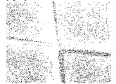
- 18 and 19 are surface photographs of GaN electron microscopes subjected to wet etching immediately after removing a sapphire substrate, for example, a laser lift-off process.
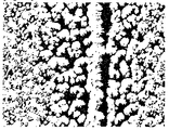
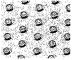
- 20 and 21 are wet etching-treated GaN electron microscope photographs of a part of the GaN surface after dry etching.
- the undoped-GaN layer 112 from which the sapphire substrate is removed or the N-type GaN layer 110 are used.
- Wet etching is performed on the surface.
- wet etching is performed immediately after the substrate is removed as shown in FIGS. 18 and 19, except for the laser lift-off line, the wet etching is performed in addition to the fine surface roughness. It is not active.
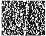
- 22 and 23 are electron microscope surface photographs when dry etching is performed using an etching mask as in Example, and wet etching is performed after removing the etching mask.
- fine surface roughness fills the entire photonic crystal space as shown in FIGS. 22 and 23. Due to the difference in the degree of wet etching depending on the exposure to dry etching, the photonic crystal structure is not collapsed or covered with surface roughness.
- the first photonic crystal may be formed by a general lithography method and dry etching
- the second photonic crystal may be formed by additional wet etching to manufacture a mixed cycle photonic crystal structure.
- the embodiment can increase the light extraction efficiency by having a mixed-cycle photonic crystal structure. That is, the mixed-cycle photonic crystal structure produced according to the embodiment exhibits excellent light extraction efficiency characteristics compared to the light extraction structure consisting of a single-cycle photonic crystal structure or surface roughness.
- FIG. 24 is a cross-sectional view of a light emitting device according to the third embodiment.
- the light emitting device includes a light emitting structure including a first conductive semiconductor layer 110, an active layer 120, and a second conductive semiconductor layer 140, and a conductive substrate 100a on the light emitting structure. And a mixed period photonic crystal structure 115 formed in a portion of the conductive substrate 100a.
- the third embodiment can employ the technical features of the first and second embodiments. Unlike the first and second embodiments, the third embodiment includes a light emitting structure including a first conductive semiconductor layer 110, an active layer 120, and a second conductive semiconductor layer 140 on the conductive substrate 100a.
- the vertical LED structure formed is characterized in that it is not necessary to remove the substrate in the manufacturing method.
- a conductive substrate may be employed, and the mixed period photonic crystal structure 115 may be formed on a portion of the conductive substrate.
- FIG. 24 is mainly different from the first and second embodiments.
- the conductive substrate 100a is prepared.
- the conductive substrate 100a may have excellent electrical conductivity and transparent characteristics in the visible light region.
- the conductive substrate 100a may be a substrate made of gallium nitride (eg, GaN), gallium oxide (eg, Ga 2 O 3 ), zinc oxide (ZnO), silicon carbide (SiC), or metal oxide.
- a light emitting structure including a first conductive semiconductor layer 110, an active layer 120, and a second conductive semiconductor layer 130 is formed on the conductive substrate 100a as in the first and second embodiments. do.
- a part of the lower side of the conductive substrate 100a is removed.
- a polishing process for thinning the lower layer of the conductive substrate 100a is performed.
- the thickness of the conductive substrate 100a thinned by polishing can be appropriately determined according to the application of the device to be manufactured.
- the conductive substrate 100a formed to have a thickness of about 400 to 500 ⁇ m may be polished to leave a thickness of about 70 to 100 ⁇ m, but is not limited thereto.
- the surface crystal quality of the lower surface of the conductive substrate 100a decreases due to high thin film growth temperature and reactive gases. Therefore, polishing the lower layer of the conductive substrate 100a may improve the electrical characteristics of the device.
- the mixed period photonic crystal structure 115 may be formed in a portion of the conductive substrate 100a as in the first or second embodiment.
- the first electrode 150 may be formed in a region other than the partial region in which the mixing period photonic crystal structure 115 of the conductive substrate 100a is formed.
- 25 is a cross-sectional view of a light emitting device according to the fourth embodiment.
- the light emitting device includes a non-conductive substrate 100, a first conductive semiconductor layer 110, an active layer 120, and a second conductive semiconductor layer 140 on the non-conductive substrate 100. And a mixed cycle photonic crystal structure 115 formed in a portion of the second conductive semiconductor layer 140.
- the second electrode 170 may be formed on the second conductive semiconductor layer 140, and the first electrode 160 may be formed on the first conductive semiconductor layer 110.
- the fourth embodiment can employ the technical features of the first to third embodiments. Unlike the first to third embodiments, the fourth embodiment may have a side type LED structure, and may include a mixed period photonic crystal structure 115 on the second conductive semiconductor layer 140.
- the light emitting device exhibits excellent light extraction efficiency characteristics compared to the light extraction structure consisting of a single-cycle photonic crystal structure or surface roughness.
Landscapes
- Led Devices (AREA)
Abstract
실시예는 발광소자에 관한 것이다. 실시예에 따른 발광소자는 제1 도전형 반도체층, 활성층, 제2 도전형 반도체층을 포함하는 발광구조물; 및 상기 발광구조물 상에 혼합주기 광결정 구조;를 포함한다.
Description
실시예는 발광소자에 관한 것이다.
발광소자(Light Emitting Device:LED)는 전류를 빛으로 변환시키는 반도체소자로서, 적색 LED가 상품화된 것을 시작으로 녹색 LED와 함께 정보 통신기기를 비롯한 전자장치의 광원으로 이용되어 왔다.
예를 들어, Gallium Nitride(GaN) 반도체 등의 질화물 반도체는 높은 열적 안정성과 폭넓은 밴드갭에 의해 광소자 및 고출력 전자소자 개발 분야에서 활발히 연구되고 있으며, 현재 질화물 반도체 발광소자의 연구는 발광효율 향상에 주력하고 있다.
반도체 박막 관점에서 고효율의 발광소자 구현을 위해서는 (1) 발광층에서 주입된 전자와 정공의 발광 결합확률을 증대시킴으로서 내부양자효율을 개선하는 방법과 (2) 발광층에서 형성된 빛이 효과적으로 박막 밖으로 빠져나올 수 있도록 광추출 효율을 증대시키는 방법이 필수적으로 요구된다.
내부양자효율을 개선하기 위해서는 고품질의 박막을 성장하는 기술과 양자효과를 극대화 할 수 있도록 박막 적층구조를 최적화 하는 기술이 요구되며, 광추출효율을 증대시키기 위하여서는 반도체박막의 기하학적 형상 제어에 대하여 많은 연구가 진행되고 있다.
실시예는 광추출 효율이 우수한 발광소자를 제공하고자 한다.
실시예에 따른 발광소자는 제1 도전형 반도체층, 활성층, 제2 도전형 반도체층을 포함하는 발광구조물; 및 상기 발광구조물 상에 혼합주기 광결정 구조;를 포함한다.
또한, 실시예에 따른 발광소자는 제1 도전형 반도체층, 활성층, 제2 도전형 반도체층을 포함하는 발광구조물; 상기 발광구조물 아래에 도전성 기판; 및 상기 도전성 기판에 형성된 혼합주기 광결정 구조;를 포함한다.
실시예에 따른 발광소자에 의하면 단일주기 광결정구조 또는 표면 거칠기로 이루어지는 광추출 구조에 비해 우수한 광 추출효율 특성을 나타낸다.
도 1은 실시예에 따른 발광소자의 혼합주기 광결정구조의 수직 단면도.
도 2는 다른 실시예에 따른 발광소자의 혼합주기 광결정구조의 수직 단면도.
도 3 내지 도 5는 실시예에 따른 발광소자의 혼합주기 광결정구조의 수평 단면도.
도 6 및 도 7은 실시예에 따른 발광소자의 광추출 효율에 대한 표.
도 8 내지 도 14는 제1 실시예에 따른 발광소자의 제조방법의 공정단면도.
도 15 내지 도 17은 제2 실시예에 따른 발광소자의 제조방법의 공정단면도.
도 18 및 도 19는 기판 제거 직후 습식식각 처리한 GaN 전자현미경 표면사진.
도 20 및 21은 GaN 표면 일부를 건식식각 후 습식식각 처리 GaN 전자현미경표면사진.
도 22 및 도 23은 실시예와 같이 식각 마스크(mask)를 이용하여 건식식각하고, 식각 마스크(mask) 제거 후 습식식각을 실시하였을 때의 전자현미경 표면사진.
도 24는 제3 실시예에 따른 발광소자의 단면도.
도 25는 제4 실시예에 따른 발광소자의 단면도.
이하에서 첨부된 도면을 참조하여 실시예를 상세히 설명한다.
본 발명에 따른 실시 예의 설명에 있어서, 각 층(막), 영역, 패턴 또는 구조물들이 기판, 각 층(막), 영역, 패드 또는 패턴들의 "상(on)/위(over)"에 또는 "아래(under)"에 형성되는 것으로 기재되는 경우에 있어, "상(on)/위(over)"와 "아래(under)"는 "직접(directly)" 또는 "다른 층을 개재하여 (indirectly)" 형성되는 것을 모두 포함한다. 또한 각 층의 위 또는 아래에 대한 기준은 도면을 기준으로 설명한다.
도면에서 각층의 두께나 크기는 설명의 편의 및 명확성을 위하여 과장되거나 생략되거나 또는 개략적으로 도시되었다. 또한 각 구성요소의 크기는 실제크기를 전적으로 반영하는 것은 아니다.
(실시예)
도 1은 실시예에 따른 발광소자의 혼합주기 광결정구조의 수직 단면도이며, 도 3 내지 도 5는 도 1의 실시예에 따른 발광소자의 혼합주기 광결정구조의 수평 단면도이다. 도 1은 혼합주기 광결정구조 중 제2 주기를 가지는 제2 광결정 구조(115b)가 일정한 제2 주기(b)를 가지는 예이며, 도 2는 혼합주기 광결정구조 중 제2 주기(b')를 가지는 제2 광결정 구조(115b')가 일정하지 않은 제2 주기(b')를 가지는 예이다. 이하 도 1의 혼합주기 광결정구조를 중심으로 설명하나 본 발명이 이에 한정된 것은 아니다.
혼합 주기 광결정(Photonic Crystal) 구조는 주기가 큰 첫 번째 광결정 구조의 공간 내를 주기가 작은 두 번째 광결정 구조로 채워진 구조를 의미한다. 이러한, 혼합 주기 광결정 구조는 일반적인 사진공정(Lithography) 방법으로 구현하기는 매우 힘들다.
LED 발광 효율 향상을 위해 표면 요철 공정은 필수적이다. 표면 요철은 LED 내부에 전반사 과정에 의해 갇혀 있는 빛을 회절을 통해 외부로 추출하는 역할을 한다.
실시예에서 표면의 홀 또는 요철이 공간적인 주기성을 가질 때, 이를 광결정(Photonic Crystal)이라 한다. 광결정을 묘사하는 여러 구조 인자들은 추출효율과 밀접한 관련이 있다. 즉, 주기, 식각 깊이, 구멍의 크기, 격자의 배열 등이 이에 해당한다.
특히, 광결정의 주기에 따라 회절효율이 효과적인 입사 각도가 정해져 있으며, 따라서 여러 주기가 섞여 있는 혼합 구조의 경우 하나의 주기로 이루어진 광결정에 비해 다양한 입사 각도에 대해 높은 회절 효율을 유지할 수 있다. 이는 곧, 추출효율의 상승으로 이어진다.
도 1은 제1 주기(a)인 약 1800 nm의 제1 광결정 구조(115a)의 공간 사이에 제2 주기(b)인 약 250 nm의 제2 광결정 구조(115b)가 배치되어 있는 혼합주기 광결정 구조(115)를 나타낸다.
도 3 내지 도 5는 실시예에 따른 발광소자의 혼합주기 광결정구조의 수평 단면도로서, 상기 도 1의 U(Upper), M(Middle), L(Lower) 선을 따른 수평단면도로, 이러한 혼합주기 광결정구조의 특성을 잘 알 수 있다.
도 6 및 도 7은 실시예에 따른 발광소자의 광추출 효율에 대한 표이다.
도 6 및 도 7은 혼합주기 광결정구조가 단일주기 광결정 구조에 비해 우수한 추출효율을 나타낸다는 것을 보여주는 계산 결과이다.
먼저, 도 6를 살펴보면, S 그래프는 1800nm 단일주기에 대해 광결정구조의 구멍 크기(Radius of Holes)(단위는 a임)에 따른 추출효율이며, 115선은 혼합주기 광결정구조의 추출효율을 각각 나타낸다. 도 1 또는 도 2와 같은 혼합주기 광결정구조(115)가 주기 1800nm의 단일주기 광결정 구조(S)에 비해 광결정 구조의 구멍의 크기에 관계 없이 항상 우수한 효율을 나타낸다.
도 7에서 115선은 제1 주기 1800nm 제1 광결정 구조 내부에 주기가 다른 제2 주기의 제2 광결정 구조가 추가적으로 도입될 때, 추가 도입되는 제2 광결정 구조의 주기에 따른 추출효율을 나타낸다. 도 7에서 X축은 제2 광결정 구조의 제2 주기(b)를 의미한다.
도 7에서 볼수 있듯이, 추가적으로 도입되는 제2 광결정 구조의 제2 주기에 따라 효율이 변한다는 것을 알 수 있다. 만약, 제1 광결정 구조의 제1 주기가 1800nm로 고정되어 있고, 제1 광결정구조의 구멍 크기(Radius of Holes)가 0.40a인 경우 도 7과 같이 추가적으로 도입되는 제2 광결정 구조의 제2 주기에 따라 효율이 변한다. 상기와 같은 제1 광결정구조의 조건의 경우에, 추가적으로 도입되는 제2 광결정 구조의 제2 주기는 대략 300~650 nm의 범위에서 최대 효율값을 가질 수 있으나 이에 한정되는 것은 아니다. 즉, 제1 광결정 구조의 제1 주기와 구멍의 크기에 따라 최대 효율을 나타낼 수 있는 제2 광결정 구조의 제2 주기는 변화될 수 있다.
한편, 혼합주기 광결정구조를 제작하기 위해서는 주기가 큰 제1 주기의 제1 광결정 구조의 공간 내를 주기가 작은 제2 주기의 제2 광결정 구조로 채우는 작업을 실행해야 한다. 이는, 일반적인 사진공정(Lithography) 방법으로 구현하기는 힘든 점이 있다. 실시예는 사진공정(Lithography) 방법과 건식식각으로 제1 광결정 구조를 정의하고, 추가적인 습식식각을 통해 제2 광결정구조를 형성하여 혼합주기 광결정구조를 제작하는 방법을 제안하고자 한다.
도 8 내지 도 14는 제1 실시예에 따른 발광소자의 제조방법의 공정단면도이다.
먼저, 도 8과 같이 제1 기판(100) 상에 제1 도전형 반도체층(110), 활성층(120), 제2 도전형 반도체층(130)을 포함하는 발광구조물을 형성한다.
상기 제1 기판(100)은 사파이어(Al2O3) 단결정 기판일 수 있으나 이에 한정되는 것은 아니다. 상기 제1 기판(100)에 대해 습식세척을 실시하여 표면의 불순물을 제거할 수 있다.
이후, 상기 제1 기판(100) 상에 제1 도전형 반도체층(110)을 형성한다. 예를 들어, 상기 제1 도전형 반도체층(110)은 화학증착방법(CVD) 혹은 분자선 에피택시 (MBE) 혹은 스퍼터링 혹은 수산화물 증기상 에피택시(HVPE) 등의 방법을 사용하여 형성할 수 있다. 또한, 상기 제1 도전형 반도체층(110)은 챔버에 트리메틸 갈륨 가스(TMGa), 암모니아 가스(NH3), 질소 가스(N2), 및 실리콘(Si)와 같은 n 형 불순물을 포함하는 실란 가스(SiH4)가 주입되어 형성될 수 있다.
다음으로, 상기 제1 도전형 반도체층(110) 상에 활성층(120)을 형성한다. 상기 활성층(120)은 제1 도전형 반도체층(110)을 통해서 주입되는 전자와 제2 도전형 반도체층(130)을 통해서 주입되는 정공이 서로 만나서 활성층(발광층) 물질 고유의 에너지 밴드에 의해서 결정되는 에너지를 갖는 빛을 방출하는 층이다. 활성층(120)은 에너지 밴드가 서로 다른 질화물 반도체 박막층을 교대로 한 번 혹은 여러 번 적층하여 이루어지는 양자우물구조를 가질 수 있다. 예를 들어, 상기 활성층(120)은 트리메틸 갈륨 가스(TMGa), 암모니아 가스(NH3), 질소 가스(N2), 및 트리메틸 인듐 가스(TMIn)가 주입되어 InGaN/GaN 구조를 갖는 다중 양자우물구조가 형성될 수 있으나 이에 한정되는 것은 아니다.
이후, 상기 활성층(120) 상에 제2 도전형 반도체층(130)을 형성한다. 예를 들어, 상기 제2 도전형 반도체층(130)은 챔버에 트리메틸 갈륨 가스(TMGa), 암모니아 가스(NH3), 질소 가스(N2), 및 마그네슘(Mg)과 같은 p 형 불순물을 포함하는 비세틸 사이클로 펜타디에닐 마그네슘(EtCp2Mg){Mg(C2H5C5H4)2}가 주입되어 형성될 수 있으나 이에 한정되는 것은 아니다.
다음으로, 상기 제2 도전형 반도체층(130) 상에 제2 전극층(140)을 형성할 수 있다. 상기 제2 전극층(140)은 오믹층, 반사층, 결합층, 제2 기판 등을 포함할 수 있다.
예를 들어, 상기 제2 전극층(140)은 오믹층을 포함할 수 있으며, 정공주입을 효율적으로 할 수 있도록 단일 금속 혹은 금속합금 등을 다중으로 적층하여 형성할 수 있다. 또한, 상기 오믹층은 금속산화물 또는 금속을 포함하는 물질, 예를 들면 ITO, IZO(In-ZnO), GZO(Ga-ZnO), AZO(Al-ZnO), AGZO(Al-Ga ZnO), IGZO(In-Ga ZnO), IrOx, RuOx, RuOx/ITO, Ni/IrOx/Au, 및 Ni/IrOx/Au/ITO 중 적어도 하나를 포함할 수 있으며, 이러한 재료에 한정되는 않는다.
또한, 상기 제2 전극층(140)은 반사층 및/또는 결합층을 포함할 수 있다. 예를 들어, 상기 제2 전극층(140)이 반사층을 포함하는 경우 반사층은 Al, Ag, 혹은 Al이나 Ag를 포함하는 합금을 포함하는 금속층으로 이루어질 수 있다. 알루미늄이나 은 등은 활성층에서 발생된 빛을 효과적으로 반사하여 발광소자의 광추출 효율을 크게 개선할 수 있다.
또한, 예를 들어, 상기 제2 전극층(140)이 결합층을 포함하는 경우 상기 반사층이 결합층의 기능을 하거나, 니켈(Ni), 금(Au) 등을 이용하여 결합층을 형성할 수 있다.
또한, 실시예에서 제2 전극층(140)은 제2 기판(200)을 포함할 수 있다. 만약, 상기 제1 도전형 반도체층(110)이 50㎛ 이상으로 충분히 두꺼운 경우에는 제2 기판(200)을 형성하는 공정은 생략될 수 있다.
상기 제2 기판(200)은 효율적으로 정공을 주입할 수 있도록 전기 전도성이 우수한 금속, 금속합금, 혹은 전도성 반도체 물질로 이루어질 수 있다. 예를 들어, 상기 제2 기판(200)은 구리(Cu), 구리합금(Cu Alloy) 또는 Si, Mo, SiGe 중 적어도 하나일 수 있다. 상기 제2 기판(200)을 형성시키는 방법은 전기화학적인 금속증착방법이나 공융금속을 이용한 본딩 방법 등을 사용할 수 있다.
다음으로, 도 9와 같이 상기 제1 도전형 반도체층(110)이 노출되도록 상기 제1 기판(100)을 제거한다.
상기 제1 기판(100)을 제거하는 방법은 고출력의 레이저를 이용(laser lift-off)하여 제1 기판(100)을 분리하거나 화학적 식각 방법을 사용할 수 있다. 또한, 상기 제1 기판(100)은 물리적으로 갈아냄으로써 제거할 수도 있다. 상기 제1 기판(100)의 제거는 제1 도전형 반도체층(110)을 노출시킨다. 상기 노출된 제1 도전형 반도체층(110)은 제1 기판(100) 제거시 발생되는 표면 결함층을 갖을 수 있다. 이러한 표면 결함층은 습식 혹은 건식 식각 방법으로 제거할 수 있다.
다음으로, 상기 노출된 제1 도전형 반도체층(110)의 일부 영역(R)에 혼합주기 광결정 구조를 형성한다. 상기 제1 도전형 반도체층(110)의 일부 영역(R)은 이후 형성될 제1 전극(160)의 양측이 될 수 있다.
한편, 실시예에 따른 발광소자에 의하면, 표면 요철인 혼합주기 광결정 구조를 적용한 소자제작에 있어서 전극(electrode)에 거친면이 적용될 경우에는 추가적인 광손실을 주기 때문에 이를 해결하기 위해서 도 9와 같이 일정한 영역(R)에 혼합주기 광결정 구조를 형성하고, 전극(electrode)영역을 평면으로 유지시키는 구조를 제공할 수 있다.
이하, 도 10 내지 도 12를 참조하여 상기 제1 도전형 반도체층(110)의 일부 영역(R)에 혼합주기 광결정 구조를 형성하는 공정을 구체적으로 설명한다.
먼저, 도 10와 같이 상기 노출된 제1 도전형 반도체층(110)의 일부 영역에 제1 패턴(310)을 형성한다. 상기 제1 패턴(310)은 건식식각을 위해 사용되는 마스크(mask)로서 SiO2, Si3N4 등의 유전체, 또는 Cr, Ni 등의 금속이 가능하며, 이는 후속공정에서 N형 GaN의 습식 식각에 사용되는 KOH, NaOH 등과 같은 염기성 용액에 반응을 일으키지 않는 물질일 수 있다.
이후, 도 11와 같이 상기 제1 패턴(310)을 마스크로 하여 상기 제1 도전형 반도체층(110)의 일부 영역(R)을 건식식각하여 제1 주기를 가지는 제1 광결정 구조(115a)를 형성한다. 상기 제1 주기는 400~3,000nm일 수 있으나 이에 한정되는 것은 아니다.
이후, 도 12와 같이 상기 제1 패턴(310)을 제거하지 않고 상기 제1 광결정 구조(115a)가 형성된 제1 도전형 반도체층(110)의 일부 영역에 상기 제1 패턴(310)을 마스크로 습식식각하여 제2 주기를 가지는 제2 광결정 구조(115b)를 형성할 수 있다. 상기 제2 주기는 상기 제1 주기 보다 작은 주기일 수 있다. 예를 들어, 상기 제1 주기는 400~3,000nm인 경우, 상기 제2 주기는 100~800nm일 수 있다.
건식 식각을 마친 후, 제1 패턴 마스크(mask)를 제거하지 않은 채 습식 식각을 실시하면, 제1 패턴 마스크(mask)가 덮여있지 않는 표면은 거칠기가 형성되며, 구멍 (혹은 기둥)의 높이는 더욱 깊어진다.
이때, 실시예에서 제2 광결정구조는 도 2와 같이 일정하지 않은 제2 주기 형태로도 형성할 수도 있다.
다음으로, 도 13과 같이 상기 제1 도전형 반도체층(110)의 혼합주기 광결정구조(115)가 형성된 일부 영역 외의 영역에 제1 전극층(150)을 형성한다. 상기 제1 전극(150)은 오믹층, 반사층, 결합층 등을 더 포함할 수 있다.
도 14는 제1 실시예에 따른 발광소자의 다른 실시예의 단면도이다. 제1 실시예는 도 14와 같이 제1 도전형 반도체층(110) 상에 언도프트 반도체층(112)을 더 포함하고, 광결정 구조(115)가 상기 언도프트 반도체층(112)에 형성될 수 있다. 예를 들어, 제1 도전형 반도체층(110) 상에 undoped GaN 층(112)을 형성하고, 상기 undoped GaN 층(112)에 광결정 구조(115)를 형성할 수 있다.
(제2 실시예)
도 15 내지 도 17은 제2 실시예에 따른 발광소자의 제조방법의 공정단면도이다.
제2 실시예는 제1 실시예와 달리 제1 패턴(310)을 제거하고, 습식식각을 진행하는 예이다. 예를 들어, 도 15와 같이 상기 제1 도전형 반도체층(110)의 일부 영역에 제1 패턴(310)을 형성하고, 도 16과 같이 상기 제1 패턴(310)을 마스크로 하여 상기 제1 도전형 반도체층(110)의 일부 영역을 건식식각하여 제1 주기를 가지는 제1 광결정 구조(115a)를 형성한다. 이후, 상기 제1 패턴(310)을 제거하고, 도 17과 같이 상기 제1 광결정 구조(115a)가 형성된 제1 도전형 반도체층(110)의 일부 영역에 제2 주기(b)를 가지는 제2 광결정 구조(115b)를 형성할 수 있다. 한편, 제2 실시예에서 제1 광결정 구조(115a) 표면 상에도 제2 광결정 구조가 형성될 수 있다.
상기 제2 주기(b)는 상기 제1 주기(a) 보다 작은 주기일 수 있다. 예를 들어, 상기 제1 주기가 400~3,000nm인 경우, 상기 제2 주기는 100~800nm일 수 있다.
도 16과 같이 제1 패턴(310) 마스크(mask)를 제거하고 습식식각을 실시하더라도, 실제로는 제1 패턴(310)이 놓여 있던 N형 GaN는 습식식각이 다소 지연되게 된다. 그 이유는 예를 들어, 사파이어(sapphire) 기판을 레이저 리프 오프(laser lift-off) 과정을 통해 제거하면서 미세하게 쌓인 Ga 이온이 습식식각 과정을 막기 때문이다. 따라서, 제1 패턴 마스크(mask)을 제거하더라도 광결정 표면 곳곳에는 크기 100~300 nm의 표면 거칠기가 형성될 수 있다. 즉, 제1 패턴(310)이 존재하던 제1 광결정 구조(115a) 상에 형성되는 제2 광결정 구조는 제1 광결정 구조(115a) 사이에 형성되는 제2 광결정 구조 보다 좀 더 미세한 제2 주기의 제2 광결정 구조가 형성될 수 있다.
이러한 제1 실시예 또는 제2 실시예의 방법을 통해서 일종의 혼합주기 광결정구조(115)를 완성할 수 있다. 한편, 제1 패턴(310) 마스크(mask)가 놓여 있는 부분의 GaN 표면은 습식식각 과정에 전혀 반응을 하지 않는 것이 아니라 습식식각을 지연시킴으로써 100~300 nm 크기의 미세한 제2 주기의 거칠기를 형성한다는 것이다. 따라서, 결국은 광결정 전체 영역을 습식 식각을 통해 표면 거칠기가 덮게 되어, 향상된 추출효율을 이끌어 낼 수 있다.
도 18 및 도 19는 사파이어(sapphire) 기판을 제거, 예를 들어 레이저 리프 오프(laser lift-off) 과정 직후 습식식각 처리한 GaN 전자현미경 표면사진이다. 또한, 도 20 및 21은 GaN 표면 일부를 건식식각 후 습식식각 처리 GaN 전자현미경표면사진이다.
예를 들어, 상기 제1 실시예, 제2 실시예와 같이 수직형(Vertical type) GaN LED 구조의 경우 사파이어(Sapphire) 기판이 제거된 undoped-GaN 층(112) 또는 N형 GaN층(110) 표면에 습식 식각을 실시하는데, 도 18 및 도 19와 같이 기판 제거 직후 습식식각을 실시하면, 레이저 리프트 오프(Laser lift-off) 라인(line)을 제외하고는 미세한 크기의 표면 거칠기 외에 습식 식각은 활발하게 이루어지지 않는다.
반면에, 도 20 및 21과 같이 GaN 표면의 Ga 이온을 건식식각으로 제거한 뒤, 습식 식각을 실시하면 전자현미경 사진에서 보듯이 적절한 크기의 거칠기 형상이 표면에 균일하게 형성된다.
도 22 및 도 23은 실시예와 같이 식각 마스크(mask)를 이용하여 건식식각하고, 식각 마스크(mask) 제거 후 습식식각을 실시하였을 때의 전자현미경 표면사진이다.
실시예에 의하면 도 22 및 23과 같이 미세한 표면 거칠기가 광결정 공간 전체를 채우고 있다. 건식식각에 노출 여부에 따른 습식식각 반응 정도의 차이로 인해 광결정 구조가 무너지거나 표면 거칠기로 덮이는 경우는 발생하지 않는다.
실시예에 따른 발광소자에 의하면, 일반적인 사진공정(Lithography) 방법과 건식 식각으로 첫 번째 광결정을 형성하고, 추가적인 습식 식각을 통해 두 번째 광결정을 형성하여 혼합주기 광결정 구조를 제작할 수 있다.
또한, 실시예는 혼합주기 광결정 구조를 가짐으로써 광추출 효율을 증대시킬 수 있다. 즉, 실시예에 따라 제작되는 혼합주기 광결정 구조는 단일주기 광결정구조 또는 표면 거칠기로 이루어지는 광추출 구조에 비해 우수한 광 추출효율 특성을 나타낸다.
(제3 실시예)
도 24는 제3 실시예에 따른 발광소자의 단면도이다.
제3 실시예에 따른 발광소자는 제1 도전형 반도체층(110), 활성층(120), 제2 도전형 반도체층(140)을 포함하여 형성된 발광구조물, 상기 발광구조물 상에 도전성 기판(100a) 및 상기 도전성 기판(100a) 일부 영역에 형성된 혼합주기 광결정구조(115)를 포함할 수 있다.
제3 실시예는 상기 제1 실시예 및 제2 실시예의 기술적인 특징을 채용할 수 있다. 제3 실시예는 제1, 제2 실시예와 달리 도전성 기판(100a)에 제1 도전형 반도체층(110), 활성층(120), 제2 도전형 반도체층(140)을 포함하는 발광구조물 이 형성되는 수직형 LED 구조로서 제조방법 상에서 기판을 제거할 필요가 없는 점에 특징이 있다.
즉, 제3 실시예는 도전성 기판을 채용하고, 상기 도전성 기판의 일부에 혼합주기 광결정구조(115)를 형성할 수 있다.
이하, 도 24를 참조하여 제3 실시예에 따른 발광소자의 제조방법을 설명하되 상기 제1 실시예, 제2 실시예와 다른 점을 주로 설명한다.
우선, 도전성 기판(100a)이 준비된다. 상기 도전성 기판(100a)은 전기전도도가 우수하고 가시광선 영역에서 투명한 특성을 가질 수 있다. 상기 도전성 기판(100a)으로는 갈륨질화물(예, GaN), 갈륨산화물(예, Ga2O3), 산화아연(ZnO), 실리콘 카바이드(SiC) 혹은 금속산화물 등으로 이루어진 기판일 수 있다.
이후, 제1, 제2 실시예와 같이 상기 도전성 기판(100a) 상에 제1 도전형 반도체층(110), 활성층(120), 제2 도전형 반도체층(130)을 포함하는 발광구조물을 형성한다.
다음으로, 상기 도전성 기판(100a)의 하측의 일부를 제거한다. 예를 들어, 상기 도전성 기판(100a)의 하부층을 얇게 만드는 폴리싱(polishing) 처리를 실시한다. 폴리싱을 실시하여 얇아지는 도전성 기판(100a)의 두께는 제조하고자 하는 소자의 응용 제품에 따라서 적절히 결정할 수 있다. 예를 들어, 약 400~500㎛로 형성된 도전성 기판(100a)을 폴리싱하여 약 70~100㎛의 두께를 남길 수 있으나 이에 한정되는 것은 아니다.
한편, 도전성 기판(100a) 위에 박막성장장비를 이용하여 고온에서 질화물 반도체 박막을 형성하게 되면 도전성 기판(100a)의 하부면이 높은 박막성장 온도와 반응성 가스들에 의해서 표면 결정 품질이 저하된다. 따라서, 도전성 기판(100a)의 하부층을 폴리싱하는 것이 소자의 전기적 특성을 개선할 수 있다.
다음으로, 상기 도전성 기판(100a)의 일부 영역에 상기 제1 실시예 또는 제2 실시예와 같이 혼합주기 광결정구조(115)를 형성할 수 있다.
다음으로, 상기 도전성 기판(100a)의 상기 혼합주기 광결정구조(115)가 형성된 일부 영역 외의 영역에 제1 전극(150)을 형성할 수 있다.
(제4 실시예)
도 25는 제4 실시예에 따른 발광소자의 단면도이다.
제4 실시예에 따른 발광소자는 비도전성 기판(100), 상기 비도전성 기판(100) 상에 제1 도전형 반도체층(110), 활성층(120), 제2 도전형 반도체층(140)을 포함하여 형성된 발광구조물 및 상기 제2 도전형 반도체층(140) 일부 영역에 형성된 혼합주기 광결정구조(115)를 포함할 수 있다. 상기 제2 도전형 반도체층(140) 상에는 제2 전극(170)이, 상기 제1 도전형 반도체층(110) 상에는 제1 전극(160)이 형성될 수 있다.
제4 실예는 상기 제1 실시예 내지 제3 실시예의 기술적인 특징을 채용할 수 있다. 제4 실시예는 제1 실시예 내지 제3 실시예와 달리 측면형 LED 구조를 가지며, 제2 도전형 반도체층(140) 상에 혼합주기 광결정구조(115)를 포함할 수 있다.
실시예에 따른 발광소자에 의하면 단일주기 광결정구조 또는 표면 거칠기로 이루어지는 광추출 구조에 비해 우수한 광 추출효율 특성을 나타낸다.
이상에서 본 발명에 대하여 그 바람직한 실시예를 중심으로 설명하였으나 이는 단지 예시일 뿐 본 발명을 한정하는 것이 아니며, 본 발명이 속하는 분야의 통상의 지식을 가진 자라면 본 발명의 본질적인 특성을 벗어나지 않는 범위에서 이상에 예시되지 않은 여러 가지의 변형과 응용이 가능함을 알 수 있을 것이다. 예를 들어, 본 발명의 실시예에 구체적으로 나타난 각 구성 요소는 변형하여 실시할 수 있는 것이다. 그리고 이러한 변형과 응용에 관계된 차이점들은 첨부된 청구 범위에서 규정하는 본 발명의 범위에 포함되는 것으로 해석되어야 할 것이다.
Claims (15)
- 제1 도전형 반도체층, 활성층, 제2 도전형 반도체층을 포함하는 발광구조물; 및상기 발광구조물 상에 혼합주기 광결정 구조;를 포함하는 발광소자.
- 제1 항에 있어서,상기 혼합주기 광결정 구조는,상기 제1 도전형 반도체층의 일부 영역에 제1 주기를 가지는 제1 광결정 구조; 및상기 제1 광결정 구조가 형성된 제1 도전형 반도체층의 일부 영역에 제2 주기를 가지는 제2 광결정 구조;를 포함하는 발광소자.
- 제2 항에 있어서,상기 제2 주기는 상기 제1 주기 보다 작은 주기인 발광소자.
- 제3 항에 있어서,상기 제2 주기는 일정한 주기 또는 일정하지 않은 주기 중 적어도 하나인 발광소자.
- 제3 항에 있어서,상기 제2 주기는 100~800nm 범위 내인 발광소자.
- 제1 항에 있어서,상기 제1 도전형 반도체층 상에 언도프트 반도체층을 포함하는 발광소자.
- 제6 항에 있어서,상기 혼합주기 광결정 구조는상기 언도프트 반도체층의 일부 영역에 제1 주기를 가지는 제1 광결정 구조; 및상기 제1 광결정 구조가 형성된 언도프트 반도체층의 일부 영역에 제2 주기를 가지는 제2 광결정 구조;를 포함하는 발광소자.
- 제1 항에 있어서,상기 발광구조물 아래에 형성된 비도전성 기판을 포함하는 발광소자.
- 제8 항에 있어서,상기 제2 도전형 반도체층에 혼합주기 광결정 구조가 형성되는 발광소자.
- 제1 도전형 반도체층, 활성층, 제2 도전형 반도체층을 포함하는 발광구조물;상기 발광구조물 아래에 도전성 기판; 및상기 도전성 기판에 형성된 혼합주기 광결정 구조;를 포함하는 발광소자.
- 제10 항에 있어서,상기 혼합주기 광결정 구조는,상기 도전성 기판의 일부 영역에 제1 주기를 가지는 제1 광결정 구조; 및상기 제1 광결정 구조가 형성된 도전성 기판의 일부 영역에 제2 주기를 가지는 제2 광결정 구조;를 포함하는 발광소자.
- 제11 항에 있어서,상기 제2 주기는 상기 제1 주기 보다 작은 주기인 발광소자.
- 제11 항에 있어서,상기 제2 주기는 일정한 주기 또는 일정하지 않은 주기 중 적어도 어느 하나인 발광소자.
- 제12 항에 있어서,상기 제1 주기는 400~3,000nm 범위내이고, 상기 제2 주기는 100~800nm 범위 내인 발광소자.
- 제12 항에 있어서,상기 혼합주기 광결정 구조외의 도전성 기판상에 제1 전극을 포함하는 발광소자.
Applications Claiming Priority (2)
| Application Number | Priority Date | Filing Date | Title |
|---|---|---|---|
| KR10-2009-0017997 | 2009-03-03 | ||
| KR1020090017997A KR101134810B1 (ko) | 2009-03-03 | 2009-03-03 | 발광소자 및 그 제조방법 |
Publications (1)
| Publication Number | Publication Date |
|---|---|
| WO2010101332A1 true WO2010101332A1 (ko) | 2010-09-10 |
Family
ID=42101548
Family Applications (1)
| Application Number | Title | Priority Date | Filing Date |
|---|---|---|---|
| PCT/KR2009/003038 Ceased WO2010101332A1 (ko) | 2009-03-03 | 2009-06-05 | 발광소자 |
Country Status (5)
| Country | Link |
|---|---|
| US (2) | US20100224854A1 (ko) |
| EP (1) | EP2226855B1 (ko) |
| KR (1) | KR101134810B1 (ko) |
| CN (1) | CN101826579A (ko) |
| WO (1) | WO2010101332A1 (ko) |
Families Citing this family (15)
| Publication number | Priority date | Publication date | Assignee | Title |
|---|---|---|---|---|
| EP2341558B1 (en) * | 2009-12-30 | 2019-04-24 | IMEC vzw | Method of manufacturing a semiconductor device |
| KR20110135237A (ko) * | 2010-06-10 | 2011-12-16 | 엘지디스플레이 주식회사 | 반도체 발광소자 및 그 제조방법 |
| KR101316619B1 (ko) * | 2011-05-13 | 2013-10-15 | (주)버티클 | 반도체 소자 및 그 제조 방법 |
| KR101969334B1 (ko) | 2011-11-16 | 2019-04-17 | 엘지이노텍 주식회사 | 발광 소자 및 이를 구비한 발광 장치 |
| EP2942822A1 (en) * | 2012-04-02 | 2015-11-11 | Asahi Kasei E-materials Corporation | Optical substrate, semiconductor light-emitting element and method of manufacturing semiconductor light-emitting element |
| KR101373152B1 (ko) * | 2012-06-12 | 2014-03-13 | 순천대학교 산학협력단 | 반도체 발광 소자 및 그 제조 방법 |
| KR102002131B1 (ko) * | 2012-08-03 | 2019-07-22 | 삼성디스플레이 주식회사 | 식각액 조성물 및 이를 이용한 박막 트랜지스터 제조 방법 |
| CN102931308B (zh) * | 2012-11-19 | 2015-05-06 | 中国科学院半导体研究所 | 渐变半径光子晶体发光二极管制备方法 |
| CN103022283B (zh) * | 2012-12-26 | 2015-04-15 | 东南大学 | 一种砷化镓基光子晶体发光二级管的制备方法 |
| CN103337576A (zh) * | 2013-06-09 | 2013-10-02 | 武汉迪源光电科技有限公司 | 图形化衬底及其制造方法、led芯片及其制造方法 |
| US9490182B2 (en) * | 2013-12-23 | 2016-11-08 | Kla-Tencor Corporation | Measurement of multiple patterning parameters |
| CN104009139B (zh) * | 2014-06-11 | 2016-08-24 | 海迪科(南通)光电科技有限公司 | 区域光子晶体发光二极管器件 |
| JP6010169B2 (ja) * | 2015-03-31 | 2016-10-19 | 株式会社東芝 | 半導体発光素子 |
| CN108321275B (zh) * | 2018-01-25 | 2019-09-24 | 山东师范大学 | 一种具有类光栅结构的宽频高光提取led芯片及其制作方法 |
| DE102018106970A1 (de) * | 2018-03-23 | 2019-09-26 | Osram Opto Semiconductors Gmbh | Optoelektronisches Halbleiterbauelement und Verfahren zur Herstellung eines optoelektronischen Halbleiterbauelements |
Citations (3)
| Publication number | Priority date | Publication date | Assignee | Title |
|---|---|---|---|---|
| US20050205883A1 (en) * | 2004-03-19 | 2005-09-22 | Wierer Jonathan J Jr | Photonic crystal light emitting device |
| KR20070117336A (ko) * | 2006-06-08 | 2007-12-12 | 엘지전자 주식회사 | 수평형 발광 소자 및 그 제조방법 |
| KR20080093558A (ko) * | 2007-04-17 | 2008-10-22 | 엘지전자 주식회사 | 질화물계 발광 소자 |
Family Cites Families (13)
| Publication number | Priority date | Publication date | Assignee | Title |
|---|---|---|---|---|
| US6410942B1 (en) * | 1999-12-03 | 2002-06-25 | Cree Lighting Company | Enhanced light extraction through the use of micro-LED arrays |
| HK1048709A1 (zh) * | 1999-12-03 | 2003-04-11 | Cree, Inc. | 透过使用内置及外置光元件提高发光二极管(led)中的抽光效果 |
| US6831302B2 (en) * | 2003-04-15 | 2004-12-14 | Luminus Devices, Inc. | Light emitting devices with improved extraction efficiency |
| US7102175B2 (en) * | 2003-04-15 | 2006-09-05 | Matsushita Electric Industrial Co., Ltd. | Semiconductor light-emitting device and method for fabricating the same |
| KR100598155B1 (ko) | 2004-03-17 | 2006-07-07 | (주)옵토웨이 | 무반사 처리된 고효율 발광 다이오드 소자 |
| KR100568297B1 (ko) * | 2004-03-30 | 2006-04-05 | 삼성전기주식회사 | 질화물 반도체 발광 소자 및 그 제조 방법 |
| US20060204865A1 (en) | 2005-03-08 | 2006-09-14 | Luminus Devices, Inc. | Patterned light-emitting devices |
| KR100610639B1 (ko) | 2005-07-22 | 2006-08-09 | 삼성전기주식회사 | 수직 구조 질화갈륨계 발광다이오드 소자 및 그 제조방법 |
| KR100736623B1 (ko) * | 2006-05-08 | 2007-07-09 | 엘지전자 주식회사 | 수직형 발광 소자 및 그 제조방법 |
| KR100780233B1 (ko) * | 2006-05-15 | 2007-11-27 | 삼성전기주식회사 | 다중 패턴 구조를 지닌 반도체 발광 소자 |
| KR100816841B1 (ko) * | 2006-08-14 | 2008-03-26 | 삼성전기주식회사 | 수직구조 질화갈륨계 발광다이오드 소자 및 그 제조방법 |
| US20080042149A1 (en) * | 2006-08-21 | 2008-02-21 | Samsung Electro-Mechanics Co., Ltd. | Vertical nitride semiconductor light emitting diode and method of manufacturing the same |
| KR100762003B1 (ko) | 2006-09-22 | 2007-09-28 | 삼성전기주식회사 | 수직구조 질화물계 발광다이오드 소자의 제조방법 |
-
2009
- 2009-03-03 KR KR1020090017997A patent/KR101134810B1/ko not_active Expired - Fee Related
- 2009-06-05 WO PCT/KR2009/003038 patent/WO2010101332A1/ko not_active Ceased
- 2009-09-29 US US12/569,435 patent/US20100224854A1/en not_active Abandoned
- 2009-12-31 CN CN200910216808A patent/CN101826579A/zh active Pending
-
2010
- 2010-01-12 EP EP10150473.6A patent/EP2226855B1/en not_active Not-in-force
-
2011
- 2011-12-30 US US13/341,707 patent/US8569084B2/en not_active Expired - Fee Related
Patent Citations (3)
| Publication number | Priority date | Publication date | Assignee | Title |
|---|---|---|---|---|
| US20050205883A1 (en) * | 2004-03-19 | 2005-09-22 | Wierer Jonathan J Jr | Photonic crystal light emitting device |
| KR20070117336A (ko) * | 2006-06-08 | 2007-12-12 | 엘지전자 주식회사 | 수평형 발광 소자 및 그 제조방법 |
| KR20080093558A (ko) * | 2007-04-17 | 2008-10-22 | 엘지전자 주식회사 | 질화물계 발광 소자 |
Also Published As
| Publication number | Publication date |
|---|---|
| EP2226855A1 (en) | 2010-09-08 |
| KR20100099477A (ko) | 2010-09-13 |
| EP2226855B1 (en) | 2018-03-07 |
| US20120100645A1 (en) | 2012-04-26 |
| KR101134810B1 (ko) | 2012-04-13 |
| CN101826579A (zh) | 2010-09-08 |
| US20100224854A1 (en) | 2010-09-09 |
| US8569084B2 (en) | 2013-10-29 |
Similar Documents
| Publication | Publication Date | Title |
|---|---|---|
| WO2010101332A1 (ko) | 발광소자 | |
| TWI751143B (zh) | 基於圖形化Si襯底的LED外延片及其製備方法 | |
| WO2010013936A2 (en) | Semiconductor device, light emitting device and method of manufacturing the same | |
| WO2010095781A1 (ko) | 발광소자 및 그 제조방법 | |
| WO2009123401A1 (ko) | 발광소자 및 그 제조방법 | |
| WO2009154383A2 (ko) | 반도체 발광소자 | |
| WO2010085042A2 (en) | Semiconductor device, light emitting device and method for manufacturing the same | |
| WO2010095785A1 (ko) | 발광소자 및 발광소자 패키지 | |
| WO2013024914A1 (ko) | 질화물 반도체 발광소자의 제조방법 및 이에 의해 제조된 질화물 반도체 발광소자 | |
| JP5638543B2 (ja) | 発光素子の製造方法 | |
| CN101834242B (zh) | 发光器件 | |
| WO2010074373A1 (ko) | 발광소자 및 그 제조방법 | |
| WO2013141421A1 (ko) | 수평형 파워 led 소자 및 그 제조방법 | |
| TWI437731B (zh) | 一種具有提升光取出率之半導體光電元件及其製造方法 | |
| KR20100103962A (ko) | 발광소자 및 그 제조방법 | |
| WO2019045435A1 (en) | LIGHT EMITTING DIODE APPARATUS AND METHOD FOR MANUFACTURING THE SAME | |
| CN101026215A (zh) | 具有垂直结构的发光器件及其制造方法 | |
| CN103840073B (zh) | 倒装发光二极管器件及其制造方法 | |
| CN101984509B (zh) | 形成倒装蓝光led芯片的方法 | |
| US8319227B2 (en) | Light emitting device | |
| WO2020022684A1 (ko) | 아연 산화물층을 구비하는 발광 다이오드 및 그것을 제조하는 방법 | |
| WO2011010881A2 (ko) | 3족 질화물 반도체 발광소자 | |
| CN121285122A (zh) | 基于钝化层和侧壁金属层的Micro-LED芯片及制备方法 | |
| CN119364941A (zh) | 发光二极管外延片及其制备方法、led | |
| WO2014017793A1 (ko) | 금속입자층 형성 방법 및 이를 이용하여 제조된 발광소자 |
Legal Events
| Date | Code | Title | Description |
|---|---|---|---|
| 121 | Ep: the epo has been informed by wipo that ep was designated in this application |
Ref document number: 09841194 Country of ref document: EP Kind code of ref document: A1 |
|
| NENP | Non-entry into the national phase |
Ref country code: DE |
|
| 32PN | Ep: public notification in the ep bulletin as address of the adressee cannot be established |
Free format text: NOTING OF LOSS OF RIGHTS PURSUANT TO RULE 112(1) EPC (EPO FORM 1205A DATED 06.12.2011) |
|
| 122 | Ep: pct application non-entry in european phase |
Ref document number: 09841194 Country of ref document: EP Kind code of ref document: A1 |