WO2010097917A1 - El表示パネル - Google Patents
El表示パネル Download PDFInfo
- Publication number
- WO2010097917A1 WO2010097917A1 PCT/JP2009/053439 JP2009053439W WO2010097917A1 WO 2010097917 A1 WO2010097917 A1 WO 2010097917A1 JP 2009053439 W JP2009053439 W JP 2009053439W WO 2010097917 A1 WO2010097917 A1 WO 2010097917A1
- Authority
- WO
- WIPO (PCT)
- Prior art keywords
- display panel
- layer
- transparent substrate
- front transparent
- photoexcitation
- Prior art date
- Legal status (The legal status is an assumption and is not a legal conclusion. Google has not performed a legal analysis and makes no representation as to the accuracy of the status listed.)
- Ceased
Links
Images



Classifications
-
- H—ELECTRICITY
- H01—ELECTRIC ELEMENTS
- H01J—ELECTRIC DISCHARGE TUBES OR DISCHARGE LAMPS
- H01J1/00—Details of electrodes, of magnetic control means, of screens, or of the mounting or spacing thereof, common to two or more basic types of discharge tubes or lamps
- H01J1/54—Screens on or from which an image or pattern is formed, picked-up, converted, or stored; Luminescent coatings on vessels
- H01J1/62—Luminescent screens; Selection of materials for luminescent coatings on vessels
- H01J1/72—Luminescent screens; Selection of materials for luminescent coatings on vessels with luminescent material discontinuously arranged, e.g. in dots or lines
-
- H—ELECTRICITY
- H10—SEMICONDUCTOR DEVICES; ELECTRIC SOLID-STATE DEVICES NOT OTHERWISE PROVIDED FOR
- H10K—ORGANIC ELECTRIC SOLID-STATE DEVICES
- H10K59/00—Integrated devices, or assemblies of multiple devices, comprising at least one organic light-emitting element covered by group H10K50/00
- H10K59/30—Devices specially adapted for multicolour light emission
- H10K59/38—Devices specially adapted for multicolour light emission comprising colour filters or colour changing media [CCM]
-
- H—ELECTRICITY
- H10—SEMICONDUCTOR DEVICES; ELECTRIC SOLID-STATE DEVICES NOT OTHERWISE PROVIDED FOR
- H10K—ORGANIC ELECTRIC SOLID-STATE DEVICES
- H10K50/00—Organic light-emitting devices
- H10K50/80—Constructional details
- H10K50/84—Passivation; Containers; Encapsulations
- H10K50/846—Passivation; Containers; Encapsulations comprising getter material or desiccants
-
- H—ELECTRICITY
- H10—SEMICONDUCTOR DEVICES; ELECTRIC SOLID-STATE DEVICES NOT OTHERWISE PROVIDED FOR
- H10K—ORGANIC ELECTRIC SOLID-STATE DEVICES
- H10K59/00—Integrated devices, or assemblies of multiple devices, comprising at least one organic light-emitting element covered by group H10K50/00
- H10K59/80—Constructional details
- H10K59/87—Passivation; Containers; Encapsulations
- H10K59/874—Passivation; Containers; Encapsulations including getter material or desiccant
Definitions
- the present invention relates to a display panel that displays an image corresponding to an input video signal, and particularly to an electroluminescence (hereinafter referred to as EL) display panel.
- EL electroluminescence
- an EL display panel using an organic material as a light emitting layer has been commercialized.
- each EL display panel (2a to 2d) includes a plurality of light emitting units (7a, 7b) each carrying a pixel between a front glass substrate (8a, 8b) and a rear glass substrate (10a, 10b). ) Is formed. Furthermore, in order to suppress material deterioration caused by the light emitting portions coming into contact with the outside air, there are sealing regions filled with an adhesive at the end portions (90a, 90b) of the EL display panels. At this time, since the light emitting portion cannot be formed in the sealing region, a rectangular annular non-display that is not displayed around the display region where the image display is performed by the light emitting portion is provided in the panel surface of the EL display panel. A display area exists.
- An object of the present invention is to provide an EL display panel capable of making a non-display area existing in the outermost periphery in the panel surface inconspicuous without causing deterioration of the material of the EL element.
- the EL display panel includes a front transparent substrate having one surface serving as a display surface, a rear substrate, and a plurality of formed in a sealing space between the front transparent substrate and the rear substrate.
- a photoexcitation element including a photoluminescent material is formed at a position.
- the EL display panel includes a front transparent substrate having one surface serving as a display surface, a rear substrate, and a plurality of formed in a sealing space between the front transparent substrate and the rear substrate.
- a photoexcitation element including a photoluminescent material is formed at a position.
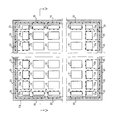
- FIG. 3 is a schematic transmission view of the EL display panel according to the present invention as viewed from the upper surface side of the panel.
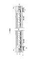
- FIG. 5 is a diagram showing a cross section of the EL display panel taken along line VV shown in FIG. 1.
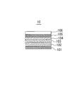
- 2 is a diagram illustrating an example of a cross-sectional structure of an EL element 10.
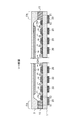
- FIG. It is a figure which shows the principle of expansion of the display area by EL display panel shown by FIG. It is a figure which shows the cross section of the EL display panel by another Example. It is a figure which shows the cross section of the EL display panel by another Example. It is a figure which shows the cross section of the EL display panel by another Example. It is a figure which shows the cross section of the EL display panel by another Example.
- a photoluminescent material is placed at a position corresponding to each of the electroluminescent elements arranged on the outermost periphery in each of the electroluminescent elements. Including a photoexcitation element.
- the visible display area in the display panel surface is expanded, and the rectangular annular non-display area formed by the adhesive layer existing on the outer peripheral portion of the display panel becomes inconspicuous.
- FIG. 1 is a schematic transmission view of an EL display panel according to the present invention as viewed from the top side of the panel
- FIG. 2 is a view showing a cross section of the EL display panel taken along the line VV shown in FIG.
- such an EL display panel has a laminated structure of a front transparent substrate 1, a planarizing layer 2 and a back substrate 3 each having a two-dimensional plane having a vertical and horizontal size equivalent to the display surface of the EL display panel. Consists of.
- One surface of the front transparent substrate 1 made of a transparent material such as glass is a display surface as an EL display panel, and a planarizing layer 2 made of a transparent material such as polyimide or an inorganic material is formed on the other surface.
- an EL element 10 that bears each pixel (including a red pixel, a blue pixel, and a green pixel) and a sealing space GA in which a partition wall 11 is to be formed are provided.
- the EL element 10 shown by a solid line
- the EL element 10 Are arranged in a matrix form in a form surrounded by the partition walls 11.
- FIG. 3 is a diagram illustrating an example of a cross-sectional structure of the EL element 10.
- the EL element 10 when the transparent electrode 101 is an anode and the back electrode 105 is a cathode is shown below.
- the EL element 10 includes a transparent electrode 101 formed on the surface of the planarizing layer 2, a hole injection layer 102 such as copper phthalocyanine (CuPc) formed on the transparent electrode 101, and a top thereof.
- CuPc copper phthalocyanine
- NPB N, N-di (naphtalence) -N, N-dipheneyl-benzidene
- the hole transport layer 103 has a function of transporting holes injected from the transparent electrode 101 to the organic light emitting layer 104.
- the hole transport layer 103 may be a single layer or a stack of two or more layers.
- the hole transport layer 103 may be formed of a plurality of materials instead of being formed by a single material, and a guest material having a high charge donating (accepting) property for a host material having a high charge transport capability. May be doped.
- the organic light emitting layer 104 is formed on the hole transport layer 103.
- red (R), green (G), and blue (B) light-emitting layers are formed in respective film formation regions by using a resistance heating vapor deposition method using a coating mask.
- red (R) an organic material that emits red light such as a styryl dye such as DCM1 (4- (dicyanomethylene) -2-methyl-6- (4′-dimethylaminostyryl) -4H-pyran) is used.
- An organic material that emits green light such as an aluminum quinolinol complex (Alq 3 ) is used as green (G).
- blue (B) an organic material emitting blue light such as a distyryl derivative or a triazole derivative is used. It should be noted that other materials such as a host-guest layer structure may be used, and the light emitting material may be a material using a fluorescent light emitting material or a phosphorescent light emitting material.
- the electron transport layer 105 formed on the organic light emitting layer 104 is formed using various materials such as an aluminum quinolinol complex (Alq 3 ) by various film forming methods such as resistance heating vapor deposition.
- the electron transport layer 105 has a function of transporting electrons injected from the back electrode 106 functioning as a cathode to the organic light emitting layer 104.
- the electron transport layer 105 may have a multilayer structure in which only one layer is stacked or two or more layers are stacked.
- the electron transport layer 105 may be formed of a plurality of materials instead of being formed using a single material, and a guest material having a high charge donating (accepting) property for a host material having a high charge transport capability. It may be formed by doping.
- the back electrode 106 is patterned in a stripe shape along a direction orthogonal to the pattern of the transparent electrode 101, for example.
- a material having a work function lower than that of the anode is used so as to have an electron injection function.
- ITO indium gallium
- Al aluminum
- Mg—Ag magnesium alloy
- Al since Al has a low electron injection capability, it is preferable to provide an electron injection layer such as LiF between Al and the electron transport layer.
- Each of the transparent electrode 101 and the back electrode 105 is connected to a lead terminal (not shown) exposed to the outside.
- the lead terminal is made of a low-resistance metal such as Al, Cr, or Ag, an alloy thereof, or a laminate.
- a desiccant 14 is attached to one surface of the back substrate 3 in the sealing space GA as described above to prevent moisture in the sealing space GA. Further, an adhesive layer 15 is formed between the end portion of the back substrate 3 and the end portion of the planarizing layer 2 to join the two and seal the sealing space GA. Due to the adhesive layer 15, a rectangular annular sealing area FA as shown by the oblique lines in FIG. 1 exists on the outer periphery of the EL display panel.
- the desiccant 14 is, for example, a physical adsorption type desiccant such as zeolite, silica gel, carbon or carbon nanotube, a chemisorption type desiccant such as alkali metal oxide, metal halide or chlorine peroxide, an organometallic complex in toluene, It consists of a desiccant dissolved in a petroleum solvent such as xylene and an aliphatic organic solvent, a desiccant obtained by dispersing desiccant particles in a binder such as polyethylene, polyisoprene, and polyvinyl cinnaate having transparency.
- a physical adsorption type desiccant such as zeolite, silica gel, carbon or carbon nanotube
- a chemisorption type desiccant such as alkali metal oxide, metal halide or chlorine peroxide
- an organometallic complex in toluene It consists of a desiccant dissolved in a petroleum solvent
- the adhesive 15 is made of a thermosetting type, chemical curable type (two-component mixture), or light (ultraviolet) curable material such as an acrylic resin, an epoxy resin, a polyester, or a polyolefin.
- a thermosetting type such as an acrylic resin, an epoxy resin, a polyester, or a polyolefin.
- light (ultraviolet) curable material such as an acrylic resin, an epoxy resin, a polyester, or a polyolefin.
- an ultraviolet curable epoxy resin adhesive that does not require heat treatment and has high immediate curing properties.
- glass may be used as the adhesive 15.
- the sealing space GA having the above-described sealing recess may be formed according to the hermetic sealing method, or a filler such as resin or silicone oil is sealed in the sealing space GA.
- a filler such as resin or silicone oil
- a solid sealing method in which a resin film and a metal foil are sealed, or a film sealing method in which the EL element 10 is sealed with a barrier film or the like may be employed.
- each EL excitation element 20 is on the outermost periphery of the EL element 10 on the surface of the front transparent substrate 1 (the surface different from the display surface), that is, the EL display panel. It is formed at a position corresponding to each EL element 10a disposed at a position closest to the end.
- each EL excitation element 20 is disposed at a position corresponding to each EL element 10a at a position closer to the end of the EL display panel than this EL element 10a.
- each EL excitation element 20 has a sealing region FA on the vertical axis (shown by a broken line) including one end V1 with respect to the surface of the EL excitation element 20,
- the element width (V1 to V2) is such that the light emitting surface of the EL element 10a exists on the vertical axis (shown by a broken line) including the other end V2.
- the EL excitation element 20 is sealed by the adhesive layer 15 in a region facing one surface (the surface not in contact with the front transparent substrate 1).
- the width is such that a part (or all) of the FA and a part (or all) of the light emitting surface of the EL element 10a are included.
- a driving IC or the like for driving light emission / non-light emission of the extraction terminal or EL element may be formed. According to the present invention, since the sealing area FA can be formed widely, there is an effect that the degree of freedom in designing the EL display panel is increased.
- the EL element 10 formed on the transparent substrate 1 can be applied to either a single element or an element having a structure arranged in an array.
- the light emitting / non-light emitting driving method of the EL element 10 may be either a passive driving method in which the transparent electrode 101 and the back electrode 106 are formed in an XY matrix, or an active driving method using TFTs.
- the photoexcitation layer is formed by dispersing a so-called photoluminescence (hereinafter referred to as PL) material that is excited when receiving light in a base material such as a polymer.
- PL photoluminescence
- an excitation light emitting dye material having an absorption peak in the region of 250 to 780 nm and an emission wavelength that is longer than the excited absorption peak is used.
- a band gap engineered inorganic compound composed of Y 2 O 2 S: Eu, Gd, ZnS: Cu, Al, BaMgAl 10 O 17 : Eu, SiAlON phosphor, etc., CdSe / ZnS nanocrystals (Quantum Dot Nanomaterials), p -Phenyl compounds such as Terphenyl, p-Quaterphenyl, and dye (including laser dye) organic compounds such as Coumarin derivatives and Rhodamine derivatives.
- a base material such as a polymer, a material having transparency such as an acrylic material, an epoxy material, or PMMA is preferable.
- the concentration when the PL excitation material is dispersed in the base material is preferably a concentration range in which concentration quenching of the PL excitation material does not occur.
- a photoexcitation layer is formed on the surface of the front transparent substrate 1 through the process as described above, and then the planarization layer 2 is formed on the front transparent substrate 1 so as to cover the photoexcitation layer in order to eliminate a step due to the photoexcitation layer. It forms.
- the photoexcitation layer is excited and emits light when its surface receives light emitted from the EL element 10, particularly the EL element 10 a disposed at a position closest to the end of the EL display panel. That is, first, on the surface of the photoexcitation layer, PL excited particles existing in a region directly receiving the irradiation light from the EL element 10a emit light. Then, by the emission of the PL excited particles, each of the PL excited particles existing in a region not directly receiving the irradiation light from the EL element 10a is also excited in a chain and emits light. Thereby, as shown in FIG. 4, it becomes possible to make irradiation light from the EL element 10a reach the sealing area FA.
- the visible display area can be extended to the extreme end of the EL display panel regardless of the width W of the sealing area FA as shown in FIG.
- the width W of the sealing area FA is increased in order to increase the hermetic reliability of the sealing space GA in which the plurality of EL elements 10 are formed
- the non-display area due to the sealing area FA is made inconspicuous. Will be able to.
- a plurality of photoexcitation layers are provided on each of the EL elements 10a arranged on the outermost side among the EL elements 10 arranged in a matrix as shown in FIG. Although it is provided only at the corresponding position, it may be provided at a position corresponding to each of all the EL elements 10 as shown in FIG.
- a plurality of photoexcitation layers are formed on the surface of the front transparent substrate 1 that is different from the display surface, but these photoexcitation layers ( Each of the EL excitation elements 20) may be formed on the display surface side of the front transparent substrate 1 as shown in FIG. 6 or FIG.
- the planarization layer 2 is unnecessary, and thus a structure in which this is omitted is adopted.
Landscapes
- Electroluminescent Light Sources (AREA)
- Devices For Indicating Variable Information By Combining Individual Elements (AREA)
Abstract
【課題】EL素子の材質劣化を生じさせることなく、パネル面内の最外周に存在する非表示領域を目立たなくすることが可能なEL表示パネルを提供することを目的とする。 【解決手段】複数のエレクトロルミネッセンス素子を備えたEL表示パネルの前面透明基板の面上において、エレクトロルミネッセンス素子各々の内で最外周に配置されているエレクトロルミネッセンス素子の各々に対応した位置に、フォトルミネセンス材料を含む光励起層を設ける。
Description
入力映像信号に対応した画像を表示する表示パネルに関し、特にエレクトロルミネッセンス(以下、ELと称する)表示パネルに関する。
現在、薄型の自発光型の表示パネルとして、有機材料を発光層として用いたEL表示パネルが製品化されている。
又、近年、このようなEL表示パネルの複数をマトリクス状に配列して1つの表示パネルを構築するようにした技術が提案されている(例えば、特許文献1の図1及び図2参照)。
かかる表示パネルにおいて、各EL表示パネル(2a~2d)は、前面ガラス基板(8a,8b)と背面ガラス基板(10a,10b)との間に、夫々画素を担う複数の発光部(7a,7b)が形成された構成となっている。更に、各発光部が外気と触れることによって生じる材質劣化を抑える為に、各EL表示パネルの端部(90a、90b)には、接着剤が充填されてなる封止領域が存在する。この際、封止領域では発光部を形成させることができないので、EL表示パネルのパネル面内には、発光部によって画像表示が為される表示領域の周囲に、表示が為されない矩形環状の非表示領域が存在することになる。よって、このようなEL表示パネルの複数をマトリクス状に配列してなる表示画面を眺めると、EL表示パネル同士の境界部において、非表示領域による格子状の暗線が視覚されてしまう。尚、かかる暗線を目立たなくすべく非表示領域(封止領域)の幅を狭めると、発行部に対する気密信頼性が低下して材質劣化の虞が生じてしまう。
特開2003-098980号公報
本発明は、EL素子の材質劣化を生じさせることなく、パネル面内の最外周に存在する非表示領域を目立たなくすることが可能なEL表示パネルを提供することを目的とするものである。
本発明の第1の特徴によるEL表示パネルは、一方の面が表示面を担う前面透明基板と、背面基板と、前記前面透明基板及び前記背面基板間の封止空間内に形成されている複数のエレクトロルミネッセンス素子と、を備えたEL表示パネルであって、前記前面透明基板の他方の面上において、前記エレクトロルミネッセンス素子各々の内で最外周に配置されているエレクトロルミネッセンス素子の各々に対応した位置にフォトルミネセンス材料を含む光励起素子が形成されている。
本発明の第2の特徴によるEL表示パネルは、一方の面が表示面を担う前面透明基板と、背面基板と、前記前面透明基板及び前記背面基板間の封止空間内に形成されている複数のエレクトロルミネッセンス素子と、を備えたEL表示パネルであって、前記前面透明基板の前記表示面上において、前記エレクトロルミネッセンス素子各々の内で最外周に配置されているエレクトロルミネッセンス素子の各々に対応した位置にフォトルミネセンス材料を含む光励起素子が形成されている。
複数のエレクトロルミネッセンス素子を備えたEL表示パネルの前面透明基板の面上において、エレクトロルミネッセンス素子各々の内で最外周に配置されているエレクトロルミネッセンス素子の各々に対応した位置に、フォトルミネセンス材料を含む光励起素子を設ける。これにより、表示パネル面内において視覚される表示領域が拡張されるので、表示パネルの外周部に存在する接着層による矩形環状の非表示領域が目立たなくなる。
図1は、本発明によるEL表示パネルをパネル上面側から眺めた概略透過図であり、図2は、図1に示すV-V線におけるEL表示パネルの断面を示す図である。
図2に示すように、かかるEL表示パネルは、夫々が、このEL表示パネルの表示面と同等な縦横サイズの2次元平面を有する前面透明基板1、平坦化層2及び背面基板3による積層構造からなる。ガラス等の透明材料からなる前面透明基板1の一方の面がEL表示パネルとしての表示面となり、その他方の面には、ポリイミド或いは無機材料等の透明材料からなる平坦化層2が形成されている。平坦化層2及び背面基板3間には、各画素(赤色画素、青色画素、緑色画素を含む)を担うEL素子10及び隔壁11が形成されるべき封止空間GAが設けられている。かかる封止空間GA内における、平坦化層2の一方の面(前面透明基板1とは接触していない方の面)上において、図1に示すように、EL素子10(実線にて示す)の各々が隔壁11に囲まれた形態にてマトリクス状に配列して形成されているのである。
図3は、EL素子10の断面構造の一例を示す図である。透明電極101を陽極として、背面電極105を陰極とした場合のEL素子10の例を以下に示す。図3に示すように、EL素子10は、平坦化層2の面上に形成された透明電極101、透明電極101上に銅フタロシアニン(CuPc)等の正孔注入層102を形成し、その上に、例えば、NPB(N,N-di(naphtalence)-N,N-dipheneyl-benzidene)を正孔輸送層103として成膜する。この正孔輸送層103は、透明電極101から注入される正孔を有機発光層104に輸送する機能を有する。この正孔輸送層103は、1層だけ積層したものでも2層以上積層したものであってもよい。また正孔輸送層103は、単一の材料による成膜ではなく、複数の材料により一つの層を形成しても良く、電荷輸送能力の高いホスト材料に電荷供与(受容)性の高いゲスト材料をドーピングしてもよい。
次に、正孔輸送層103の上に有機発光層104を成膜する。一例としては、抵抗加熱蒸着法により、赤(R)、緑(G)、青(B)の発光層を、塗分け用マスクを利用してそれぞれの成膜領域に成膜する。赤(R)としてDCM1(4-(ジシアノメチレン)-2-メチル-6-(4’-ジメチルアミノスチリル)-4H-ピラン)等のスチリル色素等の赤色を発光する有機材料を用いる。緑(G)としてアルミキノリノール錯体(Alq3) 等の緑色を発光する有機材料を用いる。青(B)としてジスチリル誘導体、トリアゾール誘導体等の青色を発光する有機材料を用いる。尚、他の材料、例えばホスト-ゲスト系の層構成でも良く、その発光材料としても、蛍光発光材料或いはりん光発光材料を用いたものであってもよい。
次に、正孔輸送層103の上に有機発光層104を成膜する。一例としては、抵抗加熱蒸着法により、赤(R)、緑(G)、青(B)の発光層を、塗分け用マスクを利用してそれぞれの成膜領域に成膜する。赤(R)としてDCM1(4-(ジシアノメチレン)-2-メチル-6-(4’-ジメチルアミノスチリル)-4H-ピラン)等のスチリル色素等の赤色を発光する有機材料を用いる。緑(G)としてアルミキノリノール錯体(Alq3) 等の緑色を発光する有機材料を用いる。青(B)としてジスチリル誘導体、トリアゾール誘導体等の青色を発光する有機材料を用いる。尚、他の材料、例えばホスト-ゲスト系の層構成でも良く、その発光材料としても、蛍光発光材料或いはりん光発光材料を用いたものであってもよい。
有機発光層104の上に成膜される電子輸送層105は、抵抗加熱蒸着法等の各種成膜方法により、例えばアルミキノリノール錯体(Alq3 )等の各種材料を用いて成膜する。電子輸送層105は、陰極として機能する背面電極106から注入される電子を有機発光層104に輸送する機能を有する。この電子輸送層105は、1層だけ積層したものでも2層以上積層した多層構造を有してもよい。また、電子輸送層105は、単一の材料による成膜ではなく、複数の材料により一つの層を形成しても良く、電荷輸送能力の高いホスト材料に電荷供与(受容)性の高いゲスト材料をドーピングして形成してもよい。
背面電極106は、例えば、透明電極101のパターンと直交する方向に沿ってストライプ状にパターニングされる。背面106は、陰極として機能する場合には、電子注入機能を有するように、陽極より仕事関数の低い材料を用いる。例えば、陽極としてITOを用いた場合には、アルミニウム(Al)やマグネシウム合金(Mg-Ag)を利用するのが好ましい。但し、Alは電子注入能力が低いためにAlと電子輸送層との間にLiFのような電子注入層を設けることが好ましい。
尚、透明電極101及び背面電極105の各々は、外部に露出している引出端子(図示せず)に接続されている。引出端子は、低抵抗のAl、Cr、Ag等の金属や、その合金或いは積層体からなる。
尚、上記の如き封止空間GA内における背面基板3の一方の面には、この封止空間GAの湿気を防ぐ為の乾燥材14が貼り付けられている。又、背面基板3の端部と平坦化層2の端部との間には、両者を接合し且つ封止空間GAを密封する為の接着層15が形成されている。かかる接着層15により、EL表示パネルの外周には、図1の斜線にて示されるが如き矩形環状の封止領域FAが存在する。
乾燥剤14は、例えばゼオライト、シリカゲル、カーボン、カーボンナノチューブ等の物理吸着タイプの乾燥剤、アルカリ金属酸化物、金属ハロゲン化物、過酸化塩素等の化学吸着タイプの乾燥剤、有機金属錯体をトルエン、キシレン、脂肪族有機溶剤等の石油系溶媒に溶解した乾燥剤、乾燥剤粒子を透明性を有するポリエチレン、ポリイソプレン、ポリビニルシンナエート等のバインダに分散させた乾燥剤等からなる。
接着剤15は、熱硬化型、化学硬化型(2液混合)、光(紫外線)硬化型の材料、例えばアクリル樹脂、エポキシ樹脂、ポリエステル、ポリオレフィン等からなる。特に、加熱処理を要さず即硬化性の高い紫外線硬化型のエポキシ樹脂製接着剤を用いるのか好ましい。尚、接着剤15としては、ガラスを用いるようにしても良い。
また、気密封止法に従って上記のような封止用凹部を有する封止空間GAを形成するようにしても良く、或いは、封止空間GA内に例えば樹脂やシリコーンオイル等の充填剤を封入したもの、例えば樹脂フィルムと金属箔で封止した固体封止法、バリア膜等でEL素子10を封止する膜封止法を採用してもよい。
ここで、平坦化層2内には、光励起層としてのEL励起素子20(図1の一点鎖線にて囲まれた部分)が複数個、形成されている。平坦化層2は、透光性と絶縁性を有する材料が好ましく、ポリイミド、アクリル、SiO2等で形成されている。
各EL励起素子20は、前面透明基板1の面(表示面とは異なる方の面)上において、図1又は図2に示す如く、EL素子10各々の内で最外周、つまりEL表示パネルの端部に最も近い位置に配置されているEL素子10aに夫々対応した位置に形成されている。具体的には、各EL励起素子20は、各EL素子10aに対応した位置において、このEL素子10aよりもEL表示パネルの端部に近い位置に配置されている。この際、各EL励起素子20は、図2に示す如く、EL励起素子20の面に対して、その一端V1を含む垂直軸上(破線にて示す)に封止領域FAが存在すると共に、その他端V2を含む垂直軸上(破線にて示す)にEL素子10aの発光面が存在するような素子幅(V1~V2)を有する。つまり、EL励起素子20は、図1又は図2に示すように、その一方の面(前面透明基板1と接触していない方の面)に対向する領域中に、接着層15による封止領域FAの一部(又は全て)と、上記EL素子10aによる発光面の一部(又は全て)とが共に含まれるような幅を有するものである。
各EL励起素子20は、前面透明基板1の面(表示面とは異なる方の面)上において、図1又は図2に示す如く、EL素子10各々の内で最外周、つまりEL表示パネルの端部に最も近い位置に配置されているEL素子10aに夫々対応した位置に形成されている。具体的には、各EL励起素子20は、各EL素子10aに対応した位置において、このEL素子10aよりもEL表示パネルの端部に近い位置に配置されている。この際、各EL励起素子20は、図2に示す如く、EL励起素子20の面に対して、その一端V1を含む垂直軸上(破線にて示す)に封止領域FAが存在すると共に、その他端V2を含む垂直軸上(破線にて示す)にEL素子10aの発光面が存在するような素子幅(V1~V2)を有する。つまり、EL励起素子20は、図1又は図2に示すように、その一方の面(前面透明基板1と接触していない方の面)に対向する領域中に、接着層15による封止領域FAの一部(又は全て)と、上記EL素子10aによる発光面の一部(又は全て)とが共に含まれるような幅を有するものである。
ここで、封止領域FAには、前記引出端子やEL素子の発光/非発光を駆動する駆動用IC等を形成しても良い。本発明により、封止領域FAを広く形成できるためEL表示パネルの設計の自由度が広がる効果も有している。
本発明では、透明基板1上に形成するEL素子10が、単一の素子、アレイ状に配置された構造からなる素子のいずれにおいても適用することができる。また、EL素子10の発光/非発光の駆動方式も透明電極101と背面電極106をX-Yマトリックス状に形成したパッシブ駆動方式、TFTによるアクティブ駆動方式のいずれでも良い。
光励起層は、光を受けると励起するいわゆるフォトルミネセンス(以下、PLと称する)材料をポリマー等の基材中に分散させて含ませることにより形成される。
PL励起する材料としては、250~780nmの領域に吸収ピークを持ち、発光波長は励起された吸収ピークより長波長側の波長ピークが得られる励起発光色素材料を用いる。例えば、Y2O2S:Eu,Gd、ZnS:Cu,Al、BaMgAl10O17:Eu、SiAlON蛍光体等からなるバンドギャップエンジニアリングした無機化合物、CdSe/ZnSナノクリスタル(Quantum Dot Nanomaterials)、p-Terphenyl,p-Quaterphenyl等のフェニル系化合物、及び、Coumarin誘導体、Rhodamine誘導体等の色素(レーザー色素含む)系有機化合物が挙げられる。ポリマー等の基材としては、アクリル系材料、エポキシ系材料、PMMA等の透過性を有する材料が好ましい。
このような基材中に上記の如きPL励起する材料を分散形成させる為のプロセスとしては、
(1)PL励起材料及び基材を同時に蒸着してパターニング
(2)PL励起材料及び基材を含む混合液を塗布、インクジェット、印刷にてパターン形成
(3)PL励起材料を基材に分散させたフィルムをパターン形成・貼り付け、或いは転写
等の各種プロセスを採用可能である。
(1)PL励起材料及び基材を同時に蒸着してパターニング
(2)PL励起材料及び基材を含む混合液を塗布、インクジェット、印刷にてパターン形成
(3)PL励起材料を基材に分散させたフィルムをパターン形成・貼り付け、或いは転写
等の各種プロセスを採用可能である。
この際、PL励起材料を基材に分散する際の濃度は、PL励起する材料の濃度消光が生じない程度の濃度範囲が好ましい。
すなわち、上記の如きプロセスを経て前面透明基板1の面上に光励起層が形成され、その後、光励起層による段差を無くすために、光励起層を覆うように平坦化層2を前面透明基板1上に形成するのである。
光励起層は、EL素子10、特にEL表示パネルの端部に最も近い位置に配置されているEL素子10aから照射された光をその表面に受けると、励起し発光する。すなわち、先ず、光励起層の表面において、EL素子10aからの照射光を直接受けた領域に存在するPL励起粒子が発光する。そして、このPL励起粒子の発光により、EL素子10aからの照射光を直接受けていない領域に存在するPL励起粒子の各々も連鎖的に励起して発光する。これにより、図4に示すように、EL素子10aからの照射光を封止領域FA内にまで至らせることが可能となる。
従って、光励起層によれば、図4に示す如き封止領域FAの幅Wに拘わらず、視覚される表示領域をEL表示パネルの最端部にまで広げることが可能になるのである。これにより、複数のEL素子10が形成されている封止空間GAの気密信頼性を高めるべく封止領域FAの幅Wを広げても、この封止領域FAによる非表示領域を目立たなくすることができるようになる。
尚、上記実施例では、複数の光励起層(EL励起素子20)を、図1に示す如くマトリクス状に配列されているEL素子10の内で最も外側に配置されているEL素子10aの各々に対応した位置にだけ設けるようにしているが、図5に示すように、全てのEL素子10の各々に対応した位置に、夫々設けるようにしても良い。
又、図2又は図5に示す一例では、前面透明基板1における2つの面の内で表示面とは異なる方の面側に複数の光励起層を形成するようにしているが、これら光励起層(EL励起素子20)の各々を、図6又は図7に示す如く、前面透明基板1の表示面側に形成するようにしても良い。この際、図6又は図7に示すように、平坦化層2は不要となるのでこれを省いた構造を採用する。
1 前面透明基板
2 平坦化層
3 背面基板
10 EL素子
14 乾燥材
15 接着層
20 EL励起素子
2 平坦化層
3 背面基板
10 EL素子
14 乾燥材
15 接着層
20 EL励起素子
Claims (8)
- 一方の面が表示面を担う前面透明基板と、背面基板と、前記前面透明基板及び前記背面基板間の封止空間内に形成されている複数のエレクトロルミネッセンス素子と、を備えたEL表示パネルであって、
前記前面透明基板の他方の面上において、前記エレクトロルミネッセンス素子各々の内で最外周に配置されているエレクトロルミネッセンス素子の各々に対応した位置にフォトルミネセンス材料を含む光励起層が形成されていることを特徴とするEL表示パネル。 - 前記前面透明基板の他方の面上には前記光励起層を含んだ平坦化層が形成されており、
前記封止空間内における前記平坦化層の面上に前記エレクトロルミネッセンス素子の各々が形成されていることを特徴とする請求項1記載のEL表示パネル。 - 前記平坦化層及び前記背面基板各々の端部同士を接合する接着層を備え、
前記光励起層は、この光励起層の面に対して当該光励起層の一端を含む垂直軸上に前記接着層が存在すると共に、前記光励起層の面に対して当該光励起層の他端を含む垂直軸上に前記最外周に配置されているエレクトロルミネッセンス素子が存在する幅を有することを特徴とする請求項2記載のEL表示パネル。 - 前記平坦化層内における前記前面透明基板の他方の面上には、前記最外周に配置されているエレクトロルミネッセンス素子よりも内側に配置されているエレクトロルミネッセンス素子各々に対応した位置にもフォトルミネセンス材料を含む光励起層が形成されていることを特徴とする請求項1又は2に記載のEL表示パネル。
- 一方の面が表示面を担う前面透明基板と、背面基板と、前記前面透明基板及び前記背面基板間の封止空間内に形成されている複数のエレクトロルミネッセンス素子と、を備えたEL表示パネルであって、
前記前面透明基板の前記表示面上において、前記エレクトロルミネッセンス素子各々の内で最外周に配置されているエレクトロルミネッセンス素子の各々に対応した位置にフォトルミネセンス材料を含む光励起層が形成されていることを特徴とするEL表示パネル。 - 前記前面透明基板の他方の面上に前記エレクトロルミネッセンス素子の各々が形成されていることを特徴とする請求項5記載のEL表示パネル。
- 前記前面透明基板及び前記背面基板各々の端部同士を接合する接着層を備え、
前記光励起層は、この光励起層の面に対して当該光励起層の一端を含む垂直軸上に前記接着層が存在すると共に、前記光励起層の面に対して当該光励起層の他端を含む垂直軸上に前記最外周に配置されているエレクトロルミネッセンス素子が存在する幅を有することを特徴とする請求項6記載のEL表示パネル。 - 前記前面透明基板の前記表示面上には、前記最外周に配置されているエレクトロルミネッセンス素子よりも内側に配置されているエレクトロルミネッセンス素子各々に対応した位置にもフォトルミネセンス材料を含む光励起層が形成されていることを特徴とする請求項5又は6に記載のEL表示パネル。
Priority Applications (2)
| Application Number | Priority Date | Filing Date | Title |
|---|---|---|---|
| US13/203,148 US20120007500A1 (en) | 2009-02-25 | 2009-02-25 | Electroluminescent Panel |
| PCT/JP2009/053439 WO2010097917A1 (ja) | 2009-02-25 | 2009-02-25 | El表示パネル |
Applications Claiming Priority (1)
| Application Number | Priority Date | Filing Date | Title |
|---|---|---|---|
| PCT/JP2009/053439 WO2010097917A1 (ja) | 2009-02-25 | 2009-02-25 | El表示パネル |
Publications (1)
| Publication Number | Publication Date |
|---|---|
| WO2010097917A1 true WO2010097917A1 (ja) | 2010-09-02 |
Family
ID=42665144
Family Applications (1)
| Application Number | Title | Priority Date | Filing Date |
|---|---|---|---|
| PCT/JP2009/053439 Ceased WO2010097917A1 (ja) | 2009-02-25 | 2009-02-25 | El表示パネル |
Country Status (2)
| Country | Link |
|---|---|
| US (1) | US20120007500A1 (ja) |
| WO (1) | WO2010097917A1 (ja) |
Citations (3)
| Publication number | Priority date | Publication date | Assignee | Title |
|---|---|---|---|---|
| JP2003249364A (ja) * | 2002-02-22 | 2003-09-05 | Dainippon Printing Co Ltd | 有機エレクトロルミネッセント画像表示装置およびその製造方法 |
| JP2004022517A (ja) * | 2002-06-20 | 2004-01-22 | Fuji Electric Holdings Co Ltd | 有機el表示装置および有機el表示装置の製造方法 |
| JP2006030548A (ja) * | 2004-07-15 | 2006-02-02 | Nec Corp | 光学基板、発光素子、表示装置およびそれらの製造方法 |
Family Cites Families (1)
| Publication number | Priority date | Publication date | Assignee | Title |
|---|---|---|---|---|
| JP3650101B2 (ja) * | 2003-02-04 | 2005-05-18 | 三洋電機株式会社 | 有機エレクトロルミネッセンス装置およびその製造方法 |
-
2009
- 2009-02-25 WO PCT/JP2009/053439 patent/WO2010097917A1/ja not_active Ceased
- 2009-02-25 US US13/203,148 patent/US20120007500A1/en not_active Abandoned
Patent Citations (3)
| Publication number | Priority date | Publication date | Assignee | Title |
|---|---|---|---|---|
| JP2003249364A (ja) * | 2002-02-22 | 2003-09-05 | Dainippon Printing Co Ltd | 有機エレクトロルミネッセント画像表示装置およびその製造方法 |
| JP2004022517A (ja) * | 2002-06-20 | 2004-01-22 | Fuji Electric Holdings Co Ltd | 有機el表示装置および有機el表示装置の製造方法 |
| JP2006030548A (ja) * | 2004-07-15 | 2006-02-02 | Nec Corp | 光学基板、発光素子、表示装置およびそれらの製造方法 |
Also Published As
| Publication number | Publication date |
|---|---|
| US20120007500A1 (en) | 2012-01-12 |
Similar Documents
| Publication | Publication Date | Title |
|---|---|---|
| CN105161513B (zh) | Oled显示装置及其制造方法、彩膜基板及其制造方法 | |
| US7250721B2 (en) | Organic EL element and organic EL display panel | |
| JP5576296B2 (ja) | 有機el装置およびその製造方法 | |
| JP4186289B2 (ja) | 有機エレクトロルミネッセンス表示素子用基板の製造方法および有機エレクトロルミネッセンス表示素子の製造方法 | |
| JP6718955B2 (ja) | 有機el表示装置 | |
| CN105742320A (zh) | 具有量子点的有机发光二极管显示器 | |
| WO2012043611A1 (ja) | 有機el表示装置、及びその製造方法 | |
| JP2004281085A (ja) | フレキシブル有機elデバイスおよびフレキシブル有機elディスプレイ | |
| US7948160B2 (en) | Optical device and manufacturing method of the optical device | |
| JP2005019151A (ja) | 有機elパネル及びその製造方法 | |
| JP4986904B2 (ja) | 発光装置及びその製造方法 | |
| JP3591387B2 (ja) | 有機el素子 | |
| JP2007103164A (ja) | 自発光パネル、および自発光パネルの製造方法。 | |
| JP2004022517A (ja) | 有機el表示装置および有機el表示装置の製造方法 | |
| WO2010097917A1 (ja) | El表示パネル | |
| JP5265018B2 (ja) | 有機elパネル及びその製造方法 | |
| CN1976086B (zh) | 自发光面板及其制造方法 | |
| KR100739651B1 (ko) | 유기 전계 발광 표시장치 및 이의 제조 방법 | |
| JP2005353287A (ja) | 有機el素子及びその製造方法 | |
| JP5330655B2 (ja) | 有機el表示装置 | |
| JP2011029108A (ja) | 有機el素子 | |
| KR100522693B1 (ko) | 유기 전계 발광표시장치 | |
| KR20060081649A (ko) | 광 여기 확산물질을 이용한 풀 칼라 유기 발광 다이오드디스플레이 구조 및 제조방법 | |
| JP2005251629A (ja) | 有機elパネル及びその製造方法 | |
| KR100740134B1 (ko) | 유기 전계 발광 표시장치 및 이의 제조 방법 |
Legal Events
| Date | Code | Title | Description |
|---|---|---|---|
| 121 | Ep: the epo has been informed by wipo that ep was designated in this application |
Ref document number: 09840770 Country of ref document: EP Kind code of ref document: A1 |
|
| NENP | Non-entry into the national phase |
Ref country code: DE |
|
| WWE | Wipo information: entry into national phase |
Ref document number: 13203148 Country of ref document: US |
|
| 122 | Ep: pct application non-entry in european phase |
Ref document number: 09840770 Country of ref document: EP Kind code of ref document: A1 |
|
| NENP | Non-entry into the national phase |
Ref country code: JP |