WO2010097905A1 - パッケージの製造方法及び圧電振動子、発振器、電子機器、並びに電波時計 - Google Patents
パッケージの製造方法及び圧電振動子、発振器、電子機器、並びに電波時計 Download PDFInfo
- Publication number
- WO2010097905A1 WO2010097905A1 PCT/JP2009/053334 JP2009053334W WO2010097905A1 WO 2010097905 A1 WO2010097905 A1 WO 2010097905A1 JP 2009053334 W JP2009053334 W JP 2009053334W WO 2010097905 A1 WO2010097905 A1 WO 2010097905A1
- Authority
- WO
- WIPO (PCT)
- Prior art keywords
- hole
- glass frit
- electrode
- substrate
- manufacturing
- Prior art date
- Legal status (The legal status is an assumption and is not a legal conclusion. Google has not performed a legal analysis and makes no representation as to the accuracy of the status listed.)
- Ceased
Links
Images











Classifications
-
- H—ELECTRICITY
- H03—ELECTRONIC CIRCUITRY
- H03H—IMPEDANCE NETWORKS, e.g. RESONANT CIRCUITS; RESONATORS
- H03H9/00—Networks comprising electromechanical or electro-acoustic elements; Electromechanical resonators
- H03H9/02—Details
- H03H9/05—Holders or supports
- H03H9/10—Mounting in enclosures
- H03H9/1007—Mounting in enclosures for bulk acoustic wave [BAW] devices
- H03H9/1014—Mounting in enclosures for bulk acoustic wave [BAW] devices the enclosure being defined by a frame built on a substrate and a cap, the frame having no mechanical contact with the BAW device
- H03H9/1021—Mounting in enclosures for bulk acoustic wave [BAW] devices the enclosure being defined by a frame built on a substrate and a cap, the frame having no mechanical contact with the BAW device the BAW device being of the cantilever type
-
- H—ELECTRICITY
- H03—ELECTRONIC CIRCUITRY
- H03H—IMPEDANCE NETWORKS, e.g. RESONANT CIRCUITS; RESONATORS
- H03H9/00—Networks comprising electromechanical or electro-acoustic elements; Electromechanical resonators
- H03H9/15—Constructional features of resonators consisting of piezoelectric or electrostrictive material
- H03H9/21—Crystal tuning forks
-
- Y—GENERAL TAGGING OF NEW TECHNOLOGICAL DEVELOPMENTS; GENERAL TAGGING OF CROSS-SECTIONAL TECHNOLOGIES SPANNING OVER SEVERAL SECTIONS OF THE IPC; TECHNICAL SUBJECTS COVERED BY FORMER USPC CROSS-REFERENCE ART COLLECTIONS [XRACs] AND DIGESTS
- Y10—TECHNICAL SUBJECTS COVERED BY FORMER USPC
- Y10T—TECHNICAL SUBJECTS COVERED BY FORMER US CLASSIFICATION
- Y10T29/00—Metal working
- Y10T29/42—Piezoelectric device making
Definitions
- the present invention relates to a package manufacturing method, a piezoelectric vibrator, an oscillator, an electronic device, and a radio timepiece.
- a piezoelectric vibrator using a crystal or the like as a timing source such as a time source or a control signal, a reference signal source, or the like is used in a mobile phone or a portable information terminal device.
- Various piezoelectric vibrators of this type are known, and one of them is a surface mount (SMD) type piezoelectric vibrator.
- SMD surface mount
- As this type of piezoelectric vibrator for example, a base substrate (first substrate) and a lid substrate (second substrate) bonded to each other, a cavity formed between both substrates, and hermetically sealed in the cavity And a piezoelectric vibrating piece (electronic component) housed in a state.
- This type of piezoelectric vibrator has a two-layer structure in which a base substrate and a lid substrate are directly bonded, and a piezoelectric vibrating piece is accommodated in a cavity formed between the two substrates.
- a piezoelectric vibrating piece and an external electrode formed on the base substrate are made conductive by using a conductive member formed so as to penetrate the base substrate.
- Piezoelectric vibrators are known (see, for example, Patent Document 1 and Patent Document 2).
- the piezoelectric vibrator 200 includes a base substrate 201 and a lid substrate 202 which are anodically bonded to each other via a bonding film 207, and a cavity C formed between the substrates 201 and 202. And a piezoelectric vibrating piece 203 sealed in a container.
- the piezoelectric vibrating piece 203 is, for example, a tuning fork type vibrating piece, and is mounted on the upper surface of the base substrate 201 in the cavity C via the conductive adhesive E.
- the base substrate 201 and the lid substrate 202 are insulating substrates made of, for example, ceramic or glass.
- a through hole 204 penetrating the substrate 201 is formed in the base substrate 201 of both the substrates 201 and 202.
- a conductive member 205 is embedded in the through hole 204 so as to close the through hole 204.
- the conductive member 205 is electrically connected to the external electrode 206 formed on the lower surface of the base substrate 201 and is electrically connected to the piezoelectric vibrating piece 203 mounted in the cavity C.
- the conductive member 205 closes the through hole 204 to maintain airtightness in the cavity C, and electrically connects the piezoelectric vibrating piece 203 and the external electrode 206. It plays a big role.
- a method for manufacturing the conductive member 205 described above for example, a method of filling the through-hole 204 with a conductive paste (Ag paste, Au—Sn paste, etc.) in the atmosphere, and then baking and curing it is considered. It is done. However, if baking is performed after the conductive paste is filled, organic substances contained in the conductive paste disappear due to evaporation. As a result, the volume of the conductive paste after firing is reduced as compared with that before firing, so that the surface of the conductive member 205 formed of the conductive paste is dented or, in severe cases, the through hole is opened at the center. There is a risk of getting lost.
- a conductive paste Al paste, Au—Sn paste, etc.
- a method of forming a through electrode by disposing a metal pin in the through hole 204, filling a gap between the through hole 204 and the pin with a paste-like filler, and firing the paste.
- a method of forming a through electrode by disposing a metal pin in the through hole 204, filling a gap between the through hole 204 and the pin with a paste-like filler, and firing the paste.
- the through electrode By forming the through electrode in this way, the volume reduction is only in the portion of the paste material, so that the end surface of the pin is flush with the surface of the base substrate 201. Thereby, there is no gap between the external electrode 206 connected to the pin, and conduction between the through electrode and the external electrode 206 can be ensured.
- the present invention has been made in view of the above-described problems, and can maintain the airtightness in the cavity and ensure the electrical connection between the piezoelectric vibrating piece and the external electrode, thereby improving the yield. And a piezoelectric vibrator, an oscillator, an electronic device, and a radio timepiece.
- a manufacturing method of a package according to the present invention is a manufacturing method of a package in which an electronic component can be enclosed in a cavity formed between a plurality of substrates bonded to each other.
- the filler is degassed, and bubbles contained in the filler can be removed.
- no bubbles are present in the filler, and no air is present in the through holes. Therefore, when the filler is filled in the through hole, the filler can be smoothly filled in the through hole as compared with the conventional case where the filler is filled in the atmosphere. As a result, the filler can be filled in the through hole without any gap. By firing the filler in this state, the through-holes can be sealed without gaps, so that the airtightness in the cavity can be maintained in a good state.
- volume reduction and deformation hardly occur in the fired filler, so that a through electrode having a desired dimension can be provided. Therefore, the two electrodes are in close contact with each other without generating a gap between the external electrode and the through electrode. As a result, it is possible to ensure conductivity with an electrode film (for example, an external electrode) connected to the electronic component via the through electrode. Further, since the air remaining in the through hole after the filler is fired does not leak into the cavity, the package characteristics are not deteriorated. Therefore, it is possible to manufacture a small and highly reliable package while improving the yield.
- an electrode film for example, an external electrode
- a first squeegee is scanned from one end side to the other end side of the first substrate along the surface of the first substrate to fill the through hole with the filler.
- the atmospheric pressure in the second scanning step is set higher than that in the first scanning step.
- the second scanning step can prevent evaporation of components contained in the filler by increasing the pressure in the chamber as compared with the first scanning step. The increase in the viscosity of the material can be prevented and the second scanning process can be performed smoothly.
- the core part of the conductive casing having a flat base part and a core part extending in a direction orthogonal to the surface of the base part is Inserting into a through-hole, and having a housing setting step of bringing the surface of the base portion into contact with the back surface of the first substrate.
- a paste-like glass frit is used as the filler, and the glass
- the volume reduction after firing becomes only the part of the filler filled between the core material part and the through hole.
- the core member is flush with the surface of the first substrate. Therefore, it is possible to ensure conduction between the through electrode and the external electrode without generating a gap with the external electrode connected to the core member.
- the casing having the core part formed on the base part is used, the axial direction of the core part and the axial direction of the through hole can be simply performed by pushing the base part until it contacts the first substrate. Can be substantially matched. Therefore, workability at the time of the housing setting process can be improved.
- the glass frit can be filled in the through hole without any gap, so that the through hole can be sealed without any gap by firing the glass frit thereafter.
- the core part can be firmly fixed at a predetermined position. As a result, a high quality through electrode can be formed, and electrical conductivity between the electronic component and the external electrode can be ensured.
- the viscosity of the glass frit is set to 10 Pa ⁇ s or more and 200 Pa ⁇ s or less. According to this configuration, by setting the viscosity of the glass frit to 10 Pa ⁇ s or more and 200 Pa ⁇ s or less, the fluidity of the glass frit is improved, and the filler is smoothly filled into the through holes in the filling step. Can do.
- the scanning speed of the squeegee is set to 1 mm / sec or more and 50 mm / sec or less. Setting the scanning speed of the squeegee to less than 1 mm / sec is not preferable because the above-described desired viscosity cannot be obtained and the glass frit may not enter the through hole smoothly. On the other hand, if the scanning speed of the squeegee is faster than 10 mm / sec, it is not preferable because the glass frit hardly enters the through hole.
- the glass frit can be set to the above-described desired viscosity, thereby improving the flowability of the glass frit, In the first scanning step, the filler can be smoothly filled into the through hole.
- the linear pressure acting on the glass frit from the tip of each squeegee is set to 1 mg / mm or more and 1000 mg / mm or less. According to this configuration, if the linear pressure acting on the glass frit from the squeegee is set to less than 1 mm / sec, the above-mentioned desired viscosity cannot be obtained, and the glass frit may not smoothly enter the through hole. This is not preferable. On the other hand, if the pressing force is set larger than 1000 mg / mm, it is not preferable because the first substrate is overloaded.
- the glass frit can be set to the desired viscosity described above. And the filling material can be smoothly filled in the through hole in the first scanning step.
- the piezoelectric vibrator according to the present invention is manufactured by the package manufacturing method of the present invention. According to this configuration, since the piezoelectric vibrator is manufactured by the package manufacturing method of the present invention, a small and highly reliable piezoelectric vibrator can be provided.
- the oscillator according to the present invention is characterized in that the piezoelectric vibrator of the present invention is electrically connected to an integrated circuit as an oscillator.
- the electronic device is characterized in that the piezoelectric vibrator of the present invention is electrically connected to a time measuring unit.
- the radio timepiece according to the present invention is characterized in that the piezoelectric vibrator of the present invention is electrically connected to a filter portion.
- the oscillator, electronic device, and radio timepiece according to the present invention include the above-described piezoelectric vibrator, a small and highly reliable product can be provided.
- the filler can be filled in the through hole without any gap.
- the through-holes can be sealed without gaps, so that the airtightness in the cavity can be maintained in a good state. Further, volume reduction and deformation hardly occur in the fired filler, so that a through electrode having a desired dimension can be provided. Therefore, the two electrodes are in close contact with each other without generating a gap between the external electrode and the through electrode. As a result, it is possible to ensure conductivity with an electrode film (for example, an external electrode) connected to the electronic component via the through electrode.
- an electrode film for example, an external electrode
- the piezoelectric vibrator according to the present invention since it is a piezoelectric vibrator manufactured by the method for manufacturing a package of the present invention, a small and highly reliable piezoelectric vibrator can be provided. Since the oscillator, electronic device, and radio timepiece according to the present invention include the above-described piezoelectric vibrator, a small and highly reliable product can be provided.
- FIG. 1 is an external perspective view showing an embodiment of a piezoelectric vibrator according to the present invention.
- FIG. 2 is an internal configuration diagram of the piezoelectric vibrator shown in FIG. 1, and is a view of a piezoelectric vibrating piece viewed from above with a lid substrate removed.
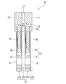
- FIG. 3 is a sectional view of the piezoelectric vibrator taken along line AA shown in FIG.
- FIG. 2 is an exploded perspective view of the piezoelectric vibrator shown in FIG. 1.
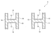
- FIG. 2 is a top view of a piezoelectric vibrating piece constituting the piezoelectric vibrator shown in FIG. 1.
- FIG. 6 is a bottom view of the piezoelectric vibrating piece shown in FIG. 5.
- FIG. 5 is an internal configuration diagram of the piezoelectric vibrator shown in FIG. 1, and is a view of a piezoelectric vibrating piece viewed from above with a lid substrate removed.
- FIG. 3 is a sectional view of the piezoelectric vibrator taken
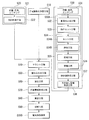
- FIG. 6 is a cross-sectional view taken along line BB shown in FIG. It is a perspective view of the cylinder which comprises the penetration electrode shown in FIG. It is a flowchart which shows the flow at the time of manufacturing the piezoelectric vibrator shown in FIG.
- FIG. 10 is a diagram illustrating a process for manufacturing a piezoelectric vibrator according to the flowchart illustrated in FIG. 9, and is a diagram illustrating a state in which a pair of through holes are formed in a base substrate wafer that is a base substrate. It is sectional drawing which follows the DD line
- FIG. 10 is a diagram illustrating a step in manufacturing the piezoelectric vibrator according to the flowchart illustrated in FIG.
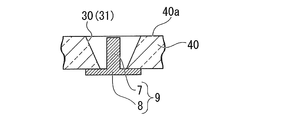
- FIG. 9 is a diagram illustrating a state in which a casing is disposed in the through hole. It is a figure which shows one process at the time of manufacturing a piezoelectric vibrator along the flowchart shown in FIG. 9, Comprising: It is a figure which shows the state filled with glass frit. It is a figure which shows one process at the time of manufacturing a piezoelectric vibrator along the flowchart shown in FIG. 9, Comprising: It is a figure which shows the state filled with the glass frit. It is a figure which shows one process at the time of manufacturing a piezoelectric vibrator along the flowchart shown in FIG. 9, Comprising: It is a figure which shows the state which removes an excess glass frit.
- FIG. 10 is a diagram illustrating a step in manufacturing the piezoelectric vibrator according to the flowchart illustrated in FIG. 9, and is a diagram illustrating a state in which a base portion of the housing is polished.
- FIG. 10 is a diagram illustrating a process for manufacturing a piezoelectric vibrator according to the flowchart illustrated in FIG.
- FIG. 1 is an external perspective view of a piezoelectric vibrator according to the present invention.
- FIG. 2 is an internal configuration diagram of the piezoelectric vibrator, and shows a piezoelectric vibrating piece viewed from above with a lid substrate removed.
- FIG. 3 is a cross-sectional view of the piezoelectric vibrator taken along line AA shown in FIG. 2, and
- FIG. 4 is an exploded perspective view of the piezoelectric vibrator.
- the piezoelectric vibrator 1 of the present embodiment is formed in a box shape in which a base substrate (first substrate) 2 and a lid substrate (second substrate) 3 are laminated in two layers.
- the excitation electrode 15, the extraction electrodes 19 and 20, the mount electrodes 16 and 17, and the weight metal film 21, which will be described later, are omitted for easy understanding of the drawing.
- the piezoelectric vibrating piece 4 is a tuning fork type vibrating piece formed of a piezoelectric material such as quartz, lithium tantalate, or lithium niobate, and vibrates when a predetermined voltage is applied. To do.
- the piezoelectric vibrating reed 4 includes a pair of vibrating arm portions 10 and 11 arranged in parallel, a base portion 12 that integrally fixes the base end sides of the pair of vibrating arm portions 10 and 11, and a pair of vibrating arm portions 10.
- the piezoelectric vibrating reed 4 of the present embodiment includes groove portions 18 formed along the longitudinal direction of the vibrating arm portions 10 and 11 on both main surfaces of the pair of vibrating arm portions 10 and 11.
- the groove portion 18 is formed from the base end side of the vibrating arm portions 10 and 11 to the vicinity of the middle.
- the excitation electrode 15 composed of the first excitation electrode 13 and the second excitation electrode 14 is an electrode that vibrates the pair of vibrating arm portions 10 and 11 at a predetermined resonance frequency in a direction approaching or separating from each other. It is formed by patterning on the outer surface of the vibrating arms 10 and 11 while being electrically separated from each other.
- the first excitation electrode 13 and the second excitation electrode 14 are electrically connected to the mount electrodes 16 and 17 via the extraction electrodes 19 and 20, respectively, on both main surfaces of the base portion 12.
- a weight metal film 21 for adjusting (frequency adjustment) so as to vibrate its own vibration state within a predetermined frequency range is coated on the tips of the pair of vibrating arm portions 10 and 11.
- the weight metal film 21 is divided into a coarse adjustment film 21a used when the frequency is roughly adjusted and a fine adjustment film 21b used when the frequency is finely adjusted.
- the piezoelectric vibrating reed 4 configured as described above is bump-bonded to the upper surface of the base substrate 2 using bumps B such as gold as shown in FIGS. More specifically, a pair of mount electrodes 16 and 17 are bump-bonded on two bumps B formed on routing electrodes 36 and 37 (described later) patterned on the upper surface of the base substrate 2. ing. As a result, the piezoelectric vibrating reed 4 is supported in a state where it floats from the upper surface of the base substrate 2, and the mount electrodes 16 and 17 and the routing electrodes 36 and 37 are electrically connected to each other.
- the above-described lid substrate 3 is a transparent insulating substrate made of a glass material, for example, soda-lime glass, and is formed in a plate shape as shown in FIGS.
- a rectangular recess 3 a in which the piezoelectric vibrating reed 4 is accommodated is formed on the bonding surface side to which the base substrate 2 is bonded.
- the recess 3 a is a cavity recess that becomes a cavity C that accommodates the piezoelectric vibrating reed 4 when the substrates 2 and 3 are overlapped.
- the lid substrate 3 is anodically bonded to the base substrate 2 with the recess 3a facing the base substrate 2 side.
- the base substrate 2 described above is a transparent insulating substrate made of a glass material, for example, soda-lime glass, like the lid substrate 3, and has a size that can be superimposed on the lid substrate 3 as shown in FIGS. It is formed in a plate shape.
- the base substrate 2 is formed with a pair of through holes (through holes) 30 and 31 penetrating the base substrate 2 in the thickness direction. At this time, the pair of through holes 30 and 31 are formed so as to be accommodated in the cavity C. More specifically, in the through holes 30 and 31 of the present embodiment, one through hole 30 is formed at a position corresponding to the base 12 side of the mounted piezoelectric vibrating reed 4, and the distal ends of the vibrating arm portions 10 and 11 are formed.
- the other through hole 31 is formed at a position corresponding to.
- a through hole having a tapered cross section whose diameter gradually decreases from the lower surface to the upper surface of the base substrate 2 will be described as an example.
- the present invention is not limited to this, and the base substrate 2 is straightened.
- a through hole that penetrates may be used. In any case, it only has to penetrate the base substrate 2.
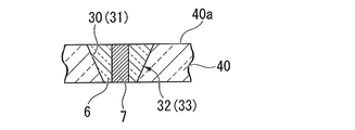
- a pair of through electrodes 32 and 33 formed so as to fill the through holes 30 and 31 are formed.
- the through electrodes 32 and 33 are formed by the cylindrical body 6 and the core member 7 that are integrally fixed to the through holes 30 and 31 by firing. 31 are completely closed to maintain the airtightness in the cavity C, and the external electrodes 38 and 39, which will be described later, and the routing electrodes 36 and 37 are electrically connected.
- FIG. 8 is a perspective view of the cylinder.
- the cylindrical body 6 is obtained by firing a pasty glass frit 6a (see FIG. 14).
- the cylindrical body 6 is formed in a cylindrical shape having both ends flat and substantially the same thickness as the base substrate 2.
- the core part 7 is distribute
- the outer shape of the cylindrical body 6 is formed in a conical shape (tapered cross section) according to the shape of the through holes 30 and 31.
- the cylindrical body 6 is fired while being embedded in the through holes 30 and 31, and is firmly fixed to the through holes 30 and 31.
- the core material portion 7 is a conductive core material formed in a cylindrical shape from a metal material, and is formed so that both ends are flat and substantially the same thickness as the thickness of the base substrate 2, similar to the cylindrical body 6. Yes. As shown in FIG. 4, when the through electrodes 32 and 33 are formed as finished products, the core material portion 7 is formed to have substantially the same thickness as the base substrate 2 as described above. However, in the manufacturing process, the length of the core member 7 is 0.02 mm shorter than the initial thickness of the base substrate 2 in the manufacturing process (later described in the description of the manufacturing method). Details.) The core portion 7 is located in the center hole 6 c of the cylindrical body 6 and is firmly fixed to the cylindrical body 6 by firing the cylindrical body 6. The through electrodes 32 and 33 are ensured to have electrical conductivity through the conductive core portion 7.
- a conductive material for example, aluminum
- a bonding film 35 for anodic bonding are paired.
- the lead-out electrodes 36 and 37 are patterned.
- the bonding film 35 is formed along the periphery of the base substrate 2 so as to surround the periphery of the recess 3 a formed in the lid substrate 3.
- the pair of lead-out electrodes 36 and 37 electrically connect one of the through electrodes 32 and 33 to the one mount electrode 16 of the piezoelectric vibrating reed 4 and the other through electrode.
- 33 and the other mount electrode 17 of the piezoelectric vibrating reed 4 are patterned so as to be electrically connected.
- Bumps B are formed on the pair of routing electrodes 36 and 37, and the piezoelectric vibrating reed 4 is mounted using the bumps B.
- one mount electrode 16 of the piezoelectric vibrating reed 4 is electrically connected to one through electrode 32 through one routing electrode 36, and the other mount electrode 17 is passed through the other routing electrode 37 to the other penetration electrode.
- the electrode 33 is electrically connected.
- a predetermined drive voltage is applied to the external electrodes 38 and 39 formed on the base substrate 2.
- a current can flow through the excitation electrode 15 including the first excitation electrode 13 and the second excitation electrode 14 of the piezoelectric vibrating reed 4, and the predetermined amount is set in a direction in which the pair of vibrating arm portions 10 and 11 are approached and separated.
- Can be vibrated at a frequency of The vibration of the pair of vibrating arm portions 10 and 11 can be used as a time source, a control signal timing source, a reference signal source, and the like.
- piezoelectric vibrator manufacturing method Next, referring to the flowchart shown in FIG. 9, a plurality of piezoelectric vibrators 1 are manufactured at a time using the base substrate wafer 40 to be the base substrate 2 and the lid substrate wafer to be the lid substrate 3. The manufacturing method will be described below.
- the piezoelectric vibrating reed manufacturing process is performed to manufacture the piezoelectric vibrating reed 4 shown in FIGS. 5 to 7 (S10).
- the resonance frequency is coarsely adjusted. This is performed by irradiating the coarse adjustment film 21a of the weight metal film 21 with laser light to evaporate a part thereof and changing the weight. Note that fine adjustment for adjusting the resonance frequency with higher accuracy is performed after mounting.
- a first wafer manufacturing process is performed in which a lid substrate wafer (not shown) to be the lid substrate 3 later is manufactured up to a state immediately before anodic bonding (S20).
- a lid substrate wafer (not shown) to be the lid substrate 3 later is manufactured up to a state immediately before anodic bonding (S20).
- a disk-shaped lid substrate wafer is formed by removing the outermost work-affected layer by etching or the like (S21).
- a recess forming step is performed for forming a plurality of cavity recesses 3a in the matrix direction by etching or the like on the bonding surface of the lid substrate wafer (S22). At this point, the first wafer manufacturing process is completed.
- a second wafer manufacturing process is performed in which a base substrate wafer 40 (see FIG. 10), which will later become the base substrate 2, is manufactured up to the state immediately before anodic bonding (see FIG. 10).
- S30 First, after polishing and washing soda-lime glass to a predetermined thickness, a disk-shaped base substrate wafer 40 is formed by removing the outermost work-affected layer by etching or the like (S31).
- S31 polishing and washing soda-lime glass to a predetermined thickness
- a through electrode forming step for forming a plurality of pairs of through electrodes 32 and 33 on the base substrate wafer 40 is performed (S30A).
- FIG. 10 is a process diagram showing a through electrode forming process, and is a perspective view of a base substrate wafer.
- FIG. 11 is a cross-sectional view taken along the line DD in FIG.
- the through electrode forming step (S30A) will be described in detail.
- a through hole forming step (S 32) for forming a plurality of pairs of through holes 30 and 31 penetrating the base substrate wafer 40 is performed.
- the broken line M shown in FIG. 10 has shown the cutting line cut
- through holes 30 and 31 having a tapered cross section whose diameter gradually decreases from the lower surface to the upper surface of the base substrate wafer 40 can be formed. Further, when the two wafers 40 are overlapped later, a plurality of pairs of through holes 30 and 31 are formed so as to be accommodated in the recess 3a formed in the lid substrate wafer.
- one through hole 30 is formed on the base 12 side of the piezoelectric vibrating reed 4, and the other through hole 31 is formed on the tip side of the vibrating arm sections 10 and 11.
- FIG. 12 is a perspective view of the housing. 13 to 20 are cross-sectional views of the base substrate wafer corresponding to FIG. 11, and are process diagrams for explaining the through electrode forming process.
- a housing setting step is performed in which the core material portion 7 of the housing 9 is placed in the plurality of through holes 30 and 31 (S33).
- the housing 9 has a flat base portion 8, and the thickness of the base substrate wafer 40 along the direction substantially perpendicular to the surface of the base portion 8 from the base portion 8.
- a conductive casing 9 having a length of 0.02 mm and a core part 7 having a flat tip is used. Further, as shown in FIG.
- the core portion 7 is inserted until the surface of the base portion 8 of the housing 9 comes into contact with the base substrate wafer 40.
- the shaft portion of the core portion 7 can be simply moved by pushing the base portion 8 until it contacts the base substrate wafer 40.
- the direction and the axial direction of the through holes 30 and 31 can be made to substantially coincide. Therefore, workability at the time of the housing setting process can be improved.
- a filling step of filling the through holes 30 and 31 with the paste-like glass frit 6a in the through holes 30 and 31 in which the housing 9 is set is performed (S34).
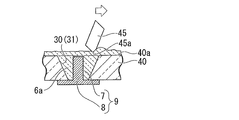
- a setting step (first scanning step) for filling the paste-like glass frit 6a into the through holes 30 and 31 is performed (S34A).
- a through hole 30 is obtained by scanning a resin squeegee along the surface 40a of the base substrate wafer 40 in a chamber (both not shown) of a vacuum screen printer maintained in a reduced-pressure atmosphere.
- 31 is filled with glass frit 6a.
- the vacuum screen printing machine of this embodiment includes a first squeegee 45 (see FIG. 14) and a second squeegee 46 (see FIG. 16) having the same shape, and scans in a direction in which they face each other by a moving mechanism (not shown). Held possible.
- the base substrate wafer 40 is transferred into the chamber, and the glass frit 6a is applied to the through holes 30 and 31. At this time, a large amount is applied so that the glass frit 6a is reliably filled in the through holes 30 and 31. Therefore, the glass frit 6 a is also applied to the surface 40 a of the base substrate wafer 40. Thereafter, the pressure in the chamber is reduced to about 1 torr, whereby the glass frit 6a is degassed, and bubbles contained in the glass frit 6a are removed.
- the glass frit 6a used in the present embodiment is a mixture of a glass material and a resin material such as ethyl cellulose for imparting thixotropy in an organic solvent such as butyl carbitol.
- the first squeegee 45 is scanned from one direction end to the other end side (see arrows in FIGS. 14 and 15).
- the surface direction of the base substrate wafer 40 and the scanning surface of the first squeegee 45 are set with the contact angle (attack angle) between the first squeegee 45 and the base substrate wafer 40 set to about 5 to 60 degrees.
- the first squeegee 45 is scanned so as to be parallel to each other.
- the scanning speed of the first squeegee 45 and the first are set so that the viscosity of the glass frit 6a is 10 Pa ⁇ s to 200 Pa ⁇ s. It is preferable to set a pressing force acting on the glass frit 6a from the tip 45a of the squeegee 45.
- the scanning speed of the first squeegee 45 is preferably set to 1 mm / sec or more and 10 mm / sec or less, and the glass frit from the tip 45a of the first squeegee 45 is set.
- the pressing force (linear pressure) acting on 6a is preferably set to 1 mg / mm or more and 1000 mg / mm. If the scanning speed of the first squeegee 45 is set to less than 1 mm / sec or the pressing force is set to less than 1 mg / mm, the above-mentioned desired viscosity cannot be obtained, and the glass frit 6a is smoothly placed in the through holes 30 and 31. Since there is a possibility that it may not enter, it is not preferable. On the other hand, if the scanning speed of the first squeegee 45 is faster than 10 mm / sec, it is difficult to push the glass frit 6a into the through holes 30 and 31, which is not preferable.
- the pressing force is set to be larger than 1000 mg / mm, it is not preferable because the base substrate wafer 40 is overloaded.
- the viscosity of the glass frit 6a is set to, for example, 60 Pa ⁇ s. Accordingly, the scanning speed of the first squeegee 45 is set to 10 mm / sec, and the pressing force is set to about 73 mg / mm. .
- the glass frit 6a flows so as to be pushed along the scanning direction of the first squeegee 45 (see the arrow in FIG. 14) by the tip 45a of the first squeegee 45. .
- the glass frit 6a is leveled along the base substrate wafer 40 as shown in FIG.
- the glass frit 6 a in the vicinity of the opening edge is pushed into the through holes 30 and 31 by the tip 45 a of the first squeegee 45. To flow.
- the glass frit 6a is filled in the through holes 30 and 31 without a gap.
- the base portion 8 since the base portion 8 is in contact with the front surface 40a of the base substrate wafer 40, the glass frit 6a does not overflow from the back surface side of the base substrate wafer 40, and the glass frit 6a is securely inserted into the through holes 30 and 31. Can be filled.
- the base portion 8 since the base portion 8 is formed in a flat plate shape, even if the base substrate wafer 40 is placed on a flat surface such as a desk between the setting step and the subsequent baking step, the base portion 8 is rattled. There is no etc. and it is stable. Also in this respect, workability can be improved.
- the glass frit 6a of the present embodiment is configured by mixing a glass material or a resin material in an organic solvent.
- an extremely reduced pressure atmosphere for example, less than 20 torr
- the organic solvent in the glass frit 6a may be evaporated and removed.
- the viscosity of the glass frit 6a remaining outside the through holes 30 and 31 increases, making it difficult to remove the glass frit 6a in the removal step.
- the pressure in the chamber is increased in the removal step (S34B) compared to the setting step (S34A).
- the pressure in the chamber at this time is preferably set to a pressure that does not evaporate the organic solvent of the glass frit 6a, and is preferably increased to about 30 torr, for example.
- the removal step (S34B) can be performed while preventing the glass frit 6a from evaporating.
- the second squeegee 46 is scanned along the surface 40a of the base substrate wafer 40 as shown in FIG. Specifically, with the tip 46a of the second squeegee 46 being in contact with the surface 40a of the base substrate wafer 40, the scanning direction of the first squeegee 45 is determined according to the same conditions as the scanning conditions of the first squeegee 45 described above. Scans in the opposite direction, that is, along the one end side from the other end side in the radial direction of the base substrate wafer 40 (see arrow in FIG. 16).
- the second squeegee 46 is scanned so that the glass frit 6 a existing on the surface 40 a of the base substrate wafer 40 existing outside the through holes 30 and 31 is scooped by the tip 46 a of the second squeegee 46.
- the excess glass frit 6a existing on the surface 40a of the base substrate wafer 40 can be removed with a simple operation.
- the second squeegee 46 since the length of the core portion 7 of the housing 9 is 0.02 mm shorter than the thickness of the base substrate wafer 40, the second squeegee 46 passes through the upper portions of the through holes 30 and 31.
- the tip 45a of the squeegee 45 and the tip of the core member 7 are not in contact with each other, and the core member 7 can be prevented from being inclined.
- a firing step of firing the embedded glass frit 6a at a predetermined temperature is performed (S35).
- the through holes 30 and 31, the glass frit 6a embedded in the through holes 30 and 31, and the housing 9 disposed in the glass frit 6a are fixed to each other.
- the base portion 8 is fired together, so that the axial direction of the core material portion 7 and the axial directions of the through holes 30 and 31 are substantially matched, and both are fixed integrally. Can do.
- the glass frit 6a is baked, it is solidified as the cylindrical body 6.
- a polishing step is performed to polish and remove the base portion 8 of the casing 9 after firing (S36).
- the base part 8 which played the role which positioned the cylinder 6 and the core material part 7 can be removed, and only the core material part 7 can be left inside the cylinder 6.
- the surface 40a of the base substrate wafer 40 is polished to become a flat surface. And it grind
- FIG. 19 it is possible to obtain a plurality of pairs of through electrodes 32 and 33 in which the cylindrical body 6 and the core member 7 are integrally fixed.
- the through electrode 32 is formed of the cylindrical body 6 made of a glass material and the conductive core material portion 7 without using a paste for the conductive portion. , 33 are formed. If a paste is used for the conductive part, the organic matter contained in the paste evaporates during firing, so the volume of the paste is significantly reduced compared to before firing. Therefore, if only the paste is embedded in the through holes 30 and 31, a large dent will be formed on the surface of the paste after firing. However, in this embodiment, since the metal core part 7 is used for the conductive part, the volume reduction of the conductive part can be eliminated.
- the surface of the base substrate wafer 40 and both ends of the cylindrical body 6 and the core member 7 are substantially flush with each other. That is, the surface of the base substrate wafer 40 and the surfaces of the through electrodes 32 and 33 can be substantially flush with each other.
- the polishing step (S36) is performed, the through electrode forming step (S30A) is completed.
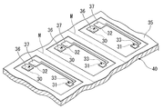
- FIG. 20 is a diagram showing a state in which the bonding film and the routing electrode are patterned on the upper surface of the base substrate wafer. Note that a broken line M in the figure indicates a contour line of the piezoelectric vibrator 1.
- a conductive material is patterned on the upper surface of the base substrate wafer 40, and as shown in FIG. 20, a bonding film forming step for forming the bonding film 35 is performed (S37), and each of the pair of through electrodes 32, A routing electrode forming step for forming a plurality of routing electrodes 36 and 37 that are electrically connected to 33 is performed (S38).
- the through electrodes 32 and 33 are substantially flush with the upper surface of the base substrate wafer 40 as described above.
- the routing electrodes 36 and 37 patterned on the upper surface of the base substrate wafer 40 are in close contact with the through electrodes 32 and 33 without generating a gap or the like therebetween. As a result, it is possible to ensure the electrical conductivity between the one routing electrode 36 and the one through electrode 32 and the electrical conductivity between the other routing electrode 37 and the other through electrode 33. At this point, the second wafer manufacturing process is completed.
- a mounting step (S40) is performed in which the piezoelectric vibrating reed 4 is bonded to the lead electrodes 36 and 37 of the base substrate wafer 40 via the bumps B. Thereafter, the lid substrate wafer is applied to the base substrate wafer 40.
- S50 superposition step. After the superposition process, the two superposed wafers 40 are put into an anodic bonding apparatus (not shown), and a predetermined voltage is applied in a predetermined temperature atmosphere to perform anodic bonding to form a wafer bonded body (S60: bonding process). .
- the through holes 30 and 31 formed in the base substrate wafer 40 are completely closed by the through electrodes 32 and 33, so that the airtightness in the cavity C is reduced. Will not be damaged through.
- the cylindrical body 6 and the core member 7 are fixedly fixed by firing, and these are firmly fixed to the through holes 30 and 31, so that the airtightness in the cavity C is reliably maintained. can do.
- a conductive material is patterned on the lower surface of the base substrate wafer 40 to form a pair of external electrodes 38 and 39 electrically connected to the pair of through electrodes 32 and 33, respectively.
- a plurality of external electrode forming steps are formed (S70).
- the through electrodes 32 and 33 are substantially flush with the lower surface of the base substrate wafer 40 as in the formation of the lead-out electrodes 36 and 37.
- the external electrodes 38 and 39 are in close contact with the through electrodes 32 and 33 without generating a gap or the like therebetween. Thereby, the continuity between the external electrodes 38 and 39 and the through electrodes 32 and 33 can be ensured.
- the pasty glass frit 6a is filled into the through holes 30 and 31 in a reduced pressure atmosphere.
- the glass frit 6a is degassed, and bubbles contained in the glass frit 6a can be removed. As a result, no bubbles are present in the glass frit 6a, and no air is present in the through holes 30 and 31.
- the glass frit 6a is pushed away by the first squeegee 45, so that the glass frit in the through holes 30 and 31 is filled in the through holes 30 and 31 as compared with the conventional case where the glass frit 6a is filled in the atmosphere. 6a can be filled smoothly. As a result, the glass frit 6a can be filled in the through holes 30 and 31 without a gap. By firing the glass frit 6a in this state, the through holes 30 and 31 can be sealed without gaps by the cylindrical body 6 formed after firing, so that the airtightness in the cavity C is maintained in a good state. can do.
- the core member 7 can be firmly fixed at a predetermined position, so that the through electrodes 32 and 33 having desired dimensions can be formed. Accordingly, the external electrodes 38 and 39 and the through electrodes 32 and 33 are in close contact with each other without generating a gap. As a result, disconnection of the external electrodes 38 and 39 formed so as to cover the through electrodes 32 and 33 can be prevented, and the piezoelectric vibrating reed 4 and the external electrodes 38 and 39 can be prevented from passing through the through electrodes 32 and 33. Conductivity can be ensured.
- the vibration characteristics of the piezoelectric vibrator 1 are not deteriorated. Therefore, it is possible to collectively manufacture the piezoelectric vibrators 1 that are small in size and excellent in vibration characteristics and highly reliable on the wafer while improving the yield.
- the viscosity of the glass frit 6a is reduced by performing the setting step (S34A) in the chamber under the above-described conditions.
- the fluidity can be improved. Accordingly, the glass frit 6 a can be pushed more smoothly into the through holes 30 and 31.
- the oscillator 100 is configured such that the piezoelectric vibrator 1 is an oscillator electrically connected to the integrated circuit 101.
- the oscillator 100 includes a substrate 103 on which an electronic component 102 such as a capacitor is mounted. On the substrate 103, the above-described integrated circuit 101 for the oscillator is mounted, and the piezoelectric vibrator 1 is mounted in the vicinity of the integrated circuit 101.
- the electronic component 102, the integrated circuit 101, and the piezoelectric vibrator 1 are electrically connected by a wiring pattern (not shown). Each component is molded with a resin (not shown).
- the piezoelectric vibrating reed 4 in the piezoelectric vibrator 1 vibrates. This vibration is converted into an electric signal by the piezoelectric characteristics of the piezoelectric vibrating piece 4 and input to the integrated circuit 101 as an electric signal.
- the input electrical signal is subjected to various processes by the integrated circuit 101 and is output as a frequency signal.
- the piezoelectric vibrator 1 functions as an oscillator.
- an RTC real-time clock
- a function for controlling the time, providing a time, a calendar, and the like can be added.
- the quality of the oscillator 100 itself can be improved in the same manner. In addition to this, it is possible to obtain a highly accurate frequency signal that is stable over a long period of time.
- the portable information device 110 having the above-described piezoelectric vibrator 1 will be described as an example of the electronic device.
- the portable information device 110 according to the present embodiment is represented by, for example, a mobile phone, and is a development and improvement of a wrist watch in the related art. The appearance is similar to that of a wristwatch, and a liquid crystal display is arranged in a portion corresponding to a dial so that the current time and the like can be displayed on this screen.
- the portable information device 110 includes the piezoelectric vibrator 1 and a power supply unit 111 for supplying power.
- the power supply unit 111 is made of, for example, a lithium secondary battery.
- the power supply unit 111 includes a control unit 112 that performs various controls, a clock unit 113 that counts time, a communication unit 114 that communicates with the outside, a display unit 115 that displays various types of information, A voltage detection unit 116 that detects the voltage of the functional unit is connected in parallel.
- the power unit 111 supplies power to each functional unit.
- the control unit 112 controls each function unit to control operation of the entire system such as transmission and reception of voice data, measurement and display of the current time, and the like.
- the control unit 112 includes a ROM in which a program is written in advance, a CPU that reads and executes the program written in the ROM, and a RAM that is used as a work area of the CPU.
- the clock unit 113 includes an integrated circuit including an oscillation circuit, a register circuit, a counter circuit, an interface circuit, and the like, and the piezoelectric vibrator 1.
- the piezoelectric vibrating piece 4 vibrates, and this vibration is converted into an electric signal by the piezoelectric characteristics of the crystal and is input to the oscillation circuit as an electric signal.
- the output of the oscillation circuit is binarized and counted by a register circuit and a counter circuit. Then, signals are transmitted to and received from the control unit 112 via the interface circuit, and the current time, current date, calendar information, or the like is displayed on the display unit 115.
- the communication unit 114 has functions similar to those of a conventional mobile phone, and includes a radio unit 117, a voice processing unit 118, a switching unit 119, an amplification unit 120, a voice input / output unit 121, a telephone number input unit 122, and a ring tone generation unit. 123 and a call control memory unit 124.
- the wireless unit 117 exchanges various data such as audio data with the base station via the antenna 125.
- the audio processing unit 118 encodes and decodes the audio signal input from the radio unit 117 or the amplification unit 120.
- the amplifying unit 120 amplifies the signal input from the audio processing unit 118 or the audio input / output unit 121 to a predetermined level.
- the voice input / output unit 121 includes a speaker, a microphone, and the like, and amplifies a ringtone and a received voice or collects a voice.
- the ring tone generator 123 generates a ring tone in response to a call from the base station.
- the switching unit 119 switches the amplifying unit 120 connected to the voice processing unit 118 to the ringing tone generating unit 123 only when an incoming call is received, so that the ringing tone generated in the ringing tone generating unit 123 is transmitted via the amplifying unit 120.
- the call control memory unit 124 stores a program related to incoming / outgoing call control of communication.
- the telephone number input unit 122 includes, for example, a number key from 0 to 9 and other keys. By pressing these number keys and the like, a telephone number of a call destination is input.
- the voltage detection unit 116 detects the voltage drop and notifies the control unit 112 of the voltage drop.
- the predetermined voltage value at this time is a value set in advance as a minimum voltage necessary for stably operating the communication unit 114, and is, for example, about 3V.
- the control unit 112 prohibits the operations of the radio unit 117, the voice processing unit 118, the switching unit 119, and the ring tone generation unit 123. In particular, it is essential to stop the operation of the wireless unit 117 with high power consumption. Further, the display unit 115 displays that the communication unit 114 has become unusable due to insufficient battery power.
- the operation of the communication unit 114 can be prohibited by the voltage detection unit 116 and the control unit 112, and that effect can be displayed on the display unit 115.
- This display may be a text message, but as a more intuitive display, a x (X) mark may be attached to the telephone icon displayed at the top of the display surface of the display unit 115.
- the function of the communication part 114 can be stopped more reliably by providing the power supply cutoff part 126 that can selectively cut off the power of the part related to the function of the communication part 114.
- the portable information device 110 of the present embodiment since the high-quality piezoelectric vibrator 1 is provided, the quality of the portable information device itself can be improved as well. In addition to this, it is possible to display highly accurate clock information that is stable over a long period of time.
- the radio timepiece 130 of this embodiment includes the piezoelectric vibrator 1 that is electrically connected to the filter unit 131.
- the radio timepiece 130 receives a standard radio wave including timepiece information and is accurate. It is a clock with a function of automatically correcting and displaying the correct time.
- transmitting stations transmitting stations that transmit standard radio waves in Fukushima Prefecture (40 kHz) and Saga Prefecture (60 kHz), each transmitting standard radio waves.
- Long waves such as 40 kHz or 60 kHz have the property of propagating the surface of the earth and the property of propagating while reflecting the ionosphere and the surface of the earth, so the propagation range is wide, and the above two transmitting stations cover all of Japan. is doing.
- the antenna 132 receives a long standard wave of 40 kHz or 60 kHz.
- the long-wave standard radio wave is obtained by subjecting time information called a time code to AM modulation on a 40 kHz or 60 kHz carrier wave.
- the received long standard wave is amplified by the amplifier 133 and filtered and tuned by the filter unit 131 having the plurality of piezoelectric vibrators 1.
- the piezoelectric vibrator 1 in this embodiment includes crystal vibrator portions 138 and 139 having resonance frequencies of 40 kHz and 60 kHz that are the same as the carrier frequency described above.
- the filtered signal having a predetermined frequency is detected and demodulated by the detection and rectification circuit 134. Subsequently, the time code is taken out via the waveform shaping circuit 135 and counted by the CPU 136.
- the CPU 136 reads information such as the current year, accumulated date, day of the week, and time. The read information is reflected in the RTC 137, and accurate time information is displayed. Since the carrier wave is 40 kHz or 60 kHz, the crystal vibrator units 138 and 139 are preferably vibrators having the tuning fork type structure described above.
- the frequency of the long standard radio wave is different overseas.
- a standard radio wave of 77.5 KHz is used. Accordingly, when the radio timepiece 130 that can be used overseas is incorporated in a portable device, the piezoelectric vibrator 1 having a frequency different from that in Japan is required.
- the radio-controlled timepiece 130 of the present embodiment since the high-quality piezoelectric vibrator 1 is provided, the quality of the radio-controlled timepiece itself can be improved in the same manner. In addition to this, it is possible to count time stably and with high accuracy over a long period of time.
- the tuning fork type piezoelectric vibrating piece 4 has been described as an example, but is not limited to the tuning fork type.
- a through-electrode may be formed by the above-described method when a thickness-shear vibration piece or an AT vibration piece is mounted in a cavity and these vibration pieces and an external electrode are electrically connected.
- the two-layer structure type in which the piezoelectric vibrating reed 4 is housed in the cavity C formed between the base substrate 2 and the lid substrate 3 has been described. It is also possible to adopt a three-layer structure type in which the piezoelectric substrate on which the resonator element 4 is formed is joined between the base substrate 2 and the lid substrate 3 so as to be sandwiched from above and below. Further, in the above-described embodiment, the case where the glass frit 6a serving as the filler is filled between the core portion 7 and the through holes 30 and 31 has been described. However, the present invention is not limited thereto, and a conductive filler is used. The through holes 30 and 31 may be filled and the structure itself may be a through electrode. As such a filler, one containing metal fine particles and a plurality of glass beads or the above-described conductive paste can be used.
- the grooved piezoelectric vibrating piece 4 in which the groove portions 18 are formed on both surfaces of the vibrating arm portions 10 and 11 has been described as an example, but the groove portion 18 is not provided.
- a type of piezoelectric vibrating piece may be used.
- the groove portion 18 is formed so that the electric field efficiency between the pair of excitation electrodes 15 can be increased when a predetermined voltage is applied to the pair of excitation electrodes 15, vibration loss is further suppressed and vibration characteristics are reduced. Can be further improved. That is, the CI value (Crystal Impedance) can be further lowered, and the piezoelectric vibrating piece 4 can be further improved in performance.
- the piezoelectric vibrating reed 4 is bump-bonded, but is not limited to bump bonding.
- the piezoelectric vibrating reed 4 may be joined with a conductive adhesive.
- the piezoelectric vibrating reed 4 can be lifted from the upper surface of the base substrate 2, and the minimum vibration gap necessary for vibration can be secured naturally. Therefore, it is preferable to perform bump bonding.
Landscapes
- Physics & Mathematics (AREA)
- Acoustics & Sound (AREA)
- Chemical & Material Sciences (AREA)
- Crystallography & Structural Chemistry (AREA)
- Piezo-Electric Or Mechanical Vibrators, Or Delay Or Filter Circuits (AREA)
- Oscillators With Electromechanical Resonators (AREA)
Abstract
Description
このような2層構造タイプの圧電振動子の一つとして、ベース基板を貫通するように形成された導電部材を利用して、圧電振動片とベース基板に形成された外部電極とを導通させた圧電振動子が知られている(例えば、特許文献1および特許文献2参照)。
ベース基板201およびリッド基板202は、例えばセラミックやガラスなどからなる絶縁基板である。両基板201、202のうちベース基板201には、基板201を貫通するスルーホール204が形成されている。そして、このスルーホール204内には、スルーホール204を塞ぐように導電部材205が埋め込まれている。この導電部材205は、ベース基板201の下面に形成された外部電極206に電気的に接続されているとともに、キャビティC内にマウントされている圧電振動片203に電気的に接続されている。
しかしながら、導電ペーストの充填後に焼成を行うと、導電ペーストに含まれる有機物が蒸発により消失してしまう。その結果、焼成後の導電ペーストの体積が焼成前に比べて減少するため、導電ペーストにより形成された導電部材205の表面に凹みが発生してしまったり、ひどい場合には貫通孔が中心に開いてしまったりする虞がある。
すなわち、スルーホール204にピンを配置した状態で、スキージを用いて充填材を充填しようとすると、充填材とともに大気中の空気がスルーホール204内に押し込まれ、スルーホール204が充填材によって閉塞される。そのため、スルーホール204内の空気が抜け切らず、充填材がスルーホール204内に十分に充填されないという問題がある。
また、充填材中に存在する気泡がスルーホール204内に入り込み、これによっても充填材が十分に充填されないという問題がある。また、その後焼成によって気泡が蒸発することで、焼成後の体積が焼成前に比べて大幅に減少してしまう。これにより、上述したように焼成された充填材の表面に凹みが発生してしまったりする虞がある。
また、充填材の焼成後に、スルーホール204内に残存する空気がキャビティC中に漏出すると、圧電振動子200の振動特性が低下するという問題がある。
本発明に係るパッケージの製造方法は、互いに接合された複数の基板との間に形成されたキャビティ内に、電子部品を封入可能なパッケージの製造方法であって、前記複数の基板のうち、第1基板を厚さ方向に貫通し、前記キャビティの内側と前記パッケージの外側とを導通する貫通電極を形成する貫通電極形成工程を有し、前記貫通電極形成工程は、前記第1基板に前記貫通電極を配するための貫通孔を形成する貫通孔形成工程と、減圧雰囲気下において、前記貫通孔内に充填材を充填する充填工程とを有することを特徴としている。
また、充填材の焼成後に貫通孔内に残存する空気がキャビティ内に漏出することもないので、パッケージの特性が低下することもない。
したがって、歩留まりを向上させた上で、小型で信頼性の高いパッケージを製造することができる。
ところで、極度の減圧雰囲気下に長時間充填材を曝しておくと、充填材に含まれる成分(例えば、有機溶剤)が蒸発して除去される虞がある。その結果、貫通孔の外側に残存する充填材の粘度が上昇して、第2走査工程において充填材を除去し難くなる。
これに対して、本発明の構成によれば、第2走査工程では第1走査工程に比べて、チャンバー内を昇圧することで、充填材に含まれる成分の蒸発を防ぐことができるので、充填材の粘度の上昇を防ぎ、第2走査工程をスムーズに行うことができる。
この構成によれば、貫通孔内に導電性の芯材部を配置することで、焼成後の体積減少が芯材部と貫通孔との間に充填された充填材の部分のみになるため、芯材部は第1基板の表面に対して面一な状態となる。これにより、芯材部に接続される外部電極との間に隙間を生じさせることがなく、貫通電極と外部電極との導通を確保することができる。
また、土台部上に芯材部が形成された鋲体を利用するため、土台部を第1基板に接触させるまで押し込むだけの簡単な作業で、芯材部の軸方向と貫通孔の軸方向とを略一致させることができる。したがって、鋲体セット工程時における作業性を向上することができる。さらに、後に行う焼成工程までの間に、第1基板を机上等の平面上に載置したとしても、がたつき等がなく、安定する。この点においても、作業性の向上を図ることができる。
特に、本発明の構成によれば、貫通孔内にガラスフリットを隙間なく充填することができるため、その後にガラスフリットを焼成することによって、貫通孔を隙間なく封止することができる。その結果、キャビティ内の気密を良好な状態に維持することができる。また、焼成後の体積減少や変形も生じにくいので、芯材部を所定位置に強固に固着することができる。その結果、高品質な貫通電極を形成することができ、電子部品と外部電極との導通性を確保することができる。
この構成によれば、ガラスフリットの粘度を、10Pa・s以上200Pa・s以下に設定することで、ガラスフリットの流動性を向上させ、充填工程において充填材をスムーズに貫通孔内に充填することができる。
スキージの走査速度を1mm/sec未満に設定すると、上述した所望の粘度を得ることができず、貫通孔内にガラスフリットがスムーズに入り込んでいかない虞があるため好ましくない。
一方、スキージの走査速度を10mm/secより早くすると、貫通孔内にガラスフリットが入り難くなるため好ましくない。
これに対して、スキージの走査速度を、1mm/sec以上50mm/sec以下に設定することで、ガラスフリットを上述した所望の粘度に設定することができるので、ガラスフリットの流動性を向上させ、第1走査工程において充填材をスムーズに貫通孔内に充填することができる。
この構成によれば、スキージからガラスフリットに作用する線圧力を1mm/sec未満に設定すると、上述した所望の粘度を得ることができず、貫通孔内にガラスフリットがスムーズに入り込んでいかない虞があるため好ましくない。
一方、押圧力を1000mg/mmより大きく設定すると、第1基板に過負荷がかかるため好ましくない。
これに対して、スキージからガラスフリットに作用する線圧力を、1mg/mm以上1000mg/mm以下に設定することで、ガラスフリットを上述した所望の粘度に設定することができるので、ガラスフリットの流動性を向上させ、第1走査工程において充填材をスムーズに貫通孔内に充填することができる。
この構成によれば、上記本発明のパッケージの製造方法によって製造された圧電振動子であるため、小型で信頼性の高い圧電振動子を提供することができる。
また、充填材の焼成後に貫通孔内に残存する空気がキャビティ内に漏出することもないので、パッケージの特性が低下することもない。
したがって、歩留まりを向上させた上で、小型で信頼性の高いパッケージを製造することができる。
また、本発明に係る圧電振動子によれば、上記本発明のパッケージの製造方法によって製造された圧電振動子であるため、小型で信頼性の高い圧電振動子を提供することができる。
本発明に係る発振器、電子機器及び電波時計においては、上述した圧電振動子を備えているので、小型で信頼性の高い製品を提供することができる。
(圧電振動子)
図1は本発明に係る圧電振動子の外観斜視図であり、図2は圧電振動子の内部構成図であって、リッド基板を取り外した状態で圧電振動片を上方から見た図ある。また、図3は図2に示すA-A線に沿った圧電振動子の断面図であり、図4は圧電振動子の分解斜視図である。
図1~4に示すように、本実施形態の圧電振動子1は、ベース基板(第1基板)2とリッド基板(第2基板)3とで2層に積層された箱状に形成されており、内部のキャビティC(図4参照)内に圧電振動片4が収納された表面実装型の圧電振動子である。なお、図4においては、図面を見易くするために後述する励振電極15、引き出し電極19,20、マウント電極16,17及び重り金属膜21の図示を省略している。
図5~7に示すように、圧電振動片4は、水晶、タンタル酸リチウムやニオブ酸リチウム等の圧電材料から形成された音叉型の振動片であり、所定の電圧が印加されたときに振動するものである。
この圧電振動片4は、平行に配置された一対の振動腕部10,11と、一対の振動腕部10,11の基端側を一体的に固定する基部12と、一対の振動腕部10,11の外表面上に形成されて一対の振動腕部10,11を振動させる第1の励振電極13と第2の励振電極14とからなる励振電極15と、第1の励振電極13及び第2の励振電極14に電気的に接続されたマウント電極16,17とを有している。
また、本実施形態の圧電振動片4は、一対の振動腕部10,11の両主面上に、振動腕部10,11の長手方向に沿ってそれぞれ形成された溝部18を備えている。この溝部18は、振動腕部10,11の基端側から略中間付近まで形成されている。
また、第1の励振電極13及び第2の励振電極14は、基部12の両主面上において、それぞれ引き出し電極19,20を介してマウント電極16,17に電気的に接続されている。
このベース基板2には、ベース基板2を厚さ方向に貫通する一対のスルーホール(貫通孔)30,31が形成されている。この際、一対のスルーホール30,31は、キャビティC内に収まるように形成されている。より詳しく説明すると、本実施形態のスルーホール30,31は、マウントされた圧電振動片4の基部12側に対応した位置に一方のスルーホール30が形成され、振動腕部10,11の先端側に対応した位置に他方のスルーホール31が形成されている。また、本実施形態では、ベース基板2の下面から上面に向かって漸次径が縮径した断面テーパ状のスルーホールを例に挙げて説明するが、この場合に限られず、ベース基板2を真っ直ぐに貫通するスルーホールでも構わない。いずれにしても、ベース基板2を貫通していれば良い。
図8に示すように、筒体6は、ペースト状のガラスフリット6a(図14参照)が焼成されたものである。筒体6は、両端が平坦で且つベース基板2と略同じ厚みの円筒状に形成されている。そして、筒体6の中心には、芯材部7が筒体6を貫通するように配されている。また、本実施形態ではスルーホール30,31の形状に合わせて、筒体6の外形が円錐状(断面テーパ状)となるように形成されている。そして、この筒体6は、図4に示すように、スルーホール30,31内に埋め込まれた状態で焼成されており、スルーホール30,31に対して強固に固着されている。
なお、貫通電極32,33は、導電性の芯材部7を通して電気導通性が確保されている。
そして、これら一対の引き回し電極36,37上にそれぞれバンプBが形成されており、バンプBを利用して圧電振動片4がマウントされている。これにより、圧電振動片4の一方のマウント電極16が、一方の引き回し電極36を介して一方の貫通電極32に導通し、他方のマウント電極17が、他方の引き回し電極37を介して他方の貫通電極33に導通するようになっている。
次に、図9に示すフローチャートを参照しながら、ベース基板2となるベース基板用ウエハ40と、リッド基板3となるリッド基板用ウエハとを利用して一度に複数の圧電振動子1を製造する製造方法について以下に説明する。
ここで、貫通電極形成工程(S30A)について、詳細に説明する。
まず、図10,11に示すように、ベース基板用ウエハ40を貫通する一対のスルーホール30,31を複数形成する貫通孔形成工程(S32)を行う。なお、図10に示す破線Mは、後に行う切断工程で切断する切断線を図示している。この工程を行う際、ベース基板用ウエハ40の下面側から、例えばサンドブラスト法やプレス加工等で行う。これにより、図11に示すように、ベース基板用ウエハ40の下面から上面に向かって漸次径が縮径する断面テーパ状のスルーホール30,31を形成することができる。また、後に両ウエハ40を重ね合わせたときに、リッド基板用ウエハに形成された凹部3a内に収まるように一対のスルーホール30,31を複数形成する。しかも、一方のスルーホール30が圧電振動片4の基部12側に位置し、他方のスルーホール31が振動腕部10,11の先端側に位置するように形成する。
続いて、これら複数のスルーホール30,31内に、鋲体9の芯材部7を配置する鋲体セット工程を行う(S33)。この際、鋲体9として、図12に示すように、平板状の土台部8と、土台部8上から土台部8の表面に略直交する方向に沿ってベース基板用ウエハ40の厚さよりも0.02mmだけ短い長さで形成されるとともに、先端が平坦に形成された芯材部7と、を有する導電性の鋲体9を用いる。さらに、図13に示すように、この鋲体9の土台部8の表面がベース基板用ウエハ40に接触するまで、芯材部7を挿入する。ここで、芯材部7の軸方向とスルーホール30,31の軸方向とを略一致するように鋲体9を配置する必要がある。しかしながら、土台部8上に芯材部7が形成された鋲体9を利用するため、土台部8をベース基板用ウエハ40に接触させるまで押し込むだけの簡単な作業で、芯材部7の軸方向とスルーホール30,31の軸方向とを略一致させることができる。したがって、鋲体セット工程時における作業性を向上することができる。
充填工程(S34)において、まず、ペースト状のガラスフリット6aをスルーホール30,31内に充填するセット工程(第1走査工程)を行う(S34A)。このセット工程では、減圧雰囲気下に維持された真空スクリーン印刷機のチャンバー(ともに不図示)内において、ベース基板用ウエハ40の表面40aに沿って樹脂製のスキージを走査することにより、スルーホール30,31内にガラスフリット6aを充填する。なお、本実施形態の真空スクリーン印刷機は、同一形状からなる第1スキージ45(図14参照)及び第2スキージ46(図16参照)を備え、図示しない移動機構により互いが対向する方向に走査可能に保持されている。
なお、本実施形態では、ガラスフリット6aの粘度が例えば60Pa・sに設定されており、これに伴い第1スキージ45の走査速度を10mm/sec、押圧力を73mg/mm程度に設定している。
さらに、土台部8は、平板状に形成されているため、セット工程後、後に行う焼成工程までの間に、ベース基板用ウエハ40を机上等の平面上に載置したとしても、がたつき等がなく、安定する。この点においても、作業性の向上を図ることができる。
セット工程(S34A)を行った状態でガラスフリット6aを焼成すると、後の研磨工程に要する時間が多くなるため、焼成前に余分なガラスフリット6aを除去する除去工程(S34B:第2走査工程)を行う。
ところで、上述したように本実施形態のガラスフリット6aは、ガラス材料や樹脂材料が有機溶剤に混入されて構成されている。この場合、極度の減圧雰囲気下(例えば、20torr未満)に長時間ガラスフリット6aを曝しておくと、ガラスフリット6aの有機溶剤が蒸発して除去される虞がある。その結果、スルーホール30,31の外側に残存するガラスフリット6aの粘度が上昇して、除去工程においてガラスフリット6aを除去し難くなる。
このようにすることで、図17に示すように、簡易な作業でベース基板用ウエハ40の表面40aに存在する余分なガラスフリット6aを除去することができる。そして、本実施形態では鋲体9の芯材部7の長さをベース基板用ウエハ40の厚さよりも0.02mm短くしたため、第2スキージ46がスルーホール30,31の上部を通過する際に、スキージ45の先端45aと芯材部7の先端とが接触することがなくなり、芯材部7が傾いてしまうことを抑制することができる。
また、同時にベース基板用ウエハ40の表面40aを研磨して平坦面になるようにする。そして、芯材部7の先端が露出するまで研磨する。その結果、図19に示すように、筒体6と芯材部7とが一体的に固定された一対の貫通電極32,33を複数得ることができる。
次に、ベース基板用ウエハ40の上面に導電性材料をパターニングして、図20に示すように、接合膜35を形成する接合膜形成工程を行う(S37)とともに、各一対の貫通電極32,33にそれぞれ電気的に接続された引き回し電極36,37を複数形成する引き回し電極形成工程を行う(S38)。
特に、貫通電極32,33は、上述したようにベース基板用ウエハ40の上面に対して略面一な状態となっている。そのため、ベース基板用ウエハ40の上面にパターニングされた引き回し電極36,37は、間に隙間等を発生させることなく貫通電極32,33に対して密着した状態で接する。これにより、一方の引き回し電極36と一方の貫通電極32との導通性、並びに、他方の引き回し電極37と他方の貫通電極33との導通性を確実なものにすることができる。この時点で第2のウエハ作製工程が終了する。
重ね合わせ工程後、重ね合わせた2枚のウエハ40を図示しない陽極接合装置に入れ、所定の温度雰囲気で所定の電圧を印加して陽極接合し、ウエハ接合体を形成する(S60:接合工程)。ところで、陽極接合を行う際、ベース基板用ウエハ40に形成されたスルーホール30,31は、貫通電極32,33によって完全に塞がれているため、キャビティC内の気密がスルーホール30,31を通じて損なわれることがない。しかも、焼成によって筒体6と芯材部7とが一定的に固定されているとともに、これらがスルーホール30,31に対して強固に固着されているため、キャビティC内の気密を確実に維持することができる。
特に、この工程を行う場合も引き回し電極36,37の形成時と同様に、ベース基板用ウエハ40の下面に対して貫通電極32,33が略面一な状態となっているため、パターニングされた外部電極38,39は、間に隙間等を発生させることなく貫通電極32,33に対して密着した状態で接する。これにより、外部電極38,39と貫通電極32,33との導通性を確実なものにすることができる。
周波数の微調が終了後、接合されたウエハ体を切断線Mに沿って切断して小片化する切断工程を行う(S90)。
その後、内部の電気特性検査(S100)を行うことで、圧電振動子1の製造が終了する。
この構成によれば、充填工程(S34)を減圧雰囲気下で行うことで、ガラスフリット6aが脱気され、ガラスフリット6a中に含まれる気泡を除去することができる。これにより、ガラスフリット6a内には気泡が存在しておらず、またスルーホール30,31内にも空気は存在しないことになる。そのため、セット工程(S34A)において、第1スキージ45によってガラスフリット6aを押し流すことで、従来のように大気中にてガラスフリット6aを充填する場合に比べて、スルーホール30,31内にガラスフリット6aをスムーズに充填することができる。その結果、スルーホール30,31内にガラスフリット6aを隙間なく充填することができる。
そして、この状態でガラスフリット6aを焼成することで、焼成後に形成された筒体6によってスルーホール30,31を隙間なく封止することができるので、キャビティC内の気密を良好な状態に維持することができる。また、焼成後の体積減少や変形も生じにくいので、芯材部7を所定位置に強固に固着することができるので、所望の寸法を有する貫通電極32,33を形成することができる。よって、外部電極38,39と貫通電極32,33との間に隙間を発生させることなく、両者は密着した状態で接する。その結果、貫通電極32,33を覆うように形成された外部電極38,39の段切れを防止することができ、貫通電極32,33を介して圧電振動片4と外部電極38,39との導通性を確保することができる。
また、ガラスフリット6aの焼成後に、スルーホール30,31内に残存する空気がキャビティC内に漏出することもないので、圧電振動子1の振動特性が低下することもない。
よって、歩留まりを向上させた上で、小型で振動特性に優れた信頼性の高い圧電振動子1をウエハ上で一括して製造することができる。
次に、本発明に係る発振器の一実施形態について、図15を参照しながら説明する。
本実施形態の発振器100は、図15に示すように、圧電振動子1を、集積回路101に電気的に接続された発振子として構成したものである。この発振器100は、コンデンサ等の電子部品102が実装された基板103を備えている。基板103には、発振器用の上述した集積回路101が実装されており、この集積回路101の近傍に、圧電振動子1が実装されている。これら電子部品102、集積回路101及び圧電振動子1は、図示しない配線パターンによってそれぞれ電気的に接続されている。なお、各構成部品は、図示しない樹脂によりモールドされている。
また、集積回路101の構成を、例えば、RTC(リアルタイムクロック)モジュール等を要求に応じて選択的に設定することで、時計用単機能発振器等の他、当該機器や外部機器の動作日や時刻を制御したり、時刻やカレンダー等を提供したりする機能を付加することができる。
次に、本発明に係る電子機器の一実施形態について、図16を参照して説明する。なお電子機器として、上述した圧電振動子1を有する携帯情報機器110を例にして説明する。始めに本実施形態の携帯情報機器110は、例えば、携帯電話に代表されるものであり、従来技術における腕時計を発展、改良したものである。外観は腕時計に類似し、文字盤に相当する部分に液晶ディスプレイを配し、この画面上に現在の時刻等を表示させることができるものである。また、通信機として利用する場合には、手首から外し、バンドの内側部分に内蔵されたスピーカ及びマイクロフォンによって、従来技術の携帯電話と同様の通信を行うことが可能である。しかしながら、従来の携帯電話と比較して、格段に小型化及び軽量化されている。
無線部117は、音声データ等の各種データを、アンテナ125を介して基地局と送受信のやりとりを行う。音声処理部118は、無線部117又は増幅部120から入力された音声信号を符号化及び複号化する。増幅部120は、音声処理部118又は音声入出力部121から入力された信号を、所定のレベルまで増幅する。音声入出力部121は、スピーカやマイクロフォン等からなり、着信音や受話音声を拡声したり、音声を集音したりする。
なお、呼制御メモリ部124は、通信の発着呼制御に係るプログラムを格納する。また、電話番号入力部122は、例えば、0から9の番号キー及びその他のキーを備えており、これら番号キー等を押下することにより、通話先の電話番号等が入力される。
なお、通信部114の機能に係る部分の電源を、選択的に遮断することができる電源遮断部126を備えることで、通信部114の機能をより確実に停止することができる。
本実施形態の電波時計130は、図17に示すように、フィルタ部131に電気的に接続された圧電振動子1を備えたものであり、時計情報を含む標準の電波を受信して、正確な時刻に自動修正して表示する機能を備えた時計である。
日本国内には、福島県(40kHz)と佐賀県(60kHz)とに、標準の電波を送信する送信所(送信局)があり、それぞれ標準電波を送信している。40kHz若しくは60kHzのような長波は、地表を伝播する性質と、電離層と地表とを反射しながら伝播する性質とを併せもつため、伝播範囲が広く、上述した2つの送信所で日本国内を全て網羅している。
以下、電波時計130の機能的構成について詳細に説明する。
アンテナ132は、40kHz若しくは60kHzの長波の標準電波を受信する。長波の標準電波は、タイムコードと呼ばれる時刻情報を、40kHz若しくは60kHzの搬送波にAM変調をかけたものである。受信された長波の標準電波は、アンプ133によって増幅され、複数の圧電振動子1を有するフィルタ部131によって濾波、同調される。
本実施形態における圧電振動子1は、上述した搬送周波数と同一の40kHz及び60kHzの共振周波数を有する水晶振動子部138、139をそれぞれ備えている。
続いて、波形整形回路135を介してタイムコードが取り出され、CPU136でカウントされる。CPU136では、現在の年、積算日、曜日、時刻等の情報を読み取る。読み取られた情報は、RTC137に反映され、正確な時刻情報が表示される。
搬送波は、40kHz若しくは60kHzであるから、水晶振動子部138、139は、上述した音叉型の構造を持つ振動子が好適である。
例えば、上述した実施形態では、音叉型の圧電振動片4を例に挙げて説明したが、音叉型に限られるものではない。例えば、厚み滑り振動片やAT振動片をキャビティ内にマウントし、これらの振動片と外部電極とを電気的に接続する際に、上述した方法により貫通電極を形成しても構わない。
また、上述した実施形態では、ベース基板2とリッド基板3との間に形成されたキャビティC内に圧電振動片4を収納した2層構造タイプのものについて説明したが、これに限らず、圧電振動片4が形成された圧電基板をベース基板2とリッド基板3とで上下から挟み込むように接合した3層構造タイプを採用することも可能である。
さらに、上述した実施形態では、芯材部7とスルーホール30,31との間に充填材となるガラスフリット6aを充填する場合について説明したが、これに限らず、導電性を有する充填材をスルーホール30,31に充填し、それ自体を貫通電極とする構成にしてもよい。このような充填材としては、金属微粒子および複数のガラスビーズを含んだものや、上述した導電ペーストを用いることが可能である。
また、上記実施形態では、圧電振動片4をバンプ接合したが、バンプ接合に限定されるものではない。例えば、導電性接着剤により圧電振動片4を接合しても構わない。ただし、バンプ接合することで、圧電振動片4をベース基板2の上面から浮かすことができ、振動に必要な最低限の振動ギャップを自然と確保することができる。よって、バンプ接合することが好ましい。
Claims (10)
- 互いに接合された複数の基板との間に形成されたキャビティ内に、電子部品を封入可能なパッケージの製造方法であって、
前記複数の基板のうち、第1基板を厚さ方向に貫通し、前記キャビティの内側と前記パッケージの外側とを導通する貫通電極を形成する貫通電極形成工程を有し、
前記貫通電極形成工程は、
前記第1基板に前記貫通電極を配するための貫通孔を形成する貫通孔形成工程と、
減圧雰囲気下において、前記貫通孔内に充填材を充填する充填工程とを有することを特徴とするパッケージの製造方法。 - 請求項1記載のパッケージの製造方法であって、
前記充填工程は、前記第1基板の表面に沿って前記第1基板の一端側から他端側へ第1スキージを走査して、前記充填材を前記貫通孔内に充填する第1走査工程と、
前記第1基板の表面に沿って前記第1基板の前記他端側から前記一端側へ第2スキージを走査させ、前記貫通孔の外部に存在する前記充填材を除去する第2走査工程とを有し、
前記第2走査工程における雰囲気圧力を、前記第1走査工程よりも高圧に設定することを特徴とするパッケージの製造方法。 - 請求項1または請求項2記載のパッケージの製造方法であって、
前記充填工程に先立って、平板状の土台部と、前記土台部の表面に直交する方向に沿って延在する芯材部と、を有する導電性の鋲体の前記芯材部を前記貫通孔内に挿入し、前記第1基板の裏面に前記土台部の表面を当接させる鋲体セット工程を有し、
前記充填工程では、前記充填材にペースト状のガラスフリットを用い、前記ガラスフリットを前記芯材部と前記貫通孔との間に充填し、
前記充填工程の後に、前記ガラスフリットを焼成して、前記貫通孔と前記芯材部とを一体的に固定させる焼成工程と、
前記土台部及び前記土台部が配置された前記第1基板の裏面を研磨するとともに、前記第1基板の表面を研磨して、前記芯材部が露出するようにする研磨工程とを有することを特徴とするパッケージの製造方法。 - 請求項3記載のパッケージの製造方法であって、
前記第1走査工程において、前記ガラスフリットの粘度を、10Pa・s以上200Pa・s以下に設定することを特徴とするパッケージの製造方法。 - 請求項4記載のパッケージの製造方法であって、
前記第1走査工程において、前記スキージの走査速度を、1mm/sec以上50mm/sec以下に設定することを特徴とするパッケージの製造方法。 - 請求項4または請求項5記載のパッケージの製造方法であって、
前記第1走査工程において、前記各スキージの先端から前記ガラスフリットに作用する線圧力を、1mg/mm以上1000mg/mm以下に設定することを特徴とするパッケージの製造方法。 - 請求項1ないし請求項6の何れか1項に記載のパッケージの製造方法によって製造されたことを特徴とする圧電振動子。
- 請求項7に記載の前記圧電振動子が、発振子として集積回路に電気的に接続されていることを特徴とする発振器。
- 請求項7に記載の前記圧電振動子が、計時部に電気的に接続されていることを特徴とする電子機器。
- 請求項7記載の前記圧電振動子が、フィルタ部に電気的に接続されていることを特徴とする電波時計。
Priority Applications (5)
| Application Number | Priority Date | Filing Date | Title |
|---|---|---|---|
| JP2011501387A JPWO2010097905A1 (ja) | 2009-02-25 | 2009-02-25 | パッケージの製造方法及び圧電振動子、発振器、電子機器、並びに電波時計 |
| PCT/JP2009/053334 WO2010097905A1 (ja) | 2009-02-25 | 2009-02-25 | パッケージの製造方法及び圧電振動子、発振器、電子機器、並びに電波時計 |
| CN200980157870.7A CN102334286A (zh) | 2009-02-25 | 2009-02-25 | 封装件的制造方法及压电振动器、振荡器、电子设备及电波钟 |
| TW098144522A TW201032368A (en) | 2009-02-25 | 2009-12-23 | Package manufacturing method, piezoelectric vibrator, oscillator, electronic device and radio-controlled clock |
| US13/170,877 US20110255378A1 (en) | 2009-02-25 | 2011-06-28 | Package manufacturing method, piezoelectric vibrator, oscillator, electronic device, and radio-controlled timepiece |
Applications Claiming Priority (1)
| Application Number | Priority Date | Filing Date | Title |
|---|---|---|---|
| PCT/JP2009/053334 WO2010097905A1 (ja) | 2009-02-25 | 2009-02-25 | パッケージの製造方法及び圧電振動子、発振器、電子機器、並びに電波時計 |
Related Child Applications (1)
| Application Number | Title | Priority Date | Filing Date |
|---|---|---|---|
| US13/170,877 Continuation US20110255378A1 (en) | 2009-02-25 | 2011-06-28 | Package manufacturing method, piezoelectric vibrator, oscillator, electronic device, and radio-controlled timepiece |
Publications (1)
| Publication Number | Publication Date |
|---|---|
| WO2010097905A1 true WO2010097905A1 (ja) | 2010-09-02 |
Family
ID=42665131
Family Applications (1)
| Application Number | Title | Priority Date | Filing Date |
|---|---|---|---|
| PCT/JP2009/053334 Ceased WO2010097905A1 (ja) | 2009-02-25 | 2009-02-25 | パッケージの製造方法及び圧電振動子、発振器、電子機器、並びに電波時計 |
Country Status (5)
| Country | Link |
|---|---|
| US (1) | US20110255378A1 (ja) |
| JP (1) | JPWO2010097905A1 (ja) |
| CN (1) | CN102334286A (ja) |
| TW (1) | TW201032368A (ja) |
| WO (1) | WO2010097905A1 (ja) |
Cited By (1)
| Publication number | Priority date | Publication date | Assignee | Title |
|---|---|---|---|---|
| JP2018042091A (ja) * | 2016-09-07 | 2018-03-15 | 日本電波工業株式会社 | パッケージ及び圧電デバイス |
Families Citing this family (4)
| Publication number | Priority date | Publication date | Assignee | Title |
|---|---|---|---|---|
| JPWO2011108715A1 (ja) * | 2010-03-04 | 2013-06-27 | 株式会社大真空 | 電子部品パッケージ用封止部材、電子部品パッケージ、及び電子部品パッケージ用封止部材の製造方法 |
| JP6163151B2 (ja) * | 2014-12-25 | 2017-07-12 | 京セラ株式会社 | 電子機器 |
| US10593644B2 (en) | 2016-07-29 | 2020-03-17 | Industrial Technology Research Institute | Apparatus for assembling devices |
| JP6635605B2 (ja) * | 2017-10-11 | 2020-01-29 | 国立研究開発法人理化学研究所 | 電流導入端子並びにそれを備えた圧力保持装置及びx線撮像装置 |
Citations (4)
| Publication number | Priority date | Publication date | Assignee | Title |
|---|---|---|---|---|
| JP2003209198A (ja) * | 2001-11-09 | 2003-07-25 | Nippon Sheet Glass Co Ltd | 電子部品パッケージ |
| JP2003218200A (ja) * | 2002-01-23 | 2003-07-31 | Fujitsu Ltd | 導電性材料及びビアホールの充填方法 |
| JP2006295246A (ja) * | 2005-04-05 | 2006-10-26 | Matsushita Electric Ind Co Ltd | 電子部品とその製造方法 |
| JP2007235121A (ja) * | 2006-02-06 | 2007-09-13 | San Nopco Ltd | 樹脂充填基板の製造方法 |
Family Cites Families (5)
| Publication number | Priority date | Publication date | Assignee | Title |
|---|---|---|---|---|
| JPH11220049A (ja) * | 1998-01-30 | 1999-08-10 | Mitsui High Tec Inc | サブストレ−トの製造方法 |
| EP1428677B1 (en) * | 2002-09-24 | 2007-04-04 | Matsushita Electric Industrial Co., Ltd. | Printing plate, circuit board and method of printing circuit board |
| JP2006012923A (ja) * | 2004-06-22 | 2006-01-12 | Toray Eng Co Ltd | 充填用ペースト及びペースト充填方法 |
| JP4522182B2 (ja) * | 2004-07-29 | 2010-08-11 | 京セラ株式会社 | 圧電素子収納用パッケージ、圧電装置および圧電装置の製造方法 |
| CN102007691B (zh) * | 2008-02-18 | 2015-04-08 | 精工电子有限公司 | 压电振动器的制造方法、固定夹具、以及压电振动器、振荡器、电子设备及电波钟 |
-
2009
- 2009-02-25 CN CN200980157870.7A patent/CN102334286A/zh active Pending
- 2009-02-25 JP JP2011501387A patent/JPWO2010097905A1/ja not_active Withdrawn
- 2009-02-25 WO PCT/JP2009/053334 patent/WO2010097905A1/ja not_active Ceased
- 2009-12-23 TW TW098144522A patent/TW201032368A/zh unknown
-
2011
- 2011-06-28 US US13/170,877 patent/US20110255378A1/en not_active Abandoned
Patent Citations (4)
| Publication number | Priority date | Publication date | Assignee | Title |
|---|---|---|---|---|
| JP2003209198A (ja) * | 2001-11-09 | 2003-07-25 | Nippon Sheet Glass Co Ltd | 電子部品パッケージ |
| JP2003218200A (ja) * | 2002-01-23 | 2003-07-31 | Fujitsu Ltd | 導電性材料及びビアホールの充填方法 |
| JP2006295246A (ja) * | 2005-04-05 | 2006-10-26 | Matsushita Electric Ind Co Ltd | 電子部品とその製造方法 |
| JP2007235121A (ja) * | 2006-02-06 | 2007-09-13 | San Nopco Ltd | 樹脂充填基板の製造方法 |
Cited By (1)
| Publication number | Priority date | Publication date | Assignee | Title |
|---|---|---|---|---|
| JP2018042091A (ja) * | 2016-09-07 | 2018-03-15 | 日本電波工業株式会社 | パッケージ及び圧電デバイス |
Also Published As
| Publication number | Publication date |
|---|---|
| CN102334286A (zh) | 2012-01-25 |
| US20110255378A1 (en) | 2011-10-20 |
| TW201032368A (en) | 2010-09-01 |
| JPWO2010097905A1 (ja) | 2012-08-30 |
Similar Documents
| Publication | Publication Date | Title |
|---|---|---|
| JP5135510B2 (ja) | 圧電振動子の製造方法、圧電振動子、発振器、電子機器及び電波時計 | |
| JP5091261B2 (ja) | 圧電振動子の製造方法、圧電振動子、発振器、電子機器及び電波時計 | |
| JP5147868B2 (ja) | 圧電振動子の製造方法、圧電振動子、発振器、電子機器及び電波時計 | |
| JP5180975B2 (ja) | 圧電振動子の製造方法および圧電振動子 | |
| JP5065494B2 (ja) | 圧電振動子、発振器、電子機器及び電波時計並びに圧電振動子の製造方法 | |
| JP5189378B2 (ja) | 圧電振動子の製造方法 | |
| JP2011190509A (ja) | マスク材、圧電振動子、圧電振動子の製造方法、発振器、電子機器および電波時計 | |
| JP2011160350A (ja) | 圧電振動片、圧電振動子、圧電振動子の製造方法、発振器、電子機器および電波時計 | |
| WO2010097905A1 (ja) | パッケージの製造方法及び圧電振動子、発振器、電子機器、並びに電波時計 | |
| WO2009104328A1 (ja) | 圧電振動子の製造方法、圧電振動子、発振器、電子機器及び電波時計 | |
| JP5258957B2 (ja) | 圧電振動子の製造方法及び基板の製造方法 | |
| JP2011228962A (ja) | パッケージの製造方法、パッケージ、圧電振動子、発振器、電子機器、及び電波時計 | |
| CN102195596A (zh) | 封装件的制造方法、压电振动器、振荡器、电子设备及电波钟 | |
| CN102136829A (zh) | 封装件的制造方法、压电振动器的制造方法、振荡器、电子设备及电波钟 | |
| JP5263779B2 (ja) | 圧電振動片、圧電振動子、及び圧電振動子の製造方法、並びに発振器、電子機器及び電波時計 | |
| JP2009194789A (ja) | 圧電振動子の製造方法、圧電振動子、発振器、電子機器及び電波時計 | |
| JP5263529B2 (ja) | 圧電振動子の製造方法 | |
| JPWO2010082329A1 (ja) | パッケージの製造方法及びウエハ接合体、圧電振動子、発振器、電子機器、並びに電波時計 | |
| JP2011228961A (ja) | パッケージの製造方法、パッケージ、圧電振動子、発振器、電子機器、及び電波時計 | |
| JP2011049993A (ja) | パッケージの製造方法、圧電振動子の製造方法、圧電振動子、発振器、電子機器および電波時計 | |
| JP2012039374A (ja) | パッケージの製造方法、パッケージ、圧電振動子、発振器、電子機器、及び電波時計 | |
| JP2011160227A (ja) | パッケージの製造方法、パッケージ、圧電振動子、発振器、電子機器及び電波時計 | |
| CN102195599A (zh) | 封装件的制造方法、压电振动器、振荡器、电子设备及电波钟 | |
| JP2012186533A (ja) | パッケージの製造方法、パッケージ、圧電振動子、発振器、電子機器、及び電波時計 | |
| JP2012039510A (ja) | パッケージの製造方法、パッケージ、圧電振動子、発振器、電子機器、及び電波時計 |
Legal Events
| Date | Code | Title | Description |
|---|---|---|---|
| WWE | Wipo information: entry into national phase |
Ref document number: 200980157870.7 Country of ref document: CN |
|
| 121 | Ep: the epo has been informed by wipo that ep was designated in this application |
Ref document number: 09840758 Country of ref document: EP Kind code of ref document: A1 |
|
| ENP | Entry into the national phase |
Ref document number: 2011501387 Country of ref document: JP Kind code of ref document: A |
|
| NENP | Non-entry into the national phase |
Ref country code: DE |
|
| 122 | Ep: pct application non-entry in european phase |
Ref document number: 09840758 Country of ref document: EP Kind code of ref document: A1 |