WO2010090132A1 - 反射型マスクブランク及び反射型マスクの製造方法 - Google Patents
反射型マスクブランク及び反射型マスクの製造方法 Download PDFInfo
- Publication number
- WO2010090132A1 WO2010090132A1 PCT/JP2010/051204 JP2010051204W WO2010090132A1 WO 2010090132 A1 WO2010090132 A1 WO 2010090132A1 JP 2010051204 W JP2010051204 W JP 2010051204W WO 2010090132 A1 WO2010090132 A1 WO 2010090132A1
- Authority
- WO
- WIPO (PCT)
- Prior art keywords
- film
- reflective mask
- pattern
- reflective
- range
- Prior art date
- Legal status (The legal status is an assumption and is not a legal conclusion. Google has not performed a legal analysis and makes no representation as to the accuracy of the status listed.)
- Ceased
Links
Images

Classifications
-
- G—PHYSICS
- G03—PHOTOGRAPHY; CINEMATOGRAPHY; ANALOGOUS TECHNIQUES USING WAVES OTHER THAN OPTICAL WAVES; ELECTROGRAPHY; HOLOGRAPHY
- G03F—PHOTOMECHANICAL PRODUCTION OF TEXTURED OR PATTERNED SURFACES, e.g. FOR PRINTING, FOR PROCESSING OF SEMICONDUCTOR DEVICES; MATERIALS THEREFOR; ORIGINALS THEREFOR; APPARATUS SPECIALLY ADAPTED THEREFOR
- G03F1/00—Originals for photomechanical production of textured or patterned surfaces, e.g., masks, photo-masks, reticles; Mask blanks or pellicles therefor; Containers specially adapted therefor; Preparation thereof
- G03F1/22—Masks or mask blanks for imaging by radiation of 100nm or shorter wavelength, e.g. X-ray masks, extreme ultraviolet [EUV] masks; Preparation thereof
- G03F1/24—Reflection masks; Preparation thereof
-
- G—PHYSICS
- G03—PHOTOGRAPHY; CINEMATOGRAPHY; ANALOGOUS TECHNIQUES USING WAVES OTHER THAN OPTICAL WAVES; ELECTROGRAPHY; HOLOGRAPHY
- G03F—PHOTOMECHANICAL PRODUCTION OF TEXTURED OR PATTERNED SURFACES, e.g. FOR PRINTING, FOR PROCESSING OF SEMICONDUCTOR DEVICES; MATERIALS THEREFOR; ORIGINALS THEREFOR; APPARATUS SPECIALLY ADAPTED THEREFOR
- G03F1/00—Originals for photomechanical production of textured or patterned surfaces, e.g., masks, photo-masks, reticles; Mask blanks or pellicles therefor; Containers specially adapted therefor; Preparation thereof
- G03F1/52—Reflectors
-
- B—PERFORMING OPERATIONS; TRANSPORTING
- B82—NANOTECHNOLOGY
- B82Y—SPECIFIC USES OR APPLICATIONS OF NANOSTRUCTURES; MEASUREMENT OR ANALYSIS OF NANOSTRUCTURES; MANUFACTURE OR TREATMENT OF NANOSTRUCTURES
- B82Y10/00—Nanotechnology for information processing, storage or transmission, e.g. quantum computing or single electron logic
-
- B—PERFORMING OPERATIONS; TRANSPORTING
- B82—NANOTECHNOLOGY
- B82Y—SPECIFIC USES OR APPLICATIONS OF NANOSTRUCTURES; MEASUREMENT OR ANALYSIS OF NANOSTRUCTURES; MANUFACTURE OR TREATMENT OF NANOSTRUCTURES
- B82Y40/00—Manufacture or treatment of nanostructures
-
- G—PHYSICS
- G03—PHOTOGRAPHY; CINEMATOGRAPHY; ANALOGOUS TECHNIQUES USING WAVES OTHER THAN OPTICAL WAVES; ELECTROGRAPHY; HOLOGRAPHY
- G03F—PHOTOMECHANICAL PRODUCTION OF TEXTURED OR PATTERNED SURFACES, e.g. FOR PRINTING, FOR PROCESSING OF SEMICONDUCTOR DEVICES; MATERIALS THEREFOR; ORIGINALS THEREFOR; APPARATUS SPECIALLY ADAPTED THEREFOR
- G03F1/00—Originals for photomechanical production of textured or patterned surfaces, e.g., masks, photo-masks, reticles; Mask blanks or pellicles therefor; Containers specially adapted therefor; Preparation thereof
- G03F1/54—Absorbers, e.g. of opaque materials
-
- G—PHYSICS
- G03—PHOTOGRAPHY; CINEMATOGRAPHY; ANALOGOUS TECHNIQUES USING WAVES OTHER THAN OPTICAL WAVES; ELECTROGRAPHY; HOLOGRAPHY
- G03F—PHOTOMECHANICAL PRODUCTION OF TEXTURED OR PATTERNED SURFACES, e.g. FOR PRINTING, FOR PROCESSING OF SEMICONDUCTOR DEVICES; MATERIALS THEREFOR; ORIGINALS THEREFOR; APPARATUS SPECIALLY ADAPTED THEREFOR
- G03F1/00—Originals for photomechanical production of textured or patterned surfaces, e.g., masks, photo-masks, reticles; Mask blanks or pellicles therefor; Containers specially adapted therefor; Preparation thereof
- G03F1/54—Absorbers, e.g. of opaque materials
- G03F1/58—Absorbers, e.g. of opaque materials having two or more different absorber layers, e.g. stacked multilayer absorbers
-
- H—ELECTRICITY
- H10—SEMICONDUCTOR DEVICES; ELECTRIC SOLID-STATE DEVICES NOT OTHERWISE PROVIDED FOR
- H10P—GENERIC PROCESSES OR APPARATUS FOR THE MANUFACTURE OR TREATMENT OF DEVICES COVERED BY CLASS H10
- H10P76/00—Manufacture or treatment of masks on semiconductor bodies, e.g. by lithography or photolithography
- H10P76/20—Manufacture or treatment of masks on semiconductor bodies, e.g. by lithography or photolithography of masks comprising organic materials
- H10P76/204—Manufacture or treatment of masks on semiconductor bodies, e.g. by lithography or photolithography of masks comprising organic materials of organic photoresist masks
- H10P76/2041—Photolithographic processes
-
- H—ELECTRICITY
- H10—SEMICONDUCTOR DEVICES; ELECTRIC SOLID-STATE DEVICES NOT OTHERWISE PROVIDED FOR
- H10P—GENERIC PROCESSES OR APPARATUS FOR THE MANUFACTURE OR TREATMENT OF DEVICES COVERED BY CLASS H10
- H10P76/00—Manufacture or treatment of masks on semiconductor bodies, e.g. by lithography or photolithography
- H10P76/40—Manufacture or treatment of masks on semiconductor bodies, e.g. by lithography or photolithography of masks comprising inorganic materials
- H10P76/408—Manufacture or treatment of masks on semiconductor bodies, e.g. by lithography or photolithography of masks comprising inorganic materials characterised by their sizes, orientations, dispositions, behaviours or shapes
- H10P76/4085—Manufacture or treatment of masks on semiconductor bodies, e.g. by lithography or photolithography of masks comprising inorganic materials characterised by their sizes, orientations, dispositions, behaviours or shapes characterised by the processes involved to create the masks
Definitions
- the present invention relates to a reflective mask for exposure used for manufacturing semiconductor devices and the like, and a reflective mask blank which is an original for manufacturing the mask.
- EUV lithography which is an exposure technique using extreme ultraviolet (Extreme Ultra Violet: hereinafter referred to as EUV) light with a shorter wavelength
- EUV light refers to light in the wavelength band of the soft X-ray region or the vacuum ultraviolet region, and specifically refers to light having a wavelength of about 0.2 to 100 nm.
- an exposure reflective mask described in Patent Document 1 below has been proposed.
- a multilayer reflective film that reflects exposure light is formed on a substrate, a buffer film is formed on the multilayer reflective film, and an absorber film that absorbs exposure light is formed thereon in a pattern.
- the buffer film is provided between the multilayer reflective film and the absorber film for the purpose of protecting the multilayer reflective film in the pattern forming process and the correcting process of the absorber film.
- Light incident on a reflective mask mounted on an exposure machine (pattern transfer device) is absorbed in a part where the absorber film is present, and a light image reflected by the multilayer reflective film is reflected in a part where there is no absorber film. And transferred onto the semiconductor substrate.
- an object of the present invention is to provide a reflective mask blank having improved contrast with exposure light when using a mask, and a reflective mask manufactured using the same.
- Another object of the present invention is to provide a reflective mask blank which can improve pattern resolution at a pattern edge portion and perform high resolution pattern transfer, and a reflective mask manufactured using the same. It is.
- the refractive index n and the extinction coefficient k are values when EUV light (wavelength 13 to 14 nm) is used as exposure light.
- the absorber film has a laminated structure including an uppermost layer and other lower layers, and the uppermost layer is made of tantalum (Ta). It is formed of a material containing any of oxide, nitride, oxynitride, or carbide, and has a refractive index n in the range of 0.95 to 0.97 and an extinction coefficient k of ⁇ 0.033 to ⁇ 0.023.
- the lower layer is made of a material containing tantalum (Ta), the refractive index n is in the range of 0.94 to 0.97, and the extinction coefficient k is in the range of ⁇ 0.050 to ⁇ 0.036.
- Ta tantalum
- the absorber film has a laminated structure including the uppermost layer and the other lower layer, and the uppermost layer is an oxide, nitride, or oxynitride of tantalum (Ta). Or a material containing one of carbides and having a low extinction coefficient k, which easily transmits EUV exposure light, and the lower layer is made of a material containing tantalum (Ta), which is higher than the uppermost layer.
- Ta tantalum
- the exposure light passing through the uppermost layer and reflected by the lower layer and the exposure light reflected by the multilayer reflective film can be set to predetermined ranges, so that the pattern resolution at the pattern edge portion can be improved.
- a reflective mask capable of performing high-resolution pattern transfer can be obtained.
- Aspect 2 The reflective mask blank according to Aspect 1, wherein the lower layer of the absorber film further contains at least one element of boron (B) and nitrogen (N).
- the lower layer of the absorber film may further contain at least one element of boron (B) and nitrogen (N).
- B boron
- N nitrogen
- the amorphous property and surface smoothness of the absorber film can be further improved.
- the decrease in conductivity due to oxidation can be reduced, and a resist film is formed on the uppermost layer and patterned with an electron beam. Can be prevented from being charged up.
- N the film stress of the absorber film is reduced, and the adhesion with the buffer film or the multilayer reflective film under the absorber film is improved.
- the reflective mask blank of aspect 3 in addition to the above effects, damage to the multilayer reflective film due to etching during pattern formation of the absorber film and during pattern correction is prevented.
- the refractive index n of the buffer film containing Cr nitride is in the range of 0.90 to 0.95, and the extinction coefficient k is in the range of ⁇ 0.043 to ⁇ 0.030. Since the absorption rate is high, the thickness of the absorber film (especially the lower layer) can be reduced accordingly, and the pattern thickening in the resist film on the semiconductor substrate, which is the transfer object due to the shadowing effect, can be reduced. There is an inhibitory effect.
- a reflective mask characterized in that an absorber film pattern serving as a transfer pattern for a transfer target is formed on the absorber film of the reflective mask blank according to any one of aspects 1 to 3. Manufacturing method.
- Aspect 4 by manufacturing a reflective mask using the reflective mask blanks of Aspects 1 to 3, the mask contrast with respect to the exposure light when using the mask is improved, and high-resolution pattern transfer is performed. A reflective mask that can be obtained is obtained.
- a reflective mask blank having improved mask contrast with respect to exposure light when using a mask, and a reflective mask manufactured using the same.
- a reflective mask blank capable of improving pattern resolution at a pattern edge portion and performing high resolution pattern transfer, and a reflective mask manufactured using the same. Can do.
- a reflective mask blank includes a substrate, a multilayer reflective film that reflects exposure light formed on the substrate, and an absorber film that absorbs exposure light formed on the multilayer reflective film. And a reflective mask blank used in EUV lithography using EUV light as exposure light.
- the absorber film has a laminated structure including an uppermost layer and other lower layers.
- the uppermost layer is formed of a material containing any of tantalum (Ta) oxide, nitride, oxynitride, or carbide, and has a refractive index n in the range of 0.95 to 0.97, and an extinction coefficient k. Is in the range of -0.033 to -0.023.
- the lower layer is made of a material containing tantalum (Ta) and has a refractive index n in the range of 0.94 to 0.97 and an extinction coefficient k in the range of ⁇ 0.050 to ⁇ 0.036.
- the extinction coefficient k and the refractive index n of the uppermost layer and the lower layer of the absorber film formed of a material containing tantalum (Ta) are in the predetermined ranges, respectively.
- a reflective mask blank having improved mask contrast with respect to exposure light when using the mask and a reflective mask manufactured using the same can be obtained.
- the uppermost layer of the absorber film is formed of a material containing any of oxide, nitride, oxynitride, or carbide of tantalum (Ta), and the refractive index n is in the range of 0.95 to 0.97.
- the extinction coefficient k is in the range of -0.033 to -0.023. If the extinction coefficient k is less than 0.023, the absorptance with respect to EUV exposure light decreases, and it is necessary to increase the thickness of the absorber layer in order to achieve a desired contrast. As a result, the pattern becomes thick due to the shadowing effect, and there arises a problem that it becomes difficult to correct the transfer pattern.
- the extinction coefficient k is higher than 0.033, the transmittance of the EUV exposure light becomes low, and there arises a problem that the effect of suppressing the surface reflection for the EUV exposure light in the uppermost layer is reduced.
- the refractive index n is less than 0.95, the reflected light (interface reflected light) of EUV exposure light at the interface between the uppermost layer and the lower layer becomes large, and it becomes difficult to suppress the interface reflected light. This causes a problem.
- the refractive index n of the uppermost layer is in the range of 0.945 to 0.965, and the extinction coefficient k is in the range of -0.0320 to -0.0240.
- Typical examples of Ta oxides, nitrides, oxynitrides, or carbides include TaO, TaON, TaN, TaC, TaCN, and the like.
- the material forming the uppermost layer of the absorber film may further contain boron (B). By containing B, the amorphousness and surface smoothness of the film can be further improved.
- Representative examples of compounds include TaBO, TaB, TaBN, TaBCN, and the like.
- the refractive index n is in the range of 0.9556 to 0.9647, and ⁇ 0.0312 to ⁇ 0.0249, depending on the composition ratio of Ta and O.
- An extinction coefficient k in the range is obtained.
- the refractive index n in the range of 0.9496 to 0.9571 and the range of -0.0303 to -0.0257 The extinction coefficient k is obtained.
- the material for forming the uppermost layer of the absorber film is not particularly limited as long as the composition ratio is within the predetermined range as long as the refractive index n and the extinction coefficient k of the formed film are within the predetermined ranges.
- the composition ratio Ta / O is preferably in the range of 30/50 to 75/15 (atomic% ratio)
- N is preferably 10 to 30 atomic%
- B is preferably 5 to 30 atomic% when the remaining components are 100.
- the film thickness of the uppermost layer of the absorber film can be about 50 to 100 nm, but it is preferable to optimize the film thickness in order to increase the transmittance for EUV exposure light.
- the thickness of the uppermost layer of the absorber film is particularly preferably in the range of 5 to 20 nm from the viewpoint of reducing the thickness of the absorber film.
- the lower layer of the absorber film is made of a material containing tantalum (Ta) and has a refractive index n in the range of 0.94 to 0.97 and an extinction coefficient k of -0.050 to -0.036. It is a range. If the extinction coefficient k of the lower layer is less than 0.036, there arises a problem that sufficient absorption performance in the lower layer for EUV exposure light cannot be obtained. On the other hand, if the extinction coefficient k of the lower layer is higher than 0.050, the interface refractive index between the uppermost layer and the lower layer becomes high, which causes a problem that the contrast cannot be improved.
- Ta tantalum
- the refractive index n is less than 0.94, the interface refractive index between the uppermost layer and the lower layer becomes high, resulting in a problem that the contrast cannot be improved.
- the refractive index n is larger than 0.97, the reflected light (interface reflected light) of the EUV exposure light at the interface between the uppermost layer and the lower layer becomes large, and it becomes difficult to suppress the interface reflected light.
- the refractive index n of the lower layer is in the range of 0.945 to 0.965, and the extinction coefficient k is in the range of -0.049 to -0.037.
- a simple substance of Ta or a material mainly composed of Ta can be preferably used for the absorber film.
- the material mainly composed of Ta for example, a material containing Ta and B, a material containing Ta and N, a material containing Ta and B, and further containing at least one of O and N are preferably used. it can.
- B for example, by adding B to Ta, an amorphous material can be easily obtained and the smoothness can be improved.
- a material composed mainly of tantalum oxide is applied to the uppermost layer, the decrease in conductivity due to oxidation can be reduced, and a resist film is formed on the uppermost layer and patterned with an electron beam. Can be prevented from being charged up.
- N or O is added to Ta, the resistance to oxidation is improved, so that the effect of improving the stability over time can be obtained.
- a refractive index n in the range of 0.9548 to 0.9617 and an extinction coefficient k in the range of -0.0479 to -0.0406 are obtained.
- the refractive index n in the range of 0.9513 to 0.9627 and the extinction coefficient in the range of -0.0490 to -0.0376 are determined depending on the composition ratio of Ta and B.
- k is obtained.
- the refractive index n in the range of 0.9500 to 0.9547 and the extinction coefficient in the range of -0.0457 to -0.0414 are determined depending on the composition ratio of Ta and N.
- k is obtained. Further, in the case of a material containing Ta, B, and N, depending on the composition ratio of Ta, B, and N, the refractive index n in the range of 0.9480 to 0.9559 and the range of ⁇ 0.0470 to ⁇ 0.0401 The extinction coefficient k is obtained.
- the film When a material containing Ta as a main component, such as the material containing Ta and B, the material containing Ta and N, or the material containing Ta, B and N, is used for the lower layer of the absorber film having a laminated structure, the film was formed. If the refractive index n of the film is in the range of 0.94 to 0.97 and the extinction coefficient k is in the range of ⁇ 0.050 to ⁇ 0.036, the composition ratio does not need to be particularly limited. From the viewpoint of etching processability during pattern formation, for example, in a material containing Ta and B, the composition ratio Ta / B is preferably in the range of 90/5 to 70/30 (atomic% ratio).
- the composition ratio Ta / N is preferably in the range of 90/10 to 50/50 (atomic% ratio), and for materials containing Ta, B and N, N is 10 to 40 atomic%. When the remaining component is 100, B is 5 to 30 atomic%. It is preferable.
- the film thickness of the lower layer of the absorber film may be any thickness as long as sufficient light shielding property against EUV exposure light is obtained, but is usually about 30 to 100 nm.
- the uppermost layer and the lower layer are preferably formed by a sputtering method such as magnetron sputtering.
- a sputtering method such as magnetron sputtering.
- a TaBN film it can be formed by a sputtering method using a target containing Ta and B and using an argon gas to which nitrogen is added.
- a TaO film it can be formed by a sputtering method using a Ta target and using an argon gas to which oxygen is added.
- the uppermost layer and the lower layer of the absorber film having the above-described laminated structure do not necessarily have a uniform composition as a whole.
- the composition may be inclined so that the composition differs in the film thickness direction.
- the composition of the contained elements may be continuously different, or the composition may be changed stepwise.
- a reflective mask blank having the following effects and a reflective mask manufactured using the same can be obtained.
- the absorber film has a laminated structure including an uppermost layer and a lower layer other than the uppermost layer, and the uppermost layer is a material containing any of an oxide, oxynitride, or carbide of tantalum (Ta).
- a material having a low extinction coefficient k and easily transmitting EUV exposure light is selected, and the lower layer is formed of a material containing tantalum (Ta) and having a higher extinction coefficient k than the uppermost layer.
- the exposure light passing through the uppermost layer and reflected by the lower layer is reflected by the multilayer reflective film.
- the interference effect with the exposed light can be enhanced, the phase shift effect at the pattern edge portion of the absorber film can be generated, and the pattern resolution at the pattern edge portion can be improved.
- a reflective mask capable of performing high-resolution pattern transfer can be obtained.
- a buffer film having etching characteristics different from those of the absorber film may be formed between the multilayer reflective film and the absorber film.
- a buffer film having etching characteristics different from those of the absorber film may be formed between the multilayer reflective film and the absorber film.
- a material containing a chromium (Cr) nitride is particularly preferable.
- the refractive index n of the buffer film is preferably in the range of 0.90 to 0.95, and the extinction coefficient k is preferably in the range of -0.043 to -0.030.
- the refractive index n of the buffer film containing chromium nitride is in the range of 0.90 to 0.95, and the extinction coefficient k is in the range of -0.043 to -0.030. Therefore, the thickness of the absorber film (especially the lower layer) can be reduced correspondingly, and the pattern thickening in the resist film on the semiconductor substrate, which is the transfer target due to the shadowing effect, is suppressed. There is an effect.
- the reflective mask blank may have a resist film for forming a predetermined transfer pattern on the upper surface of the absorber film.
- Examples of the reflective mask obtained using the reflective mask blank include the following modes.
- a reflective mask in which a buffer film is formed on a multilayer reflective film formed on a substrate, and an absorber film pattern having a predetermined transfer pattern is formed on the buffer film.
- a reflective mask in which a buffer film having a predetermined transfer pattern and an absorber film pattern are formed on a multilayer reflective film formed on a substrate.
- a reflective mask in which an absorber film pattern having a predetermined transfer pattern is formed on a multilayer reflective film formed on a substrate.
- FIG. 1 is a schematic cross-sectional view showing a reflective mask blank according to an embodiment of the present invention and a process of manufacturing a reflective mask using the mask blank.
- a multilayer reflective film 2 is formed on a substrate 1, and a buffer film 3 is formed thereon, and an absorber having a laminated structure of a lower layer 4a and an uppermost layer 4b. It has a structure in which each layer of the film 4 is formed. Further, a resist film 5 is provided on the upper surface of the absorber film 4.
- the substrate 1 has a range of 0 ⁇ 1.0 ⁇ 10 ⁇ 7 / ° C., more preferably within a range of 0 ⁇ 0.3 ⁇ 10 ⁇ 7 / ° C. in order to prevent pattern distortion due to heat during exposure. Those having a low coefficient of thermal expansion are preferred.
- a material having a low thermal expansion coefficient in this range any of amorphous glass, ceramic, and metal can be used.
- amorphous glass SiO 2 —TiO 2 glass, quartz glass, and crystallized glass
- crystallized glass in which ⁇ -quartz solid solution is precipitated can be used.
- metal substrates include Invar alloys (Fe—Ni alloys).
- a single crystal silicon substrate can also be used.
- the substrate 1 is preferably a substrate having high smoothness and flatness in order to obtain high reflectivity and high transfer accuracy.
- the substrate 1 preferably has high rigidity in order to prevent deformation due to film stress of a film formed thereon. In particular, those having a high Young's modulus of 65 GPa or more are preferable.
- the unit Rms indicating smoothness is the root mean square roughness, and can be measured with an atomic force microscope.
- the flatness is a value representing the warpage (deformation amount) of the surface indicated by TIR (Total Indicated Reading), and the plane defined by the least square method with respect to the substrate surface is the focal plane, and is above the focal plane. This is the absolute value of the height difference between the highest position on the substrate surface and the lowest position on the substrate surface below the focal plane.
- the multilayer reflective film 2 is a multilayer film in which elements having different refractive indexes are periodically stacked.
- a thin film of a heavy element or a compound thereof, a thin film of a light element or a compound thereof, A multilayer film in which about 40 to 60 cycles are alternately stacked is used.
- a Mo / Si periodic laminated film in which the aforementioned Mo film and Si film are alternately laminated for about 40 periods is preferably used.
- Ru / Si periodic multilayer film, Mo / Be periodic multilayer film, Mo compound / Si compound periodic multilayer film, Si / Nb periodic multilayer film, Si / Mo / Examples include Ru periodic multilayer films, Si / Mo / Ru / Mo periodic multilayer films, and Si / Ru / Mo / Ru periodic multilayer films.
- the material may be appropriately selected depending on the exposure wavelength.
- the multilayer reflective film 2 can be formed by depositing each layer by a DC magnetron sputtering method, an ion beam sputtering method, or the like.
- a Si film having a thickness of about several nm is first formed using a Si target, and then a Mo film having a thickness of about several nm is formed using the Mo target. A film is formed, and this is set as one period. After 40 to 60 periods are laminated, a Si film is finally formed.
- ruthenium or a compound thereof between the multilayer reflective film 2 and the buffer film 3 or between the multilayer reflective film 2 and the absorber film 4 (when the buffer film 3 is not provided).
- a protective film made of the above material may be provided. By having this protective film, damage to the multilayer reflective film due to etching at the time of pattern formation of the buffer film or absorber film is prevented, and a decrease in exposure light reflectance can be prevented.
- the ruthenium compound include RuNb and RuZr.
- the buffer film 3 for example, the above-mentioned chromium-based buffer film can be preferably used.
- the buffer film 3 can be formed on the multilayer reflective film by sputtering such as ion beam sputtering other than DC sputtering and RF sputtering.
- the film thickness of the buffer film 3 is preferably about 20 to 60 nm when, for example, the absorber film pattern is corrected using a focused ion beam (FIB), but when the FIB is not used. It can be about 5 to 15 nm.
- FIB focused ion beam
- the absorber film 4 has a function of absorbing, for example, EUV light that is exposure light, and in the embodiment shown in FIG. 1, it has a laminated structure of a lower layer 4a and an uppermost layer 4b.
- Such an absorber film is as described above.
- the reflective mask blank 10 is configured as described above and has a buffer film.
- the buffer film may not be provided.
- each layer of the reflective mask blank 10 (see FIG. 1A) are as described above.
- a predetermined transfer pattern is formed on the absorber film 4 of the reflective mask blank 10.
- a predetermined pattern is drawn on the resist film 5 on the absorber film 4 by using an electron beam drawing machine, and this is developed to form a predetermined resist pattern 51 (see FIG. 5B). ).
- the uppermost layer 4b and the lower layer 4a of the absorber film 4 are dry-etched to form an absorber film pattern having a predetermined transfer pattern (laminated pattern of the uppermost layer pattern 41b and the lower layer pattern 41a). (See FIG. 2C).
- a predetermined transfer pattern laminated pattern of the uppermost layer pattern 41b and the lower layer pattern 41a.
- the resist pattern 51 remaining on the uppermost layer pattern 41b is removed using hot concentrated sulfuric acid.
- the absorber film pattern (laminated pattern of the lower layer pattern 41a and the uppermost layer pattern 41b) is formed as designed. Inspection light used for pattern inspection is incident on the mask on which the absorber film pattern is formed, and is reflected by the inspection light reflected on the uppermost layer pattern 41b and the buffer film 3 exposed by removing the absorber film 4. Inspection is performed by detecting the inspection light and observing the contrast.
- the buffer film 3 serves as a protective film that protects the multilayer reflective film 2 against FIB irradiation.
- the exposed buffer film 3 is removed in accordance with the absorber film pattern, and a pattern 31 is formed on the buffer film to produce the reflective mask 20 (see FIG. 4D).
- a pattern 31 is formed on the buffer film to produce the reflective mask 20 (see FIG. 4D).
- dry etching using a mixed gas containing chlorine and oxygen can be used.
- the multilayer reflective film 2 that is a reflection region of the exposure light is exposed.
- the buffer film can be left on the multilayer reflective film without being processed into the same pattern as the absorber film. .
- a reflective mask manufactured using the above-described reflective mask blank is particularly suitable for EUV lithography using EUV fluorescence (wavelength of about 0.2 to 100 nm) as exposure light, but other short wavelength exposures. It can be used appropriately for light.
- the substrate to be used is a SiO 2 —TiO 2 glass substrate (6 inch square, thickness 6.3 mm).
- This substrate has a thermal expansion coefficient of 0.2 ⁇ 10 ⁇ 7 / ° C. and a Young's modulus of 67 GPa.
- This glass substrate was formed by mechanical polishing to have a smooth surface of 0.2 nmRms or less and a flatness of 50 nm or less.
- the multilayer reflective film formed on the substrate was a Mo film / Si film periodic multilayer reflective film in order to obtain a multilayer reflective film suitable for an exposure light wavelength band of 13 to 14 nm. That is, the multilayer reflective film was formed by alternately stacking on the substrate by ion beam sputtering using a Mo target and a Si target. The Si film is 4.2 nm, the Mo film is 2.8 nm, and this is one period. After 40 periods of lamination, the Si film is formed to 4.2 nm, and the Ru film is further formed as a protective film to 2.5 nm. A film was formed.
- a substrate with a multilayer reflective film was thus obtained.
- the reflectivity of this multilayer reflective film was measured with 13.5 nm EUV light at an incident angle of 6.0 degrees, the reflectivity was 63%.
- a buffer film was formed on the protective film of the multilayer reflective film-coated substrate obtained as described above.
- a chromium nitride film was formed to a thickness of 20 nm.
- a film was formed by a DC magnetron sputtering method using a mixed gas of argon (Ar) and nitrogen (N 2 ) as a sputtering gas.
- the formed CrNx film had a refractive index n of 0.9223 and an extinction coefficient k of -0.0396. The refractive index n and the extinction coefficient k were measured by low-angle EUV reflected light intensity measurement.
- a material containing Ta, B, and N was formed to a thickness of 50 nm on the buffer film as a lower layer of the absorber film. That is, using a target containing Ta and B, 10% nitrogen (N 2 ) was added to argon (Ar), and a film was formed by DC magnetron sputtering.
- the composition ratio of the formed TaBN film was Ta at 80 at%, B at 10 at%, and N at 10 at%.
- a material containing Ta, B, and O was formed to a thickness of 20 nm as the uppermost layer of the absorber film. That is, using a target containing Ta and B, 10% of oxygen (O 2 ) was added to argon (Ar), and a film was formed by DC magnetron sputtering.
- the composition ratio of the formed TaBO film was Ta at 80 at%, B at 10 at%, and O at 10 at%.
- the refractive index n of the formed TaBN film (lower layer) is 0.9493 and the extinction coefficient k is ⁇ 0.0422.
- the film density of the formed TaBO film (uppermost layer) is 0 as the refractive index n.
- the extinction coefficient k was -0.0299.
- the refractive index n and the extinction coefficient k were measured by the methods described above.
- the transmittance of the uppermost TaBO film measured with 13.5 nm EUV light at an incident angle of 6.0 degrees was 0.8%.
- the reflective mask blank of this example was produced as described above.
- a reflective mask for EUV exposure having a pattern with a design rule of DRAM hp 32 nm generation was produced as follows.
- a resist film for electron beam drawing was formed on the reflective mask blank, a predetermined pattern was drawn using an electron beam drawing machine, and after drawing, a resist pattern was formed by development.
- the uppermost layer and the lower layer of the absorber film were dry-etched using chlorine gas to form a transfer pattern composed of a laminated pattern of the lower layer and the uppermost layer on the absorber film.
- the buffer film remaining on the reflective area (the part without the absorber film pattern) is removed by dry etching according to the absorber film pattern, and the surface is protected by Ru.
- the multilayer reflective film provided with the film was exposed to obtain a reflective mask.
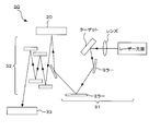
- a pattern transfer apparatus 50 equipped with a reflective mask is roughly composed of a laser plasma X-ray source 31, a reduction optical system 32, and the like.
- the reduction optical system 32 uses an X-ray reflection mirror.
- the pattern reflected by the reflective mask 20 is usually reduced to about 1 ⁇ 4. Since the wavelength band of 13 to 14 nm is used as the exposure wavelength, the optical path was set in advance so as to be in a vacuum.
- EUV light obtained from the laser plasma X-ray source 31 is incident on the reflective mask 20, and the light reflected here passes through the reduction optical system 32 on the silicon wafer (semiconductor substrate with resist layer) 33. Transcribed to.
- the light incident on the reflective mask 20 is absorbed by the absorber film and is not reflected in the portion having the absorber film pattern, while the light incident on the portion without the absorber film pattern is reflected by the multilayer reflective film.
- the exposure light passing through the reduction optical system 32 exposes the transfer pattern on the resist layer on the silicon wafer 33. Then, a resist pattern was formed on the silicon wafer 33 by developing the exposed resist layer.
- the mask contrast of the reflective mask of this example was as high as 1: 1000, and the mask accuracy was 4.8 nm or less, which is the required accuracy of the DRAM hp32nm design rule. It was confirmed that.
- Example 2 A substrate with a multilayer reflective film was produced in the same manner as in Example 1, and a chromium nitride buffer film was formed on the Ru protective film as in Example 1.
- a material containing Ta and N was formed on the buffer film as a lower layer of the absorber film with a thickness of 60 nm. That is, using a Ta target, 10% of nitrogen (N 2 ) was added to argon (Ar), and a film was formed by DC magnetron sputtering. The composition ratio of the formed TaN film was 80 at% for Ta and 20 at% for N.
- a material containing Ta and O was formed to a thickness of 20 nm as the uppermost layer of the absorber film. That is, using a Ta target, 10% of oxygen (O 2 ) was added to argon (Ar), and a film was formed by DC magnetron sputtering. The composition ratio of the formed TaO film was 80 at% for Ta and 20 at% for O.
- the formed TaN film (lower layer) has a refractive index n of 0.9532 and an extinction coefficient k of ⁇ 0.0436, and the formed TaO film (uppermost layer) has a refractive index n of 0.9597 and an extinction coefficient.
- the attenuation coefficient k was -0.0264.
- the transmittance of the uppermost TaO film measured with 13.5 nm EUV light at an incident angle of 6.0 degrees was 0.65%.
- the reflective mask blank of this example was produced as described above.
- Example 2 pattern transfer by EUV light onto the semiconductor substrate by the pattern transfer apparatus shown in FIG. 2 was performed as in Example 1.
- the reflective mask of this example was used.
- the mask contrast was as high as 1: 1000, and it was confirmed that the mask accuracy was 4.8 nm or less, which is the required accuracy of the DRAM hp32 nm design rule.
- Example 3 A substrate with a multilayer reflective film was produced in the same manner as in Example 1, and a chromium nitride buffer film was formed on the Ru protective film as in Example 1.
- a Ta film having a thickness of 50 nm was formed on the buffer film as a lower layer of the absorber film. That is, a film was formed by a DC magnetron sputtering method in an argon gas (Ar) using a Ta target.
- Ar argon gas
- a material containing Ta and O was formed to a thickness of 20 nm as the uppermost layer of the absorber film. That is, using a Ta target, 10% of oxygen (O 2 ) was added to argon (Ar), and a film was formed by DC magnetron sputtering. The composition ratio of the formed TaO film was 80 at% for Ta and 20 at% for O.
- the formed Ta film (lower layer) has a refractive index n of 0.9597 and an extinction coefficient k of -0.0458, and the formed TaO film (upper layer) has a refractive index n of 0.9597 and an extinction coefficient.
- the attenuation coefficient k was -0.0264.
- the transmittance of the uppermost TaO film measured with 13.5 nm EUV light at an incident angle of 6.0 degrees was 0.78%.
- the reflective mask blank of this example was produced as described above.
- Example 2 pattern transfer by EUV light onto the semiconductor substrate by the pattern transfer apparatus shown in FIG. 2 was performed as in Example 1.
- the reflective mask of this example was used.
- the mask contrast was as high as 1: 1000, and it was confirmed that the mask accuracy was 4.8 nm or less, which is the required accuracy of the DRAM hp32 nm design rule.
Landscapes
- Engineering & Computer Science (AREA)
- Physics & Mathematics (AREA)
- Chemical & Material Sciences (AREA)
- Nanotechnology (AREA)
- General Physics & Mathematics (AREA)
- Crystallography & Structural Chemistry (AREA)
- Condensed Matter Physics & Semiconductors (AREA)
- Manufacturing & Machinery (AREA)
- Mathematical Physics (AREA)
- Theoretical Computer Science (AREA)
- Preparing Plates And Mask In Photomechanical Process (AREA)
- Exposure Of Semiconductors, Excluding Electron Or Ion Beam Exposure (AREA)
Abstract
Description
使用する基板は、SiO2-TiO2系のガラス基板(6インチ角、厚さが6.3mm)である。この基板の熱膨張係数は0.2×10⁻⁷/℃、ヤング率は67GPaである。そして、このガラス基板は機械研磨により、0.2nmRms以下の平滑な表面と、50nm以下の平坦度に形成した。
実施例1と同様にして多層反射膜付き基板を作製し、そのRu保護膜上に、実施例1と同じく窒化クロム膜のバッファ膜を形成した。
実施例1と同様にして多層反射膜付き基板を作製し、そのRu保護膜上に、実施例1と同じく窒化クロム膜のバッファ膜を形成した。
2 多層反射膜
3 バッファ膜
4 吸収体膜
4a 下層
4b 最上層
5 レジスト膜
10 反射型マスクブランク
20 反射型マスク
50 パターン転写装置
Claims (4)
- 基板と、該基板上に形成された露光光を反射する多層反射膜と、該多層反射膜上に形成された露光光を吸収する吸収体膜とを有し、EUV光を露光光とするEUVリソグラフィで用いられる反射型マスクブランクであって、
前記吸収体膜は、最上層と、それ以外の下層とからなる積層構造となっており、
前記最上層は、タンタル(Ta)の酸化物、窒化物、酸窒化物、または炭化物のいずれかを含む材料で形成され、屈折率nが0.95~0.97の範囲、消衰係数kが-0.033~-0.023の範囲であり、
前記下層は、タンタル(Ta)を含む材料で形成され、屈折率nが0.94~0.97の範囲、消衰係数kが-0.050~-0.036の範囲であることを特徴とする反射型マスクブランク。 - 前記吸収体膜の下層は、さらにホウ素(B)と窒素(N)のうち少なくとも1以上の元素を含有することを特徴とする、請求項1に記載の反射型マスクブランク。
- 前記多層反射膜と前記吸収体膜との間に、クロム(Cr)の窒化物を含む材料で形成され、屈折率nが0.90~0.95の範囲、消衰係数kが-0.043~-0.030の範囲であるバッファ膜を有することを特徴とする、請求項1又は2に記載の反射型マスクブランク。
- 請求項1乃至3のいずれか一項に記載の反射型マスクブランクの前記吸収体膜に、被転写体に対する転写パターンとなる吸収体膜パターンを形成することを特徴とする、反射型マスクの製造方法。
Priority Applications (2)
| Application Number | Priority Date | Filing Date | Title |
|---|---|---|---|
| US13/122,024 US8389184B2 (en) | 2009-02-04 | 2010-01-29 | Reflective mask blank and method of manufacturing a reflective mask |
| KR1020117003902A KR101676052B1 (ko) | 2009-02-04 | 2010-01-29 | 반사형 마스크 블랭크 및 반사형 마스크의 제조 방법 |
Applications Claiming Priority (4)
| Application Number | Priority Date | Filing Date | Title |
|---|---|---|---|
| JP2009023957 | 2009-02-04 | ||
| JP2009-023957 | 2009-02-04 | ||
| JP2009-115307 | 2009-05-12 | ||
| JP2009115307A JP5638769B2 (ja) | 2009-02-04 | 2009-05-12 | 反射型マスクブランクの製造方法及び反射型マスクの製造方法 |
Publications (1)
| Publication Number | Publication Date |
|---|---|
| WO2010090132A1 true WO2010090132A1 (ja) | 2010-08-12 |
Family
ID=42542029
Family Applications (1)
| Application Number | Title | Priority Date | Filing Date |
|---|---|---|---|
| PCT/JP2010/051204 Ceased WO2010090132A1 (ja) | 2009-02-04 | 2010-01-29 | 反射型マスクブランク及び反射型マスクの製造方法 |
Country Status (5)
| Country | Link |
|---|---|
| US (1) | US8389184B2 (ja) |
| JP (1) | JP5638769B2 (ja) |
| KR (1) | KR101676052B1 (ja) |
| TW (1) | TWI436159B (ja) |
| WO (1) | WO2010090132A1 (ja) |
Cited By (4)
| Publication number | Priority date | Publication date | Assignee | Title |
|---|---|---|---|---|
| JP2015008283A (ja) * | 2013-05-31 | 2015-01-15 | Hoya株式会社 | 反射型マスクブランク、反射型マスク及びその製造方法、並びに半導体装置の製造方法 |
| WO2020241780A1 (ja) * | 2019-05-31 | 2020-12-03 | 凸版印刷株式会社 | 反射型フォトマスクブランクス及び反射型フォトマスク |
| JP2021110952A (ja) * | 2020-01-08 | 2021-08-02 | エスアンドエス テック カンパニー リミテッド | 極紫外線用反射型ブランクマスク及びフォトマスク |
| US11150550B2 (en) | 2017-08-10 | 2021-10-19 | AGC Inc. | Reflective mask blank and reflective mask |
Families Citing this family (15)
| Publication number | Priority date | Publication date | Assignee | Title |
|---|---|---|---|---|
| JP5971122B2 (ja) | 2011-02-01 | 2016-08-17 | 旭硝子株式会社 | Euvリソグラフィ用反射型マスクブランク |
| KR101862166B1 (ko) | 2012-03-14 | 2018-05-29 | 호야 가부시키가이샤 | 마스크 블랭크, 및 전사용 마스크의 제조방법 |
| US20150079502A1 (en) * | 2012-03-14 | 2015-03-19 | Hoya Corporation | Mask blank and method of manufacturing a transfer mask |
| KR101477469B1 (ko) | 2012-03-30 | 2014-12-29 | 호야 가부시키가이샤 | 마스크 블랭크용 기판, 다층 반사막 부착 기판, 투과형 마스크 블랭크, 반사형 마스크 블랭크, 투과형 마스크, 반사형 마스크 및 반도체 장치의 제조 방법 |
| US9046781B2 (en) | 2013-03-15 | 2015-06-02 | Taiwan Semiconductor Manufacturing Company, Ltd. | Structure and method for reflective-type mask |
| JP6340800B2 (ja) * | 2014-01-24 | 2018-06-13 | 凸版印刷株式会社 | Euv露光用マスク及びその製造方法 |
| US9357625B2 (en) * | 2014-07-07 | 2016-05-31 | Asml Netherlands B.V. | Extreme ultraviolet light source |
| US9709884B2 (en) * | 2014-11-26 | 2017-07-18 | Taiwan Semiconductor Manufacturing Company, Ltd. | EUV mask and manufacturing method by using the same |
| US11281088B2 (en) * | 2017-04-17 | 2022-03-22 | AGC Inc. | Reflective mask blank for EUV exposure, and reflective mask |
| US10890842B2 (en) * | 2017-09-21 | 2021-01-12 | AGC Inc. | Reflective mask blank, reflective mask, and process for producing reflective mask blank |
| JP7250511B2 (ja) | 2018-12-27 | 2023-04-03 | Hoya株式会社 | 反射型マスクブランク、反射型マスク、及び半導体装置の製造方法 |
| KR20210126592A (ko) * | 2019-02-28 | 2021-10-20 | 호야 가부시키가이샤 | 반사형 마스크 블랭크, 반사형 마스크 및 그 제조 방법, 그리고 반도체 장치의 제조 방법 |
| KR102898054B1 (ko) * | 2020-04-14 | 2025-12-10 | 삼성전자주식회사 | 극자외선 리소그래피용 위상 반전 마스크 |
| JP7612408B2 (ja) * | 2020-12-22 | 2025-01-14 | Hoya株式会社 | 反射型マスクブランク、反射型マスク、反射型マスクの製造方法、及び半導体デバイスの製造方法 |
| JPWO2024247713A1 (ja) * | 2023-05-31 | 2024-12-05 |
Citations (1)
| Publication number | Priority date | Publication date | Assignee | Title |
|---|---|---|---|---|
| JP2004006798A (ja) * | 2002-04-11 | 2004-01-08 | Hoya Corp | 反射型マスクブランクス及び反射型マスク及びそれらの製造方法並びに半導体の製造方法 |
Family Cites Families (5)
| Publication number | Priority date | Publication date | Assignee | Title |
|---|---|---|---|---|
| JPH08213303A (ja) | 1995-02-03 | 1996-08-20 | Nikon Corp | 反射型x線マスク及びその製造法 |
| US7390596B2 (en) | 2002-04-11 | 2008-06-24 | Hoya Corporation | Reflection type mask blank and reflection type mask and production methods for them |
| JP4946296B2 (ja) * | 2006-03-30 | 2012-06-06 | 凸版印刷株式会社 | 反射型フォトマスクブランク及びその製造方法、反射型フォトマスク、並びに、半導体装置の製造方法 |
| TWI444757B (zh) * | 2006-04-21 | 2014-07-11 | 旭硝子股份有限公司 | 用於極紫外光(euv)微影術之反射性空白光罩 |
| JP5018212B2 (ja) * | 2007-04-26 | 2012-09-05 | 凸版印刷株式会社 | 反射型フォトマスクブランク及び反射型フォトマスク並びに半導体装置の製造方法 |
-
2009
- 2009-05-12 JP JP2009115307A patent/JP5638769B2/ja active Active
-
2010
- 2010-01-29 US US13/122,024 patent/US8389184B2/en active Active
- 2010-01-29 KR KR1020117003902A patent/KR101676052B1/ko active Active
- 2010-01-29 WO PCT/JP2010/051204 patent/WO2010090132A1/ja not_active Ceased
- 2010-02-04 TW TW099103374A patent/TWI436159B/zh active
Patent Citations (1)
| Publication number | Priority date | Publication date | Assignee | Title |
|---|---|---|---|---|
| JP2004006798A (ja) * | 2002-04-11 | 2004-01-08 | Hoya Corp | 反射型マスクブランクス及び反射型マスク及びそれらの製造方法並びに半導体の製造方法 |
Cited By (10)
| Publication number | Priority date | Publication date | Assignee | Title |
|---|---|---|---|---|
| JP2015008283A (ja) * | 2013-05-31 | 2015-01-15 | Hoya株式会社 | 反射型マスクブランク、反射型マスク及びその製造方法、並びに半導体装置の製造方法 |
| US11150550B2 (en) | 2017-08-10 | 2021-10-19 | AGC Inc. | Reflective mask blank and reflective mask |
| US11703751B2 (en) | 2017-08-10 | 2023-07-18 | AGC Inc. | Reflective mask blank and reflective mask |
| WO2020241780A1 (ja) * | 2019-05-31 | 2020-12-03 | 凸版印刷株式会社 | 反射型フォトマスクブランクス及び反射型フォトマスク |
| JP2020197606A (ja) * | 2019-05-31 | 2020-12-10 | 凸版印刷株式会社 | 反射型フォトマスクブランクス及び反射型フォトマスク |
| JP7346088B2 (ja) | 2019-05-31 | 2023-09-19 | 株式会社トッパンフォトマスク | 反射型フォトマスクブランクス及び反射型フォトマスク |
| TWI841741B (zh) * | 2019-05-31 | 2024-05-11 | 日商凸版光掩模有限公司 | 反射型空白光罩及反射型光罩 |
| US12111565B2 (en) | 2019-05-31 | 2024-10-08 | Toppan Inc. | Reflective photomask blank and reflective photomask |
| JP2021110952A (ja) * | 2020-01-08 | 2021-08-02 | エスアンドエス テック カンパニー リミテッド | 極紫外線用反射型ブランクマスク及びフォトマスク |
| US11815801B2 (en) | 2020-01-08 | 2023-11-14 | S & S Tech Co., Ltd. | Reflective type blankmask and photomask for EUV |
Also Published As
| Publication number | Publication date |
|---|---|
| KR20120057551A (ko) | 2012-06-05 |
| JP5638769B2 (ja) | 2014-12-10 |
| TW201102753A (en) | 2011-01-16 |
| US8389184B2 (en) | 2013-03-05 |
| US20110281207A1 (en) | 2011-11-17 |
| KR101676052B1 (ko) | 2016-11-14 |
| JP2010206156A (ja) | 2010-09-16 |
| TWI436159B (zh) | 2014-05-01 |
Similar Documents
| Publication | Publication Date | Title |
|---|---|---|
| JP5638769B2 (ja) | 反射型マスクブランクの製造方法及び反射型マスクの製造方法 | |
| JP5507876B2 (ja) | 反射型マスクブランク及び反射型マスクの製造方法 | |
| JP5974321B2 (ja) | 反射型マスクブランク及び反射型マスクの製造方法 | |
| JP4163038B2 (ja) | 反射型マスクブランク及び反射型マスク並びに半導体の製造方法 | |
| JP2006332153A (ja) | 反射型マスクブランク及び反射型マスク並びに半導体装置の製造方法 | |
| JP5372455B2 (ja) | 反射型マスクブランク及び反射型マスク、並びにこれらの製造方法 | |
| JP4553239B2 (ja) | 反射型マスクブランクス及び反射型マスク並びに半導体装置の製造方法 | |
| JP4926521B2 (ja) | 反射型マスクブランクス及び反射型マスク並びに半導体装置の製造方法 | |
| JP2010109336A (ja) | 反射型マスクの製造方法 | |
| JP2022098729A (ja) | 反射型マスクブランク、反射型マスク、反射型マスクの製造方法、及び半導体デバイスの製造方法 | |
| JP2004363570A (ja) | 反射多層膜付き基板及び反射型マスクブランクス並びに反射型マスク | |
| JP2004281967A (ja) | 反射型マスクブランクス及び反射型マスク | |
| JP4320050B2 (ja) | 反射型マスクブランクス及びその製造方法、反射型マスク | |
| JP4418700B2 (ja) | 反射型マスクブランクス及び反射型マスク並びに半導体装置の製造方法 | |
| JP4541654B2 (ja) | 反射型マスクの製造方法 |
Legal Events
| Date | Code | Title | Description |
|---|---|---|---|
| 121 | Ep: the epo has been informed by wipo that ep was designated in this application |
Ref document number: 10738466 Country of ref document: EP Kind code of ref document: A1 |
|
| ENP | Entry into the national phase |
Ref document number: 20117003902 Country of ref document: KR Kind code of ref document: A |
|
| WWE | Wipo information: entry into national phase |
Ref document number: 13122024 Country of ref document: US |
|
| NENP | Non-entry into the national phase |
Ref country code: DE |
|
| 122 | Ep: pct application non-entry in european phase |
Ref document number: 10738466 Country of ref document: EP Kind code of ref document: A1 |