WO2010089867A1 - 転写装置および転写方法 - Google Patents
転写装置および転写方法 Download PDFInfo
- Publication number
- WO2010089867A1 WO2010089867A1 PCT/JP2009/051950 JP2009051950W WO2010089867A1 WO 2010089867 A1 WO2010089867 A1 WO 2010089867A1 JP 2009051950 W JP2009051950 W JP 2009051950W WO 2010089867 A1 WO2010089867 A1 WO 2010089867A1
- Authority
- WO
- WIPO (PCT)
- Prior art keywords
- mold
- pattern
- transfer
- hole
- substrate
- Prior art date
- Legal status (The legal status is an assumption and is not a legal conclusion. Google has not performed a legal analysis and makes no representation as to the accuracy of the status listed.)
- Ceased
Links
Images





Classifications
-
- G—PHYSICS
- G11—INFORMATION STORAGE
- G11B—INFORMATION STORAGE BASED ON RELATIVE MOVEMENT BETWEEN RECORD CARRIER AND TRANSDUCER
- G11B5/00—Recording by magnetisation or demagnetisation of a record carrier; Reproducing by magnetic means; Record carriers therefor
- G11B5/84—Processes or apparatus specially adapted for manufacturing record carriers
- G11B5/855—Coating only part of a support with a magnetic layer
-
- B—PERFORMING OPERATIONS; TRANSPORTING
- B29—WORKING OF PLASTICS; WORKING OF SUBSTANCES IN A PLASTIC STATE IN GENERAL
- B29C—SHAPING OR JOINING OF PLASTICS; SHAPING OF MATERIAL IN A PLASTIC STATE, NOT OTHERWISE PROVIDED FOR; AFTER-TREATMENT OF THE SHAPED PRODUCTS, e.g. REPAIRING
- B29C35/00—Heating, cooling or curing, e.g. crosslinking or vulcanising; Apparatus therefor
- B29C35/02—Heating or curing, e.g. crosslinking or vulcanizing during moulding, e.g. in a mould
- B29C35/08—Heating or curing, e.g. crosslinking or vulcanizing during moulding, e.g. in a mould by wave energy or particle radiation
- B29C35/0888—Heating or curing, e.g. crosslinking or vulcanizing during moulding, e.g. in a mould by wave energy or particle radiation using transparant moulds
-
- B—PERFORMING OPERATIONS; TRANSPORTING
- B29—WORKING OF PLASTICS; WORKING OF SUBSTANCES IN A PLASTIC STATE IN GENERAL
- B29C—SHAPING OR JOINING OF PLASTICS; SHAPING OF MATERIAL IN A PLASTIC STATE, NOT OTHERWISE PROVIDED FOR; AFTER-TREATMENT OF THE SHAPED PRODUCTS, e.g. REPAIRING
- B29C59/00—Surface shaping of articles, e.g. embossing; Apparatus therefor
- B29C59/02—Surface shaping of articles, e.g. embossing; Apparatus therefor by mechanical means, e.g. pressing
-
- B—PERFORMING OPERATIONS; TRANSPORTING
- B82—NANOTECHNOLOGY
- B82Y—SPECIFIC USES OR APPLICATIONS OF NANOSTRUCTURES; MEASUREMENT OR ANALYSIS OF NANOSTRUCTURES; MANUFACTURE OR TREATMENT OF NANOSTRUCTURES
- B82Y10/00—Nanotechnology for information processing, storage or transmission, e.g. quantum computing or single electron logic
-
- B—PERFORMING OPERATIONS; TRANSPORTING
- B82—NANOTECHNOLOGY
- B82Y—SPECIFIC USES OR APPLICATIONS OF NANOSTRUCTURES; MEASUREMENT OR ANALYSIS OF NANOSTRUCTURES; MANUFACTURE OR TREATMENT OF NANOSTRUCTURES
- B82Y40/00—Manufacture or treatment of nanostructures
-
- G—PHYSICS
- G03—PHOTOGRAPHY; CINEMATOGRAPHY; ANALOGOUS TECHNIQUES USING WAVES OTHER THAN OPTICAL WAVES; ELECTROGRAPHY; HOLOGRAPHY
- G03F—PHOTOMECHANICAL PRODUCTION OF TEXTURED OR PATTERNED SURFACES, e.g. FOR PRINTING, FOR PROCESSING OF SEMICONDUCTOR DEVICES; MATERIALS THEREFOR; ORIGINALS THEREFOR; APPARATUS SPECIALLY ADAPTED THEREFOR
- G03F7/00—Photomechanical, e.g. photolithographic, production of textured or patterned surfaces, e.g. printing surfaces; Materials therefor, e.g. comprising photoresists; Apparatus specially adapted therefor
- G03F7/0002—Lithographic processes using patterning methods other than those involving the exposure to radiation, e.g. by stamping
-
- B—PERFORMING OPERATIONS; TRANSPORTING
- B29—WORKING OF PLASTICS; WORKING OF SUBSTANCES IN A PLASTIC STATE IN GENERAL
- B29C—SHAPING OR JOINING OF PLASTICS; SHAPING OF MATERIAL IN A PLASTIC STATE, NOT OTHERWISE PROVIDED FOR; AFTER-TREATMENT OF THE SHAPED PRODUCTS, e.g. REPAIRING
- B29C35/00—Heating, cooling or curing, e.g. crosslinking or vulcanising; Apparatus therefor
- B29C35/02—Heating or curing, e.g. crosslinking or vulcanizing during moulding, e.g. in a mould
- B29C35/08—Heating or curing, e.g. crosslinking or vulcanizing during moulding, e.g. in a mould by wave energy or particle radiation
- B29C35/0805—Heating or curing, e.g. crosslinking or vulcanizing during moulding, e.g. in a mould by wave energy or particle radiation using electromagnetic radiation
- B29C2035/0827—Heating or curing, e.g. crosslinking or vulcanizing during moulding, e.g. in a mould by wave energy or particle radiation using electromagnetic radiation using UV radiation
-
- B—PERFORMING OPERATIONS; TRANSPORTING
- B29—WORKING OF PLASTICS; WORKING OF SUBSTANCES IN A PLASTIC STATE IN GENERAL
- B29C—SHAPING OR JOINING OF PLASTICS; SHAPING OF MATERIAL IN A PLASTIC STATE, NOT OTHERWISE PROVIDED FOR; AFTER-TREATMENT OF THE SHAPED PRODUCTS, e.g. REPAIRING
- B29C59/00—Surface shaping of articles, e.g. embossing; Apparatus therefor
- B29C59/02—Surface shaping of articles, e.g. embossing; Apparatus therefor by mechanical means, e.g. pressing
- B29C59/022—Surface shaping of articles, e.g. embossing; Apparatus therefor by mechanical means, e.g. pressing characterised by the disposition or the configuration, e.g. dimensions, of the embossments or the shaping tools therefor
- B29C2059/023—Microembossing
Definitions
- the present invention relates to a transfer apparatus and a transfer method for transferring an uneven pattern to a transfer layer such as a nanoimprint apparatus.
- the mold and the substrate may be displaced.
- a fine concavo-convex pattern such as a nanoscale
- the mold is pressed against the substrate with the reference position shifted.
- the vacuum suction is performed not only on the outer peripheral portion of the mold but also on the inner peripheral portion, thereby making it possible to perform stronger suction.
- the present invention has been made in view of the above points, and the problem to be solved by the present invention is that the substrate can be irradiated with UV light evenly in a state where the mold is vacuum-adsorbed on the substrate.
- An example is to provide a simple transfer device and transfer method.
- a transfer device is a transfer device that is irradiated with light through a mold and transfers a pattern of the mold to a transfer layer, A substrate having an adsorption surface for adsorbing a mold and a through-hole formed on the adsorption surface and for vacuum-sucking the mold; A space of a predetermined size communicating with the through hole on the opposite side of the suction surface of the base; Pump means for vacuum suction of the mold through the space and the through hole.
- the transfer method according to the present invention is a transfer method in which the pattern of the mold adsorbed on the adsorption surface of the substrate is transferred to the transfer layer by light irradiation through the mold, An adsorption step of adsorbing the mold to the base via a through hole formed in the base and a space having a predetermined size communicating with the through hole; A proximity step of bringing the mold adsorbed on the substrate close to the transfer layer; An irradiation step of irradiating the transfer layer with light in a state where the mold and the transfer layer are close to each other; It is characterized by having.
- the mold has a pattern surface on which a pattern is formed and a surface to be attracted to the substrate, and the through hole has the pattern formed on the pattern surface. It may be formed at the position of the suction surface that sucks the surface to be suctioned corresponding to a non-position.
- the transfer device has a groove formed at a position of the suction surface that sucks the suction target surface corresponding to a position where the pattern is not formed on the pattern surface and communicates with the through hole. It can be.
- a light irradiation means capable of irradiating the mold with light through the base and the space, and a part of the base and a part of the space forming part are formed so as to transmit light.
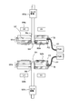
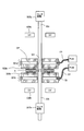
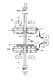
- FIG. 1 It is a schematic block diagram including schematic sectional drawing which shows the nanoimprint apparatus which concerns on embodiment by this invention. It is a schematic sectional drawing which shows typically the principal part of the nanoimprint apparatus for demonstrating the nanoimprint processing method in the nanoimprint apparatus which concerns on embodiment by this invention. It is a schematic sectional drawing which shows typically the principal part of the nanoimprint apparatus for demonstrating the nanoimprint processing method in the nanoimprint apparatus which concerns on embodiment by this invention. It is a schematic sectional drawing which shows typically the principal part of the nanoimprint apparatus for demonstrating the nanoimprint processing method in the nanoimprint apparatus which concerns on embodiment by this invention.
- FIG. 1 is a diagram showing a schematic cross-sectional structure of an ultraviolet irradiation type nanoimprint apparatus that performs pattern transfer based on a nanoimprint method as a transfer apparatus according to the present invention.
- This nanoimprint apparatus uses both an upper mold 503a and a lower mold 503b, each of which has a concavo-convex pattern to be transferred in advance, to perform pattern transfer simultaneously on both sides of a disk-shaped substrate 6 that is a pattern transfer target. It is. On both surfaces of the substrate 6, an upper transfer layer 604a and a lower transfer layer 604b made of a transfer layer material that is cured when irradiated with ultraviolet rays are formed.
- FIG. 1 shows the configuration of the nanoimprint apparatus in a state where the upper transfer layer 604a and the lower transfer layer 604b are formed on the substrate 6.
- the nanoimprint apparatus shown in FIG. 1 includes an upper mechanism unit, a lower mechanism unit, a controller 200 that controls the upper mechanism unit and the lower mechanism unit, and an operation unit 201.
- the upper mechanism unit includes an upper center pin 30a, an upper mold holding unit 501a, an upper stage 505a, an upper center pin driving unit 507a, and an upper ultraviolet irradiation unit 508a.
- the board-like upper stage 505a is provided with an opening 100a penetrating therethrough as shown in FIG. 1, and there is a nut portion around which a screw groove into which a screw portion of a ball screw 512 described later is screwed is cut.
- the upper center pin drive unit 507a and the upper ultraviolet irradiation unit 508a are installed on the opening 100a on the upper surface of the upper stage 505a.
- the upper center pin drive unit 507a supports the upper center pin 30a so that it can be moved up and down by being arranged at the center of the opening 100a.
- an upper mold holding portion 501a made of a transparent material is installed so as to cover the opening 100a.
- the upper mold holding unit 501a includes a mold holding surface (a surface with which the upper mold 503a is in contact in FIG. 1) for fixing and holding the upper mold 503a.
- the upper mold holding portion 501a has a central portion coaxial with the upper mold 503a for supporting the upper center pin 30a in a vertically movable state in a direction perpendicular to the mold holding surface of the upper mold holding portion 501a.
- a through hole is provided as much as possible.
- the upper center pin drive unit 507a moves the upper center pin 30a in a direction perpendicular to the mold holding surface of the upper mold holding portion 501a, that is, the upper center pin. Move upward or downward in the direction of the central axis of 30a.
- the upper ultraviolet irradiation unit 508a around the upper center pin 30a transmits the ultraviolet rays that should cure the transfer layer material via the opening 100a and the upper mold holding unit 501a according to the ultraviolet irradiation signal UV supplied from the controller 200. Then, the light is irradiated toward the upper transfer layer 604a of the substrate 6.
- the camera unit can be provided on the upper surface of the upper stage 505a.
- the reference position alignment of both molds with respect to the substrate 6 can be performed with high accuracy by optically capturing the uneven pattern series formed in each of the upper mold 503a and the lower mold 503b.
- the upper mold holding unit 501a drives the vacuum pump PUM in the suction mechanism (described later) in accordance with the upper mold holding signal MHU supplied from the controller 200 to hold the upper mold 503a in the mold by, for example, vacuum suction. Hold fixed on the surface.
- the lower mechanism part of the nanoimprint apparatus includes a lower center pin 30b, a lower mold holding part 501b, a lower stage 505b, a lower center pin drive unit 507b, a lower ultraviolet irradiation unit 508b, a stage vertical drive unit 511, and a ball screw 512. Is provided.
- the board-like lower stage 505b has a hole through which the threaded portion of the ball screw 512 passes, as well as the opening 100b, as shown in FIG.
- the ball screw 512 maintains the parallel state between the lower stage 505b and the upper stage 505a.
- the screw portion of the ball screw 512 is screwed into the nut portion of the upper stage 505a.
- the lower center pin drive unit 507b and the lower ultraviolet irradiation unit 508b are installed below the opening 100b on the lower surface of the lower stage 505b.
- the lower center pin drive unit 507b supports the lower center pin 30b so that it can be moved up and down by being arranged at the center of the opening 100b.
- the lower center pin 30b is supported so as to be coaxial with the upper center pin 30a.
- the stage vertical drive unit 511 maintains the upper stage 505a parallel to the lower stage 505b by rotating the ball screw 512 clockwise or counterclockwise according to the stage drive signal SG supplied from the controller 200. Move it up or down. That is, the upward movement of the upper stage 505a causes the upper mold holding portion 501a to move away from the lower mold holding portion 501b in the direction perpendicular to the mold holding surface of the lower mold holding portion 501b. To do. On the other hand, the upper mold holding part 501a moves toward the lower mold holding part 501b by the downward movement of the upper stage 505a.
- a lower mold holding portion 501b made of a transparent material is installed so as to cover the opening 100b.
- the lower mold holding part 501b includes a mold holding surface (a surface with which the lower mold 503b is in contact in FIG. 1) for fixing and holding the lower mold 503b.
- a lower mold 503b for supporting the lower center pin 30b in a state of being vertically movable in a direction perpendicular to the mold holding surface of the lower mold holding portion 501b is provided at the center of the lower stage 505b.
- a through hole is provided as coaxial as possible. Therefore, the lower mold 503b is supported so as to be coaxial with the upper mold 503a.
- the lower mold holding unit 501b drives a vacuum pump PUM in an adsorption mechanism (described later) in accordance with a lower mold holding signal MHL supplied from the controller 200, so that the lower mold 503b is moved to its mold holding surface by, for example, vacuum adsorption. Hold fixed to.
- the lower ultraviolet irradiation unit 508b transmits ultraviolet light to be cured from the transfer layer material in accordance with the ultraviolet irradiation signal UV supplied from the controller 200 via the opening 100b and the upper mold holding unit 501b. Irradiation is performed toward the side transfer layer 604b.
- the lower center pin drive unit 507b moves the lower center pin 30b in a direction perpendicular to the mold holding surface of the lower mold holding portion 501b. In other words, the lower center pin 30b is moved upward or downward in the central axis direction.
- the operation unit 201 accepts various operation commands instructed by the user to operate the nanoimprint apparatus, and supplies an operation command signal indicating the operation command to the controller 200.
- the controller 200 generates various control signals for controlling the nanoimprint apparatus by executing a processing program corresponding to the operation indicated by the operation command signal supplied from the operation unit 201.
- the controller 200 starts executing the nanoimprint processing program.
- FIG. 2 shows an initial state, that is, a state where the upper stage 505a is separated from the lower mold holding part 501b by a predetermined distance.
- the upper center pin 30a and the lower center pin 30b are substantially accommodated on the upper mold holding part 501a and the lower mold holding part 501b side, respectively.
- the upper mold 503a and the lower mold 503b carried in by a mold conveying device are sequentially transferred to the upper mold holding part 501a and the lower mold holding part 501b.
- the upper mold holding part 501a and the lower mold holding part 501b adsorb and fix the upper mold 503a and the lower mold 503b by an adsorption mechanism described later.
- the mold conveying device passes the center holes of the lower mold 503b and the upper mold 503a to the upper side so as to penetrate the center pins in the through center holes SH of the upper mold holding part 501a and the lower mold holding part 501b.
- the mold is mounted so as to be coaxial with the mold holding part 501a and the lower mold holding part 501b.
- the lower center pin 30b is raised from the lower stage to a predetermined position, and the substrate 6 is lowered by the center hole of the substrate 6 by the substrate transfer device (not shown). It is attached to 30b.
- a transfer layer is coated on both surfaces of the substrate 6 in advance.
- the lower center pin 30b is lowered until the substrate 6 contacts the lower mold holding portion 501b, and the upper center pin 30a and the upper mold holding portion 501a are also moved downward.
- the stage is driven and moved until the upper mold 503 a contacts the substrate 6.
- a predetermined mold pressing process such as pressurization for pressing the upper mold 503a and the lower mold 503b against the substrate 6 is performed. Since the upper and lower transfer layers are in a liquid state (flowable state), they are deformed along the concavo-convex pattern shape formed in the upper mold 503a and the lower mold 503b, respectively.
- the upper ultraviolet irradiation unit 508a and the lower ultraviolet irradiation unit 508b irradiate the upper and lower transfer layers of the substrate 6 with ultraviolet rays to cure the transfer layer material.
- the upper center pin 30a is left on the substrate 6, the upper stage is moved upward by a predetermined distance from the lower stage, and the upper mold 503a is released from the upper transfer layer of the substrate 6. To do.
- the substrate 6 is released from the lower mold 503b by moving the lower center pin 30b upward.
- the substrate 6 may be fixed by another means so that the substrate 6 does not adhere to the upper mold 503a and move together with the upward movement of the upper stage 505a.
- the upper stage 505a and the lower center pin 30b may be moved simultaneously.
- the upper mold 503a and the lower mold 503b can be released from the substrate 6 at the same time by making the rising speed of the upper stage 505a faster than the rising speed of the lower center pin 30b.
- a concavo-convex pattern in which the concavo-convex state is reversed from the concavo-convex pattern formed in the upper mold 503a is formed on the surface portion of the upper transfer layer 604a.
- a concavo-convex pattern in which the concavo-convex state is reversed from the concavo-convex pattern formed in the lower mold 503b is formed on the surface portion of the lower transfer layer 604b. Thereafter, the substrate 6 is transported by the transport device.
- the upper mold holding portion 501a is fixed and held in a state where the reference position of the upper mold 503a is aligned with the central axis of the lower center pin 30b, and then the upper mold holding portion.
- the upper mold 503a is once detached from the lower center pin 30b.
- the lower mold holding portion 501b is fixed and held in a state where the reference position of the lower mold 503b is matched with the central axis of the lower center pin 30b.
- the substrate 6 is mounted on the lower center pin 30b, and the upper mold holding portion 501a is moved to the center of the lower center pin 30b while maintaining the respective reference positions aligned with the central axis of the lower center pin 30b.
- Both molds are pressed against both surfaces of the substrate 6 by moving toward the lower mold 503b in the axial direction.
- the pressing operation is performed as described above with the reference positions of the substrate 6, the upper mold 503a, and the lower mold 503b being fixed.
- the substrate 6, the upper mold 503a, and the lower mold 503b are “ Even if “deflection” occurs, the respective reference positions are not shifted, and high-precision pattern transfer can be performed. Further, as described above, the mold and the substrate are not displaced during the pressing operation and the releasing operation.
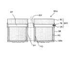
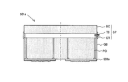
- FIG. 8 is a cross-sectional view of the upper mold holding part 501a adsorbing the upper mold 503a for explaining the adsorption mechanism of the nanoimprint apparatus.
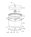
- FIG. 9 is an exploded perspective view of the upper mold holding unit 501a for explaining the suction mechanism of the nanoimprint apparatus.
- FIG. 10 is a perspective view of the base GB for explaining the suction surface FF of the base GB of the upper mold holding portion 501a, and FIG. 9 is viewed from the upside down.
- the upper mold holding portion 501 a is a cylindrical body as a whole having a through center hole SH, and includes a space-forming portion BPF on the back side and a front side ( And a transparent cylindrical substrate GB made of glass or the like fixed to the adsorption surface. Both surfaces (suction surface and back surface plane) of the base GB are polished in parallel with each other.
- the space forming part BPF is composed of a transparent disc-like back flat plate BC made of glass or the like, and external and internal sealing rings CR and ICR made of metal such as SUS fitted therein. Both surfaces (front and back) of the back plate BC are polished in parallel with each other.
- the outer and inner sealing rings CR and ICR define a buffer space SP by airtightly and coaxially joining the columnar base GB (on the back plane BF side) and the back plate BC.
- the external sealing ring CR is provided with a connecting tube TB for connecting the buffer space SP to the external vacuum pump PUM.
- a plurality of through holes PO for adsorbing the upper mold 503a under reduced pressure are formed in parallel to the through center hole SH.
- the through hole PO penetrates from the back plane BF of the base GB to the suction surface FF, and communicates with the buffer space SP extending in the horizontal direction.
- the upper mold holding part 501a includes the transparent base GB having the suction surface FF that sucks the upper mold 503a and the through-hole PO formed in the suction surface FF so as to extend in the normal direction of the suction surface. And a space forming part BPF which forms a buffer space SP of a predetermined size on the back surface BF opposite to the suction surface FF of the base GB and communicates with the through hole PO.
- the connecting pipe TB is connected to the vacuum pump PUM via a flexible pipe FP.
- the vacuum pump PUM is provided with a valve, the vacuum pump PUM is connected to the controller 200, and the vacuum pump and valve are controlled by the controller 200. Therefore, the through-hole PO is connected to the vacuum pump PUM (pump means) through the buffer space SP, the connection pipe TB, and the pipe FP formed by the space forming portion BPF, and thereby the upper mold 503a can be vacuum-sucked. .
- the upper mold 503a has a pattern surface PTT and a surface to be attracted SUF that is attracted to the base GB.
- the pattern surface PTT around the center hole CH includes a pattern region PTTa in which a transfer pattern is formed and a non-pattern region PTTb in which no transfer pattern is formed.
- the through-hole PO is arranged and formed so as to suck a region corresponding to a non-pattern region on the back side of the pattern surface PPT (surface to be attracted SUF) where no pattern is formed. Yes.
- suction grooves GV communicating with the plurality of through holes PO are provided.
- the suction groove GV is formed so as to be in contact with a region corresponding to the non-pattern region on the back side (sucked surface SUF) of the pattern surface PPT when the pattern surface PPT is suctioned to the suction surface FF.
- the upper mold 503a can be irradiated with ultraviolet light through the base GB and the buffer space SP.
- a part of the base GB on which the pattern is formed and a part of the space forming part BPF are formed so as to transmit light.
- a pressure sensor for measuring the pressure in the pipe FP may be provided in the buffer space SP and the pipe FP, and the pressure sensor may be connected to the controller 200.
- the space formation part BPF showed the example comprised from the back surface flat plate BC exterior and the internal sealing rings CR and ICR, you may integrally form these by the base
- the buffer space SP is formed inside the base GB, and the space forming part BPF has a function of members corresponding to the outside of the back flat plate BC and the internal sealing rings CR and ICR being part of the base GB. It becomes.
- the controller 200 drives the vacuum pump PUM and opens the valve of the vacuum pump, thereby evacuating the through hole PO and the pipe FP of the upper mold holding portion 501a, and sucking the upper and lower molds 503a and 503b under reduced pressure.
- the controller 200 controls switching between reduced-pressure adsorption and reduced-pressure adsorption according to the pressure (vacuum degree) in the buffer space SP, the controller 200 performs pressure control when receiving and releasing the upper and lower molds 503a and 503b. It is like that. For example, when removing the upper mold 503a from the upper mold holding part 501a, the upper mold 503a attached to the upper mold holding part 501a is removed by sending air through the pipe FP and the through hole PO by an air delivery device (not shown). Can be made easier.
- the upper mold 503a and the lower center pin 30b are used to hold the substrate 6.
- the through-holes SH are not necessarily required in the cylindrical base GB.
- the suction mechanism of the nano-imprint apparatus of the upper mold holding part 501a or the lower mold holding part 501b in which there is no through center hole for the upper mold 503a and the lower center pin 30b is also included in the present invention.
- the cylindrical base GB and the back flat plate BC have no through center hole, no internal sealing ring, and an external seal provided with a connecting tube TB for connecting the buffer space SP to the PUM.
- the cylindrical base GB and the rear flat plate BC are hermetically and coaxially joined to each other by the stop ring CR to define the buffer space SP.
- the imprint process can be applied to a process for manufacturing a magnetic recording medium such as a discrete track medium or a bit patterned medium.
- an upper mold 503a and a lower mold 503b having desired uneven patterns on the surface of a base material made of quartz glass or the like are manufactured.
- the concavo-convex pattern is formed by forming a resist pattern on a substrate using, for example, an electron beam drawing apparatus, and then performing a dry etching process or the like using the resist pattern as a mask.
- the completed upper mold 503a and lower mold 503b may be subjected to a release treatment or the like for improving the release property.
- quartz glass or the like replicated by the nanoimprint method may be used as a transfer mold using the upper mold 503a and the lower mold 503b as masters. Further, quartz glass or the like replicated by the nanoimprint method from the replica produced by the above method may be used as a transfer mold.
- a magnetic disk media substrate (hereinafter referred to as a media substrate) 600 is manufactured.
- the media substrate 600 has, for example, an upper side on one side (upper side) and the other side (lower side) of a disc-shaped support substrate 601 made of specially processed chemically strengthened glass, silicon wafer, aluminum substrate, or the like.
- a plurality of layers including the transfer layer 604a and the lower transfer layer 604b are laminated as follows.
- an upper nonmagnetic layer 602a made of a nonmagnetic material, an upper metal layer 603a made of a metal material such as tantalum Ta or titanium Ti, and the like An upper transfer layer 604a is laminated.
- a lower nonmagnetic layer 602b made of a nonmagnetic material, a lower metal layer 603b made of a metal material such as Ta or Ti, and a lower transfer layer 604b are stacked on the lower surface of the support substrate 601.
- the upper nonmagnetic layer 602a, the upper metal layer 603a, the lower nonmagnetic layer 602b, and the lower metal layer 603b are formed by a sputtering method or the like.
- the concavo-convex pattern formed on the upper mold 503a and the lower mold 503b is transferred to the upper transfer layer 604a and the lower transfer layer 604b formed on the media substrate 600 by the nanoimprint method described above. That is, the upper transfer layer 604a and the lower transfer layer 604b are formed on the media substrate 600 prepared in the above process by spin coating or the like, and the reference positions of the upper mold 503a and the lower mold 503b are aligned with the center axis of the center pin 30b.
- the media substrate 600 is mounted on the center pin 30b, and the upper mold 503a is placed on the lower mold in the direction of the center axis of the center pin 30b with the reference position aligned with the center axis of the center pin 30b.
- the upper mold 503a is pressed against one surface of the media substrate 600 and the lower mold 503b is pressed against the other surface of the media substrate 600.
- the upper ultraviolet irradiation unit 508a irradiates the upper transfer layer 604a of the media substrate 600 with ultraviolet rays to cure the transfer layer
- the lower ultraviolet irradiation unit 508b emits ultraviolet rays to cure the transfer layer.
- the upper mold 503a and the lower mold 503b are released from the media substrate 600, and the media substrate 600 is taken out.
- a medium substrate 600 having a cross-sectional structure is formed on both sides as shown in FIG.
- etching is performed on both surfaces of the media substrate 600 having a structure.
- the etching process first, the remaining film of the upper transfer layer 604a remains in the portion corresponding to the convex portion of the upper mold 503a, and the residual film of the lower transfer layer 604b remains in the portion corresponding to the convex portion of the lower mold 503b.
- the remaining film is removed by oxygen reactive ion etching (RIE) or the like.
- RIE oxygen reactive ion etching
- the upper metal layer 603a and the lower metal layer 603b are etched and patterned by dry etching using the upper transfer layer 604a and the lower transfer layer 604b patterned by the imprint process as masks.
- the recesses in the concavo-convex patterns of the upper resist layer 604a and the lower resist layer 604b, and the recesses in the upper metal layer 603a and the lower metal layer 603b, respectively. are removed, and a pattern is formed on each of the upper metal layer 603a and the lower metal layer 603b (metal mask patterning step).
- the transfer layer removal process is performed on the both surfaces of the media substrate 600 in a state as shown in FIG. 12B by a method such as wet etching or dry ashing process, and the process shown in FIG. As described above, the transfer layer remaining on each of the upper metal layer 603a and the lower metal layer 603b is removed (transfer layer removing process).
- the non-magnetic material is etched and patterned by dry etching using the upper metal layer 603a and the lower metal layer 603b as a mask with respect to the media substrate 600 in a state as shown in FIG.
- a pattern is formed on the nonmagnetic material by a predetermined depth with respect to the exposed regions of the upper nonmagnetic layer 602a and the lower nonmagnetic layer 602b (not shown). Magnetic layer patterning process).
- the remaining upper metal layer 603a and lower metal layer 603b are removed from both surfaces of the media substrate 600 in a state as shown in FIG. 12D by a method such as wet etching treatment or dry etching treatment.
- a method such as wet etching treatment or dry etching treatment.
- the metal layer remaining in each of the upper nonmagnetic layer 602a and the lower nonmagnetic layer 602b is removed (metal mask removal process).
- the concave portions of the upper nonmagnetic layer 602a and the lower nonmagnetic layer 602b are filled with a magnetic material (shown in black), and further, the upper protective layer 605a and the upper lubricating layer are filled.
- the layer 606a, the lower protective layer 605b, and the lower lubricating layer 606b are stacked as shown in FIG.
- the substrate 6 having the concavo-convex pattern formed on both surfaces thereof by the nanoimprint apparatus shown in FIG. 1 is processed as shown in FIGS. 12A to 12F, so that FIG.
- a double-sided magnetic disk having a cross-sectional structure is manufactured.
- a method of manufacturing a magnetic disk from a media substrate 600 provided with an upper nonmagnetic layer 602a and a lower nonmagnetic layer 602b as shown in FIG. 12A a method of manufacturing a magnetic disk from a media substrate 600 provided with an upper nonmagnetic layer 602a and a lower nonmagnetic layer 602b as shown in FIG. 12A.
- a magnetic disk may be manufactured from the media substrate 600 employing the upper magnetic layer and the lower magnetic layer made of a magnetic material.
- the magnetic material is etched by dry etching using the upper metal layer 603a and the lower metal layer 603b as a mask with respect to the media substrate 600 in a state as shown in FIG.
- a pattern is formed on the magnetic material by a predetermined depth for each exposed region of the lower nonmagnetic layer (magnetic layer patterning step). Then, the magnetic disk is obtained by filling the concave portions of the upper magnetic layer and the lower magnetic layer with a nonmagnetic material.
Landscapes
- Engineering & Computer Science (AREA)
- Nanotechnology (AREA)
- Physics & Mathematics (AREA)
- Chemical & Material Sciences (AREA)
- General Physics & Mathematics (AREA)
- Health & Medical Sciences (AREA)
- Crystallography & Structural Chemistry (AREA)
- Mathematical Physics (AREA)
- Manufacturing & Machinery (AREA)
- Theoretical Computer Science (AREA)
- Mechanical Engineering (AREA)
- Condensed Matter Physics & Semiconductors (AREA)
- Toxicology (AREA)
- Oral & Maxillofacial Surgery (AREA)
- Thermal Sciences (AREA)
- Shaping Of Tube Ends By Bending Or Straightening (AREA)
- Manufacturing Of Magnetic Record Carriers (AREA)
- Exposure Of Semiconductors, Excluding Electron Or Ion Beam Exposure (AREA)
Abstract
転写装置は、モールドを介して光照射がなされ該モールドのパターンを転写層へ転写する転写装置であって、モールドを吸着させる吸着面と吸着面に形成されかつ該モールドを真空吸引する貫通孔とを有し少なくとも一部が光を透過可能な基体と、基体の吸着面の反対側に、貫通孔に連通する所定の大きさの空間と、空間と貫通孔とを介してモールドを真空吸引させるポンプ手段と、を有する。
Description
本発明は、ナノインプリント装置などの転写層に凹凸パターンを転写する転写装置および転写方法に関する。
現在、磁気ディスクの基板に、凹凸状の微細パターンが表面上に形成されているモールドを、転写層が形成された基板に押圧することにより、この凹凸状パターンを基板表面に転写する転写装置が提案されている(例えば、特許文献1の図1参照)。かかる転写装置では、先ず、互いに離間した状態でモールドおよび基板各々の基準位置同士を一致させてから、このモールドを基板の表面に押しつけるようにしている。
ところが、モールドを基板に押圧する際、または離型する際にモールドと基板とがずれてしまう場合があった。特に、ナノスケールのように微細な凹凸状パターンを、表裏2つのモールドを用いて基板の両面に同時に転写する場合に、基準位置がずれた状態でモールドを基板に押しつけてしまう。これにより、裏表の凹凸状パターンが正しく転写された両面磁気ディスクを提供できないという問題が生じる。そこで、モールドを保持する基体にモールドを真空ポンプで真空吸着させる手法がある。この場合、モールドの外周部分のみならず、内周部分でも真空吸着を行うことで、より強固な吸着が可能となるが、基体と真空ポンプとをつなぐ配管や、基体に設けられた配管のうち、特にモールドの内周部分を吸着するためのものが、基板の転写層へのパターン転写時に照射されるUV光等を遮るため、基板に照射されるUV光にムラが生じるという課題があった。
特表2005-529436号公報
そこで、本発明は、上述した点に鑑みてなされたものであって、本発明の解決しようとする課題には、基体にモールドを真空吸着させた状態で、基板にUV光をムラなく照射可能な転写装置および転写方法を提供することが一例として挙げられる。
本発明による転写装置は、モールドを介して光照射がなされ該モールドのパターンを転写層へ転写する転写装置であって、
モールドを吸着させる吸着面と前記吸着面に形成されかつ該モールドを真空吸引する貫通孔とを有し少なくとも一部が前記光を透過可能な基体と、
前記基体の前記吸着面の反対側に、前記貫通孔に連通する所定の大きさの空間と、
前記空間と前記貫通孔とを介して前記モールドを真空吸引させるポンプ手段と、を有することを特徴とする。
本発明による転写方法は、モールドを介して光照射することで、基体の吸着面に吸着された該モールドのパターンを転写層へ転写する転写方法であって、
前記基体に形成された貫通孔及び、前記貫通孔に連通する所定の大きさの空間とを介して前記基体に前記モールドを吸着させる吸着工程と、
前記基体に吸着された前記モールドを、前記転写層に近接させる近接工程と、
前記モールドと前記転写層とが近接した状態で、前記転写層に光照射する照射工程と、
を有することを特徴とする。
モールドを吸着させる吸着面と前記吸着面に形成されかつ該モールドを真空吸引する貫通孔とを有し少なくとも一部が前記光を透過可能な基体と、
前記基体の前記吸着面の反対側に、前記貫通孔に連通する所定の大きさの空間と、
前記空間と前記貫通孔とを介して前記モールドを真空吸引させるポンプ手段と、を有することを特徴とする。
本発明による転写方法は、モールドを介して光照射することで、基体の吸着面に吸着された該モールドのパターンを転写層へ転写する転写方法であって、
前記基体に形成された貫通孔及び、前記貫通孔に連通する所定の大きさの空間とを介して前記基体に前記モールドを吸着させる吸着工程と、
前記基体に吸着された前記モールドを、前記転写層に近接させる近接工程と、
前記モールドと前記転写層とが近接した状態で、前記転写層に光照射する照射工程と、
を有することを特徴とする。
本発明による転写装置においては、前記モールドは、パターンが形成されたパターン面と前記基体に吸着される被吸着面とを有し、前記貫通孔は、前記パターン面のうち前記パターンが形成されていない位置に対応する前記被吸着面を吸引する前記吸着面の位置に形成されていることとすることができる。
本発明による転写装置においては、前記パターン面のうち前記パターンが形成されていない位置に対応する前記被吸着面を吸引する前記吸着面の位置に形成されかつ前記貫通孔に連通する溝を有することとすることができる。
本発明による転写装置においては、前記基体および前記空間を介して前記モールドに光を照射可能な光照射手段を有し、前記基体の一部および空間形成部の一部は光を透過可能に形成されていることとすることができる。
6 基板
30a 上側センターピン
30b 下側センターピン
100a 開口部
100b 開口部
200 コントローラ
201 操作部
501a 上側モールド保持部
501b 下側モールド保持部
503a 上側モールド
503b 下側モールド
505a 上側ステージ
505b 下側ステージ
507a 上側センターピン駆動ユニット
507b 下側センターピン駆動ユニット
508a 上側紫外線照射ユニット
508b 下側紫外線照射ユニット
511 ステージ上下駆動ユニット
512 ボールネジ
600 メディア基板
601 支持基板
602a 上側非磁性層
603a 上側メタル層
602b 下側非磁性層
603b 下側メタル層
604a 上側転写層
604b 下側転写層
CGU 上側センターピン移動信号
CGL 下側センターピン移動信号
UV 紫外線照射信号
MHU 上側モールド保持信号
MHL 下側モールド保持信号
SG ステージ駆動信号
SH 貫通中心孔
BPF 空間形成部
GB 基体
BC 背面平板
CR 外部封止リング
ICR 内部封止リング
SP バッファ空間
CR 外部封止リング
PUM 真空ポンプ
TB 接続管
PO 貫通孔
BF 背面平面
SUF 被吸着面
PTT パターン面
GV 吸着溝
30a 上側センターピン
30b 下側センターピン
100a 開口部
100b 開口部
200 コントローラ
201 操作部
501a 上側モールド保持部
501b 下側モールド保持部
503a 上側モールド
503b 下側モールド
505a 上側ステージ
505b 下側ステージ
507a 上側センターピン駆動ユニット
507b 下側センターピン駆動ユニット
508a 上側紫外線照射ユニット
508b 下側紫外線照射ユニット
511 ステージ上下駆動ユニット
512 ボールネジ
600 メディア基板
601 支持基板
602a 上側非磁性層
603a 上側メタル層
602b 下側非磁性層
603b 下側メタル層
604a 上側転写層
604b 下側転写層
CGU 上側センターピン移動信号
CGL 下側センターピン移動信号
UV 紫外線照射信号
MHU 上側モールド保持信号
MHL 下側モールド保持信号
SG ステージ駆動信号
SH 貫通中心孔
BPF 空間形成部
GB 基体
BC 背面平板
CR 外部封止リング
ICR 内部封止リング
SP バッファ空間
CR 外部封止リング
PUM 真空ポンプ
TB 接続管
PO 貫通孔
BF 背面平面
SUF 被吸着面
PTT パターン面
GV 吸着溝
以下に本発明の実施の形態を図面を参照しつつ説明する。
<ナノインプリント装置>
図1は、本発明による転写装置としてナノインプリント方法に基づきパターン転写を行う、紫外線照射式のナノインプリント装置の概略断面構造を示す図である。
図1は、本発明による転写装置としてナノインプリント方法に基づきパターン転写を行う、紫外線照射式のナノインプリント装置の概略断面構造を示す図である。
このナノインプリント装置は、それぞれ転写すべき凹凸パターンが予め形成されている上側モールド503aおよび下側モールド503bを用いて、パターンの転写対象となるディスク状の基板6に対して両面同時にパターン転写を行うものである。基板6の両面には、紫外線が照射されると硬化する転写層材料からなる上側転写層604aおよび下側転写層604bが形成されている。尚、図1には、これら基板6に上側転写層604aおよび下側転写層604bが形成された状態で、ナノインプリント装置の構成を示している。
図1に示すナノインプリント装置は、上側機構部、下側機構部、これら上側機構部および下側機構部を制御するコントローラ200および操作部201から構成される。
上側機構部は、上側センターピン30a、上側モールド保持部501a、上側ステージ505a、上側センターピン駆動ユニット507a、上側紫外線照射ユニット508aを備える。
ボード状の上側ステージ505aには、図1に示すように貫通する開口部100aが設けられ、その周りに後述するボールネジ512のネジ部がねじ込まれるネジ溝が切られているナット部が存在する。
上側ステージ505aの上面の開口部100a上には、上側センターピン駆動ユニット507a、上側紫外線照射ユニット508aの各ユニットが設置されている。上側センターピン駆動ユニット507aは上側センターピン30aが開口部100aの中心に配置され上下移動可能な状態となるように支持している。
上側ステージ505aの下面には、その開口部100aを覆うように透明材料からなる上側モールド保持部501aが設置されている。上側モールド保持部501aは、上側モールド503aを固定保持させるためのモールド保持面(図1において上側モールド503aが接触している面)を備えている。また、上側モールド保持部501aの中心部には、上側センターピン30aを上側モールド保持部501aのモールド保持面に対して垂直な方向において上下移動可能な状態で支持するための上側モールド503aと同軸となるべく貫通孔が設けられている。
上側センターピン駆動ユニット507aは、コントローラ200から供給された上側センターピン移動信号CGUに応じて、上側センターピン30aを、上側モールド保持部501aのモールド保持面に対して垂直な方向、つまり上側センターピン30aの中心軸方向において上側または下側に移動させる。上側センターピン30aまわりにある上側紫外線照射ユニット508aは、コントローラ200から供給された紫外線照射信号UVに応じて、転写層材料を硬化させるべき紫外線を、上記開口部100aおよび上側モールド保持部501aを介して、基板6の上側転写層604aに向けて照射する。
なお、図示しないがカメラユニットを上側ステージ505aの上面などに設けることができる。これにより、上側モールド503aおよび下側モールド503b各々に形成されている凹凸パターン系列を光学的に捉えることによって、基板6に対して両モールドの基準位置合わせを高精度に実施することができる。
上側モールド保持部501aは、コントローラ200から供給された上側モールド保持信号MHUに応じて吸着機構(後述する)における真空ホンプPUMを駆動して例えば真空吸着することにより、この上側モールド503aをそのモールド保持面に固定保持する。
ナノインプリント装置の下側機構部は、下側センターピン30b、下側モールド保持部501b、下側ステージ505b、下側センターピン駆動ユニット507b、下側紫外線照射ユニット508b、ステージ上下駆動ユニット511およびボールネジ512を備える。
ボード状の下側ステージ505bには、図1に示すように開口部100bと共に、ボールネジ512のネジ部が貫通する穴部が存在する。ボールネジ512は、下側ステージ505bおよび上側ステージ505aによる互いの平行状態を維持させる。ボールネジ512のネジ部は上側ステージ505aのナット部にネジ込まれている。
下側ステージ505bの下面の開口部100b下には、下側センターピン駆動ユニット507bおよび下側紫外線照射ユニット508bの各ユニットが設置されている。下側センターピン駆動ユニット507bは下側センターピン30bが開口部100bの中心に配置され上下移動可能な状態となるように支持している。
下側センターピン30bは上側センターピン30aと同軸となるように支持されている。
ステージ上下駆動ユニット511は、コントローラ200から供給されたステージ駆動信号SGに応じて、ボールネジ512を時計方向または反時計方向に回転させることにより、上側ステージ505aを、下側ステージ505bに対する平行状態を維持したまま上方向または下方向に移動させる。すなわち、上側ステージ505aの上方向への移動により、上側モールド保持部501aが、下側モールド保持部501bのモールド保持面に対して垂直な方向においてこの下側モールド保持部501bから離間するように移動する。一方、上側ステージ505aの下方向への移動により、上側モールド保持部501aが、下側モールド保持部501bに向けて移動する。
下側ステージ505bの上面には、その開口部100bを覆うように透明材料からなる下側モールド保持部501bが設置されている。下側モールド保持部501bは、下側モールド503bを固定保持させるためのモールド保持面(図1において下側モールド503bが接触している面)を備えている。また、下側ステージ505bの中心部には、下側センターピン30bを下側モールド保持部501bのモールド保持面に対して垂直な方向において上下移動可能な状態で支持するための下側モールド503bと同軸となるべく貫通孔が設けられている。よって、下側モールド503bは上側モールド503aと同軸となるように支持される。
下側モールド保持部501bは、コントローラ200から供給された下側モールド保持信号MHLに応じて吸着機構(後述する)における真空ホンプPUMを駆動して例えば真空吸着によって下側モールド503bをそのモールド保持面に固定保持する。
下側紫外線照射ユニット508bは、コントローラ200から供給された紫外線照射信号UVに応じて、転写層材料を硬化させるべき紫外線を、上記開口部100bおよび上側モールド保持部501bを介して、基板6の下側転写層604bに向けて照射する。
下側センターピン駆動ユニット507bは、コントローラ200から供給された下側センターピン移動信号CGLに応じて、下側センターピン30bを、下側モールド保持部501bのモールド保持面に対して垂直な方向、つまり下側センターピン30bの中心軸方向において上側または下側に移動させる。
操作部201は、このナノインプリント装置を動作させるべく、使用者によって指示された各種動作指令を受け付け、その動作指令を示す動作指令信号をコントローラ200に供給する。コントローラ200は、操作部201から供給された動作指令信号にて示される動作に対応した処理プログラムを実行することにより、ナノインプリント装置を制御するための各種制御信号を生成する。
ここで、操作部201が、使用者からのナノインプリント実行指令を受け付けると、コントローラ200はナノインプリント処理プログラムの実行を開始する。
<ナノインプリント装置の転写動作>
以下に、かかるナノインプリント装置によってなされるパターン転写動作について、ナノインプリント装置の要部を模式的に表す図2~図7を参照しつつ説明する。
以下に、かかるナノインプリント装置によってなされるパターン転写動作について、ナノインプリント装置の要部を模式的に表す図2~図7を参照しつつ説明する。
図2は初期状態を示し、つまり、上側ステージ505aが下側モールド保持部501bから所定距離だけ離間している状態である。そして、上側センターピン30aおよび下側センターピン30bはそれぞれ上側モールド保持部501aおよび下側モールド保持部501b側にほぼ収納されている。
図3に示すように、初期状態において、モールド搬送装置(図示せず)により搬入された上側モールド503aと下側モールド503bが順に上側モールド保持部501aと下側モールド保持部501bに受け渡される。そして、上側モールド保持部501aと下側モールド保持部501bは、後述する吸着機構により上側モールド503aと下側モールド503bを吸着固定する。ここで、モールド搬送装置は、上側モールド保持部501aと下側モールド保持部501bの貫通中心孔SHにあるそれぞれセンターピンを貫通させるように、下側モールド503bおよび上側モールド503aの中心孔を、上側モールド保持部501aと下側モールド保持部501bに同軸となるようにモールドを装着する。
次に、図4に示すように、下側センターピン30bを下側ステージから所定位置まで上昇させて、基板搬送装置(図示せず)により、基板6の中心孔によって基板6が下側センターピン30bに装着される。なお、基板6の両面には予め転写層がコートされている。
次に、図5に示すように、下側センターピン30bを基板6が下側モールド保持部501bに接触するまで下げるとともに、上側センターピン30aおよび上側モールド保持部501aも下に移動すように上側ステージが駆動され、上側モールド503aが基板6に接触するまで移動させる。そして、上側モールド503aおよび下側モールド503bを基板6に押圧させるべき、加圧など、所定のモールド押圧処理を実行する。上側および下側転写層は液状(流動可能状態)にあるため、それらは上側モールド503aおよび下側モールド503bに形成されている凹凸パターン形状に沿って夫々変形する。その後、上側紫外線照射ユニット508aおよび下側紫外線照射ユニット508bにより、紫外線を基板6の上側および下側転写層に向けて照射して転写層材料を硬化させる。
次に、図6に示すように、上側センターピン30aを基板6上に残し、上側ステージを下側ステージから所定距離だけ上方向に移動させ、上側モールド503aが基板6の上側転写層から離型する。
次に、図7に示すように、下側センターピン30bを上方向に移動させることにより、下側モールド503bから基板6が離型する。なお、上側ステージ505aの上方向への移動にともなって、上側モールド503aに基板6が密着して一緒に移動してしまわないように、基板6を別手段で固定するようにしてもよい。また、上側ステージ505aと下側センターピン30bとを同時に移動させてもよい。この場合、上側ステージ505aの上昇速度を下側センターピン30bの上昇速度よりも速くすることで、基板6に対して、上側モールド503aと下側モールド503bの離型を同時に行うことができる。
以上により、上側転写層604aの表面部には、上側モールド503aに形成されている凹凸パターンとは凹凸の状態が反転した凹凸状パターンが形成される。一方、下側転写層604bの表面部には、下側モールド503bに形成されている凹凸パターンとは凹凸の状態が反転した凹凸状のパターンが形成される。その後、搬送装置により、基板6が搬送される。
すなわち、図1に示すナノインプリント装置では、先ず、上側モールド503aの基準位置を下側センターピン30bの中心軸に合致させた状態で上側モールド保持部501aに固定保持させてから、この上側モールド保持部501aを下側センターピン30bの中心軸方向において移動させることにより、一旦、上側モールド503aを下側センターピン30bから離脱させる。次に、下側モールド503bの基準位置を下側センターピン30bの中心軸に合致させた状態で下側モールド保持部501bに固定保持させる。そして、基板6を下側センターピン30bに装着し、夫々の基準位置を下側センターピン30bの中心軸に合致させた状態を維持したまま、上側モールド保持部501aを下側センターピン30bの中心軸方向において下側モールド503bに向けて移動させることにより、両モールドを基板6の両面に押圧させるのである。これにより、基板6、上側モールド503aおよび下側モールド503b各々の基準位置が固定された状態で上述したように押圧動作がなされるので、例え基板6、上側モールド503aおよび下側モールド503b各々に「たわみ」が生じていても、夫々の基準位置がずれることなく、高精度なパターン転写がなされるようになる。また、上述したように押圧動作および離型動作の際にモールドと基板とがずれることが無くなる。
<ナノインプリント装置の吸着機構>
次に、上下側モールド503a,503bを吸着固定する上下側モールド保持部501a,501bの吸着機構について説明する。なお、上下側モールド保持部501a,501bは水平面に関して互いに対称に配置される同一の構成を有するので、上側モールド保持部501aを説明する。下側モールド保持部501bの説明を省略する。
次に、上下側モールド503a,503bを吸着固定する上下側モールド保持部501a,501bの吸着機構について説明する。なお、上下側モールド保持部501a,501bは水平面に関して互いに対称に配置される同一の構成を有するので、上側モールド保持部501aを説明する。下側モールド保持部501bの説明を省略する。
図8は、ナノインプリント装置の吸着機構を説明するための上側モールド503aを吸着している上側モールド保持部501aの断面図である。
図9は、ナノインプリント装置の吸着機構を説明するための上側モールド保持部501aの分解斜視図である。
図10は、上側モールド保持部501aの基体GBの吸着面FFを説明するための基体GBの斜視図であり、図9を上下さかさまから見たものである。
図1、図8、図9および図10に示すように、上側モールド保持部501aは貫通中心孔SHを有する全体として円柱状体であって、背面側の空間形成部BPFと、その正面側(吸着面)に固着されたガラスなどからなる透明な円柱状基体GBと、から構成されている。基体GBの両面(吸着面および背面平面)は互いに平行に研磨されている。
空間形成部BPFは、ガラスなどからなる透明なディスク状の背面平板BCと、これに嵌合するSUSなどの金属からなる外部および内部封止リングCR、ICRとから構成されている。背面平板BCの両面(正面および背面)は互いに平行に研磨されている。外部および内部封止リングCR、ICRは円柱状基体GB(背面平面BF側)と背面平板BCとを気密的に同軸に接合して、バッファ空間SPを画定する。外部封止リングCRには外部の真空ポンプPUMにバッファ空間SPを接続するための接続管TBが設けられている。
上側モールド保持部501aには、上側モールド503aを減圧吸着するための複数の貫通孔POが貫通中心孔SHに平行に形成されている。貫通孔POは基体GBの背面平面BFから吸着面FFまで貫通して、水平方向に拡がるバッファ空間SPに連通している。
このように、上側モールド保持部501aは、上側モールド503aを吸着させる吸着面FFおよび該吸着面の法線方向に伸長するように吸着面FFに形成された貫通孔POを有する透明な基体GBと、基体GBの吸着面FFの反対側の背面平面BFに所定の大きさのバッファ空間SPを形成しかつ貫通孔POに連通する空間形成部BPFと、からなる。
図1に示すように、接続管TBは、フレキシブルな配管FPを介して真空ポンプPUMに接続されている。真空ポンプPUMにはバルブが設けられ、真空ポンプPUMはコントローラ200に接続され、真空ポンプおよびバルブはコントローラ200により制御される。よって、貫通孔POは、空間形成部BPFによって形成されたバッファ空間SP、接続管TB、配管FPを介して真空ポンプPUM(ポンプ手段)に接続され、これより上側モールド503aを真空吸引可能とする。
図9に示すように、上側モールド503aは、パターン面PTTと基体GBに吸着される被吸着面SUFとを有している。上側モールド503aと下側モールド503bで同様であるが、中心穴CH周りのパターン面PTTには、転写パターンが形成されたパターン領域PTTaと、転写パターンが形成されていない非パターン領域PTTbがある。
図9に示すように、貫通孔POは、パターン面PPTの裏側(被吸着面SUF)であって、パターンが形成されていない非パターン領域に対応する領域を吸引するように配置・形成されている。図10に示すように、当該吸着面FFの位置には、複数の貫通孔POに連通する吸着溝GVが設けられている。吸着溝GVを形成することで、吸着面FFと上側モールド503aとの間に気体が残存するのを防ぎ、それによって万が一の周囲の減圧下における上側モールド503aの脱落、移動を防ぐことができる。また、吸着溝GVは、パターン面PPTを吸着面FFに吸着させた時に、パターン面PPTの裏側(被吸着面SUF)であって非パターン領域に対応する領域に接するように形成されている。
図1に示すように、透明な基体GBと背面平板BCが積層されているので、基体GBおよびバッファ空間SPを介して上側モールド503aに紫外線光を照射可能な構成となり、好ましい。パターンが形成されている基体GBの一部および空間形成部BPFの一部は光を透過可能に形成されている。
また、図示しないが、バッファ空間SPや配管FP内には、その配管FP内の圧力を測定するための圧力センサが設けられ、その圧力センサはコントローラ200に接続されるように構成してもよい。
また、空間形成部BPFは、背面平板BC外部および内部封止リングCR、ICRから構成する例を示したが、これらを基体GBで一体形成しても良い。この場合、基体GB内部にバッファ空間SPが形成されることとなり、空間形成部BPFは、背面平板BC外部および内部封止リングCR、ICRに相当する部材の機能は基体GBの一部が担うこととなる。
また、空間形成部BPFは、背面平板BC外部および内部封止リングCR、ICRから構成する例を示したが、これらを基体GBで一体形成しても良い。この場合、基体GB内部にバッファ空間SPが形成されることとなり、空間形成部BPFは、背面平板BC外部および内部封止リングCR、ICRに相当する部材の機能は基体GBの一部が担うこととなる。
コントローラ200は、真空ポンプPUMを駆動するとともに真空ポンプのバルブを開路することで、上側モールド保持部501aの貫通孔POおよび配管FP内を真空排気し、上下側モールド503a,503bを減圧吸着する。
コントローラ200は、バッファ空間SP内の圧力(真空度)により減圧吸着と減圧吸着とを切り替え制御するので、コントローラ200は、上下側モールド503a,503bを受け取るとき、解放するときに、圧力制御をするようになっている。例えば、上側モールド保持部501aから上側モールド503aを取り外す時に、図示しない空気送出装置によって配管FP及び貫通孔POを通して空気を送り出すことで、上側モールド保持部501aに張り付いた上側モールド503aの取り外しをし易くすることができる。
<他の実施形態におけるナノインプリント装置の吸着機構>
図1に示す上記実施形態のナノインプリント装置では、基板6を保持するために上側モールド503aおよび下側センターピン30bを利用しているが、基板をセンターピンを用いて保持する必要のないナノインプリント装置では、円柱状基体GBに必ずしも貫通中心孔SHは必要ではない。
図1に示す上記実施形態のナノインプリント装置では、基板6を保持するために上側モールド503aおよび下側センターピン30bを利用しているが、基板をセンターピンを用いて保持する必要のないナノインプリント装置では、円柱状基体GBに必ずしも貫通中心孔SHは必要ではない。
よって、図11に示すように、上側モールド503aおよび下側センターピン30bのための貫通中心孔が存在しない上側モールド保持部501a又は下側モールド保持部501bナノインプリント装置の吸着機構も本願発明に含まれることは明らかである。この実施形態においては、円柱状基体GBと背面平板BCに貫通中心孔が存在しないし、内部封止リングもなく、PUMにバッファ空間SPを接続するための接続管TBが設けられている外部封止リングCRにより、円柱状基体GBと背面平板BCとを気密的に同軸に接合され、バッファ空間SPが画定される。
<磁気ディスクメディア基板製造>
次に、上記インプリント工程は、ディスクリートトラックメディアやビットパターンドメディア等の磁気記録媒体の製造工程に適用することができる。
次に、上記インプリント工程は、ディスクリートトラックメディアやビットパターンドメディア等の磁気記録媒体の製造工程に適用することができる。
以下に、上記したインプリント工程を含む磁気ディスクの製造方法について図12を参照しつつ説明する。
まず、石英ガラス等からなる基材の表面に所望とする凹凸パターンを有する上側モールド503aおよび下側モールド503bを作製する。凹凸パターンは、例えば電子ビーム描画装置などにより基材上にレジストパターンを形成し、その後、レジストパターンをマスクとしてドライエッチング処理等を行うことによって形成する。
完成した上側モールド503aおよび下側モールド503bには、離型性向上のため離型処理等を施しておくとよい。なお、上側モールド503aおよび下側モールド503bを原盤として、ナノインプリント法で複製した石英ガラス等を転写用のモールドとして用いても良い。更に、上記方法で作製した複製盤からナノインプリント法で複製した石英ガラス等を転写用のモールドとして用いても良い。
次に磁気ディスクメディア基板(以下メディア基板と称する)600を作製する。
メディア基板600は、例えば、特殊加工化学強化ガラス、シリコンウエハ、アルミ基板等からなるディスク状の支持基板601の一方の面側(上側面)および他方の面側(下側面)に、夫々、上側転写層604aおよび下側転写層604bを含む、以下のように複数の層が積層されてなるものである。
つまり、図12(A)に示すように、支持基板601の上側面には、非磁性材料からなる上側非磁性層602a、金属材料、例えばタンタルTaまたはチタンTi等からなる上側メタル層603a、および上側転写層604aが積層されている。支持基板601の下側面には非磁性材料からなる下側非磁性層602b、金属材料、例えばTaまたはTi等からなる下側メタル層603b、および下側転写層604bを積層することにより形成する。上側非磁性層602a、上側メタル層603a、下側非磁性層602b、および下側メタル層603bは、スパッタリング法等により形成する。
次に、上記したナノインプリント方法により、メディア基板600に形成した上側転写層604aおよび下側転写層604bに上側モールド503aおよび下側モールド503bに形成された凹凸パターンを転写する。すなわち、上記工程で用意したメディア基板600にスピンコート法等で上側転写層604aおよび下側転写層604bを形成し、上側モールド503aおよび下側モールド503bの基準位置をセンターピン30bの中心軸に合致させた状態で固定した後、メディア基板600をセンターピン30bに装着させ、基準位置をセンターピン30bの中心軸に合致させた状態で、上側モールド503aをセンターピン30bの中心軸方向において下側モールド503bに向けて移動させることにより、上側モールド503aをメディア基板600の一面に押圧すると共に下側モールド503bをメディア基板600の他面に押圧する。その後、上側紫外線照射ユニット508aから転写層を硬化させるべき紫外線をメディア基板600の上側転写層604aに向けて照射すると共に、下側紫外線照射ユニット508bから転写層を硬化させるべき紫外線を下側転写層604bに向けて照射し、上側転写層604aおよび下側転写層604bが硬化したら上側モールド503aおよび下側モールド503bをメディア基板600から離型し、メディア基板600を取り出す。
以上の工程により、図12(A)に示すようにメディア基板600の両面に断面構造を有するものが形成される。
次に、図12(A)に示すように構造を有するメディア基板600の両面にエッチング処理を施す。エッチング処理として、先ず、上側モールド503aの凸部に相当する部分に上側転写層604aの残膜が、下側モールド503bの凸部に相当する部分に下側転写層604bの残膜が残るため、酸素リアクティブイオンエッチング(RIE)等でこの残膜を除去する。次に、上記インプリント工程によりパターニングが施された上側転写層604aおよび下側転写層604bをマスクとしてドライエッチング処理により、上側メタル層603aおよび下側メタル層603bをエッチングし、パターニングを施す。
かかるエッチング処理により、図12(B)に示すように、上側レジスト層604aおよび下側レジスト層604b各々の凹凸パターンの内で凹部、並びに、上側メタル層603aおよび下側メタル層603b各々における上記凹部に対応した部分が除去され、上側メタル層603aおよび下側メタル層603b各々にパターンが形成される(メタルマスクパターニング工程)。
次に、図12(B)に示すように状態にあるメディア基板600の両面に対して、ウェットエッチング若しくはドライアッシング処理等の方法で転写層除去処理を施すことにより、図12(C)に示すように、上側メタル層603aおよび下側メタル層603b各々に残存する転写層を除去する(転写層除去行程)。
次に、図12(C)に示すように状態にあるメディア基板600に対して上側メタル層603aおよび下側メタル層603bをマスクとしてドライエッチング処理により、非磁性体をエッチングし、パターニングを施す。これにより、上側非磁性層602aおよび下側非磁性層602b各々の露出領域に対して、図12(D)に示すように、所定の深さ分だけ非磁性材料にパターンが形成される(非磁性層パターニング行程)。
次に、図12(D)に示すように状態にあるメディア基板600の両面に対して、残存する上側メタル層603aおよび下側メタル層603bをウェットエッチング処理、若しくはドライエッチング処理等の方法で除去することにより、図12(E)に示すように、上側非磁性層602aおよび下側非磁性層602b各々に残存するメタル層を除去する(メタルマスク除去行程)。
次に、図12(E)に示すように上側非磁性層602aおよび下側非磁性層602b各々の凹部に磁性体(黒塗りにて示す)を充填し、更に、上側保護層605a、上側潤滑層606a、下側保護層605b、および下側潤滑層606bを図12(F)に示すように積層する。
このように、図1に示すナノインプリント装置によって両面に凹凸パターンが形成された基板6に対して、図12(A)~図12(F)のように処理を施すことにより、図12(F)に示すように断面構造を有する両面磁気ディスクが製造されるのである。
尚、図12(A)~図12(F)では、図12(A)に示すように上側非磁性層602aおよび下側非磁性層602bを備えたメディア基板600から、磁気ディスクを製造する方法について説明したが、上側非磁性層602aおよび下側非磁性層602bに代わり、磁性材料からなる上側磁性層および下側磁性層を採用したメディア基板600から磁気ディスクを製造するようにしても良い。この際、図12(C)に示すように状態にあるメディア基板600に対して上側メタル層603aおよび下側メタル層603bをマスクとしてドライエッチング処理により、磁性体をエッチングし、上側非磁性層および下側非磁性層各々の露出領域に対して、所定の深さ分だけ磁性材料にパターン形成を行う(磁性層パターニング行程)。そして、上側磁性層および下側磁性層各々の凹部に非磁性材料を充填することにより、磁気ディスクを得るのである。
Claims (11)
- モールドを介して光照射がなされ該モールドのパターンを転写層へ転写する転写装置であって、
モールドを吸着させる吸着面と前記吸着面に形成されかつ該モールドを真空吸引する貫通孔とを有し少なくとも一部が前記光を透過可能な基体と、
前記基体の前記吸着面の反対側に、前記貫通孔に連通する所定の大きさの空間と、
前記空間と前記貫通孔とを介して前記モールドを真空吸引させるポンプ手段と、を有することを特徴とする転写装置。 - 前記モールドには、前記パターンが形成されたパターン領域と、前記パターンが形成されていない非パターン領域があり、前記基体の前記貫通孔は、前記モールドのパターンが形成されている面の反対側の面であって前記非パターン領域に対応する領域を吸引するように設けられていることを特徴とする請求項1に記載の転写装置。
- 前記非パターン領域は、第1非パターン領域と第2非パターン領域からなり、前記パターン領域によって、前記第1非パターン領域と第2非パターン領域とが分断されていることを特徴とする請求項2に記載の転写装置。
- 前記第1非パターン領域は、前記パターン領域の内部に設けられていることを特徴とする請求項2に記載の転写装置。
- 前記モールドの中心部には中心孔が設けられており、
前記第1非パターン領域は前記中心孔の周囲に設けられており、
前記前記パターン領域は、前記第1非パターン領域を囲むように設けられていることを特徴とする請求項4に記載の転写装置。 - 前記第1非パターン領域を吸引することを特徴とする請求項5に記載の転写装置。
- 前記空間を形成する基体および前記空間形成部材のうち、前記モールドの少なくとも前記パターンが形成されている面に照射される前記光の光路が透明であることを特徴とする請求項1記載の転写装置。
- 少なくとも一部が前記光を透過可能な空間形成部材と前記基体とにより前記空間が形成されていることを特徴とする請求項1に記載の転写装置。
- 前記基体の前記吸着面には前記貫通孔に連通する溝が形成されており、前記溝は前記吸着面に吸着させた前記モールドの、パターンが形成されている面の反対側の面であって前記非パターン領域に対応する領域に形成されていることを特徴とする請求項2に記載の転写装置。
- 前記貫通孔を介して前記モールドの前記被吸着面へ空気を送出する空気送出手段を有することを特徴とする請求項1に記載の転写装置。
- モールドを介して光照射することで、基体の吸着面に吸着された該モールドのパターンを転写層へ転写する転写方法であって、
前記基体に形成された貫通孔及び、前記貫通孔に連通する所定の大きさの空間とを介して前記基体に前記モールドを吸着させる吸着工程と、
前記基体に吸着された前記モールドを、前記転写層に近接させる近接工程と、
前記モールドと前記転写層とが近接した状態で、前記転写層に光照射する照射工程と、
を有することを特徴とする転写方法。
Priority Applications (2)
| Application Number | Priority Date | Filing Date | Title |
|---|---|---|---|
| JP2010549307A JPWO2010089867A1 (ja) | 2009-02-05 | 2009-02-05 | 転写装置および転写方法 |
| PCT/JP2009/051950 WO2010089867A1 (ja) | 2009-02-05 | 2009-02-05 | 転写装置および転写方法 |
Applications Claiming Priority (1)
| Application Number | Priority Date | Filing Date | Title |
|---|---|---|---|
| PCT/JP2009/051950 WO2010089867A1 (ja) | 2009-02-05 | 2009-02-05 | 転写装置および転写方法 |
Publications (1)
| Publication Number | Publication Date |
|---|---|
| WO2010089867A1 true WO2010089867A1 (ja) | 2010-08-12 |
Family
ID=42541789
Family Applications (1)
| Application Number | Title | Priority Date | Filing Date |
|---|---|---|---|
| PCT/JP2009/051950 Ceased WO2010089867A1 (ja) | 2009-02-05 | 2009-02-05 | 転写装置および転写方法 |
Country Status (2)
| Country | Link |
|---|---|
| JP (1) | JPWO2010089867A1 (ja) |
| WO (1) | WO2010089867A1 (ja) |
Cited By (1)
| Publication number | Priority date | Publication date | Assignee | Title |
|---|---|---|---|---|
| EP4730018A1 (en) * | 2018-10-16 | 2026-04-22 | Magic Leap, Inc. | A method of forming a waveguide film |
Citations (4)
| Publication number | Priority date | Publication date | Assignee | Title |
|---|---|---|---|---|
| JP2005529436A (ja) * | 2002-06-07 | 2005-09-29 | オブデュキャット、アクチボラグ | パターン転写方法 |
| JP2005353858A (ja) * | 2004-06-11 | 2005-12-22 | Canon Inc | 加工装置及び方法 |
| JP2006175617A (ja) * | 2004-12-20 | 2006-07-06 | Komatsu Sanki Kk | スタンパ取付装置および熱転写プレス機械 |
| JP2006245071A (ja) * | 2005-02-28 | 2006-09-14 | Canon Inc | 転写装置および転写方法 |
-
2009
- 2009-02-05 JP JP2010549307A patent/JPWO2010089867A1/ja active Pending
- 2009-02-05 WO PCT/JP2009/051950 patent/WO2010089867A1/ja not_active Ceased
Patent Citations (4)
| Publication number | Priority date | Publication date | Assignee | Title |
|---|---|---|---|---|
| JP2005529436A (ja) * | 2002-06-07 | 2005-09-29 | オブデュキャット、アクチボラグ | パターン転写方法 |
| JP2005353858A (ja) * | 2004-06-11 | 2005-12-22 | Canon Inc | 加工装置及び方法 |
| JP2006175617A (ja) * | 2004-12-20 | 2006-07-06 | Komatsu Sanki Kk | スタンパ取付装置および熱転写プレス機械 |
| JP2006245071A (ja) * | 2005-02-28 | 2006-09-14 | Canon Inc | 転写装置および転写方法 |
Cited By (1)
| Publication number | Priority date | Publication date | Assignee | Title |
|---|---|---|---|---|
| EP4730018A1 (en) * | 2018-10-16 | 2026-04-22 | Magic Leap, Inc. | A method of forming a waveguide film |
Also Published As
| Publication number | Publication date |
|---|---|
| JPWO2010089867A1 (ja) | 2012-08-09 |
Similar Documents
| Publication | Publication Date | Title |
|---|---|---|
| US8764431B2 (en) | Method and apparatus for transcripting fine patterns | |
| JP4939134B2 (ja) | インプリント装置およびインプリント方法 | |
| US20110155008A1 (en) | Double-sided imprint apparatus | |
| JP4886400B2 (ja) | インプリント装置およびインプリント方法 | |
| JP2008221552A (ja) | 微細構造転写装置、スタンパおよび微細構造の製造方法 | |
| JP2008012844A (ja) | 微細構造転写装置および微細構造転写方法 | |
| JPWO2009139448A1 (ja) | パターン形成方法 | |
| JP2008276920A (ja) | インプリント装置およびインプリント方法 | |
| JP5416420B2 (ja) | 微細構造転写装置 | |
| JPWO2010061459A1 (ja) | 転写方法及び転写装置 | |
| JP2007134368A (ja) | パターン転写装置、露光装置及びパターン転写方法 | |
| JP2007194304A (ja) | インプリント装置およびインプリント方法 | |
| JP2017112230A (ja) | インプリント装置および物品製造方法 | |
| JP2012109487A (ja) | 両面インプリント装置 | |
| WO2010089867A1 (ja) | 転写装置および転写方法 | |
| JP4568366B2 (ja) | スタンパの成形方法 | |
| JP2014069339A (ja) | スタンパ、スタンパ製造装置及びその製造方法並びに微細構造転写方法 | |
| JP5069979B2 (ja) | 離型装置、給排システムおよび離型方法 | |
| WO2010082298A1 (ja) | 転写装置及び転写方法 | |
| JP4445288B2 (ja) | アライメント接着方法、アライメント接着装置、光学素子、光ピックアップ装置 | |
| JP2013022807A (ja) | 微細構造転写装置及びスタンパ移送方法 | |
| JP5408953B2 (ja) | 樹脂スタンパの製造方法とインプリント方法及び磁気記録媒体の製造方法 | |
| JP4756105B2 (ja) | 転写装置及び転写方法 | |
| WO2010086986A1 (ja) | モールド及びその作製方法 | |
| JP2012099197A (ja) | 光インプリント方法 |
Legal Events
| Date | Code | Title | Description |
|---|---|---|---|
| 121 | Ep: the epo has been informed by wipo that ep was designated in this application |
Ref document number: 09839644 Country of ref document: EP Kind code of ref document: A1 |
|
| WWE | Wipo information: entry into national phase |
Ref document number: 2010549307 Country of ref document: JP |
|
| NENP | Non-entry into the national phase |
Ref country code: DE |
|
| 122 | Ep: pct application non-entry in european phase |
Ref document number: 09839644 Country of ref document: EP Kind code of ref document: A1 |