WO2010087149A1 - 荷電粒子線装置 - Google Patents
荷電粒子線装置 Download PDFInfo
- Publication number
- WO2010087149A1 WO2010087149A1 PCT/JP2010/000423 JP2010000423W WO2010087149A1 WO 2010087149 A1 WO2010087149 A1 WO 2010087149A1 JP 2010000423 W JP2010000423 W JP 2010000423W WO 2010087149 A1 WO2010087149 A1 WO 2010087149A1
- Authority
- WO
- WIPO (PCT)
- Prior art keywords
- charged particle
- particle beam
- image shift
- beam diameter
- shift position
- Prior art date
- Legal status (The legal status is an assumption and is not a legal conclusion. Google has not performed a legal analysis and makes no representation as to the accuracy of the status listed.)
- Ceased
Links
Images









Classifications
-
- H—ELECTRICITY
- H01—ELECTRIC ELEMENTS
- H01J—ELECTRIC DISCHARGE TUBES OR DISCHARGE LAMPS
- H01J37/00—Discharge tubes with provision for introducing objects or material to be exposed to the discharge, e.g. for the purpose of examination or processing thereof
- H01J37/30—Electron-beam or ion-beam tubes for localised treatment of objects
- H01J37/304—Controlling tubes by information coming from the objects or from the beam, e.g. correction signals
- H01J37/3045—Object or beam position registration
-
- H—ELECTRICITY
- H01—ELECTRIC ELEMENTS
- H01J—ELECTRIC DISCHARGE TUBES OR DISCHARGE LAMPS
- H01J37/00—Discharge tubes with provision for introducing objects or material to be exposed to the discharge, e.g. for the purpose of examination or processing thereof
- H01J37/02—Details
- H01J37/22—Optical, image processing or photographic arrangements associated with the tube
-
- G—PHYSICS
- G01—MEASURING; TESTING
- G01B—MEASURING LENGTH, THICKNESS OR SIMILAR LINEAR DIMENSIONS; MEASURING ANGLES; MEASURING AREAS; MEASURING IRREGULARITIES OF SURFACES OR CONTOURS
- G01B15/00—Measuring arrangements characterised by the use of electromagnetic waves or particle radiation, e.g. by the use of microwaves, X-rays, gamma rays or electrons
-
- H—ELECTRICITY
- H01—ELECTRIC ELEMENTS
- H01J—ELECTRIC DISCHARGE TUBES OR DISCHARGE LAMPS
- H01J37/00—Discharge tubes with provision for introducing objects or material to be exposed to the discharge, e.g. for the purpose of examination or processing thereof
- H01J37/02—Details
- H01J37/244—Detectors; Associated components or circuits therefor
-
- H—ELECTRICITY
- H01—ELECTRIC ELEMENTS
- H01J—ELECTRIC DISCHARGE TUBES OR DISCHARGE LAMPS
- H01J37/00—Discharge tubes with provision for introducing objects or material to be exposed to the discharge, e.g. for the purpose of examination or processing thereof
- H01J37/26—Electron or ion microscopes; Electron or ion diffraction tubes
- H01J37/28—Electron or ion microscopes; Electron or ion diffraction tubes with scanning beams
-
- G—PHYSICS
- G01—MEASURING; TESTING
- G01B—MEASURING LENGTH, THICKNESS OR SIMILAR LINEAR DIMENSIONS; MEASURING ANGLES; MEASURING AREAS; MEASURING IRREGULARITIES OF SURFACES OR CONTOURS
- G01B2210/00—Aspects not specifically covered by any group under G01B, e.g. of wheel alignment, caliper-like sensors
- G01B2210/56—Measuring geometric parameters of semiconductor structures, e.g. profile, critical dimensions or trench depth
-
- H—ELECTRICITY
- H01—ELECTRIC ELEMENTS
- H01J—ELECTRIC DISCHARGE TUBES OR DISCHARGE LAMPS
- H01J2237/00—Discharge tubes exposing object to beam, e.g. for analysis treatment, etching, imaging
- H01J2237/245—Detection characterised by the variable being measured
- H01J2237/24571—Measurements of non-electric or non-magnetic variables
- H01J2237/24578—Spatial variables, e.g. position, distance
-
- H—ELECTRICITY
- H01—ELECTRIC ELEMENTS
- H01J—ELECTRIC DISCHARGE TUBES OR DISCHARGE LAMPS
- H01J2237/00—Discharge tubes exposing object to beam, e.g. for analysis treatment, etching, imaging
- H01J2237/245—Detection characterised by the variable being measured
- H01J2237/24592—Inspection and quality control of devices
-
- H—ELECTRICITY
- H01—ELECTRIC ELEMENTS
- H01J—ELECTRIC DISCHARGE TUBES OR DISCHARGE LAMPS
- H01J2237/00—Discharge tubes exposing object to beam, e.g. for analysis treatment, etching, imaging
- H01J2237/26—Electron or ion microscopes
- H01J2237/28—Scanning microscopes
- H01J2237/2813—Scanning microscopes characterised by the application
- H01J2237/2817—Pattern inspection
-
- H—ELECTRICITY
- H01—ELECTRIC ELEMENTS
- H01J—ELECTRIC DISCHARGE TUBES OR DISCHARGE LAMPS
- H01J2237/00—Discharge tubes exposing object to beam, e.g. for analysis treatment, etching, imaging
- H01J2237/26—Electron or ion microscopes
- H01J2237/282—Determination of microscope properties
- H01J2237/2826—Calibration
Definitions
- the present invention relates to a charged particle beam apparatus for measuring minute dimensions, and more particularly to an apparatus for measuring pattern dimensions of a semiconductor device.
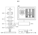
- FIG. 2 shows the principle of the length measurement SEM.
- the primary electron beam emitted from the electron gun 010 is narrowed down by a converging lens 011 and scanned on the sample two-dimensionally by a deflector 012 (scanning coil).
- the control device 015 By irradiating an electron beam focused on the surface of the sample 020 with the objective lens 013, secondary electrons generated from the sample 020 are captured by the detector 014, whereby an electron beam image is obtained. Since more secondary electrons are generated at the pattern edge portion, the electron beam image is a bright image at the portion corresponding to the pattern edge. A series of operations is performed by the control device 015.
- the magnification of the scanned image can be arbitrarily changed by the ratio of the scanning width on the CRT (constant) and the scanning width of the electron beam on the sample (variable).
- the magnification of SEM is M and the pattern dimension on the screen is l
- the actual dimension S is expressed by l / M.
- the length measuring SEM a place where the dimension is measured is designated by the scanning image, and the dimension is measured by calculating from the magnification using the signal waveform of the portion.
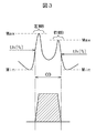
- the “threshold method” which is a representative method, is shown in FIG.
- the portions with large signal amounts corresponding to the left and right pattern edges are referred to as a left white band (left WB) and a right white band (right WB), respectively.
- the threshold method the Max value and the Min value are calculated for each of the left and right WBs, the threshold value is calculated from these values, the position where the signal waveform crosses the threshold value is detected as the edge position, and the distance between the left and right edges is The dimension (CD value) is used. Note that the threshold value in FIG. 3 can be arbitrarily determined by the user.
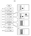
- Fig. 4 shows a general automatic dimension measurement sequence.
- a wafer is carried in (step 101), the stage is moved to the vicinity of the dimension measurement position (step 102), and an image is taken at a low magnification of about 10,000 times (step 103).
- the exact position of the dimension measurement location is obtained by pattern recognition using the registered image as a template (step 104).
- step 105 By limiting the scanning range of the primary electron beam to a narrower range centered on the obtained position (step 105), a high-magnification image of about 150,000 times is captured (step 106), and the dimensions are measured (step 108). .
- image shift The above operation of changing the image capturing position by changing the scanning position of the primary electron beam without moving the stage is called image shift. Without taking a high-magnification image from the beginning, taking a low-magnification image and then taking a high-magnification image by image shift generally includes the measurement target pattern in the high-magnification image due to insufficient stage stop accuracy. Because it is difficult.
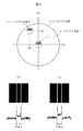
- > 0) is compared with the dimension measurement value (FIG. 5C) obtained from the line pattern image, the position II has a larger beam diameter. The measured value increases. As described above, since the stage stop position varies within a certain accuracy, the image shift amount fluctuates accordingly, which leads to fluctuations in dimension measurement values.
- An object of the present invention is to provide a charged particle beam apparatus having a function of preventing a reduction in measurement reproducibility caused by an increase in beam diameter caused by an image shift and dealing with occurrence of machine differences.
- the present invention scans a primary charged particle beam converged on a sample, detects a secondary charged particle emitted from the sample, and uses a line profile obtained by the pattern on the sample.
- a charged particle beam apparatus for measuring dimensions means for creating and storing a look-up table that correlates an image shift position and a beam diameter change of a primary charged particle beam, means for storing an image shift position when a line profile is acquired, By means of applying the stored image shift position to the lookup table, there is provided means for calculating the beam diameter change at the time of acquiring the line profile, and means for reflecting the calculated beam diameter change in the dimension measurement processing. Is.
- the reduction in measurement reproducibility and the machine difference caused by the change in the beam diameter are improved.
- the present invention is applicable to various types of charged particle beam devices (SEM, FIB (Focused Ion Beam), etc.), but in the following examples, description will be made on SEM as a representative.
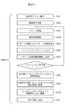
- FIG. 1 shows a flow of dimension measurement in the charged particle beam apparatus according to the present invention.
- Each step of wafer loading (step 101), stage movement (step 102), low-magnification imaging (step 103), pattern recognition (step 104), image shift (step 105), and high-magnification imaging (step 106) is a background art. As described in.
- the image shift position (dx, dy) at the time of taking a high-magnification image is stored (step 301), and the correspondence between the image shift position and the correction coefficient of the image or profile is described according to the stored image shift position.
- the image or profile is corrected with reference to the look-up table (step 302). Then, dimension measurement is performed using the corrected image or profile (step 107).
- FIG. 6 shows a flow for creating the lookup table used in step 302.
- the look-up table describes the correspondence between the image shift position and the image or profile correction coefficient based on the measured value of the image shift vs. beam diameter change measured using a dedicated wafer.
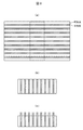
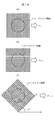
- a wafer having a pattern in which the same cross-sectional shape is continuous as shown in FIG. 7A is suitable.
- images are taken without image shift (image shift position I) and with image shift (image shift position II), and the difference in the gradient of the line profile between these images is quantified.
- the difference in the beam diameter is obtained by the method (described later).
- the above quantified result includes not only the difference in the beam diameter but also the difference in the cross-sectional shape of the pattern. Therefore, it is desirable that the cross-sectional shape of the pattern, particularly the taper angle, be uniform.
- FIG. 8A material A and material B are alternately formed and cut out (FIG. 8 ( b)), a pattern formed by a method in which only the material A is selectively etched (FIG. 8C) and mounted on the wafer is suitable.
- the pattern formed by this method has a small line edge roughness, and the taper angle of the pattern edge is constant (vertical) everywhere.
- a pattern having the same taper angle may be formed by using a single crystal wafer and performing selective etching according to the crystal plane. In the case of a Si wafer, if a wafer having a surface of 110 is used, a pattern having a vertical taper can be formed.
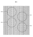
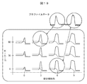
- FIG. 9 shows a case where the pattern is used at four places (410 to 413). Contamination adheres to the location once imaged, so it is necessary to prevent the usage locations from overlapping each other as shown in FIG.
- the dedicated wafer is carried in (step 201), and imaging conditions such as acceleration voltage and beam opening angle are designated (step 202).
- the stage is moved to the image capturing location (step 203), an image is captured at a low magnification (step 204), the arrangement of line patterns is obtained by pattern recognition, and N image shift positions are calculated (step 205).
- N 49 (7 ⁇ 7).
- the image shift is performed based on the calculation result (step 206), and the acquisition of the high-magnification image (step 207) is repeated.
- a feature amount is obtained from the line profile in each image (step 208).
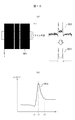
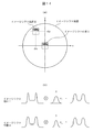
- a line profile 002 is a cross-sectional waveform of the electron beam image 001.
- line addition is performed in the j direction, and a line profile 003 after N line addition in which noise is sufficiently reduced is obtained.
- FIG. 10B is an enlarged view of the left white band (WB) portion of the line profile 003.
- the relationship between the beam diameter and the gradient of the line profile is that the smaller the beam diameter is, the larger the gradient of the line profile is. Therefore, (a) the average gradient between i1 and i2, (b) The maximum gradient between i1 and i2 is considered.
- (c) the WB width (i3-i1) and (d) the outer WB width (i2-i1) may be used. In the case of (c) and (d), on the contrary to (a) and (b), the smaller the beam diameter, the smaller the feature value.
- the feature amount obtained in each image is converted into a correction coefficient used in step 303 in FIG.
- N feature quantities are compared to determine where the beam diameter is maximum within the image shift range. That is, the image shift position that minimizes the feature amount is used when the feature amounts (a) to (b) are used, and the feature amount is displayed when the feature amounts (c) to (d) are used. Find the maximum image shift position.
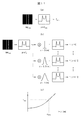
- FIG. 11A A specific method for calculating the correction coefficient is shown in FIG.
- a feature amount calculated from a line profile prof max of an image img max captured at an image shift position where the beam diameter is maximum is assumed to be f max .
- the line profile prof n image img n captured by the respective image shift positions, as in FIG. 11 (b), calculates a characteristic quantity convolution Gaussian function of various ⁇ values. Since the large ⁇ value is the same as the large beam diameter, as the ⁇ value increases, the feature values (a) to (b) become smaller and the feature values (c) to (d) become larger. Become.
- FIG. 11C shows the relationship between the ⁇ value and the feature amount when the feature amounts (c) to (d) are used. Correction factors of image shift positions where the image img n is imaged, sigma ans in FIG 11 (c) (unit nm) the value of. The value of the correction coefficient obtained in this way is 0 (nm) at the position where the beam diameter is maximum, and becomes larger as the position where the beam diameter is smaller.
- the profile prof n is measured at a predetermined image shift position.
- Various correction amounts ⁇ are convolved with the profile prof n to calculate the feature amount f in each case.
- FIG. 11C shows the relationship of changes in the feature amount when the correction amount ⁇ is changed at a predetermined position.
- the correction amount ⁇ ans that has been examined in advance and becomes the same feature amount as the feature amount f max at the position where the beam diameter is maximum is the correction amount at the predetermined position. That is, the graph of FIG. 11C needs to be created for all measurement positions.
- the correction factor is the case where the considered beam intensity distribution with a Gaussian function, img beam diameter of n at a position of the captured bw n and img square root of the square difference of the beam diameter bw max of max at the position of the captured ((bw max 2 -bw n 2 ) 1/2 ). It is a function of only bw max and bw n , and the value does not change even if any of (a) to (d) is used as the feature quantity or depending on the wafer to be used.
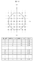
- FIG. 12 shows the structure of the lookup table.
- correction coefficients are registered at each image shift position (crossing position of the broken line in FIG. 12A) within a range of ⁇ 18 microns at intervals of 6 microns vertically and horizontally.
- the tendency of the beam diameter change due to image shift differs depending on the imaging conditions such as acceleration voltage and beam opening angle, so a lookup table is created and registered for each imaging condition.
- the charged particle beam apparatus has a function of displaying a lookup table (step 211 in FIG. 6).
- a desired lookup table is selected from the list of lookup tables registered at that time (FIG. 13A)
- the relationship between the image shift position and the correction coefficient is displayed (FIG. 13B).
- the acceleration voltage is the anode voltage of the electron microscope
- the mode is the electron beam focusing mode. That is, mode H is a high resolution mode, and L is a low resolution mode.
- FIG. 13B shows the relationship between the image shift position and the correction coefficient expressed by contour lines.
- the display of the look-up table can be used not only for checking the contents of the look-up table but also for determining the necessity of readjustment of the optical system. That is, if the correction coefficient exceeds a specified value within a predetermined image shift range, it is determined that the optical system needs to be readjusted.
- the coordinate system of the beam deflection system may be shifted so that they match.
- the lookup table is referred to according to the image shift position (dx, dy) stored in step 301 (step 302). As shown in FIG. 12, since the correction coefficients at the discrete image shift positions are registered in the look-up table, the correction coefficients at (dx, dy) are corrections at the image shift positions at four neighboring positions. Find the coefficients by interpolation.
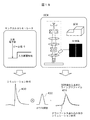
- Fig. 14 shows how to correct the profile.
- the profile correction is realized by convolving a Gaussian function of the ⁇ value registered in the lookup table in accordance with each image shift position.
- the line profile before correction is smaller in II, and the dimension measurement value of II is I. It becomes larger than the dimension measurement value.
- the line profile after convolution is the same, and therefore the dimension measurement values are also equal.
- the convolution of the Gaussian function may be performed on the line profile after once generating the line profile, or the line profile may be generated after convolution of the Gaussian function on the image.
- the present invention since the dimension measurement results are equal regardless of the image shift position, the variation in the dimension measurement value caused by the stage stop position error, which has been a problem in the conventional apparatus, is improved, and the measurement reproducibility is improved. .
- a correction coefficient for correcting a profile or an image is obtained.
- a change amount of a dimension measurement value at each image shift position is checked in advance, and the result is looked up. You may make it register to a table.
- FIG. 15 shows the structure of the lookup table. What is described in the lookup table is an offset value that adjusts the dimension measurement result.
- the lookup table in the first embodiment is registered for each imaging condition, the amount of change in the dimension measurement value varies depending on the measurement target pattern, so the imaging condition (acceleration voltage, beam opening angle, etc.) Each measurement target pattern needs to be registered, but this embodiment is effective when the number of measurement target pattern types is small.
- the relationship between the image shift position and the beam diameter change is obtained by actual measurement in the flow shown in FIG. 6, but the beam diameter at each image shift position is obtained by calculation using an electron optical system simulator.
- the result may be converted into a correction coefficient and registered in the lookup table.
- This calculation result is registered in a lookup table as shown in FIG. 12 as in the first embodiment, and a profile or image is obtained by the method shown in FIG. 14B as in the first embodiment. Perform the correction.
- the relationship between the image shift position and the beam diameter change is obtained using a vertical line pattern, and the ⁇ value of a one-dimensional Gaussian function is used as a correction coefficient.
- ⁇ shown in FIG. 16 A two-dimensional Gaussian function expressed by three parameters of the major axis a of the value, the minor axis b of the ⁇ value, and the angle ⁇ is used.
- a, b, and ⁇ are obtained as follows. (1) The flow shown in FIG. 6 is performed in vertical, horizontal, and diagonal patterns, and correction coefficients ⁇ 0 , ⁇ ⁇ / 2 , and ⁇ ⁇ / 4 are obtained respectively (see FIG. 16). (2) The unknowns a, b, and ⁇ are obtained by solving the simultaneous equations in FIG. Note that ⁇ / 2 in the second equation is the pattern direction of the horizontal pattern, and ⁇ / 4 in the third equation is the pattern direction of the oblique pattern. Although it is difficult to solve these simultaneous equations analytically, a, b, and ⁇ can be uniquely obtained by numerical calculation.
- one correction coefficient is registered for each image shift position (see FIG. 12).
- three correction coefficients a, b, and ⁇ are registered.
- a correction coefficient consisting of is registered.
- the correction process in step 303 in FIG. 1 is performed by (1) convolving a two-dimensional Gaussian function expressed by a, b, ⁇ with respect to the image, or (2) in the direction ⁇ with respect to the line profile. Accordingly, it is realized by convolving a one-dimensional Gaussian function having the ⁇ value calculated in FIG.
- the present embodiment it is possible to cope with a case where the beam diameter change due to the image shift is not isotropic, for example, a case where the change tendency of the beam diameter is different between the horizontal direction and the vertical direction. .
- the vertical line pattern is the measurement target
- the measurement target is a hole pattern measurement or a pattern in which various directions are mixed. It is valid.
- the correction coefficient is obtained by quantifying the change in the gradient of the line profile caused by the change in the beam diameter.
- the correction coefficient is obtained by the method shown in FIG.
- a secondary electron signal waveform 430 at a beam diameter of zero is obtained by Monte Carlo simulation, and from this and a line profile 431 obtained from an actual SEM image, when the Gaussian function 432 is convoluted to 430, 431 is the most. Find the ⁇ value of the Gaussian function that matches.
- This calculation result is registered in a lookup table as shown in FIG. 12 as in the first embodiment, and a profile or image is obtained by the method shown in FIG. 14B as in the first embodiment. Perform the correction.
- FIG. 19 is a diagram in which a corner R and an inclination of a step are estimated based on a beam profile using a library created in advance.
- a library of beam profiles and correction amounts is created for each image shift position, and the correction amount is determined by referring to the library.
- a continuous line pattern as shown in FIG. 7 is used.
- one pattern edge is used to move the stage ⁇ on one pattern edge.
- Image capture at multiple locations (FIG. 20 (a))
- stage movement ⁇ image capture at multiple locations on one pattern edge (FIG. 20 (b)) ⁇ ...
- An image at a position is taken.
- the overall flow is shown in FIG.
- the flow of FIG. 21 is the same as the flow described in FIG. 6 except that the stage is moved every time one pattern edge is measured.
- the obtained data set cannot be a uniform pitch within the image shift range as in the first embodiment, and is indicated by a circle in FIG. Thus, the data becomes non-uniform pitch.
- the data is converted into uniform pitch data as shown in FIG.
- the registered lookup table is used in the same manner as in the first embodiment.
- the difference in the cross-sectional shape of the pattern depending on the location becomes an error factor when obtaining the relationship between the image shift position and the beam diameter.
- This embodiment has the demerit that the time required for creating the lookup table increases because the stage needs to be moved, but has the advantage that the above error factors are reduced.
- the dimensional measurement value differs depending on the image shift position in one device.
- the difference between the devices that is, the dimensional measurement value between the devices is different. Address the differences.
- the sequence 200 shown in FIG. 6 or FIG. 21 is performed in each apparatus to find the maximum value of the beam diameter at all image shift positions of all apparatuses.
- a correction coefficient is set so that the line profile at all image shift positions is equal.
- Electron beam image 002 ... Line profile, 003 ... Line profile after N line addition, 010 ... Electron gun, 011 ... Focusing lens, 012 ... Deflector, 013 ... Objective lens, 014 ... Detector, 015 ... Control device 020 ... Sample.
Landscapes
- Chemical & Material Sciences (AREA)
- Analytical Chemistry (AREA)
- Physics & Mathematics (AREA)
- Electromagnetism (AREA)
- General Physics & Mathematics (AREA)
- Length-Measuring Devices Using Wave Or Particle Radiation (AREA)
Abstract
Description
(1)図6に示すフローを縦,横,斜めの各パターンにて行い,それぞれで補正係数σ0,σπ/2,σπ/4を求める(図16参照)。
(2)図17(b)の連立方程式を解くことで,未知数a,b,θを求める。なお,第2式のπ/2は横パターンのパターン方向であり,第3式のπ/4は斜めパターンのパターン方向である。この連立方程式を解析的に解くのは困難であるが,数値計算を行えばa,b,θは一意に求まる。
Claims (7)
- 試料上に収束した一次荷電粒子線を走査して,試料から放出される二次荷電粒子を検出して得られるラインプロファイルを用いて前記試料上のパターン寸法を計測する荷電粒子線装置であって,
イメージシフト位置と前記一次荷電粒子線のビーム径変化を関連づけるルックアップテーブルを作成し保有する手段と,
前記ラインプロファイル取得時の前記イメージシフト位置を記憶する手段と,
前記記憶されたイメージシフト位置を前記ルックアップテーブルに当てはめることにより前記ラインプロファイル取得時のビーム径変化を算出する手段と,
前記算出されたビーム径変化を寸法計測処理に反映する手段とを有することを特徴とする荷電粒子線装置。 - 試料上に収束した一次荷電粒子線を走査して,試料から放出される二次荷電粒子を検出して得られるラインプロファイルを用いて試料上のパターン寸法を計測する荷電粒子線装置であって,
イメージシフト位置と前記一次荷電粒子線のビーム径変化を関連づけるルックアップテーブルを作成し保有する手段と,
前記ルックアップテーブルを参照して,前記イメージシフト位置と前記一次荷電粒子線のビーム径変化の関係が,規定の条件を満たすか否かの判断する手段を有することを特徴とする荷電粒子線装置。 - 請求項1ないし2に記載の荷電粒子線装置であって,前記ルックアップテーブルが撮像条件とリンクしていることを特徴とする荷電粒子線装置。
- 請求項1ないし2に記載の荷電粒子線装置であって,
前記イメージシフト位置と前記一次荷電粒子線のビーム径変化を関連づけるモデルを作成し保有する手段は,
種々のイメージシフト位置にてステップエッジを有する試料のラインプロファイルを取得し,前記ラインプロファイル上の試料のエッジ部に相当する箇所の波形の急峻さを定量化した特徴量と前記イメージシフト位置を関連づけたものであることを特徴とする荷電粒子線装置。 - 請求項1ないし2に記載の荷電粒子線装置であって,前記ビーム径変化が二次元のガウス関数で表現されることを特徴とする荷電粒子線装置。
- 請求項1に記載の荷電粒子線装置であって,前記ビーム径変化を寸法計測処理に反映する手段は,前記ラインプロファイルに対して,前記ビーム径の変化を補償するガウス関数の畳み込みにより実施されることを特徴とする荷電粒子線装置。
- 複数の荷電粒子線装置からなる測定システムにおいて,
前記荷電粒子線装置は、試料上に収束した一次荷電粒子線を走査して,試料から放出される二次荷電粒子を検出して得られるラインプロファイルを用いて前記試料上のパターン寸法を計測する荷電粒子線装置であって,
イメージシフト位置と前記一次荷電粒子線のビーム径変化を関連づけるルックアップテーブルを作成し保有する手段と,
前記ラインプロファイル取得時の前記イメージシフト位置を記憶する手段と,
前記記憶された前記イメージシフト位置を前記ルックアップテーブルに当てはめることにより前記ラインプロファイル取得時のビーム径変化を算出する手段と,
前記算出されたビーム径変化を寸法計測処理に反映する手段とを有し、
前記ルックアップテーブルは複数の前記荷電粒子線装置の寸法計測値を共通に補正するものであることを特徴とする測定システム。
Priority Applications (2)
| Application Number | Priority Date | Filing Date | Title |
|---|---|---|---|
| KR1020117017575A KR101235963B1 (ko) | 2009-01-28 | 2010-01-26 | 하전 입자선 장치 |
| US13/146,436 US8357897B2 (en) | 2009-01-28 | 2010-01-26 | Charged particle beam device |
Applications Claiming Priority (2)
| Application Number | Priority Date | Filing Date | Title |
|---|---|---|---|
| JP2009-016550 | 2009-01-28 | ||
| JP2009016550A JP4929296B2 (ja) | 2009-01-28 | 2009-01-28 | 荷電粒子線装置 |
Publications (1)
| Publication Number | Publication Date |
|---|---|
| WO2010087149A1 true WO2010087149A1 (ja) | 2010-08-05 |
Family
ID=42395414
Family Applications (1)
| Application Number | Title | Priority Date | Filing Date |
|---|---|---|---|
| PCT/JP2010/000423 Ceased WO2010087149A1 (ja) | 2009-01-28 | 2010-01-26 | 荷電粒子線装置 |
Country Status (4)
| Country | Link |
|---|---|
| US (1) | US8357897B2 (ja) |
| JP (1) | JP4929296B2 (ja) |
| KR (1) | KR101235963B1 (ja) |
| WO (1) | WO2010087149A1 (ja) |
Cited By (1)
| Publication number | Priority date | Publication date | Assignee | Title |
|---|---|---|---|---|
| CN116206935A (zh) * | 2023-05-04 | 2023-06-02 | 华芯程(杭州)科技有限公司 | 一种晶圆测量机台的校准方法、装置及设备 |
Families Citing this family (8)
| Publication number | Priority date | Publication date | Assignee | Title |
|---|---|---|---|---|
| WO2010073360A1 (ja) * | 2008-12-26 | 2010-07-01 | 株式会社アドバンテスト | パターン測定装置及びパターン測定方法 |
| JP5588944B2 (ja) * | 2011-09-05 | 2014-09-10 | 株式会社日立ハイテクノロジーズ | 走査型電子顕微鏡 |
| EP2816585A1 (en) * | 2013-06-17 | 2014-12-24 | ICT Integrated Circuit Testing Gesellschaft für Halbleiterprüftechnik mbH | Charged particle beam system and method of operating thereof |
| JP6865465B2 (ja) * | 2017-11-10 | 2021-04-28 | 株式会社日立ハイテク | パターン計測装置および計測方法 |
| JP7267882B2 (ja) * | 2019-09-17 | 2023-05-02 | キオクシア株式会社 | 基板、パターン、及び計測装置の較正方法 |
| US10943763B1 (en) * | 2019-09-24 | 2021-03-09 | Applied Materials, Inc. | Use of electron beam scanning electron microscopy for characterization of a sidewall occluded from line-of-sight of the electron beam |
| WO2023232257A1 (en) * | 2022-06-02 | 2023-12-07 | Applied Materials, Inc. | Method for calibrating deflectors of a charged particle beam device, and charged particle beam device |
| JP2024008451A (ja) * | 2022-07-08 | 2024-01-19 | 株式会社日立ハイテク | 荷電粒子線装置 |
Citations (10)
| Publication number | Priority date | Publication date | Assignee | Title |
|---|---|---|---|---|
| JPH01293478A (ja) * | 1988-05-23 | 1989-11-27 | Hitachi Ltd | パターン検査方法 |
| JPH06110397A (ja) * | 1992-06-03 | 1994-04-22 | Internatl Business Mach Corp <Ibm> | 電子ビーム投射偏向装置 |
| JPH10106469A (ja) * | 1996-09-30 | 1998-04-24 | Toshiba Corp | 非点収差補正方法及び非点収差補正装置 |
| JP2003121132A (ja) * | 2001-10-12 | 2003-04-23 | Hitachi High-Technologies Corp | 試料の測長方法、及び走査顕微鏡 |
| JP2005156436A (ja) * | 2003-11-27 | 2005-06-16 | Hitachi Ltd | 半導体パターン計測方法、およびプロセス管理方法 |
| JP2005285746A (ja) * | 2004-03-03 | 2005-10-13 | Hitachi High-Technologies Corp | 走査型電子顕微鏡を用いた試料の観察方法及びその装置 |
| JP2005322423A (ja) * | 2004-05-06 | 2005-11-17 | Hitachi High-Technologies Corp | 電子顕微鏡装置およびそのシステム並びに電子顕微鏡装置およびそのシステムを用いた寸法計測方法 |
| JP2006153837A (ja) * | 2004-10-29 | 2006-06-15 | Hitachi High-Technologies Corp | 走査型電子顕微鏡及びそれを用いたパターン計測方法並びに走査型電子顕微鏡の機差補正装置 |
| JP2007194007A (ja) * | 2006-01-18 | 2007-08-02 | Hitachi High-Technologies Corp | 走査型電子顕微鏡、その保守・管理プログラム、保守・管理方法および走査型電子顕微鏡システムにおける資源割り当て方法 |
| JP2009016181A (ja) * | 2007-07-04 | 2009-01-22 | Fujitsu Ltd | 試料観察装置とその補正方法 |
Family Cites Families (1)
| Publication number | Priority date | Publication date | Assignee | Title |
|---|---|---|---|---|
| JP4791141B2 (ja) * | 2005-10-25 | 2011-10-12 | 株式会社日立ハイテクノロジーズ | 電子線式寸法計測装置及びそれを用いた寸法計測方法 |
-
2009
- 2009-01-28 JP JP2009016550A patent/JP4929296B2/ja active Active
-
2010
- 2010-01-26 US US13/146,436 patent/US8357897B2/en active Active
- 2010-01-26 KR KR1020117017575A patent/KR101235963B1/ko active Active
- 2010-01-26 WO PCT/JP2010/000423 patent/WO2010087149A1/ja not_active Ceased
Patent Citations (10)
| Publication number | Priority date | Publication date | Assignee | Title |
|---|---|---|---|---|
| JPH01293478A (ja) * | 1988-05-23 | 1989-11-27 | Hitachi Ltd | パターン検査方法 |
| JPH06110397A (ja) * | 1992-06-03 | 1994-04-22 | Internatl Business Mach Corp <Ibm> | 電子ビーム投射偏向装置 |
| JPH10106469A (ja) * | 1996-09-30 | 1998-04-24 | Toshiba Corp | 非点収差補正方法及び非点収差補正装置 |
| JP2003121132A (ja) * | 2001-10-12 | 2003-04-23 | Hitachi High-Technologies Corp | 試料の測長方法、及び走査顕微鏡 |
| JP2005156436A (ja) * | 2003-11-27 | 2005-06-16 | Hitachi Ltd | 半導体パターン計測方法、およびプロセス管理方法 |
| JP2005285746A (ja) * | 2004-03-03 | 2005-10-13 | Hitachi High-Technologies Corp | 走査型電子顕微鏡を用いた試料の観察方法及びその装置 |
| JP2005322423A (ja) * | 2004-05-06 | 2005-11-17 | Hitachi High-Technologies Corp | 電子顕微鏡装置およびそのシステム並びに電子顕微鏡装置およびそのシステムを用いた寸法計測方法 |
| JP2006153837A (ja) * | 2004-10-29 | 2006-06-15 | Hitachi High-Technologies Corp | 走査型電子顕微鏡及びそれを用いたパターン計測方法並びに走査型電子顕微鏡の機差補正装置 |
| JP2007194007A (ja) * | 2006-01-18 | 2007-08-02 | Hitachi High-Technologies Corp | 走査型電子顕微鏡、その保守・管理プログラム、保守・管理方法および走査型電子顕微鏡システムにおける資源割り当て方法 |
| JP2009016181A (ja) * | 2007-07-04 | 2009-01-22 | Fujitsu Ltd | 試料観察装置とその補正方法 |
Cited By (1)
| Publication number | Priority date | Publication date | Assignee | Title |
|---|---|---|---|---|
| CN116206935A (zh) * | 2023-05-04 | 2023-06-02 | 华芯程(杭州)科技有限公司 | 一种晶圆测量机台的校准方法、装置及设备 |
Also Published As
| Publication number | Publication date |
|---|---|
| US8357897B2 (en) | 2013-01-22 |
| JP4929296B2 (ja) | 2012-05-09 |
| KR20110110243A (ko) | 2011-10-06 |
| JP2010175318A (ja) | 2010-08-12 |
| KR101235963B1 (ko) | 2013-02-21 |
| US20120104254A1 (en) | 2012-05-03 |
Similar Documents
| Publication | Publication Date | Title |
|---|---|---|
| JP4929296B2 (ja) | 荷電粒子線装置 | |
| JP5156619B2 (ja) | 試料寸法検査・測定方法、及び試料寸法検査・測定装置 | |
| US7750296B2 (en) | Scanning electron microscope and calibration of image distortion | |
| US8330104B2 (en) | Pattern measurement apparatus and pattern measurement method | |
| US8214166B2 (en) | Method and its system for calibrating measured data between different measuring tools | |
| US8878925B2 (en) | Observation method and observation device | |
| JP2007218711A (ja) | 電子顕微鏡装置を用いた計測対象パターンの計測方法 | |
| US20080015813A1 (en) | Pattern measurement apparatus and pattern measuring method | |
| JP4500099B2 (ja) | 電子顕微鏡装置システム及び電子顕微鏡装置システムを用いた寸法計測方法 | |
| US20090212215A1 (en) | Scanning electron microscope and method of measuring pattern dimension using the same | |
| TW202029268A (zh) | 電子束觀察裝置,電子束觀察系統,電子束觀察裝置中的圖像修正方法及用於圖像修正的修正係數算出方法 | |
| TWI698705B (zh) | 圖案測定方法、及圖案測定裝置 | |
| JP2007187538A (ja) | 荷電粒子線装置及びそれを用いた画像取得方法 | |
| KR102154667B1 (ko) | 패턴 계측 장치, 및 컴퓨터 프로그램 | |
| JP5321775B2 (ja) | パターン検査方法およびパターン検査装置 | |
| KR102821519B1 (ko) | 하전 입자선 장치 및 검사 장치 | |
| JP2011179819A (ja) | パターン測定方法及びコンピュータプログラム | |
| US9200896B2 (en) | Pattern dimension measurement method and charged particle beam microscope used in same | |
| JP4922710B2 (ja) | 電子顕微鏡の分解能評価用試料及び電子顕微鏡の分解能評価方法並びに電子顕微鏡 | |
| JP2016217816A (ja) | パターン計測装置、パターン計測方法およびパターン計測プログラム | |
| CN115380207B (zh) | 图案匹配方法 | |
| JP2010160080A (ja) | 荷電粒子線を用いた寸法計測方法、および寸法計測装置 | |
| JP2006073286A (ja) | パターン検査装置 | |
| WO2025062546A1 (ja) | 検査計測モデルを有する走査型電子顕微鏡及び検査計測モデルの修正方法 | |
| WO2022249489A1 (ja) | 深さ計測装置、深さ計測システム及び深さ指標値算出方法 |
Legal Events
| Date | Code | Title | Description |
|---|---|---|---|
| 121 | Ep: the epo has been informed by wipo that ep was designated in this application |
Ref document number: 10735621 Country of ref document: EP Kind code of ref document: A1 |
|
| ENP | Entry into the national phase |
Ref document number: 20117017575 Country of ref document: KR Kind code of ref document: A |
|
| NENP | Non-entry into the national phase |
Ref country code: DE |
|
| WWE | Wipo information: entry into national phase |
Ref document number: 13146436 Country of ref document: US |
|
| 122 | Ep: pct application non-entry in european phase |
Ref document number: 10735621 Country of ref document: EP Kind code of ref document: A1 |