WO2010087139A1 - 型および型の製造方法ならびに型を用いた反射防止膜の製造方法 - Google Patents
型および型の製造方法ならびに型を用いた反射防止膜の製造方法 Download PDFInfo
- Publication number
- WO2010087139A1 WO2010087139A1 PCT/JP2010/000358 JP2010000358W WO2010087139A1 WO 2010087139 A1 WO2010087139 A1 WO 2010087139A1 JP 2010000358 W JP2010000358 W JP 2010000358W WO 2010087139 A1 WO2010087139 A1 WO 2010087139A1
- Authority
- WO
- WIPO (PCT)
- Prior art keywords
- mold
- conductive layer
- film
- porous alumina
- alumina layer
- Prior art date
- Legal status (The legal status is an assumption and is not a legal conclusion. Google has not performed a legal analysis and makes no representation as to the accuracy of the status listed.)
- Ceased
Links
Images





Classifications
-
- G—PHYSICS
- G02—OPTICS
- G02B—OPTICAL ELEMENTS, SYSTEMS OR APPARATUS
- G02B1/00—Optical elements characterised by the material of which they are made; Optical coatings for optical elements
- G02B1/10—Optical coatings produced by application to, or surface treatment of, optical elements
- G02B1/11—Anti-reflection coatings
- G02B1/118—Anti-reflection coatings having sub-optical wavelength surface structures designed to provide an enhanced transmittance, e.g. moth-eye structures
-
- B—PERFORMING OPERATIONS; TRANSPORTING
- B29—WORKING OF PLASTICS; WORKING OF SUBSTANCES IN A PLASTIC STATE IN GENERAL
- B29C—SHAPING OR JOINING OF PLASTICS; SHAPING OF MATERIAL IN A PLASTIC STATE, NOT OTHERWISE PROVIDED FOR; AFTER-TREATMENT OF THE SHAPED PRODUCTS, e.g. REPAIRING
- B29C33/00—Moulds or cores; Details thereof or accessories therefor
- B29C33/38—Moulds or cores; Details thereof or accessories therefor characterised by the material or the manufacturing process
- B29C33/3828—Moulds made of at least two different materials having different thermal conductivities
-
- B—PERFORMING OPERATIONS; TRANSPORTING
- B29—WORKING OF PLASTICS; WORKING OF SUBSTANCES IN A PLASTIC STATE IN GENERAL
- B29C—SHAPING OR JOINING OF PLASTICS; SHAPING OF MATERIAL IN A PLASTIC STATE, NOT OTHERWISE PROVIDED FOR; AFTER-TREATMENT OF THE SHAPED PRODUCTS, e.g. REPAIRING
- B29C33/00—Moulds or cores; Details thereof or accessories therefor
- B29C33/42—Moulds or cores; Details thereof or accessories therefor characterised by the shape of the moulding surface, e.g. ribs or grooves
- B29C33/424—Moulding surfaces provided with means for marking or patterning
-
- B—PERFORMING OPERATIONS; TRANSPORTING
- B29—WORKING OF PLASTICS; WORKING OF SUBSTANCES IN A PLASTIC STATE IN GENERAL
- B29C—SHAPING OR JOINING OF PLASTICS; SHAPING OF MATERIAL IN A PLASTIC STATE, NOT OTHERWISE PROVIDED FOR; AFTER-TREATMENT OF THE SHAPED PRODUCTS, e.g. REPAIRING
- B29C33/00—Moulds or cores; Details thereof or accessories therefor
- B29C33/56—Coatings, e.g. enameled or galvanised; Releasing, lubricating or separating agents
- B29C33/60—Releasing, lubricating or separating agents
- B29C33/62—Releasing, lubricating or separating agents based on polymers or oligomers
-
- B—PERFORMING OPERATIONS; TRANSPORTING
- B29—WORKING OF PLASTICS; WORKING OF SUBSTANCES IN A PLASTIC STATE IN GENERAL
- B29C—SHAPING OR JOINING OF PLASTICS; SHAPING OF MATERIAL IN A PLASTIC STATE, NOT OTHERWISE PROVIDED FOR; AFTER-TREATMENT OF THE SHAPED PRODUCTS, e.g. REPAIRING
- B29C35/00—Heating, cooling or curing, e.g. crosslinking or vulcanising; Apparatus therefor
- B29C35/02—Heating or curing, e.g. crosslinking or vulcanizing during moulding, e.g. in a mould
- B29C35/08—Heating or curing, e.g. crosslinking or vulcanizing during moulding, e.g. in a mould by wave energy or particle radiation
- B29C35/0805—Heating or curing, e.g. crosslinking or vulcanizing during moulding, e.g. in a mould by wave energy or particle radiation using electromagnetic radiation
-
- C—CHEMISTRY; METALLURGY
- C25—ELECTROLYTIC OR ELECTROPHORETIC PROCESSES; APPARATUS THEREFOR
- C25D—PROCESSES FOR THE ELECTROLYTIC OR ELECTROPHORETIC PRODUCTION OF COATINGS; ELECTROFORMING; APPARATUS THEREFOR
- C25D11/00—Electrolytic coating by surface reaction, i.e. forming conversion layers
- C25D11/02—Anodisation
- C25D11/04—Anodisation of aluminium or alloys based thereon
- C25D11/045—Anodisation of aluminium or alloys based thereon for forming AAO templates
-
- C—CHEMISTRY; METALLURGY
- C25—ELECTROLYTIC OR ELECTROPHORETIC PROCESSES; APPARATUS THEREFOR
- C25D—PROCESSES FOR THE ELECTROLYTIC OR ELECTROPHORETIC PRODUCTION OF COATINGS; ELECTROFORMING; APPARATUS THEREFOR
- C25D11/00—Electrolytic coating by surface reaction, i.e. forming conversion layers
- C25D11/02—Anodisation
- C25D11/04—Anodisation of aluminium or alloys based thereon
- C25D11/06—Anodisation of aluminium or alloys based thereon characterised by the electrolytes used
-
- C—CHEMISTRY; METALLURGY
- C25—ELECTROLYTIC OR ELECTROPHORETIC PROCESSES; APPARATUS THEREFOR
- C25D—PROCESSES FOR THE ELECTROLYTIC OR ELECTROPHORETIC PRODUCTION OF COATINGS; ELECTROFORMING; APPARATUS THEREFOR
- C25D11/00—Electrolytic coating by surface reaction, i.e. forming conversion layers
- C25D11/02—Anodisation
- C25D11/04—Anodisation of aluminium or alloys based thereon
- C25D11/12—Anodising more than once, e.g. in different baths
-
- C—CHEMISTRY; METALLURGY
- C25—ELECTROLYTIC OR ELECTROPHORETIC PROCESSES; APPARATUS THEREFOR
- C25D—PROCESSES FOR THE ELECTROLYTIC OR ELECTROPHORETIC PRODUCTION OF COATINGS; ELECTROFORMING; APPARATUS THEREFOR
- C25D11/00—Electrolytic coating by surface reaction, i.e. forming conversion layers
- C25D11/02—Anodisation
- C25D11/04—Anodisation of aluminium or alloys based thereon
- C25D11/18—After-treatment, e.g. pore-sealing
- C25D11/24—Chemical after-treatment
Definitions
- the present invention relates to a mold, a method for manufacturing the mold, and a method for manufacturing an antireflection film using the mold.
- the “mold” here includes molds used in various processing methods (stamping and casting), and is sometimes referred to as a stamper. It can also be used for printing (including nanoprinting).
- An optical element such as a display device or a camera lens used for a television or a mobile phone is usually provided with an antireflection technique in order to reduce surface reflection and increase light transmission.
- an antireflection technique in order to reduce surface reflection and increase light transmission. For example, when light passes through the interface of a medium with a different refractive index, such as when light enters the interface between air and glass, the amount of transmitted light is reduced due to Fresnel reflection, and visibility is reduced. is there.
- This method utilizes the principle of a so-called moth-eye structure, and the refractive index for light incident on the substrate is determined from the refractive index of the incident medium along the depth direction of the irregularities, to the refractive index of the substrate.
- the reflection in the wavelength region that is desired to be prevented from being reflected is suppressed by continuously changing the wavelength.
- the moth-eye structure has an advantage that it can exhibit an antireflection effect with a small incident angle dependency over a wide wavelength range, can be applied to many materials, and can form an uneven pattern directly on a substrate. As a result, a low-cost and high-performance antireflection film (or antireflection surface) can be provided.
- Patent Documents 2 to 4 As a method for producing a moth-eye structure, a method using an anodized porous alumina layer obtained by anodizing aluminum is attracting attention (Patent Documents 2 to 4).
- anodized porous alumina layer obtained by anodizing aluminum will be briefly described.
- a method for producing a porous structure using anodization has attracted attention as a simple method capable of forming regularly ordered nano-sized cylindrical pores (fine concave portions).
- an acidic or alkaline electrolyte such as sulfuric acid, oxalic acid, or phosphoric acid
- a voltage is applied using the aluminum substrate as an anode
- oxidation and dissolution proceed simultaneously on the surface of the aluminum substrate.
- An oxide film having pores can be formed. These cylindrical pores are oriented perpendicular to the oxide film and exhibit self-organized regularity under certain conditions (voltage, type of electrolyte, temperature, etc.). Is expected.
- the porous alumina layer produced under specific conditions takes an array in which almost regular hexagonal cells are two-dimensionally filled with the highest density when viewed from the direction perpendicular to the film surface.
- Each cell has a pore in the center, and the arrangement of the pores has periodicity.
- the cell is formed as a result of local dissolution and growth of the film, and dissolution and growth of the film proceed simultaneously at the bottom of the pores called a barrier layer.
- the cell size that is, the distance between adjacent pores (center-to-center distance) corresponds to approximately twice the thickness of the barrier layer and is approximately proportional to the voltage during anodization.
- the diameter of the pores depends on the type, concentration, temperature, etc.
- the pores of such porous alumina have an arrangement with high regularity (having periodicity) under a specific condition, an arrangement with irregularity to some extent or an irregularity (having no periodicity) depending on the conditions. ).
- Patent Document 2 discloses a method of forming an antireflection film (antireflection surface) using a stamper having an anodized porous alumina film on the surface.
- Patent Document 3 discloses a technique for forming a tapered concave portion in which the pore diameter continuously changes by repeating anodization of aluminum and pore diameter enlargement processing.
- Patent Document 4 a technique for forming an antireflection film using an alumina layer in which fine concave portions have stepped side surfaces.
- an antireflection film (antireflection surface) is provided by providing a concavo-convex structure (macro structure) larger than the moth eye structure in addition to the moth eye structure (micro structure). ) Can be given an anti-glare (anti-glare) function.
- the two-dimensional size of the projections that form the projections and depressions that exhibit the antiglare function is 1 ⁇ m or more and less than 100 ⁇ m.
- a mold for forming a moth-eye structure on the surface (hereinafter referred to as “moth-eye mold”) can be easily manufactured.
- the surface of an anodized aluminum film is used as it is as a mold, the effect of reducing the manufacturing cost is great.
- the surface structure of the moth-eye mold that can form the moth-eye structure is referred to as an “inverted moth-eye structure”.
- Non-Patent Document 1 discloses a method for producing a nanoprint mold having optical transparency. After forming an anodized porous alumina film having a desired structure on one surface of the aluminum plate, all the remaining aluminum is anodized from the back surface of the aluminum plate to obtain a light-transmitting mold. A regular pattern of an ultraviolet curable resin formed on a silicon substrate using a mold having optical transparency is disclosed. Thus, the use of a light-transmitting mold provides the advantage that light can be irradiated to the ultraviolet curable resin through the mold.
- Non-Patent Document 1 has the entire mold formed of an anodized porous alumina film and has pores formed on both sides. Therefore, there is a problem that the mold is easily broken. If the mold is made thicker in order to obtain sufficient mechanical strength, there is a problem that it is difficult to anodize the entire aluminum plate.
- Non-Patent Document 1 In the method described in Non-Patent Document 1, an electrode is connected to the end of an aluminum plate to be a mold. Therefore, when a large-area mold is manufactured, it is difficult to anodize the entire aluminum plate. There is a problem. Since aluminum does not have optical transparency, the desired optical transparency mold cannot be obtained.
- Non-Patent Document 1 since the method described in Non-Patent Document 1 includes the step of anodizing the aluminum plate from both sides, it cannot be applied to the aluminum film formed on the substrate.
- the present invention has been made to solve the above-mentioned problems, and its main object is to provide a method for manufacturing a large-area moth-eye mold capable of transmitting ultraviolet rays, and so on.
- An object of the present invention is to provide a moth-eye mold manufactured by a simple manufacturing method.
- the mold of the present invention is a base material, a conductive layer formed on the base material, and an anodized film formed on the conductive layer, which is two-dimensional when viewed from the normal direction of the surface. And an anodic oxide film having an inverted moth-eye structure on the surface, the substrate, the conductive layer, and the anodic oxide film transmitting ultraviolet light. be able to.
- the conductive layer is formed of a titanium film having a thickness of 100 nm or less.
- the thickness of the titanium film is preferably 1 nm or more.
- the mold further includes a release layer formed on the anodized film.
- the release layer is, for example, a water repellent resin layer.
- the anodic oxide film has fine holes smaller than the plurality of recesses on the conductive layer side of the plurality of recesses.
- the anodic oxide film includes a porous alumina layer having the inverted moth-eye structure on its surface, and an alumina layer (“barrier”) formed on the conductive layer side of the porous alumina layer. Layer ”)).
- the thickness of the alumina layer having no micropores is 100 nm or more.
- the thickness of the alumina layer having no micropores is preferably 400 nm or less.
- the mold manufacturing method of the present invention is a mold manufacturing method having an inverted moth-eye structure on the surface having a plurality of recesses having a two-dimensional size of 10 nm or more and less than 500 nm when viewed from the normal direction of the surface.
- A preparing a substrate capable of transmitting ultraviolet light, (b) forming a conductive layer capable of transmitting ultraviolet light on the substrate, and (c) conducting the conductive material.
- a step of forming a layer (d2) After the step (d1), the porous alumina layer is brought into contact with an etchant to thereby form the plurality of fine recesses of the porous alumina layer. Comprising the step of expanding, after the (d3) said step (d2), by further anodization, and growing a plurality of minute recesses to.
- step (d) in the step (d), the step (d2) and the step (d3) are further performed after the step (d3).
- the step (d) includes the step (da) of forming the inverted moth-eye structure on the surface of the porous alumina layer by the steps (d1) to (d3), and the step (da). Thereafter, the method further includes a step (db1) of forming micropores smaller than the plurality of recesses on the conductive layer side of the porous alumina layer by further anodizing.
- the manufacturing method includes a step (db2) of forming an alumina layer having no micropores on the conductive layer side of the porous alumina layer by anodizing after the step (db1). Is further included.
- the step (db2) is performed in an electrolytic solution having a pH higher than 4.0 and lower than 7.0.
- the electrolytic solution used in the step (db2) is tartaric acid, ammonium tartrate, potassium sodium tartrate, boric acid, ammonium borate, ammonium oxalate, ammonium citrate, maleic acid, malonic acid, phthalic acid and An aqueous solution comprising at least one acid or salt selected from the group consisting of citric acid.
- the step (db2) is performed in an acidic aqueous solution having a concentration of 0.1 mol / L or less.
- a low concentration acidic aqueous solution having a sufficiently low dissolving power of aluminum oxide can be used.
- an aqueous phosphoric acid solution having a concentration of 0.1 mol / L or less can be used.
- the method for producing an antireflection film according to the present invention includes a step of preparing any one of the above molds and a workpiece, and a state in which an ultraviolet curable resin is applied between the mold and the surface of the workpiece. And curing the ultraviolet curable resin by irradiating the ultraviolet curable resin with ultraviolet rays through the mold.
- a method for producing a large-area moth-eye mold that can transmit ultraviolet rays in addition, according to the present invention, a novel moth-eye mold that can transmit ultraviolet rays can be provided. Furthermore, according to the present invention, a method for producing an antireflection film using the above mold is provided.
- the present invention is advantageous in that a large-area moth-eye mold can be manufactured, but it goes without saying that the present invention can also be applied to manufacture a small-area moth-eye mold.
- (A) And (b) is a schematic diagram for demonstrating the problem of the conventional anodic oxidation process.
- (A) And (b) is the figure which shows the cross-sectional schematic diagram and SEM image of the type
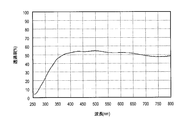
- (a) is the part 90A in which the aluminum film was completely anodized
- (B) shows the cross-sectional structure of the portion 90B where a part of the aluminum film remains. It is a figure which shows the transmission spectrum of 90 A of moth-eye type
- (A)-(c) is a schematic diagram for demonstrating the manufacturing method of the moth-eye type
- (A)-(c) is a figure which shows the SEM image of the cross section of a moth-eye type
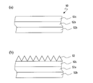
- (A) is a schematic diagram which shows the cross-sectional structure of a polarizing plate
- (b) is a schematic diagram which shows the cross-sectional structure of the polarizing plate in which the antireflection film was formed by the manufacturing method of the antireflection film of embodiment by this invention. is there.
- Two types of glass substrates 10b of 5 cm square and 10 cm square were prepared as base materials capable of transmitting ultraviolet rays.
- An aluminum film 10a having a thickness of 1.0 ⁇ m was deposited on the glass substrate 10b by sputtering. This is designated as Sample 10.
- the anodizing step was performed by immersing the sample 10 of 5 cm square and 10 cm square in the electrolytic solution 26 in the container 24 as shown in FIGS. 1 (a) and 1 (b), respectively.
- the 5 cm square sample 10 was erected with a plastic jig such that the diagonal direction was the vertical direction.
- the 10 cm square sample 10 was set up with a plastic jig so that the pair of sides were in the vertical direction.
- the electrode 22a in contact with the aluminum film 10a was connected to the anode of the external DC power source 22D with a lead wire.
- a tantalum plate 20 that has been subjected to platinum plating of the same size as each sample 10 is used as the cathode in the anodic oxidation process, and an electrode 22c that is in contact with the tantalum plate 20 is connected to the external DC power supply 22D with a lead wire. Connected to the cathode.
- the electrolytic solution 26 an aqueous solution of 0.6% by mass of oxalic acid having a liquid temperature of 5 ° C. was used, and anodization was performed at an applied voltage of 90 V for 25 seconds. Thereafter, the porous alumina layer obtained by anodic oxidation was etched by immersing in a 10% by mass aqueous solution of phosphoric acid having a liquid temperature of 30 ° C.
- the anodic oxidation step and the etching step were alternately performed 5 times (5 times of anodic oxidation and 4 times of etching). The results are as follows.
- the aluminum film 10a can be completely anodized in the vicinity of the electrode 22a, but the anodized aluminum (alumina) does not have conductivity, so that a portion separated from the electrode 22a by about 7 cm or more is an external DC.
- the electrical connection with the power source 22D is cut off, the anodic oxidation does not proceed, and the aluminum film remains.
- the sample which performed only the anodic oxidation process was produced separately, the same result was obtained.
- FIG. 2A the cross-sectional structure of a portion (transparent portion) 90A where the aluminum film 10a is completely anodized is shown in FIG. 2A, and a portion where the aluminum film 10a remains (
- the cross-sectional structure of the opaque portion 90B is shown in FIG.
- Each shows a schematic cross-sectional view and a cross-sectional SEM image.
- the aluminum film 10a is completely anodized, and the porous alumina layer 12a having a plurality of fine recesses 12p is in contact with the glass substrate 10b.
- the fine recess 12p of the mold has a two-dimensional size of 10 nm or more and less than 500 nm when viewed from the normal direction of the surface.
- the distance between the recesses adjacent to each other is preferably 30 nm or more and less than 600 nm (Patent Documents 1, 2, and 4).
- the recess 12p of the porous alumina layer 12a formed here has, for example, an opening diameter of 100 nm to 200 nm, a depth of 900 nm to 1 ⁇ m, and a distance between adjacent recesses 12p of 150 nm to 250 nm.
- a moth-eye mold having a large area is shown in FIG. 4A in order to form an anodized porous alumina layer, that is, to completely anodize an aluminum film.
- the conductive layer 11 is provided on the glass substrate 10b.
- the conductive layer 11 is made of a material that can transmit at least 10% of ultraviolet rays (365 nm) for curing the ultraviolet curable resin.
- the transmittance of the finally obtained mold is preferably 10% or more, and more preferably 40% or more.
- a titanium film having a thickness of 20 nm was used as the conductive layer 11.
- the titanium film was formed by sputtering.
- the thickness of the titanium film may be 1 nm or more and 100 nm or less. If the thickness of the titanium film is less than 1 nm, the conductivity may not be ensured uniformly. If the thickness exceeds 100 nm, the transmittance may be less than 10%.
- titanium is preferable as a material for forming the conductive layer 11.
- An ITO film or an IZO film known as a transparent conductive film can also be used, but these are not preferable from the viewpoint of etching resistance.
- the molybdenum film and the tungsten film are more excellent in etching resistance than the ITO film and the IZO film, but titanium is most preferable because pits may be formed on the surface by the etching.
- anodization and etching were repeated alternately. Specifically, anodization was performed for 25 seconds at an applied voltage of 80 V using a 0.6 mass% aqueous solution of oxalic acid at a liquid temperature of 5 ° C. Then, it etched by immersing in 10 mass% phosphoric acid aqueous solution with a liquid temperature of 30 degreeC for 25 minutes. By this etching, fine concave portions of the porous alumina layer formed in the previous anodic oxidation process are enlarged.
- anodization was performed using an aqueous solution of 0.6% by mass of oxalic acid at a liquid temperature of 5 ° C. with an applied voltage of 80V until the entire mold became transparent.
- a mold 100A schematically showing a cross-sectional structure in (b) was obtained. That is, as shown in FIG. 4B, after forming an inverted moth-eye structure on the surface, anodization is further performed, so that a plurality of recesses 12p (2) are formed on the conductive layer 11 side of the porous alumina layer 12a.
- a fine hole 12s having a dimensional size of 10 nm or more and less than 500 nm and a distance between adjacent recesses of 30 nm or more and less than 600 nm is formed.
- a mold 100A shown in FIG. 4B includes a glass substrate 10b, a conductive layer (titanium film) 11 formed on the glass substrate 10b, and an anodic oxide film (porous alumina layer) 12a formed on the conductive layer 11.
- the aluminum film does not remain between the conductive layer 11 and the porous alumina layer 12a.
- the porous alumina layer 12a shown in FIG. 4B has linear fine holes 12s smaller than the recesses 12p for forming the moth-eye structure on the conductive layer 11 side.
- the cross-sectional structure of the layer 12a has a structure in which a plurality of pencils (tips are cut off) are arranged.
- the shape of the fine holes 12s may be transferred.
- the release layer 14 using, for example, a water repellent resin (for example, a fluororesin).
- a fluororesin for example, an amorphous fluororesin (AF grade: AF1600) manufactured by Mitsui DuPont Fluorochemical Co., Ltd. can be suitably used.
- the release layer 14 can be formed by spin coating a fluororesin, for example.
- the fine holes 12s of the porous alumina layer 12a of the mold 100A can be filled by the following method.
- the micropores 12s are filled by anodizing in a neutral (pH of more than 3.0 and less than 8.0) electrolytic solution. be able to. Therefore, by anodizing in the above electrolytic solution, as a result, as shown in FIG. 4C, an alumina layer (barrier layer) having no fine holes 12s on the conductive layer 11 side of the porous alumina layer 12a. ) 12b can be formed.
- pH of neutral electrolyte solution is more than 4.0 and 7.0 or less.
- the electrolyte is an acid or salt selected from the group consisting of tartaric acid, ammonium tartrate, potassium sodium tartrate, boric acid, ammonium borate, ammonium oxalate, ammonium citrate, maleic acid, malonic acid, phthalic acid and citric acid. It is preferable that it is the aqueous solution containing at least 1 of these.
- the electrolyte solution can replace with the said electrolyte solution and can also use the acidic aqueous solution of the density
- an aqueous phosphoric acid solution having a concentration of 0.1 mol / L or less can be used.
- FIG. 5 shows a state in which the fine pores 12s are filled by anodizing using ammonium tartrate (concentration 0.1 mol / L, pH 6.5, liquid temperature 23.2 ° C.) as a neutral electrolyte.
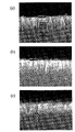
- FIGS. 5 (a) to 5 (c) are SEM images of cross sections of a moth-eye mold showing that the barrier layer 12b (FIG. 4 (c)) is formed by anodic oxidation in a neutral solution. is there.
- the anodic oxidation (the anodic oxidation for forming the moth-eye structure is further performed until the entire mold becomes transparent.
- the anodic oxide film (having the fine holes 12s shown in FIG. 4B) obtained by performing the same conditions as in the step) is anodized for 180 seconds at an applied voltage of 100 V using the above neutral electrolyte. By doing so, as shown to Fig.5 (a), a part of micropore was filled and the barrier layer with a thickness of 96.5 nm was formed. Furthermore, the anodic oxide film shown in FIG.
- 5A is anodized for 180 seconds at an applied voltage of 100 V using the above-described neutral electrolytic solution, and as shown in FIG. As a result, the thickness of the barrier layer was 140 nm. Subsequently, anodization was performed for 180 seconds at an applied voltage of 200 V, so that the thickness of the barrier layer was 253 nm as shown in FIG.
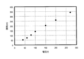
- the thickness of the barrier layer obtained by anodic oxidation using a neutral electrolytic solution depends on the applied voltage, and the results shown in FIG. 6 were obtained for the neutral electrolytic solution.
- the depth of the recess 12p of the porous alumina layer 12a constituting the moth-eye structure is preferably in the range of 150 nm to 500 nm.
- the thickness of the barrier layer 12b is preferably in the range of more than 0 nm and not more than 400 nm.
- the initial thickness of the aluminum film 10a is preferably about 500 nm.
- the initial thickness of the aluminum film 10a is preferably 900 ⁇ m or less from the viewpoint of keeping the thickness of the barrier layer 12b within the above conditions.
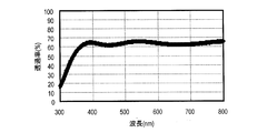
- FIG. 7 shows the transmission spectrum of the mold 100B. As is apparent from FIG. 7, it has a transmittance of about 60% over the entire wavelength range of visible light from ultraviolet rays around 365 nm. A similar transmission spectrum was obtained for the mold 100A. As can be seen by comparing the transmission spectrum of FIG. 7 with the transmission spectrum of FIG. 3, the transmittance of the mold 100B is higher than the transmittance of the moth-eye mold portion 90A (FIG. 2A).
- the reason for this has not yet been confirmed, but compared to the configuration in which the moth-eye structure is directly formed on the glass substrate (type 90A), the alumina substrate (barrier layer) without micropores is formed on the glass substrate, It is considered that the configuration in which the moth-eye structure is formed has less scattering and / or less reflection at the interface.
- a mold 100A or 100B is prepared.
- Ultraviolet curing is performed by irradiating the ultraviolet curable resin 32 with ultraviolet rays (UV) through the mold 100A or 100B with the ultraviolet curable resin 32 applied between the surface of the workpiece 42 and the mold 100A or 100B.
- the resin 32 is cured.
- the ultraviolet curable resin 32 may be applied to the surface of the workpiece 42 or may be applied to the mold surface (surface having a moth-eye structure) of the mold 100A or 100B.
- an acrylic resin can be used as the ultraviolet curable resin 32.
- an antireflection film can be easily formed on the surface of a conventional polarizing plate.
- the polarizing plate 50 shown in FIG. 10A has a polarizing layer 52a formed of PVA and protective layers 52b and 52c sandwiching the polarizing layer 52a.
- the protective layers 52c and 52b are made of, for example, COP (cycloolefin polymer) or TAC.
- COP cycloolefin polymer
- TAC TAC
- ultraviolet irradiation for forming an antireflection film on the polarizing plate 50 cannot be performed from the polarizing plate 50 side.
- ultraviolet rays can be irradiated through the mold, so that an antireflection film 62 having a moth-eye structure is formed on the polarizing plate 50 as shown in FIG. Can be formed.
- the present invention can be widely used for forming an antireflection film.
- the antireflection film can be used for any application where antireflection is desired, including optical elements such as display devices.
- Sample 10b Base material (glass substrate) 10a Aluminum film 10a 'Residual aluminum film 11 Conductive layer 12a Anodized film (porous alumina layer) 12b Barrier layer 12p Concavity (inverted moth-eye structure) 12s Micropore 14 Release layer 100A, 100B Mosaic mold
Landscapes
- Chemical & Material Sciences (AREA)
- Engineering & Computer Science (AREA)
- Materials Engineering (AREA)
- Organic Chemistry (AREA)
- Metallurgy (AREA)
- Chemical Kinetics & Catalysis (AREA)
- Electrochemistry (AREA)
- Physics & Mathematics (AREA)
- Mechanical Engineering (AREA)
- Health & Medical Sciences (AREA)
- General Chemical & Material Sciences (AREA)
- Manufacturing & Machinery (AREA)
- General Physics & Mathematics (AREA)
- Optics & Photonics (AREA)
- Thermal Sciences (AREA)
- Oral & Maxillofacial Surgery (AREA)
- Toxicology (AREA)
- Electromagnetism (AREA)
- Surface Treatment Of Optical Elements (AREA)
- Moulds For Moulding Plastics Or The Like (AREA)
- Prostheses (AREA)
Abstract
Description
10b 基材(ガラス基板)
10a アルミニウム膜
10a’ 残存アルミニウム膜
11 導電層
12a 陽極酸化膜(ポーラスアルミナ層)
12b バリア層
12p 凹部(反転されたモスアイ構造)
12s 微細孔
14 離型層
100A、100B モスアイ用型
Claims (14)
- 基材と、
前記基材上に形成された導電層と、
前記導電層上に形成された陽極酸化膜であって、表面の法線方向から見たときの2次元的な大きさが10nm以上500nm未満の複数の凹部を有する、反転されたモスアイ構造を表面に有する陽極酸化膜と
を有し、
前記基材、前記導電層および前記陽極酸化膜は、紫外線を透過することができる、型。 - 前記導電層は、厚さが100nm以下のチタン膜から形成されている、請求項1に記載の型。
- 前記陽極酸化膜上に形成された離型層をさらに有する、請求項1または2に記載の型。
- 前記陽極酸化膜は、前記複数の凹部よりも小さい微細孔を前記複数の凹部の前記導電層側に有する、請求項1から3のいずれかに記載の型。
- 前記陽極酸化膜は、前記反転されたモスアイ構造を表面に有するポーラスアルミナ層と、前記ポーラスアルミナ層の前記導電層側に形成された、微細孔を有しないアルミナ層とを有する、請求項1から4のいずれかに記載の型。
- 前記微細孔を有しないアルミナ層の厚さは100nm以上である、請求項5に記載の型。
- 表面の法線方向から見たときの2次元的な大きさが10nm以上500nm未満の複数の凹部を有する、反転されたモスアイ構造を表面に有する型の製造方法であって、
(a)紫外線を透過することができる基材を用意する工程と、
(b)前記基材上に紫外線を透過することができる導電層を形成する工程と、
(c)前記導電層上にアルミニウム膜を堆積する工程と、
(d)前記アルミニウム膜の全体を陽極酸化する工程であって、
(d1)前記アルミニウム膜を陽極酸化することによって、複数の微細な凹部を有するポーラスアルミナ層を形成する工程と、
(d2)前記工程(d1)の後に、前記ポーラスアルミナ層を、エッチング液に接触させることによって、前記ポーラスアルミナ層の前記複数の微細な凹部を拡大させる工程と、
(d3)前記工程(d2)の後に、さらに陽極酸化することによって、前記複数の微細な凹部を成長させる工程とを包含する、型の製造方法。 - 前記工程(d)において、前記工程(d3)の後に、前記工程(d2)および前記工程(d3)をさらに行う、請求項7に記載の型の製造方法。
- 前記工程(d)は、
前記工程(d1)~(d3)によって、前記ポーラスアルミナ層の表面に前記反転されたモスアイ構造を形成する工程(da)と、
前記工程(da)の後に、さらに陽極酸化することによって、前記ポーラスアルミナ層の前記導電層側に、前記複数の凹部よりも小さな微細孔を形成する工程(db1)をさらに包含する、請求項7または8に記載の型の製造方法。 - 前記工程(db1)の後に、陽極酸化することによって、前記ポーラスアルミナ層の前記導電層側に、前記微細孔を有しないアルミナ層を形成する工程(db2)をさらに包含する、請求項9に記載の型の製造方法。
- 前記工程(db2)は、pHが4.0超7.0以下の電解液中で行われる、請求項10に記載の型の製造方法。
- 前記工程(db2)で用いられる前記電解液は、酒石酸、酒石酸アンモニウム、酒石酸カリウムナトリウム、ホウ酸、ホウ酸アンモニウム、蓚酸アンモニウム、クエン酸アンモニウム、マレイン酸、マロン酸、フタル酸およびクエン酸からなる群から選択される酸または塩の少なくとも1つを含む水溶液である、請求項11に記載の型の製造方法。
- 前記工程(db2)は、0.1mol/L以下の濃度の酸性水溶液中で行われる、請求項10に記載の型の製造方法。
- 請求項1から6のいずれかに記載の型と、被加工物とを用意する工程と、
前記型と前記被加工物の表面との間に紫外線硬化樹脂を付与した状態で、前記型を介して前記紫外線硬化樹脂に紫外線を照射することによって前記紫外線硬化樹脂を硬化する工程と
を包含する、反射防止膜の製造方法。
Priority Applications (3)
| Application Number | Priority Date | Filing Date | Title |
|---|---|---|---|
| CN201080005720.7A CN102301040B (zh) | 2009-01-30 | 2010-01-22 | 模具和模具的制造方法、以及使用模具的防反射膜的制造方法 |
| US13/138,256 US20110278770A1 (en) | 2009-01-30 | 2010-01-22 | Mold, mold manufacturing method and method for manufacturing anti-reflection film using the mold |
| US14/212,636 US9469056B2 (en) | 2009-01-30 | 2014-03-14 | Mold, mold manufacturing method and method for manufacturing anti-reflection film using the mold |
Applications Claiming Priority (2)
| Application Number | Priority Date | Filing Date | Title |
|---|---|---|---|
| JP2009019362 | 2009-01-30 | ||
| JP2009-019362 | 2009-01-30 |
Related Child Applications (2)
| Application Number | Title | Priority Date | Filing Date |
|---|---|---|---|
| US13/138,256 A-371-Of-International US20110278770A1 (en) | 2009-01-30 | 2010-01-22 | Mold, mold manufacturing method and method for manufacturing anti-reflection film using the mold |
| US14/212,636 Division US9469056B2 (en) | 2009-01-30 | 2014-03-14 | Mold, mold manufacturing method and method for manufacturing anti-reflection film using the mold |
Publications (1)
| Publication Number | Publication Date |
|---|---|
| WO2010087139A1 true WO2010087139A1 (ja) | 2010-08-05 |
Family
ID=42395404
Family Applications (1)
| Application Number | Title | Priority Date | Filing Date |
|---|---|---|---|
| PCT/JP2010/000358 Ceased WO2010087139A1 (ja) | 2009-01-30 | 2010-01-22 | 型および型の製造方法ならびに型を用いた反射防止膜の製造方法 |
Country Status (3)
| Country | Link |
|---|---|
| US (2) | US20110278770A1 (ja) |
| CN (1) | CN102301040B (ja) |
| WO (1) | WO2010087139A1 (ja) |
Cited By (5)
| Publication number | Priority date | Publication date | Assignee | Title |
|---|---|---|---|---|
| JP2012082470A (ja) * | 2010-10-10 | 2012-04-26 | Dnp Fine Chemicals Co Ltd | ナノ構造体作製用型体及びその製造方法 |
| JP2012137534A (ja) * | 2010-12-24 | 2012-07-19 | Dainippon Printing Co Ltd | 反射防止フィルム製造用金型 |
| US20130264744A1 (en) * | 2011-07-19 | 2013-10-10 | Mitsubishi Rayon Co., Ltd. | Production method of mold for nanoimprinting |
| WO2018180421A1 (ja) * | 2017-03-29 | 2018-10-04 | シャープ株式会社 | 光学装置用ケースおよび光学装置 |
| JP2019050140A (ja) * | 2017-09-11 | 2019-03-28 | シャープ株式会社 | 電子放出素子およびその製造方法ならびに電子素子の製造方法 |
Families Citing this family (9)
| Publication number | Priority date | Publication date | Assignee | Title |
|---|---|---|---|---|
| CN103308960B (zh) * | 2012-03-14 | 2016-09-14 | 鸿富锦精密工业(深圳)有限公司 | 光学膜及其制备方法 |
| WO2013180119A1 (ja) * | 2012-05-30 | 2013-12-05 | 三菱レイヨン株式会社 | モールドの製造方法および微細凹凸構造を表面に有する成形体の製造方法 |
| WO2014017640A1 (ja) * | 2012-07-27 | 2014-01-30 | 富士フイルム株式会社 | 平版印刷版用支持体およびその製造方法、並びに、平版印刷版原版 |
| CN103014808B (zh) * | 2012-12-14 | 2015-07-29 | 中国计量学院 | 用酒石酸阳极氧化制备铝合金阳极氧化膜的方法 |
| CN103112130B (zh) * | 2013-02-28 | 2014-01-01 | 佛山市科尔技术发展有限公司 | 一种塑胶模具及其生产方法 |
| CN106062257B (zh) * | 2014-02-28 | 2018-01-23 | 夏普株式会社 | 模具的再利用方法 |
| EP4143615A1 (en) | 2020-04-27 | 2023-03-08 | Glint Photonics, Inc. | Method for producing optical article with anti-reflective surface, and optical article with anti-reflective surface |
| JP7609577B2 (ja) | 2020-07-02 | 2025-01-07 | 株式会社Uacj | 表面処理アルミニウム材及びその製造方法 |
| CN116449466A (zh) * | 2022-11-16 | 2023-07-18 | 浙江兆奕科技有限公司 | 一种应用于车载激光雷达窗口片光学增透微纳结构 |
Citations (8)
| Publication number | Priority date | Publication date | Assignee | Title |
|---|---|---|---|---|
| JPS53103754A (en) * | 1977-02-18 | 1978-09-09 | Minnesota Mining & Mfg | Fine particle coating to improve reflection and percolation |
| JPS6077317A (ja) * | 1983-09-15 | 1985-05-01 | エヌ・ベー・フイリツプス・フルーイランペンフアブリケン | 透明なアルミニウム酸化物被膜を基体上に設ける方法 |
| JPH0257690A (ja) * | 1988-08-23 | 1990-02-27 | Nkk Corp | 陽極酸化処理用多層アルミニウムめっき基体 |
| JP2001138300A (ja) * | 1999-08-30 | 2001-05-22 | Canon Inc | 細孔を有する構造体の製造方法、並びに該製造方法により製造される構造体及び該構造体を用いた構造体デバイス |
| JP2007307752A (ja) * | 2006-05-17 | 2007-11-29 | Asahi Glass Co Ltd | モールドおよびその製造方法 |
| JP2008098532A (ja) * | 2006-10-14 | 2008-04-24 | Nichicon Corp | 電解コンデンサ用電極箔の化成方法 |
| JP2008197217A (ja) * | 2007-02-09 | 2008-08-28 | Mitsubishi Rayon Co Ltd | 成形体とその製造方法 |
| JP2008223073A (ja) * | 2007-03-12 | 2008-09-25 | Osaka Industrial Promotion Organization | 多孔質ナノ構造体及びその製造方法 |
Family Cites Families (7)
| Publication number | Priority date | Publication date | Assignee | Title |
|---|---|---|---|---|
| US4612242A (en) * | 1985-06-03 | 1986-09-16 | Minnesota Mining And Manufacturing Company | Pressure-sensitive adhesive tape containing coated glass microbubbles |
| US5665846A (en) * | 1995-01-23 | 1997-09-09 | Shin-Etsu Chemical Co., Ltd. | Fluorinated amide compounds and curable compositions |
| DE19708776C1 (de) | 1997-03-04 | 1998-06-18 | Fraunhofer Ges Forschung | Entspiegelungsschicht sowie Verfahren zur Herstellung derselben |
| US7066234B2 (en) | 2001-04-25 | 2006-06-27 | Alcove Surfaces Gmbh | Stamping tool, casting mold and methods for structuring a surface of a work piece |
| DE10020877C1 (de) | 2000-04-28 | 2001-10-25 | Alcove Surfaces Gmbh | Prägewerkzeug, Verfahren zum Herstellen desselben, Verfahren zur Strukturierung einer Oberfläche eines Werkstücks und Verwendung einer anodisch oxidierten Oberflächenschicht |
| JP4406553B2 (ja) | 2003-11-21 | 2010-01-27 | 財団法人神奈川科学技術アカデミー | 反射防止膜の製造方法 |
| KR100893251B1 (ko) | 2004-12-03 | 2009-04-17 | 샤프 가부시키가이샤 | 반사 방지재, 광학 소자, 및 표시 장치 및 스탬퍼의 제조방법 및 스탬퍼를 이용한 반사 방지재의 제조 방법 |
-
2010
- 2010-01-22 CN CN201080005720.7A patent/CN102301040B/zh not_active Expired - Fee Related
- 2010-01-22 US US13/138,256 patent/US20110278770A1/en not_active Abandoned
- 2010-01-22 WO PCT/JP2010/000358 patent/WO2010087139A1/ja not_active Ceased
-
2014
- 2014-03-14 US US14/212,636 patent/US9469056B2/en not_active Expired - Fee Related
Patent Citations (8)
| Publication number | Priority date | Publication date | Assignee | Title |
|---|---|---|---|---|
| JPS53103754A (en) * | 1977-02-18 | 1978-09-09 | Minnesota Mining & Mfg | Fine particle coating to improve reflection and percolation |
| JPS6077317A (ja) * | 1983-09-15 | 1985-05-01 | エヌ・ベー・フイリツプス・フルーイランペンフアブリケン | 透明なアルミニウム酸化物被膜を基体上に設ける方法 |
| JPH0257690A (ja) * | 1988-08-23 | 1990-02-27 | Nkk Corp | 陽極酸化処理用多層アルミニウムめっき基体 |
| JP2001138300A (ja) * | 1999-08-30 | 2001-05-22 | Canon Inc | 細孔を有する構造体の製造方法、並びに該製造方法により製造される構造体及び該構造体を用いた構造体デバイス |
| JP2007307752A (ja) * | 2006-05-17 | 2007-11-29 | Asahi Glass Co Ltd | モールドおよびその製造方法 |
| JP2008098532A (ja) * | 2006-10-14 | 2008-04-24 | Nichicon Corp | 電解コンデンサ用電極箔の化成方法 |
| JP2008197217A (ja) * | 2007-02-09 | 2008-08-28 | Mitsubishi Rayon Co Ltd | 成形体とその製造方法 |
| JP2008223073A (ja) * | 2007-03-12 | 2008-09-25 | Osaka Industrial Promotion Organization | 多孔質ナノ構造体及びその製造方法 |
Cited By (7)
| Publication number | Priority date | Publication date | Assignee | Title |
|---|---|---|---|---|
| JP2012082470A (ja) * | 2010-10-10 | 2012-04-26 | Dnp Fine Chemicals Co Ltd | ナノ構造体作製用型体及びその製造方法 |
| JP2012137534A (ja) * | 2010-12-24 | 2012-07-19 | Dainippon Printing Co Ltd | 反射防止フィルム製造用金型 |
| US20130264744A1 (en) * | 2011-07-19 | 2013-10-10 | Mitsubishi Rayon Co., Ltd. | Production method of mold for nanoimprinting |
| WO2018180421A1 (ja) * | 2017-03-29 | 2018-10-04 | シャープ株式会社 | 光学装置用ケースおよび光学装置 |
| CN110462452A (zh) * | 2017-03-29 | 2019-11-15 | 夏普株式会社 | 光学装置用壳体和光学装置 |
| JPWO2018180421A1 (ja) * | 2017-03-29 | 2020-02-06 | シャープ株式会社 | 光学装置用ケースおよび光学装置 |
| JP2019050140A (ja) * | 2017-09-11 | 2019-03-28 | シャープ株式会社 | 電子放出素子およびその製造方法ならびに電子素子の製造方法 |
Also Published As
| Publication number | Publication date |
|---|---|
| US9469056B2 (en) | 2016-10-18 |
| US20110278770A1 (en) | 2011-11-17 |
| CN102301040A (zh) | 2011-12-28 |
| US20140197559A1 (en) | 2014-07-17 |
| CN102301040B (zh) | 2014-10-15 |
Similar Documents
| Publication | Publication Date | Title |
|---|---|---|
| WO2010087139A1 (ja) | 型および型の製造方法ならびに型を用いた反射防止膜の製造方法 | |
| JP4583506B2 (ja) | 反射防止膜、および反射防止膜を備える光学素子、ならびに、スタンパ、およびスタンパの製造方法、ならびに反射防止膜の製造方法 | |
| CN102791909B (zh) | 阳极氧化层的形成方法、模具的制造方法以及防反射膜的制造方法 | |
| US9127371B2 (en) | Mold and production method for same, and anti-reflection film | |
| CN101943764B (zh) | 光学元件、其制造方法及显示装置 | |
| JP5506804B2 (ja) | 陽極酸化層の形成方法、型の製造方法、反射防止膜の製造方法、型、および反射防止膜 | |
| CN101825730B (zh) | 光学元件、光学元件制作用原盘的制造方法以及光电转换装置 | |
| JP4531131B1 (ja) | 型の製造方法および型を用いた反射防止膜の製造方法 | |
| CN102597332B (zh) | 模具和模具的制造方法以及防反射膜 | |
| JP2011167924A (ja) | 低反射導電性表面を有する材料およびその製造方法 | |
| JP5940662B2 (ja) | 反射防止フィルムの製造方法 | |
| JP4758521B2 (ja) | 型の製造方法およびそれに用いられる電極構造 | |
| JP4617402B2 (ja) | 型の製造方法およびそれに用いられる電極構造 | |
| JPWO2016084745A1 (ja) | 型および型の製造方法ならびに反射防止膜 | |
| Yanagishita et al. | Fabrication of Moth-Eye Structures with Precisely Controlled Shapes by Nanoimprinting Using Anodic Porous Alumina Molds | |
| KR20130086452A (ko) | 다공성 양극 산화알루미늄 막이 구비된 반사 방지 가능한 광학체 및 이의 제조방법 | |
| JP2009258743A (ja) | スタンパの製造方法 |
Legal Events
| Date | Code | Title | Description |
|---|---|---|---|
| WWE | Wipo information: entry into national phase |
Ref document number: 201080005720.7 Country of ref document: CN |
|
| 121 | Ep: the epo has been informed by wipo that ep was designated in this application |
Ref document number: 10735611 Country of ref document: EP Kind code of ref document: A1 |
|
| WWE | Wipo information: entry into national phase |
Ref document number: 13138256 Country of ref document: US |
|
| NENP | Non-entry into the national phase |
Ref country code: DE |
|
| 122 | Ep: pct application non-entry in european phase |
Ref document number: 10735611 Country of ref document: EP Kind code of ref document: A1 |
|
| NENP | Non-entry into the national phase |
Ref country code: JP |