WO2010084690A1 - Organic electroluminescent element - Google Patents
Organic electroluminescent element Download PDFInfo
- Publication number
- WO2010084690A1 WO2010084690A1 PCT/JP2009/071557 JP2009071557W WO2010084690A1 WO 2010084690 A1 WO2010084690 A1 WO 2010084690A1 JP 2009071557 W JP2009071557 W JP 2009071557W WO 2010084690 A1 WO2010084690 A1 WO 2010084690A1
- Authority
- WO
- WIPO (PCT)
- Prior art keywords
- substituted
- carbon atoms
- unsubstituted
- group
- atom
- Prior art date
Links
- 0 Cc1*(*C2=C3****2)c3c(*=*)c(*=*)c1* Chemical compound Cc1*(*C2=C3****2)c3c(*=*)c(*=*)c1* 0.000 description 4
Images

Classifications
-
- C—CHEMISTRY; METALLURGY
- C07—ORGANIC CHEMISTRY
- C07F—ACYCLIC, CARBOCYCLIC OR HETEROCYCLIC COMPOUNDS CONTAINING ELEMENTS OTHER THAN CARBON, HYDROGEN, HALOGEN, OXYGEN, NITROGEN, SULFUR, SELENIUM OR TELLURIUM
- C07F15/00—Compounds containing elements of Groups 8, 9, 10 or 18 of the Periodic System
- C07F15/0006—Compounds containing elements of Groups 8, 9, 10 or 18 of the Periodic System compounds of the platinum group
- C07F15/0033—Iridium compounds
-
- C—CHEMISTRY; METALLURGY
- C07—ORGANIC CHEMISTRY
- C07F—ACYCLIC, CARBOCYCLIC OR HETEROCYCLIC COMPOUNDS CONTAINING ELEMENTS OTHER THAN CARBON, HYDROGEN, HALOGEN, OXYGEN, NITROGEN, SULFUR, SELENIUM OR TELLURIUM
- C07F15/00—Compounds containing elements of Groups 8, 9, 10 or 18 of the Periodic System
- C07F15/0006—Compounds containing elements of Groups 8, 9, 10 or 18 of the Periodic System compounds of the platinum group
- C07F15/006—Palladium compounds
-
- C—CHEMISTRY; METALLURGY
- C07—ORGANIC CHEMISTRY
- C07F—ACYCLIC, CARBOCYCLIC OR HETEROCYCLIC COMPOUNDS CONTAINING ELEMENTS OTHER THAN CARBON, HYDROGEN, HALOGEN, OXYGEN, NITROGEN, SULFUR, SELENIUM OR TELLURIUM
- C07F15/00—Compounds containing elements of Groups 8, 9, 10 or 18 of the Periodic System
- C07F15/0006—Compounds containing elements of Groups 8, 9, 10 or 18 of the Periodic System compounds of the platinum group
- C07F15/0086—Platinum compounds
-
- C—CHEMISTRY; METALLURGY
- C07—ORGANIC CHEMISTRY
- C07F—ACYCLIC, CARBOCYCLIC OR HETEROCYCLIC COMPOUNDS CONTAINING ELEMENTS OTHER THAN CARBON, HYDROGEN, HALOGEN, OXYGEN, NITROGEN, SULFUR, SELENIUM OR TELLURIUM
- C07F5/00—Compounds containing elements of Groups 3 or 13 of the Periodic System
- C07F5/003—Compounds containing elements of Groups 3 or 13 of the Periodic System without C-Metal linkages
-
- C—CHEMISTRY; METALLURGY
- C07—ORGANIC CHEMISTRY
- C07F—ACYCLIC, CARBOCYCLIC OR HETEROCYCLIC COMPOUNDS CONTAINING ELEMENTS OTHER THAN CARBON, HYDROGEN, HALOGEN, OXYGEN, NITROGEN, SULFUR, SELENIUM OR TELLURIUM
- C07F5/00—Compounds containing elements of Groups 3 or 13 of the Periodic System
- C07F5/06—Aluminium compounds
- C07F5/069—Aluminium compounds without C-aluminium linkages
-
- C—CHEMISTRY; METALLURGY
- C07—ORGANIC CHEMISTRY
- C07F—ACYCLIC, CARBOCYCLIC OR HETEROCYCLIC COMPOUNDS CONTAINING ELEMENTS OTHER THAN CARBON, HYDROGEN, HALOGEN, OXYGEN, NITROGEN, SULFUR, SELENIUM OR TELLURIUM
- C07F7/00—Compounds containing elements of Groups 4 or 14 of the Periodic System
- C07F7/02—Silicon compounds
- C07F7/08—Compounds having one or more C—Si linkages
- C07F7/0803—Compounds with Si-C or Si-Si linkages
- C07F7/081—Compounds with Si-C or Si-Si linkages comprising at least one atom selected from the elements N, O, halogen, S, Se or Te
- C07F7/0812—Compounds with Si-C or Si-Si linkages comprising at least one atom selected from the elements N, O, halogen, S, Se or Te comprising a heterocyclic ring
-
- C—CHEMISTRY; METALLURGY
- C07—ORGANIC CHEMISTRY
- C07F—ACYCLIC, CARBOCYCLIC OR HETEROCYCLIC COMPOUNDS CONTAINING ELEMENTS OTHER THAN CARBON, HYDROGEN, HALOGEN, OXYGEN, NITROGEN, SULFUR, SELENIUM OR TELLURIUM
- C07F7/00—Compounds containing elements of Groups 4 or 14 of the Periodic System
- C07F7/02—Silicon compounds
- C07F7/08—Compounds having one or more C—Si linkages
- C07F7/18—Compounds having one or more C—Si linkages as well as one or more C—O—Si linkages
- C07F7/1804—Compounds having Si-O-C linkages
-
- C—CHEMISTRY; METALLURGY
- C09—DYES; PAINTS; POLISHES; NATURAL RESINS; ADHESIVES; COMPOSITIONS NOT OTHERWISE PROVIDED FOR; APPLICATIONS OF MATERIALS NOT OTHERWISE PROVIDED FOR
- C09K—MATERIALS FOR MISCELLANEOUS APPLICATIONS, NOT PROVIDED FOR ELSEWHERE
- C09K11/00—Luminescent, e.g. electroluminescent, chemiluminescent materials
- C09K11/06—Luminescent, e.g. electroluminescent, chemiluminescent materials containing organic luminescent materials
-
- H—ELECTRICITY
- H05—ELECTRIC TECHNIQUES NOT OTHERWISE PROVIDED FOR
- H05B—ELECTRIC HEATING; ELECTRIC LIGHT SOURCES NOT OTHERWISE PROVIDED FOR; CIRCUIT ARRANGEMENTS FOR ELECTRIC LIGHT SOURCES, IN GENERAL
- H05B33/00—Electroluminescent light sources
- H05B33/10—Apparatus or processes specially adapted to the manufacture of electroluminescent light sources
-
- H—ELECTRICITY
- H10—SEMICONDUCTOR DEVICES; ELECTRIC SOLID-STATE DEVICES NOT OTHERWISE PROVIDED FOR
- H10K—ORGANIC ELECTRIC SOLID-STATE DEVICES
- H10K50/00—Organic light-emitting devices
- H10K50/10—OLEDs or polymer light-emitting diodes [PLED]
- H10K50/11—OLEDs or polymer light-emitting diodes [PLED] characterised by the electroluminescent [EL] layers
-
- H—ELECTRICITY
- H10—SEMICONDUCTOR DEVICES; ELECTRIC SOLID-STATE DEVICES NOT OTHERWISE PROVIDED FOR
- H10K—ORGANIC ELECTRIC SOLID-STATE DEVICES
- H10K85/00—Organic materials used in the body or electrodes of devices covered by this subclass
- H10K85/30—Coordination compounds
- H10K85/341—Transition metal complexes, e.g. Ru(II)polypyridine complexes
- H10K85/346—Transition metal complexes, e.g. Ru(II)polypyridine complexes comprising platinum
-
- H—ELECTRICITY
- H10—SEMICONDUCTOR DEVICES; ELECTRIC SOLID-STATE DEVICES NOT OTHERWISE PROVIDED FOR
- H10K—ORGANIC ELECTRIC SOLID-STATE DEVICES
- H10K85/00—Organic materials used in the body or electrodes of devices covered by this subclass
- H10K85/60—Organic compounds having low molecular weight
- H10K85/649—Aromatic compounds comprising a hetero atom
- H10K85/657—Polycyclic condensed heteroaromatic hydrocarbons
- H10K85/6572—Polycyclic condensed heteroaromatic hydrocarbons comprising only nitrogen in the heteroaromatic polycondensed ring system, e.g. phenanthroline or carbazole
-
- C—CHEMISTRY; METALLURGY
- C09—DYES; PAINTS; POLISHES; NATURAL RESINS; ADHESIVES; COMPOSITIONS NOT OTHERWISE PROVIDED FOR; APPLICATIONS OF MATERIALS NOT OTHERWISE PROVIDED FOR
- C09K—MATERIALS FOR MISCELLANEOUS APPLICATIONS, NOT PROVIDED FOR ELSEWHERE
- C09K2211/00—Chemical nature of organic luminescent or tenebrescent compounds
- C09K2211/10—Non-macromolecular compounds
- C09K2211/1003—Carbocyclic compounds
- C09K2211/1007—Non-condensed systems
-
- C—CHEMISTRY; METALLURGY
- C09—DYES; PAINTS; POLISHES; NATURAL RESINS; ADHESIVES; COMPOSITIONS NOT OTHERWISE PROVIDED FOR; APPLICATIONS OF MATERIALS NOT OTHERWISE PROVIDED FOR
- C09K—MATERIALS FOR MISCELLANEOUS APPLICATIONS, NOT PROVIDED FOR ELSEWHERE
- C09K2211/00—Chemical nature of organic luminescent or tenebrescent compounds
- C09K2211/10—Non-macromolecular compounds
- C09K2211/1003—Carbocyclic compounds
- C09K2211/1011—Condensed systems
-
- C—CHEMISTRY; METALLURGY
- C09—DYES; PAINTS; POLISHES; NATURAL RESINS; ADHESIVES; COMPOSITIONS NOT OTHERWISE PROVIDED FOR; APPLICATIONS OF MATERIALS NOT OTHERWISE PROVIDED FOR
- C09K—MATERIALS FOR MISCELLANEOUS APPLICATIONS, NOT PROVIDED FOR ELSEWHERE
- C09K2211/00—Chemical nature of organic luminescent or tenebrescent compounds
- C09K2211/10—Non-macromolecular compounds
- C09K2211/1018—Heterocyclic compounds
- C09K2211/1025—Heterocyclic compounds characterised by ligands
- C09K2211/1029—Heterocyclic compounds characterised by ligands containing one nitrogen atom as the heteroatom
-
- C—CHEMISTRY; METALLURGY
- C09—DYES; PAINTS; POLISHES; NATURAL RESINS; ADHESIVES; COMPOSITIONS NOT OTHERWISE PROVIDED FOR; APPLICATIONS OF MATERIALS NOT OTHERWISE PROVIDED FOR
- C09K—MATERIALS FOR MISCELLANEOUS APPLICATIONS, NOT PROVIDED FOR ELSEWHERE
- C09K2211/00—Chemical nature of organic luminescent or tenebrescent compounds
- C09K2211/10—Non-macromolecular compounds
- C09K2211/1018—Heterocyclic compounds
- C09K2211/1025—Heterocyclic compounds characterised by ligands
- C09K2211/1044—Heterocyclic compounds characterised by ligands containing two nitrogen atoms as heteroatoms
-
- C—CHEMISTRY; METALLURGY
- C09—DYES; PAINTS; POLISHES; NATURAL RESINS; ADHESIVES; COMPOSITIONS NOT OTHERWISE PROVIDED FOR; APPLICATIONS OF MATERIALS NOT OTHERWISE PROVIDED FOR
- C09K—MATERIALS FOR MISCELLANEOUS APPLICATIONS, NOT PROVIDED FOR ELSEWHERE
- C09K2211/00—Chemical nature of organic luminescent or tenebrescent compounds
- C09K2211/18—Metal complexes
- C09K2211/185—Metal complexes of the platinum group, i.e. Os, Ir, Pt, Ru, Rh or Pd
-
- H—ELECTRICITY
- H10—SEMICONDUCTOR DEVICES; ELECTRIC SOLID-STATE DEVICES NOT OTHERWISE PROVIDED FOR
- H10K—ORGANIC ELECTRIC SOLID-STATE DEVICES
- H10K2101/00—Properties of the organic materials covered by group H10K85/00
- H10K2101/10—Triplet emission
-
- H—ELECTRICITY
- H10—SEMICONDUCTOR DEVICES; ELECTRIC SOLID-STATE DEVICES NOT OTHERWISE PROVIDED FOR
- H10K—ORGANIC ELECTRIC SOLID-STATE DEVICES
- H10K50/00—Organic light-emitting devices
- H10K50/10—OLEDs or polymer light-emitting diodes [PLED]
- H10K50/14—Carrier transporting layers
Definitions
- the present invention relates to an organic electroluminescent element (hereinafter also referred to as “organic electroluminescent element” or “organic EL element”).
- Organic EL devices have features such as self-emission and high-speed response, and are expected to be applied to flat panel displays.
- organic thin films with hole transport properties (hole transport layers) and organic thin films with electron transport properties. Since the report of a two-layer type (laminated type) in which (electron transport layer) is laminated, it has attracted attention as a large-area light-emitting element that emits light at a low voltage of 10 V or less.
- the laminated organic EL device has a basic structure of positive electrode / hole transport layer / light emitting layer / electron transport layer / negative electrode, and the light emitting layer is the hole transport layer or the like as in the case of the two-layer type.
- the electron transport layer may serve as its function.
- Patent Document 1 In such an organic EL element, various studies have been made in order to realize both low voltage and high luminous efficiency.
- Patent Document 1 it is said that by using a specific nitrogen-containing heterocyclic derivative as a high electron-transporting material for the electron injection layer and the electron transport layer, low voltage and high efficiency can be achieved.
- the driving voltage can be lowered by using the high electron transporting material of Patent Document 1, but there is a problem that the luminous efficiency is lowered when the phosphorescent light emitting material is used for the light emitting layer. This is because when a commonly used hole transporting material is used as a host, many phosphorescent light emitting materials are also hole transporting, and electron injection into the light emitting layer is too high using the electron transporting material.
- Patent Document 1 discloses an example using a fluorescent light emitting element, but there is no example using a phosphorescent light emitting material, and there is a problem of a decrease in luminous efficiency when using a phosphorescent light emitting material. This is not pointed out, and there is no disclosure or suggestion of a technique required when a phosphorescent material is used.
- An object of the present invention is to provide an organic electroluminescence device capable of lowering the driving voltage and maintaining high luminous efficiency.
- the use of a phosphorescent material having a high electron transporting property and a high electron transporting material increases the flow of electrons in the light emitting layer.
- the carrier balance between holes and electrons is improved, and it is possible to achieve both low voltage and high emission efficiency.
- a phosphorescent material of a tetradentate platinum complex is used, high emission efficiency and It has been found that a low driving voltage can be realized.
- the present invention is based on the above findings by the present inventors, and means for solving the above problems are as follows. That is, ⁇ 1> having at least one organic layer including a light emitting layer between an anode and a cathode; At least one layer in the organic layer contains at least one selected from nitrogen-containing heterocyclic derivatives represented by the following general formula (1), and at least one layer in the organic layer has the following general formula (2) It is an organic electroluminescent element characterized by containing the electron transportable phosphorescence-emitting material represented by this. However, in the general formula (1), A 1 to A 3 are each independently a nitrogen atom or a carbon atom.
- Ar 1 is a substituted or unsubstituted aryl group having 6 to 60 nuclear carbon atoms, or a substituted or unsubstituted heteroaryl group having 3 to 60 nuclear carbon atoms.
- Ar 2 represents a hydrogen atom, a substituted or unsubstituted aryl group having 6 to 60 nuclear carbon atoms, a substituted or unsubstituted heteroaryl group having 3 to 60 nuclear carbon atoms, or a substituted or unsubstituted alkyl group having 1 to 20 carbon atoms. Or a substituted or unsubstituted alkoxy group having 1 to 20 carbon atoms.
- Ar 1 and Ar 2 is a substituted or unsubstituted condensed ring group having 10 to 60 nuclear carbon atoms, or a substituted or unsubstituted monoheterocondensed ring group having 3 to 60 nuclear carbon atoms.
- L 1 and L 2 are each independently a single bond, a substituted or unsubstituted arylene group having 6 to 60 nuclear carbon atoms, a substituted or unsubstituted heteroarylene group having 3 to 60 nuclear carbon atoms, or a substituted or unsubstituted group.
- fluorenylene group is a substituted or unsubstituted condensed ring group having 10 to 60 nuclear carbon atoms, or a substituted or unsubstituted monoheterocondensed ring group having 3 to 60 nuclear carbon atoms.
- L 1 and L 2 are each independently a single bond, a substituted or unsubstituted arylene group having 6 to 60 nuclear carbon atoms, a
- R represents a hydrogen atom, a substituted or unsubstituted aryl group having 6 to 60 nuclear carbon atoms, a substituted or unsubstituted heteroaryl group having 3 to 60 nuclear carbon atoms, or a substituted or unsubstituted alkyl group having 1 to 20 carbon atoms.
- n is an integer of 0 to 5, and when n is 2 or more, a plurality of R may be the same or different and adjacent to each other
- a plurality of R groups may be bonded to each other to form a carbocyclic aliphatic ring or a carbocyclic aromatic ring.
- X ⁇ 1 >, X ⁇ 2 >, X ⁇ 3 > and X ⁇ 4 > represent a carbon atom or a nitrogen atom each independently. Any one or more of X 1 , X 2 , X 3 and X 4 represents a nitrogen atom.
- X 5 , X 6 , X 7 , X 8 , X 9 and X 10 each independently represent a carbon atom or a nitrogen atom.
- X 11 and X 12 independently represents a carbon atom or a nitrogen atom
- X 13, X 14 and X 15 represent each independently, a carbon atom, a nitrogen atom, an oxygen atom, or a sulfur atom
- the number of nitrogen atoms contained in the 5-membered ring skeleton is 2 or less.
- L represents a single bond or a divalent linking group.
- a 1 to A 3 are each independently a nitrogen atom or a carbon atom.
- Ar 1 is a substituted or unsubstituted aryl group having 6 to 60 nuclear carbon atoms, or a substituted or unsubstituted heteroaryl group having 3 to 60 nuclear carbon atoms
- Ar 2 is a hydrogen atom, substituted or unsubstituted An aryl group having 6 to 60 nuclear carbon atoms, a substituted or unsubstituted heteroaryl group having 3 to 60 nuclear carbon atoms, a substituted or unsubstituted alkyl group having 1 to 20 carbon atoms, or a substituted or unsubstituted carbon atom having 1 to 20 alkoxy groups.
- Ar 1 and Ar 2 is a substituted or unsubstituted condensed ring group having 10 to 60 nuclear carbon atoms, or a substituted or unsubstituted monoheterocondensed ring group having 3 to 60 nuclear carbon atoms.
- L 1 and L 2 are each independently a single bond, a substituted or unsubstituted arylene group having 6 to 60 nuclear carbon atoms, a substituted or unsubstituted heteroarylene group having 3 to 60 nuclear carbon atoms, or a substituted or unsubstituted group.
- fluorenylene group is a substituted or unsubstituted condensed ring group having 10 to 60 nuclear carbon atoms, or a substituted or unsubstituted monoheterocondensed ring group having 3 to 60 nuclear carbon atoms.
- L 1 and L 2 are each independently a single bond, a substituted or unsubstituted arylene group having 6 to 60 nuclear carbon atoms, a
- R ′ is a hydrogen atom, a substituted or unsubstituted aryl group having 6 to 60 nuclear carbon atoms, a substituted or unsubstituted heteroaryl group having 3 to 60 nuclear carbon atoms, or a substituted or unsubstituted alkyl group having 1 to 20 carbon atoms. Or a substituted or unsubstituted alkoxy group having 1 to 20 carbon atoms.
- a 1 and A 2 are each independently a nitrogen atom or a carbon atom.
- Ar 1 is a substituted or unsubstituted aryl group having 6 to 60 nuclear carbon atoms, or a substituted or unsubstituted heteroaryl group having 3 to 60 nuclear carbon atoms.
- Ar 2 represents a hydrogen atom, a substituted or unsubstituted aryl group having 6 to 60 nuclear carbon atoms, a substituted or unsubstituted heteroaryl group having 3 to 60 nuclear carbon atoms, or a substituted or unsubstituted alkyl group having 1 to 20 carbon atoms. Or a substituted or unsubstituted alkoxy group having 1 to 20 carbon atoms.
- Ar 1 and Ar 2 is a substituted or unsubstituted condensed ring group having 10 to 60 nuclear carbon atoms, or a substituted or unsubstituted monoheterocondensed ring group having 3 to 60 nuclear carbon atoms.
- L 1 and L 2 are each independently a single bond, a substituted or unsubstituted arylene group having 6 to 60 nuclear carbon atoms, a substituted or unsubstituted heteroarylene group having 3 to 60 nuclear carbon atoms, or a substituted or unsubstituted group.
- fluorenylene group is a substituted or unsubstituted condensed ring group having 10 to 60 nuclear carbon atoms, or a substituted or unsubstituted monoheterocondensed ring group having 3 to 60 nuclear carbon atoms.
- L 1 and L 2 are each independently a single bond, a substituted or unsubstituted arylene group having 6 to 60 nuclear carbon atoms, a
- R ′ and R ′′ each independently represents a hydrogen atom, a substituted or unsubstituted aryl group having 6 to 60 nuclear carbon atoms, a substituted or unsubstituted heteroaryl group having 3 to 60 nuclear carbon atoms, substituted or unsubstituted An alkyl group having 1 to 20 carbon atoms, or a substituted or unsubstituted alkoxy group having 1 to 20 carbon atoms, and R ′ and R ′′ may be the same or different.
- R ′ and R ′′ may be the same or different.
- the organic electroluminescence device according to any one of ⁇ 1> to ⁇ 3>, wherein the organic electroluminescence device is selected from the following groups.
- Ar 1 is any one of the following general formulas (5) to (14): It is an organic electroluminescent element in any one of said ⁇ 1> to ⁇ 4> which is group represented.
- R 1 to R 92 each independently represents a hydrogen atom, a halogen atom, a substituted or unsubstituted alkyl group having 1 to 20 carbon atoms, or a substituted or unsubstituted alkoxy group having 1 to 20 carbon atoms.
- L 3 represents a single bond or a substituent represented by the following structural formula.
- ⁇ 6> The organic electroluminescence device according to any one of ⁇ 1> to ⁇ 5>, wherein the compound represented by the general formula (2) is a compound represented by the following general formula (15).
- X ⁇ 1 >, X ⁇ 2 >, X ⁇ 3 > and X ⁇ 4 > represent a carbon atom or a nitrogen atom each independently. Any one or more of X 1 , X 2 , X 3 and X 4 represents a nitrogen atom.
- R 41, R 42, R 43 , R 44, R 45 and R 46 each independently represent a hydrogen atom or a substituent.
- X 11 and X 12 independently represents a carbon atom or a nitrogen atom
- X 13, X 14 and X 15 represent each independently, a carbon atom, a nitrogen atom, an oxygen atom, or a sulfur atom
- X 11 , X 12 , X 13 , X 14 and X 15 the number of nitrogen atoms contained in the 5-membered ring skeleton is 2 or less.
- L represents a single bond or a divalent linking group.
- X 1 , X 2 , X 3 and X 4 each independently represent a carbon atom or a nitrogen atom. Any one or more of X 1 , X 2 , X 3 and X 4 represents a nitrogen atom.
- R 41, R 42, R 43 , R 44, R 45 and R 46 each independently represent a hydrogen atom or a substituent.
- X 53 , X 54 and X 55 each independently represent a carbon atom or a nitrogen atom, and the number of nitrogen atoms contained in the 5-membered ring skeleton containing X 53 , X 54 and X 55 is 1 or 2 is there.
- L represents a single bond or a divalent linking group.
- the organic electroluminescence device wherein the compound represented by the general formula (15a-1) is a compound represented by the following general formula (15a-2).
- X 1 , X 2 , X 3 and X 4 each independently represent a carbon atom or a nitrogen atom. Any one or more of X 1 , X 2 , X 3 and X 4 represents a nitrogen atom.
- R 41, R 42, R 43 , R 44, R 45 and R 46 each independently represent a hydrogen atom or a substituent.
- X 53 and X 54 each independently represent a carbon atom or a nitrogen atom, and the number of nitrogen atoms contained in the 5-membered ring skeleton containing X 53 and X 54 is 1 or 2.
- R 75 represents a hydrogen atom or a substituent.
- L represents a single bond or a divalent linking group.
- X 1 , X 2 , X 3 and X 4 each independently represent a carbon atom or a nitrogen atom. Any one or more of X 1 , X 2 , X 3 and X 4 represents a nitrogen atom.
- R 41, R 42, R 43 , R 44, R 45 and R 46 each independently represent a hydrogen atom or a substituent.
- X 61 represents a carbon atom or a nitrogen atom.
- X 13 , X 14 and X 15 each independently represent a carbon atom, a nitrogen atom, an oxygen atom or a sulfur atom, and a 5-membered ring represented by X 61 , carbon atom, X 13 , X 14 and X 15
- the number of nitrogen atoms contained in the skeleton is 2 or less.
- L represents a single bond or a divalent linking group.
- Any one or more of X 1 , X 2 , X 3 and X 4 represents a nitrogen atom.
- R 41, R 42, R 43 , R 44, R 45 and R 46 each independently represent a hydrogen atom or a substituent.
- X94 and X95 each independently represent a carbon atom or a nitrogen atom, and at least one of X94 and X95 represents a carbon atom.
- R 93 represents a hydrogen atom or a substituent.
- L represents a single bond or a divalent linking group.
- X 1 , X 2 and X 4 each independently represent a carbon atom or a nitrogen atom. Any one or more of X 1 , X 2 and X 4 represents a nitrogen atom.
- R 41, R 42, R 43 , R 44, R 45 and R 46 each independently represent a hydrogen atom or a substituent.
- X94 and X95 each independently represent a carbon atom or a nitrogen atom, and at least one of X94 and X95 represents a carbon atom.
- R 93 represents a hydrogen atom or a substituent.
- L represents a single bond or a divalent linking group.
- a metal complex compound of a multidentate ligand having a partial structure represented by the general formula (2), and the general formulas (15), (15a-1), (15a-2), (15a-3) , (15b-1), (15b-2) and at least one of the tetradentate platinum complex compounds represented by (15b-3) is contained in the light emitting layer from the above ⁇ 1> to ⁇ 12>
- the organic electroluminescent element according to any one of the above.
- a metal complex compound of a polydentate ligand having a partial structure represented by the general formula (2), and the general formulas (15), (15a-1), (15a-2), (15a-3) , (15b-1), (15b-2), and (15b-3) at least one tetradentate platinum complex compound and at least one host material are contained in the light emitting layer.
- ⁇ 16> The organic electroluminescent element according to any one of ⁇ 1> to ⁇ 15>, wherein the nitrogen-containing heterocyclic derivative is used as at least one of an electron injection material and an electron transport material.
- ⁇ 17> The organic electroluminescence device according to any one of ⁇ 1> to ⁇ 16>, wherein the layer containing a nitrogen-containing heterocyclic derivative contains a reducing dopant.
- the reducing dopant is alkali metal, alkaline earth metal, rare earth metal, alkali metal oxide, alkali metal halide, alkaline earth metal oxide, alkaline earth metal halide, rare earth metal
- an organic electroluminescence device that can solve the conventional problems, can reduce the driving voltage, and can maintain high luminous efficiency.
- FIG. 1 is a schematic view showing an example of the layer structure of the organic electroluminescent element of the present invention.
- the organic electroluminescent element of the present invention comprises at least one organic layer including a light emitting layer between an anode and a cathode, At least one layer in the organic layer contains at least one selected from a specific nitrogen-containing heterocyclic derivative, and at least one layer in the organic layer contains a specific electron-transporting phosphorescent material.
- the nitrogen-containing heterocyclic derivative contains at least one selected from nitrogen-containing heterocyclic derivatives represented by the following general formula (1).
- a 1 to A 3 are each independently a nitrogen atom or a carbon atom.
- Ar 1 is a substituted or unsubstituted aryl group having 6 to 60 nuclear carbon atoms, or a substituted or unsubstituted heteroaryl group having 3 to 60 nuclear carbon atoms.
- Ar 2 represents a hydrogen atom, a substituted or unsubstituted aryl group having 6 to 60 nuclear carbon atoms, a substituted or unsubstituted heteroaryl group having 3 to 60 nuclear carbon atoms, or a substituted or unsubstituted alkyl group having 1 to 20 carbon atoms. Or a substituted or unsubstituted alkoxy group having 1 to 20 carbon atoms.
- Ar 1 and Ar 2 is a substituted or unsubstituted condensed ring group having 10 to 60 nuclear carbon atoms, or a substituted or unsubstituted monoheterocondensed ring group having 3 to 60 nuclear carbon atoms.
- L 1 and L 2 are each independently a single bond, a substituted or unsubstituted arylene group having 6 to 60 nuclear carbon atoms, a substituted or unsubstituted heteroarylene group having 3 to 60 nuclear carbon atoms, or a substituted or unsubstituted group.
- R represents a hydrogen atom, a substituted or unsubstituted aryl group having 6 to 60 nuclear carbon atoms, a substituted or unsubstituted heteroaryl group having 3 to 60 nuclear carbon atoms, or a substituted or unsubstituted alkyl group having 1 to 20 carbon atoms.
- n is an integer of 0 to 5
- a plurality of R may be the same or different and adjacent to each other
- a plurality of R groups may be bonded to each other to form a carbocyclic aliphatic ring or a carbocyclic aromatic ring.
- the nitrogen-containing heterocyclic derivative represented by the general formula (1) is preferably a nitrogen-containing heterocyclic derivative represented by the following general formula (3).
- a 1 to A 3 are each independently a nitrogen atom or a carbon atom.
- Ar 1 is a substituted or unsubstituted aryl group having 6 to 60 nuclear carbon atoms, or a substituted or unsubstituted heteroaryl group having 3 to 60 nuclear carbon atoms
- Ar 2 is a hydrogen atom, substituted or unsubstituted An aryl group having 6 to 60 nuclear carbon atoms, a substituted or unsubstituted heteroaryl group having 3 to 60 nuclear carbon atoms, a substituted or unsubstituted alkyl group having 1 to 20 carbon atoms, or a substituted or unsubstituted carbon atom having 1 to 20 alkoxy groups.
- Ar 1 and Ar 2 is a substituted or unsubstituted condensed ring group having 10 to 60 nuclear carbon atoms, or a substituted or unsubstituted monoheterocondensed ring group having 3 to 60 nuclear carbon atoms.
- L 1 and L 2 are each independently a single bond, a substituted or unsubstituted arylene group having 6 to 60 nuclear carbon atoms, a substituted or unsubstituted heteroarylene group having 3 to 60 nuclear carbon atoms, or a substituted or unsubstituted group.
- fluorenylene group is a substituted or unsubstituted condensed ring group having 10 to 60 nuclear carbon atoms, or a substituted or unsubstituted monoheterocondensed ring group having 3 to 60 nuclear carbon atoms.
- L 1 and L 2 are each independently a single bond, a substituted or unsubstituted arylene group having 6 to 60 nuclear carbon atoms, a
- R ′ is a hydrogen atom, a substituted or unsubstituted aryl group having 6 to 60 nuclear carbon atoms, a substituted or unsubstituted heteroaryl group having 3 to 60 nuclear carbon atoms, or a substituted or unsubstituted alkyl group having 1 to 20 carbon atoms. Or a substituted or unsubstituted alkoxy group having 1 to 20 carbon atoms.
- the nitrogen-containing heterocyclic derivative represented by the general formula (3) is preferably a nitrogen-containing heterocyclic derivative represented by the following general formula (4).
- a 1 and A 2 are each independently a nitrogen atom or a carbon atom.
- Ar 1 is a substituted or unsubstituted aryl group having 6 to 60 nuclear carbon atoms, or a substituted or unsubstituted heteroaryl group having 3 to 60 nuclear carbon atoms.
- Ar 2 represents a hydrogen atom, a substituted or unsubstituted aryl group having 6 to 60 nuclear carbon atoms, a substituted or unsubstituted heteroaryl group having 3 to 60 nuclear carbon atoms, or a substituted or unsubstituted alkyl group having 1 to 20 carbon atoms. Or a substituted or unsubstituted alkoxy group having 1 to 20 carbon atoms.
- Ar 1 and Ar 2 is a substituted or unsubstituted condensed ring group having 10 to 60 nuclear carbon atoms, or a substituted or unsubstituted monoheterocondensed ring group having 3 to 60 nuclear carbon atoms.
- L 1 and L 2 are each independently a single bond, a substituted or unsubstituted arylene group having 6 to 60 nuclear carbon atoms, a substituted or unsubstituted heteroarylene group having 3 to 60 nuclear carbon atoms, or a substituted or unsubstituted group.
- fluorenylene group a substituted or unsubstituted arylene group having 6 to 60 nuclear carbon atoms, a substituted or unsubstituted heteroarylene group having 3 to 60 nuclear carbon atoms, or a substituted or unsubstituted group.
- R ′ and R ′′ each independently represents a hydrogen atom, a substituted or unsubstituted aryl group having 6 to 60 nuclear carbon atoms, a substituted or unsubstituted heteroaryl group having 3 to 60 nuclear carbon atoms, substituted or unsubstituted An alkyl group having 1 to 20 carbon atoms, or a substituted or unsubstituted alkoxy group having 1 to 20 carbon atoms, and R ′ and R ′′ may be the same or different.
- At least one of the L 1 and L 2 is a group represented by the following structural formula Is preferably selected from.
- Ar 1 is represented by any one of the following general formulas (5) to (14). Is preferably a group.
- R 1 to R 92 each independently represents a hydrogen atom, a halogen atom, a substituted or unsubstituted alkyl group having 1 to 20 carbon atoms, or a substituted or unsubstituted alkoxy group having 1 to 20 carbon atoms.
- L 3 represents a single bond or a substituent represented by the following structural formula.
- the nitrogen-containing heterocyclic derivative is preferably used as at least one of an electron injection material and an electron transport material.
- the nitrogen-containing heterocyclic derivative is contained in at least one layer in the organic layer, and at least one of an electron injection layer and an electron transport layer is preferable.
- the electron injection layer and the electron transport layer are layers having a function of receiving electrons from the cathode or the cathode side and transporting them to the anode side.
- the layer (organic layer, electron injection layer, electron transport layer) containing the nitrogen-containing heterocyclic derivative preferably contains a reducing dopant.
- the reducing dopant include alkali metal, alkaline earth metal, rare earth metal, alkali metal oxide, alkali metal halide, alkaline earth metal oxide, alkaline earth metal halide, rare earth metal oxidation. And at least one selected from a rare earth metal halide, an alkali metal organic complex, an alkaline earth metal organic complex, and a rare earth metal organic complex.
- the amount of the reducing dopant used varies depending on the type of material, but is preferably 0.1% by mass to 99% by mass, and preferably 0.3% by mass to 80% by mass with respect to the electron transport layer material or the electron injection layer material. More preferably, it is more preferably 0.5% by mass to 50% by mass.
- the electron transport layer and the electron injection layer can be formed according to a known method. For example, a vapor deposition method, a wet film forming method, an MBE (molecular beam epitaxy) method, a cluster ion beam method, a molecular stacking method, an LB method. It can be suitably formed by a printing method, a transfer method, or the like.
- the thickness of the electron transport layer is preferably 1 nm to 200 nm, more preferably 1 nm to 100 nm, and even more preferably 1 nm to 50 nm.
- the thickness of the electron injection layer is preferably 1 nm to 200 nm, more preferably 1 nm to 100 nm, and even more preferably 1 nm to 50 nm.
- the electron-transporting phosphorescent material preferably contains an electron-transporting phosphorescent material represented by the following general formula (2).
- X ⁇ 1 >, X ⁇ 2 >, X ⁇ 3 > and X ⁇ 4 > represent a carbon atom or a nitrogen atom each independently. Any one or more of X 1 , X 2 , X 3 and X 4 represents a nitrogen atom.
- X 5 , X 6 , X 7 , X 8 , X 9 and X 10 each independently represent a carbon atom or a nitrogen atom.
- X 11 and X 12 independently represents a carbon atom or a nitrogen atom
- X 13, X 14 and X 15 represent each independently, a carbon atom, a nitrogen atom, an oxygen atom, or a sulfur atom
- the number of nitrogen atoms contained in the 5-membered ring skeleton is 2 or less.
- L represents a single bond or a divalent linking group.
- the compound represented by the general formula (2) is preferably a compound represented by the following general formula (15).
- X ⁇ 1 >, X ⁇ 2 >, X ⁇ 3 > and X ⁇ 4 > represent a carbon atom or a nitrogen atom each independently. Any one or more of X 1 , X 2 , X 3 and X 4 represents a nitrogen atom.
- R 41, R 42, R 43 , R 44, R 45 and R 46 each independently represent a hydrogen atom or a substituent.
- X 11 and X 12 independently represents a carbon atom or a nitrogen atom
- X 13, X 14 and X 15 represent each independently, a carbon atom, a nitrogen atom, an oxygen atom, or a sulfur atom
- the number of nitrogen atoms contained in the 5-membered ring skeleton is 2 or less.
- L represents a single bond or a divalent linking group.
- the compound represented by the general formula (15) is preferably a compound represented by the following general formula (15a-1).
- X 1 , X 2 , X 3 and X 4 each independently represent a carbon atom or a nitrogen atom. Any one or more of X 1 , X 2 , X 3 and X 4 represents a nitrogen atom.
- R 41, R 42, R 43 , R 44, R 45 and R 46 each independently represent a hydrogen atom or a substituent.
- X 53 , X 54 and X 55 each independently represent a carbon atom or a nitrogen atom, and the number of nitrogen atoms contained in the 5-membered ring skeleton containing X 53 , X 54 and X 55 is 1 or 2 is there.
- L represents a single bond or a divalent linking group.
- the compound represented by the general formula (15a-1) is preferably a compound represented by the following general formula (15a-2).
- X 1 , X 2 , X 3 and X 4 each independently represent a carbon atom or a nitrogen atom. Any one or more of X 1 , X 2 , X 3 and X 4 represents a nitrogen atom.
- R 41, R 42, R 43 , R 44, R 45 and R 46 each independently represent a hydrogen atom or a substituent.
- X 53 and X 54 each independently represent a carbon atom or a nitrogen atom, and the number of nitrogen atoms contained in the 5-membered ring skeleton containing X 53 and X 54 is 1 or 2.
- R 75 represents a hydrogen atom or a substituent.
- L represents a single bond or a divalent linking group.
- the compound represented by the general formula (15a-2) is preferably a compound represented by the following general formula (15a-3).
- X 1 , X 2 and X 4 each independently represent a carbon atom or a nitrogen atom.
- R 41, R 42, R 43 , R 44, R 45 and R 46 each independently represent a hydrogen atom or a substituent.
- X 53 and X 54 each independently represent a carbon atom or a nitrogen atom, and the number of nitrogen atoms contained in the 5-membered ring skeleton containing X 53 and X 54 is 1 or 2.
- R 75 represents a hydrogen atom or a substituent.
- L represents a single bond or a divalent linking group.
- the compound represented by the general formula (15) is preferably a compound represented by the following general formula (15b-1).
- X 1 , X 2 , X 3 and X 4 each independently represent a carbon atom or a nitrogen atom. Any one or more of X 1 , X 2 , X 3 and X 4 represents a nitrogen atom.
- R 41, R 42, R 43 , R 44, R 45 and R 46 each independently represent a hydrogen atom or a substituent.
- X 61 represents a carbon atom or a nitrogen atom.
- X 13 , X 14 and X 15 each independently represent a carbon atom, a nitrogen atom, an oxygen atom or a sulfur atom, and a 5-membered ring represented by X 61 , carbon atom, X 13 , X 14 and X 15
- the number of nitrogen atoms contained in the skeleton is 2 or less.
- L represents a single bond or a divalent linking group.
- the compound represented by the general formula (15b-1) is preferably a compound represented by the following general formula (15b-2).
- X 1 , X 2 , X 3 and X 4 each independently represent a carbon atom or a nitrogen atom. Any one or more of X 1 , X 2 , X 3 and X 4 represents a nitrogen atom.
- R 41, R 42, R 43 , R 44, R 45 and R 46 each independently represent a hydrogen atom or a substituent.
- X94 and X95 each independently represent a carbon atom or a nitrogen atom, and at least one of X94 and X95 represents a carbon atom.
- R 93 represents a hydrogen atom or a substituent.
- L represents a single bond or a divalent linking group.
- the compound represented by the general formula (15b-2) is preferably a compound represented by the following general formula (15b-3).
- X 1 , X 2 and X 4 each independently represent a carbon atom or a nitrogen atom. Any one or more of X 1 , X 2 and X 4 represents a nitrogen atom.
- R 41, R 42, R 43 , R 44, R 45 and R 46 each independently represent a hydrogen atom or a substituent.
- X94 and X95 each independently represent a carbon atom or a nitrogen atom, and at least one of X94 and X95 represents a carbon atom.
- R 93 represents a hydrogen atom or a substituent.
- L represents a single bond or a divalent linking group.
- electron-transporting phosphorescent light-emitting material that can be used in the present invention include, but are not limited to, the following compounds.
- a metal complex compound of a multidentate ligand having a partial structure represented by the general formula (2), and the general formulas (15), (15a-1), (15a-2), (15a-3), ( At least one of the tetradentate platinum complex compounds represented by 15b-1), (15b-2), and (15b-3) is contained in at least one layer in the organic layer, but is contained in the light emitting layer. It is preferred that
- the content of the electron transporting phosphorescent light emitting material as the light emitting dopant is generally 0.1% by mass to 90% by mass with respect to the total mass of the compound forming the light emitting layer in the light emitting layer. It is preferably 1% by mass to 50% by mass, more preferably 1% by mass to 25% by mass.
- an electron transporting host or a hole transporting host can be preferably used, and an electron transporting host and a hole transporting host may be used in combination.
- the electron transporting host material used in the present invention preferably has an electron affinity Ea of 2.5 eV or more and 3.5 eV or less, from the viewpoint of improving durability and lowering driving voltage, and 2.6 eV or more and 3.4 eV or less. It is more preferable that it is 2.8 eV or more and 3.3 eV or less. Further, from the viewpoint of improving durability and reducing driving voltage, the ionization potential Ip is preferably 5.7 eV or more and 7.5 eV or less, more preferably 5.8 eV or more and 7.0 eV or less, and 5.9 eV or more. More preferably, it is 6.5 eV or less.
- a preferable lowest triplet excited level (hereinafter referred to as T1) is preferably 2.2 eV or more and 3.7 eV or less, more preferably 2.4 eV or more and 3.7 eV or less, and most preferably 2.4 eV or more and 3. 4 eV or less.
- an electron transporting host include pyridine, pyrimidine, triazine, imidazole, pyrazole, triazole, oxazole, oxadiazol, fluorenone, anthraquinodimethane, anthrone, diphenylquinone, thiol.
- the electron transporting host include metal complexes, azole derivatives (benzimidazole derivatives, imidazopyridine derivatives, etc.), and azine derivatives (pyridine derivatives, pyrimidine derivatives, triazine derivatives, etc.).
- metal complex compounds are preferred.
- the metal complex compound is more preferably a metal complex having a ligand having at least one nitrogen atom, oxygen atom or sulfur atom coordinated to the metal.
- the metal ion in the metal complex is not particularly limited, but is preferably beryllium ion, magnesium ion, aluminum ion, gallium ion, zinc ion, indium ion, tin ion, platinum ion, or palladium ion, more preferably beryllium ion, Aluminum ion, gallium ion, zinc ion, platinum ion, or palladium ion, and more preferably aluminum ion, zinc ion, platinum ion, or palladium ion.
- the ligand is preferably a nitrogen-containing heterocyclic ligand (preferably having 1 to 30 carbon atoms, more preferably 2 to 20 carbon atoms, and particularly preferably 3 to 15 carbon atoms). It may be a bidentate or higher ligand, preferably a bidentate or higher and a hexadentate or lower ligand, or a bidentate or higher and a hexadentate ligand and a monodentate mixed ligand. preferable.
- the ligand examples include an azine ligand (for example, pyridine ligand, bipyridyl ligand, terpyridine ligand, etc.), a hydroxyphenylazole ligand (for example, hydroxyphenylbenzimidazole coordination). And a hydroxyphenylbenzoxazole ligand, a hydroxyphenylimidazole ligand, a hydroxyphenylimidazopyridine ligand, etc.), an alkoxy ligand (preferably having 1 to 30 carbon atoms, more preferably 1 carbon atom).
- azine ligand for example, pyridine ligand, bipyridyl ligand, terpyridine ligand, etc.
- a hydroxyphenylazole ligand for example, hydroxyphenylbenzimidazole coordination
- alkoxy ligand preferably having 1 to 30 carbon atoms, more preferably 1 carbon atom.
- aryloxy ligands preferably having 6 to 30 carbon atoms, more preferably 6 to 20 carbon atoms, particularly preferably 6 to 12 carbon atoms, for example phenyl And xyl, 1-naphthyloxy, 2-naphthyloxy, 2,4,6-trimethylphenyloxy, 4-biphenyloxy, etc.
- heteroaryloxy ligands preferably having 1 to 30 carbon atoms, more preferably Has 1 to 20 carbon atoms, particularly preferably 1 to 12 carbon atoms, such as pyridyloxy, pyrazyloxy, pyrimidyloxy, quinolyloxy, etc.
- an alkylthio ligand preferably having 1 to 30 carbon atoms, more preferably 1-20 carbon atoms, particularly preferably 1-12 carbon atoms, such as
- Thio ligands preferably having 1 to 30 carbon atoms, more preferably 1 to 20 carbon atoms, particularly preferably 1 to 12 carbon atoms, such as pyridylthio, 2-benzimidazolylthio, 2-benzoxazolylthio, 2-benzthiazolylthio, etc.
- siloxy ligands preferably having 1 to 30 carbon atoms, more preferably 3 to 25 carbon atoms, particularly preferably 6 to 20 carbon atoms, such as triphenyl A siloxy group, a triethoxysiloxy group, a triisopropylsiloxy group, etc.
- an aromatic hydrocarbon anion ligand preferably having a carbon number of 6 to 30, more preferably a carbon number of 6 to 25, and particularly preferably a carbon number).
- a ligand preferably having 1 to 30 carbon atoms, more preferably 2 to 25 carbon atoms, particularly preferably 2 to 20 carbon atoms, such as pyrrole anion, pyrazole anion, pyrazole anion, triazole anion, oxazole anion, benzoxazole anion, Examples include a thiazole anion, a benzothiazole anion, a thiophene anion, and a benzothiophene anion.
- An indolenine anion ligand, and the like preferably a nitrogen-containing heterocyclic ligand, an aryloxy ligand, a heteroaryloxy group, or a siloxy ligand, more preferably a nitrogen-containing heterocyclic ring.
- metal complex electron transporting host material examples include, for example, JP-A No. 2002-235076, JP-A No. 2004-214179, JP-A No. 2004-221106, JP-A No. 2004-221665, JP-A No. 2004-221068. And the compounds described in JP 2004-327313 A and the like.
- electron transporting host material examples include, but are not limited to, the following materials.
- the hole transporting host material used in the light emitting layer of the present invention preferably has an ionization potential Ip of 5.1 eV or more and 6.4 eV or less from the viewpoint of improving durability and lowering driving voltage. It is more preferably 6.2 eV or less, and further preferably 5.6 eV or more and 6.0 eV or less. Further, from the viewpoint of improving durability and lowering driving voltage, the electron affinity Ea is preferably 1.2 eV or more and 3.1 eV or less, more preferably 1.4 eV or more and 3.0 eV or less, and 1.8 eV or more. More preferably, it is 2.8 eV or less.
- a preferable lowest triplet excited level (hereinafter referred to as T1) is preferably 2.2 eV or more and 3.7 eV or less, more preferably 2.4 eV or more and 3.7 eV or less, and most preferably 2.4 eV or more and 3. 4 eV or less.
- Examples of the hole transporting host material include pyrrole, indole, carbazole, azaindole, azacarbazole, pyrazole, imidazole, polyarylalkane, pyrazoline, pyrazolone, phenylenediamine, arylamine, amino-substituted chalcone, styrylanthracene, and fluorenone.
- indole derivatives carbazole derivatives, azaindole derivatives, azacarbazole derivatives, aromatic tertiary amine compounds, and thiophene derivatives are preferable, and indole skeleton, carbazole skeleton, azaindole skeleton, azacarbazole skeleton in the molecule, or Those having a plurality of aromatic tertiary amine skeletons are preferred.
- a host material in which part or all of hydrogen in the host material is substituted with deuterium can be used (Japanese Patent Application No. 2008-126130, Japanese Patent Application Publication No. 2004-515506).
- hole transporting host material examples include, but are not limited to, the following compounds.
- the light-emitting layer receives holes from an anode, a hole injection layer, or a hole transport layer when an electric field is applied, receives electrons from a cathode, an electron injection layer, or an electron transport layer, and recombines holes and electrons. It is a layer having a function of providing a field to emit light.
- the light emitting layer is not particularly limited and can be formed according to a known method. For example, by a dry film forming method such as a vapor deposition method or a sputtering method, a wet coating method, a transfer method, a printing method, an ink jet method, or the like. It can form suitably.
- the thickness of the light emitting layer is not particularly limited and may be appropriately selected depending on the purpose.
- the thickness is preferably 2 nm to 500 nm, more preferably 3 nm to 200 nm, and even more preferably 10 nm to 200 nm from the viewpoint of external quantum efficiency.
- the said light emitting layer may be 1 layer, or may be two or more layers, and each layer may light-emit with a different luminescent color.
- the organic electroluminescent element of the present invention has an organic layer including a light emitting layer between an anode and a cathode, and may have other layers depending on the purpose.
- the organic layer includes at least the light emitting layer, and includes an electron transport layer, an electron injection layer, and, if necessary, a hole injection layer, a hole transport layer, a hole block layer, an electron block layer, and the like. It may be.
- the electron injection layer and the electron transport layer are layers having a function of receiving electrons from the cathode or the cathode side and transporting them to the anode side.
- the electron transport layer includes a material such as the electron transport host material and the electron donating dopant.
- the thickness of the electron transport layer is preferably 1 nm to 500 nm, more preferably 5 nm to 200 nm, and still more preferably 10 nm to 100 nm.
- the thickness of the electron injection layer is preferably 0.1 nm to 200 nm, more preferably 0.2 nm to 100 nm, and still more preferably 0.5 nm to 50 nm.
- the electron injection layer and the electron transport layer may have a single layer structure made of one or more materials, or may have a multilayer structure made of a plurality of layers having the same composition or different compositions.
- the hole injection layer and the hole transport layer are layers having a function of receiving holes from the anode or the anode side and transporting them to the cathode side.
- the hole injection layer and the hole transport layer may have a single layer structure or a multilayer structure composed of a plurality of layers having the same composition or different compositions.
- the hole injection material or hole transport material used for these layers may be a low molecular compound or a high molecular compound.
- the hole injection material or hole transport material is not particularly limited and may be appropriately selected depending on the intended purpose. Examples thereof include pyrrole derivatives, carbazole derivatives, triazole derivatives, oxazole derivatives, oxadiazole derivatives, imidazole derivatives.
- Polyarylalkane derivatives Polyarylalkane derivatives, pyrazoline derivatives, pyrazolone derivatives, phenylenediamine derivatives, arylamine derivatives, amino-substituted chalcone derivatives, styrylanthracene derivatives, fluorenone derivatives, hydrazone derivatives, stilbene derivatives, silazane derivatives, aromatic tertiary amine compounds, styryl Examples include amine compounds, aromatic dimethylidin compounds, phthalocyanine compounds, porphyrin compounds, thiophene derivatives, organosilane derivatives, and carbon. These may be used individually by 1 type and may use 2 or more types together.
- the hole injection layer and the hole transport layer may contain an electron accepting dopant.
- an inorganic compound or an organic compound can be used as long as it has an electron-accepting property and oxidizes an organic compound.
- the inorganic compound is not particularly limited and may be appropriately selected depending on the intended purpose. Examples thereof include metal halides such as ferric chloride, aluminum chloride, gallium chloride, indium chloride and antimony pentachloride; vanadium pentoxide, And metal oxides such as molybdenum trioxide.
- the organic compound is not particularly limited and may be appropriately selected depending on the intended purpose.
- a compound having a nitro group, a halogen, a cyano group, a trifluoromethyl group or the like as a substituent for example, a compound having a nitro group, a halogen, a cyano group, a trifluoromethyl group or the like as a substituent; a quinone compound, an acid anhydride Compounds, fullerenes, and the like.
- These electron-accepting dopants may be used alone or in combination of two or more.
- the amount of the electron-accepting dopant used varies depending on the type of material, but is preferably 0.01% by mass to 50% by mass with respect to the hole transport layer material or the hole injection material, and 0.05% by mass to 20% by mass. % Is more preferable, and 0.1% by mass to 10% by mass is even more preferable.
- the hole injection layer and the hole transport layer can be formed according to a known method, for example, a vapor deposition method, a dry film forming method such as a sputtering method, a wet coating method, a transfer method, a printing method, an ink jet method, It can form suitably by.
- the thickness of the hole injection layer and the hole transport layer is preferably 1 nm to 500 nm, more preferably 5 nm to 200 nm, still more preferably 10 nm to 100 nm.
- the hole blocking layer is a layer having a function of preventing holes transported from the anode side to the light emitting layer from passing through to the cathode side, and is usually provided as an organic compound layer adjacent to the light emitting layer on the cathode side.
- the electron blocking layer is a layer having a function of preventing electrons transported from the cathode side to the light emitting layer from passing through to the anode side, and is usually provided as an organic compound layer adjacent to the light emitting layer on the anode side.
- Examples of the compound constituting the hole blocking layer include aluminum complexes such as BAlq, triazole derivatives, phenanthroline derivatives such as BCP, and the like.
- the compound constituting the electron blocking layer for example, those mentioned as the hole transporting material can be used.
- the electron block layer and the hole block layer are not particularly limited and can be formed according to a known method, for example, a dry film forming method such as a vapor deposition method and a sputtering method, a wet coating method, a transfer method, and a printing method. It can be suitably formed by an inkjet method or the like.
- the thickness of the hole blocking layer and the electron blocking layer is preferably 1 nm to 200 nm, more preferably 1 nm to 50 nm, and even more preferably 3 nm to 10 nm.
- the hole blocking layer and the electron blocking layer may have a single layer structure composed of one or more of the above-described materials, or may have a multilayer structure composed of a plurality of layers having the same composition or different compositions. .
- the organic electroluminescent element of the present invention includes a pair of electrodes, that is, an anode and a cathode.
- a pair of electrodes that is, an anode and a cathode.
- at least one of the anode and the cathode is preferably transparent.
- the anode only needs to have a function as an electrode for supplying holes to the organic compound layer
- the cathode only needs to have a function as an electrode for injecting electrons into the organic compound layer.
- the shape, structure, size and the like of the electrode are not particularly limited, and can be appropriately selected from known electrode materials according to the use and purpose of the organic electroluminescence device. Suitable examples of the material constituting the electrode include metals, alloys, metal oxides, conductive compounds, and mixtures thereof.
- the material constituting the anode examples include tin oxide doped with antimony and fluorine (ATO, FTO), tin oxide, zinc oxide, indium oxide, indium tin oxide (ITO), and indium zinc oxide (IZO).
- Conductive metal oxides metals such as gold, silver, chromium and nickel; mixtures or laminates of these metals and conductive metal oxides; inorganic conductive materials such as copper iodide and copper sulfide; polyaniline, polythiophene, Examples thereof include organic conductive materials such as polypyrrole, and laminates of these with ITO.
- a conductive metal oxide is preferable, and ITO is particularly preferable in terms of productivity, high conductivity, transparency, and the like.
- the material constituting the cathode examples include alkali metals (eg, Li, Na, K, Cs, etc.), alkaline earth metals (eg, Mg, Ca, etc.), gold, silver, lead, aluminum, sodium-potassium alloys, Examples thereof include lithium-aluminum alloys, magnesium-silver alloys, rare earth metals such as indium and ytterbium. These may be used alone, but two or more can be suitably used in combination from the viewpoint of achieving both stability and electron injection. Among these, alkali metals and alkaline earth metals are preferable from the viewpoint of electron injecting property, and materials mainly composed of aluminum are preferable from the viewpoint of excellent storage stability.
- alkali metals and alkaline earth metals are preferable from the viewpoint of electron injecting property
- materials mainly composed of aluminum are preferable from the viewpoint of excellent storage stability.
- the material mainly composed of aluminum is aluminum alone, an alloy of aluminum and 0.01% by mass to 10% by mass of alkali metal or alkaline earth metal, or a mixture thereof (for example, lithium-aluminum alloy, magnesium-aluminum). Alloy).
- the method for forming the electrode is not particularly limited and can be performed according to a known method.
- a wet method such as a printing method or a coating method
- a physical method such as a vacuum deposition method, a sputtering method, or an ion plating method
- Chemical methods such as CVD and plasma CVD may be used.
- it can be formed on the substrate according to a method selected appropriately in consideration of suitability with the material constituting the electrode.
- ITO is selected as the anode material
- it can be formed according to a direct current or high frequency sputtering method, a vacuum deposition method, an ion plating method, or the like.
- a metal or the like is selected as the cathode material, one or more of them can be formed simultaneously or sequentially according to a sputtering method or the like.
- patterning when forming the electrode, it may be performed by chemical etching such as photolithography, or may be performed by physical etching using a laser or the like. It may be performed by sputtering or the like, or may be performed by a lift-off method or a printing method.
- the organic electroluminescent element of the present invention is preferably provided on a substrate, and may be provided in such a manner that the electrode and the substrate are in direct contact with each other, or may be provided with an intermediate layer interposed. .
- the material for the substrate is not particularly limited and may be appropriately selected depending on the intended purpose.
- Examples thereof include inorganic materials such as yttria-stabilized zirconia (YSZ) and glass (such as alkali-free glass and soda lime glass); polyethylene terephthalate And polyesters such as polybutylene phthalate and polyethylene naphthalate; organic materials such as polystyrene, polycarbonate, polyethersulfone, polyarylate, polyimide, polycycloolefin, norbornene resin, and poly (chlorotrifluoroethylene).
- YSZ yttria-stabilized zirconia
- glass such as alkali-free glass and soda lime glass
- polyethylene terephthalate And polyesters such as polybutylene phthalate and polyethylene naphthalate
- organic materials such as polystyrene, polycarbonate, polyethersulfone, polyarylate, polyimide, polycycloolefin, norbornene resin, and poly (chlorotrifluoroethylene).
- the shape, structure, size and the like of the substrate are not particularly limited, and can be appropriately selected according to the use, purpose, etc. of the light emitting element.
- the shape of the substrate is preferably a plate shape.
- the structure of the substrate may be a single layer structure, a laminated structure, may be formed of a single member, or may be formed of two or more members.
- the substrate may be transparent or opaque, and if transparent, it may be colorless and transparent or colored and transparent.
- the substrate may be provided with a moisture permeation preventing layer (gas barrier layer) on the front surface or the back surface.
- a moisture permeation preventing layer gas barrier layer
- examples of the material of the moisture permeation preventive layer (gas barrier layer) include inorganic substances such as silicon nitride and silicon oxide.
- the moisture permeation preventing layer (gas barrier layer) can be formed by, for example, a high frequency sputtering method.
- the entire organic electroluminescent element may be protected by a protective layer.
- the material contained in the protective layer is not particularly limited as long as it has a function of suppressing the entry of elements that promote element deterioration such as moisture and oxygen into the element.
- metals such as In, Sn, Pb, Au, Cu, Ag, Al, Ti, Ni; MgO, SiO, SiO 2 , Al 2 O 3 , GeO, NiO, CaO, BaO, Fe 2 Metal oxides such as O 3 , Y 2 O 3 and TiO 2 ; Metal nitrides such as SiNx and SiNxOy; Metal fluorides such as MgF 2 , LiF, AlF 3 and CaF 2 ; Polyethylene, polypropylene, polymethyl methacrylate, polyimide , Polyurea, polytetrafluoroethylene, polychlorotrifluoroethylene, polydichlorodifluoroethylene, chlorotrifluoroethylene A copolymer of dichlorodifluoroethylene, a copolymer obtained by copolymerizing a monomer mixture containing tetrafluoroethylene and at least one comonomer, a fluorinated copolymer having a cyclic structure in
- a vacuum evaporation method for example, a vacuum evaporation method, sputtering method, reactive sputtering method, MBE (molecular beam epitaxy) method, cluster ion beam method , Ion plating method, plasma polymerization method (high frequency excitation ion plating method), plasma CVD method, laser CVD method, thermal CVD method, gas source CVD method, coating method, printing method, transfer method and the like.
- the whole element may be sealed using the sealing container.
- a water absorbent or an inert liquid may be sealed in the space between the sealing container and the organic electroluminescent element.
- the moisture absorbent is not particularly limited and may be appropriately selected depending on the intended purpose. For example, barium oxide, sodium oxide, potassium oxide, calcium oxide, sodium sulfate, calcium sulfate, magnesium sulfate, phosphorus pentoxide, chloride Calcium, magnesium chloride, copper chloride, cesium fluoride, niobium fluoride, calcium bromide, vanadium bromide, molecular sieve, zeolite, magnesium oxide, and the like can be given.
- the inert liquid is not particularly limited and may be appropriately selected depending on the intended purpose.
- examples thereof include paraffins, liquid paraffins; fluorinated solvents such as perfluoroalkane, perfluoroamine, and perfluoroether;
- examples include solvents and silicone oils.
- the organic electroluminescent element of the present invention is preferably suppressed by sealing the element performance deterioration due to oxygen and moisture from the atmosphere with a resin sealing layer.
- the resin material for the resin sealing layer is not particularly limited and can be appropriately selected depending on the purpose.
- an epoxy resin is particularly preferable from the viewpoint of moisture prevention function.
- a thermosetting epoxy resin or a photocurable epoxy resin is preferable.
- the sealing adhesive used in the present invention has a function of preventing intrusion of moisture and oxygen from the end portion.
- the material of the sealing adhesive the same material as that used for the resin sealing layer can be used.
- an epoxy adhesive is preferable from the viewpoint of moisture prevention, and a photocurable adhesive or a thermosetting adhesive is particularly preferable.
- the filler for example SiO 2, SiO (silicon oxide), SiON (silicon oxynitride), an inorganic material such as SiN (silicon nitride) are preferred. Addition of the filler increases the viscosity of the sealing adhesive, improves processing suitability, and improves moisture resistance.
- the sealing adhesive may contain a desiccant.
- the desiccant include barium oxide, calcium oxide, and strontium oxide.
- the addition amount of the desiccant is preferably 0.01% by mass to 20% by mass and more preferably 0.05% by mass to 15% by mass with respect to the sealing adhesive. When the addition amount is less than 0.01% by mass, the effect of adding the desiccant is diminished, and when it exceeds 20% by mass, it is difficult to uniformly disperse the desiccant in the sealing adhesive. Sometimes. In this invention, it can seal by apply
- FIG. 1 is a schematic view showing an example of the layer structure of the organic electroluminescent element of the present invention.
- the organic EL element 10 includes an anode 2 (for example, ITO electrode) formed on a glass substrate 1, a hole injection layer 3, a hole transport layer 4, a light emitting layer 5, an electron transport layer 6, and an electron injection. It has a layer structure in which a layer 7 and a cathode 8 (for example, an Al—Li electrode) are laminated in this order.
- the anode 2 (for example, ITO electrode) and the cathode 8 for example, Al—Li electrode) are connected to each other via a power source.
- the organic electroluminescence device of the present invention emits light by applying a direct current (which may include an alternating current component as necessary) voltage (usually 2 to 15 volts) or a direct current between the anode and the cathode.
- a direct current which may include an alternating current component as necessary
- the organic electroluminescent element of the present invention can be applied to an active matrix by a thin film transistor (TFT).
- TFT thin film transistor
- amorphous silicon, high temperature polysilicon, low temperature polysilicon, microcrystalline silicon, oxide semiconductor, organic semiconductor, carbon nanotube, or the like can be used.
- the thin film transistors described in WO2005 / 088826, JP-A-2006-165529, US Patent Application Publication No. 2008 / 0237598A1, and the like can be applied to the organic electroluminescent device of the present invention.
- Light extraction efficiency can be improved with various well-known devices. For example, by processing the substrate surface shape (for example, forming a fine uneven pattern), controlling the refractive index of the substrate, ITO layer, organic layer, controlling the film thickness of the substrate, ITO layer, organic layer, etc. It is possible to improve light extraction efficiency and external quantum efficiency.
- the light extraction method from the organic electroluminescence device of the present invention may be a top emission method or a bottom emission method.
- the organic electroluminescent element of the present invention may have a resonator structure.
- a multilayer mirror made of a plurality of laminated films having different refractive indexes, a transparent or translucent electrode, a light emitting layer, and a metal electrode are superimposed on a transparent substrate.
- the light generated in the light emitting layer resonates repeatedly with the multilayer mirror and the metal electrode as a reflection plate.
- a transparent or translucent electrode and a metal electrode each function as a reflecting plate on a transparent substrate, and light generated in the light emitting layer repeats reflection and resonates between them.
- the optical path length determined from the effective refractive index of the two reflectors and the refractive index and thickness of each layer between the reflectors is adjusted to the optimum value to obtain the desired resonant wavelength. Is done.
- the calculation formula in the case of the first embodiment is described in JP-A-9-180883.
- the calculation formula in the case of the second aspect is described in JP-A No. 2004-127795.
- the organic electroluminescent element of the present invention is not particularly limited and may be appropriately selected depending on the intended purpose.
- the display element, display, backlight, electrophotography, illumination light source, recording light source, exposure light source, reading light source, label It can be suitably used for signboards, interiors, optical communications, and the like.
- the organic EL display As a method for making the organic EL display a full color type, as described in, for example, “Monthly Display”, September 2000, pages 33-37, the three primary colors (blue (B), green (G), red light (R)), a three-color light emitting method in which organic EL elements that emit light corresponding to red (R) are arranged on a substrate, and white light emission by an organic electroluminescent element for white light emission is divided into three primary colors through a color filter.
- a white method, a color conversion method for converting blue light emitted by an organic electroluminescent element for blue light emission into red (R) and green (G) through a fluorescent dye layer, and the like are known.
- the planar light source of desired luminescent color can be obtained by using combining the organic electroluminescent element of the different luminescent color obtained by the said method.
- a white light-emitting light source combining blue and yellow light-emitting elements a white light-emitting light source combining blue, green, and red light-emitting elements can be used.
- ITO Indium Tin Oxide
- 2-TNATA 4,4 ′, 4 ′′ -Tris (N- (2-naphthyl) -N-phenyl-amino) -triphenylamine
- ⁇ -NPD Bis [N- (1-naphthyl) -N-pheny] benzidine
- an amine compound 1 represented by the following structural formula was deposited as a second hole transport layer to a thickness of 3 nm.
- H-4 [mCP; (N, N′-dicarbazolyl-3,5-benzene)] represented by the following structural formula, which is a hole transporting host material, and
- a nitrogen-containing heterocyclic derivative 1 represented by the following structural formula, which is a highly electron-transporting material contained in the general formula (1) as an electron transporting layer, was deposited to a thickness of 40 nm on the light emitting layer.
- LiF was deposited as an electron injection layer on the electron transport layer so as to have a thickness of 1 nm.
- a mask patterned as a cathode (a mask having a light emitting area of 2 mm ⁇ 2 mm) was placed on the electron injection layer, and metal aluminum was deposited to a thickness of 100 nm.
- the laminate produced as described above was put in a glove box substituted with argon gas, and sealed with a stainless steel sealing can and an ultraviolet curable adhesive (XNR5516HV, manufactured by Nagase Ciba Co., Ltd.). Thus, an organic electroluminescent element of Comparative Example 1 was produced.
- Comparative Example 2 (Comparative Example 2) -Fabrication of organic electroluminescence device- In Comparative Example 1, except that BAlq [Bis- (2-methyl-8-quinolinolato) -4- (phenyl-phenolate) -aluminum- (III)], which is a low electron transport material, was used as the electron transport layer. In the same manner as in Comparative Example 1, an organic electroluminescent element was produced.
- Comparative Example 3 (Comparative Example 3) -Fabrication of organic electroluminescence device-
- an organic electric field was obtained in the same manner as in Comparative Example 2, except that D-1 represented by the following structural formula, which is an electron transporting phosphorescent light emitting material included in the general formula (2), was used as the light emitting material.
- D-1 represented by the following structural formula, which is an electron transporting phosphorescent light emitting material included in the general formula (2), was used as the light emitting material.
- a light emitting element was manufactured.
- Example 1 Fabrication of organic electroluminescence device-
- an organic electroluminescent element was produced in the same manner as Comparative Example 1 except that D-1 represented by the above structural formula was used as the light emitting material instead of Ferric.
- Example 2 Fabrication of organic electroluminescence device-
- an organic electroluminescent element was produced in the same manner as in Example 1 except that the nitrogen-containing heterocyclic derivative 2 represented by the following structural formula was used as the electron transport layer.
- Example 3 Fabrication of organic electroluminescence device-
- an organic electroluminescent element was produced in the same manner as in Example 1 except that the nitrogen-containing heterocyclic derivative 3 represented by the following structural formula was used as the electron transport layer.
- Example 4 Fabrication of organic electroluminescence device-
- an organic electroluminescent element was produced in the same manner as in Example 1 except that the nitrogen-containing heterocyclic derivative 4 represented by the following structural formula was used as the electron transport layer.
- Example 5 (Example 5) -Fabrication of organic electroluminescence device- An organic electroluminescent element was produced in the same manner as in Example 1 except that D-2 represented by the following structural formula was used as the light emitting material in Example 1.
- Example 6 (Example 6) -Fabrication of organic electroluminescence device-
- H-24 represented by the following structural formula was used as the host material, and the nitrogen-containing heterocyclic derivative 2 represented by the above structural formula was used as the electron transporting layer.
- an organic electroluminescent element was produced.
- Example 7 -Fabrication of organic electroluminescence device-
- H-27 represented by the following structural formula was used as the host material
- the nitrogen-containing heterocyclic derivative 3 represented by the above structural formula was used as the electron transporting layer.
- an organic electroluminescent element was produced.
- Example 8 (Example 8) -Fabrication of organic electroluminescence device-
- H-17 represented by the following structural formula was used as the host material
- D-3 represented by the following structural formula was used as the light emitting material
- the nitrogen-containing compound represented by the above structural formula was used as the electron transport layer.
- An organic electroluminescent element was produced in the same manner as in Example 1 except that the heterocyclic derivative 4 was used.
- Example 9 Fabrication of organic electroluminescence device-
- an organic electroluminescent element was produced in the same manner as in Example 1 except that D-4 represented by the following structural formula was used as the luminescent material.
- Example 10 (Example 10) -Fabrication of organic electroluminescence device-
- H-24 represented by the above structural formula was used as the host material, and the nitrogen-containing heterocyclic derivative 2 represented by the above structural formula was used as the electron transporting layer.
- an organic electroluminescent element was produced.
- Example 11 Fabrication of organic electroluminescence device-
- D-5 represented by the following structural formula was used as the luminescent material
- a nitrogen-containing heterocyclic derivative 3 represented by the above structural formula was used as the electron transport layer.
- an organic electroluminescent element was produced.
- Example 12 Fabrication of organic electroluminescence device-
- D-9 represented by the following structural formula was used as the light emitting material
- the nitrogen-containing heterocyclic derivative 4 represented by the above structural formula was used as the electron transporting layer.
- an organic electroluminescent element was produced.
- Example 13 Fabrication of organic electroluminescence device-
- an organic electroluminescent element was produced in the same manner as in Example 12 except that the nitrogen-containing heterocyclic derivative 1 represented by the above structural formula was used as the electron transport layer.
- Example 14 Fabrication of organic electroluminescence device-
- Example 2 an organic electroluminescent element was produced in the same manner as in Example 2 except that D-10 represented by the following structural formula was used as the light emitting material.
- Example 15 Fabrication of organic electroluminescence device-
- an organic electroluminescent element was produced in the same manner as in Example 14 except that the nitrogen-containing heterocyclic derivative 3 represented by the above structural formula was used as the electron transport layer.
- Example 16 Fabrication of organic electroluminescence device-
- Example 4 an organic electroluminescent device was produced in the same manner as in Example 4 except that D-14 represented by the following structural formula was used as the luminescent material.
- Example 17 Fabrication of organic electroluminescence device- An organic electroluminescent element was produced in the same manner as in Example 1 except that D-15 represented by the following structural formula was used as the light emitting material in Example 1.
- Example 18 Fabrication of organic electroluminescence device-
- Example 2 an organic electroluminescent element was produced in the same manner as in Example 2 except that D-23 represented by the following structural formula was used as the light emitting material.
- Example 19 Fabrication of organic electroluminescence device-
- an organic electroluminescent element was produced in the same manner as in Example 3 except that D-24 represented by the following structural formula was used as the light emitting material.
- Example 20 Fabrication of organic electroluminescence device-
- an organic electroluminescent element was produced in the same manner as in Example 19 except that the nitrogen-containing heterocyclic derivative 4 represented by the above structural formula was used as the electron transport layer.
- Example 21 Fabrication of organic electroluminescence device- An organic electroluminescent element was produced in the same manner as in Comparative Example 4 except that, in Comparative Example 4, Firepic was changed to D-1 represented by the following structural formula as the light emitting material.
- Example 22 Fabrication of organic electroluminescence device-
- an organic electroluminescent element was produced in the same manner as in Example 21 except that the nitrogen-containing heterocyclic derivative 2 represented by the following structural formula was used as the electron transport layer.
- Example 23 Fabrication of organic electroluminescence device-
- an organic electroluminescent element was produced in the same manner as in Example 21 except that the nitrogen-containing heterocyclic derivative 3 represented by the following structural formula was used as the electron transport layer.
- the organic electroluminescence device of the present invention can reduce the driving voltage and maintain high luminous efficiency.
- the display device, display, backlight, electrophotography, illumination light source, recording light source It is suitably used for an exposure light source, a reading light source, a sign, a signboard, interior, optical communication, and the like.
Abstract
Description
このように特許文献1には、蛍光発光素子を用いた実施例は示されているが、燐光発光材料を用いた実施例はなく、燐光発光材料を用いた場合の発光効率低下の問題点などについても指摘されておらず、燐光発光材料を用いる場合に必要となる技術については開示も示唆もされていないのが現状である。 In such an organic EL element, various studies have been made in order to realize both low voltage and high luminous efficiency. For example, in Patent Document 1, it is said that by using a specific nitrogen-containing heterocyclic derivative as a high electron-transporting material for the electron injection layer and the electron transport layer, low voltage and high efficiency can be achieved. It is true that the driving voltage can be lowered by using the high electron transporting material of Patent Document 1, but there is a problem that the luminous efficiency is lowered when the phosphorescent light emitting material is used for the light emitting layer. This is because when a commonly used hole transporting material is used as a host, many phosphorescent light emitting materials are also hole transporting, and electron injection into the light emitting layer is too high using the electron transporting material. Since the flow of electrons is stagnated in the light emitting layer, the carrier balance between electrons and holes is disrupted, and as a result, the light emission efficiency is considered to have decreased.
As described above, Patent Document 1 discloses an example using a fluorescent light emitting element, but there is no example using a phosphorescent light emitting material, and there is a problem of a decrease in luminous efficiency when using a phosphorescent light emitting material. This is not pointed out, and there is no disclosure or suggestion of a technique required when a phosphorescent material is used.
<1> 陽極と陰極の間に、発光層を含む少なくとも一層の有機層を有してなり、
前記有機層における少なくとも1層が、下記一般式(1)で表される含窒素複素環誘導体から選択される少なくとも1種を含有し、かつ前記有機層における少なくとも1層が、下記一般式(2)で表される電子輸送性燐光発光材料を含有することを特徴とする有機電界発光素子である。
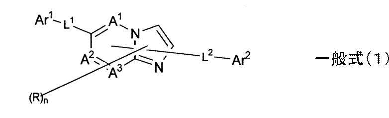
ただし、前記一般式(1)中、A1~A3は、それぞれ独立に、窒素原子又は炭素原子である。Ar1は、置換もしくは無置換の核炭素数6~60のアリール基、又は置換もしくは無置換の核炭素数3~60のヘテロアリール基である。Ar2は、水素原子、置換もしくは無置換の核炭素数6~60のアリール基、置換もしくは無置換の核炭素数3~60のヘテロアリール基、置換もしくは無置換の炭素数1~20のアルキル基、又は置換もしくは無置換の炭素数1~20のアルコキシ基である。ただし、Ar1及びAr2のいずれか一方は、置換もしくは無置換の核炭素数10~60の縮合環基、又は置換もしくは無置換の核炭素数3~60のモノヘテロ縮合環基である。L1及びL2は、それぞれ独立に、単結合、置換もしくは無置換の核炭素数6~60のアリーレン基、置換もしくは無置換の核炭素数3~60のヘテロアリーレン基、又は置換もしくは無置換のフルオレニレン基である。Rは、水素原子、置換もしくは無置換の核炭素数6~60のアリール基、置換もしくは無置換の核炭素数3~60のヘテロアリール基、置換もしくは無置換の炭素数1~20のアルキル基、又は置換もしくは無置換の炭素数1~20のアルコキシ基であり、nは0~5の整数であり、nが2以上の場合、複数のRは同一でも異なっていてもよく、また、隣接する複数のR基同士で結合して、炭素環式脂肪族環又は炭素環式芳香族環を形成していてもよい。

ただし、前記一般式(2)中、X1、X2、X3及びX4は、それぞれ独立に、炭素原子又は窒素原子を表す。X1、X2、X3及びX4のうち、いずれか1つ以上は、窒素原子を表す。X5、X6、X7、X8、X9及びX10は、それぞれ独立に炭素原子又は窒素原子を表す。X11及びX12は、それぞれ独立に、炭素原子又は窒素原子を表し、X13、X14及びX15は、それぞれ独立に、炭素原子、窒素原子、酸素原子、又は硫黄原子を表し、X11、X12、X13、X14及びX15により表される5員環骨格に含まれる窒素原子の数は、2以下である。Lは、単結合又は2価の連結基を表す。
<2> 一般式(1)で表される含窒素複素環誘導体が、下記一般式(3)で表される含窒素複素環誘導体である前記<1>に記載の有機電界発光素子である。
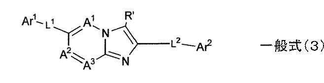
ただし、前記一般式(3)中、A1~A3は、それぞれ独立に、窒素原子又は炭素原子である。Ar1は、置換もしくは無置換の核炭素数6~60のアリール基、又は置換もしくは無置換の核炭素数3~60のヘテロアリール基であり、Ar2は、水素原子、置換もしくは無置換の核炭素数6~60のアリール基、置換もしくは無置換の核炭素数3~60のヘテロアリール基、置換もしくは無置換の炭素数1~20のアルキル基、又は置換もしくは無置換の炭素数1~20のアルコキシ基である。ただし、Ar1及びAr2のいずれか一方は、置換もしくは無置換の核炭素数10~60の縮合環基、又は置換もしくは無置換の核炭素数3~60のモノヘテロ縮合環基である。
L1及びL2は、それぞれ独立に、単結合、置換もしくは無置換の核炭素数6~60のアリーレン基、置換もしくは無置換の核炭素数3~60のヘテロアリーレン基、又は置換もしくは無置換のフルオレニレン基である。
R’は、水素原子、置換もしくは無置換の核炭素数6~60のアリール基、置換もしくは無置換の核炭素数3~60のヘテロアリール基、置換もしくは無置換の炭素数1~20のアルキル基、又は置換もしくは無置換の炭素数1~20のアルコキシ基である。
<3> 一般式(3)で表される含窒素複素環誘導体が、下記一般式(4)で表される含窒素複素環誘導体である前記<2>に記載の有機電界発光素子である。

ただし、前記一般式(4)中、A1及びA2は、それぞれ独立に、窒素原子又は炭素原子である。
Ar1は、置換もしくは無置換の核炭素数6~60のアリール基、又は置換もしくは無置換の核炭素数3~60のヘテロアリール基である。Ar2は、水素原子、置換もしくは無置換の核炭素数6~60のアリール基、置換もしくは無置換の核炭素数3~60のヘテロアリール基、置換もしくは無置換の炭素数1~20のアルキル基、又は置換もしくは無置換の炭素数1~20のアルコキシ基である。ただし、Ar1及びAr2のいずれか一方は、置換もしくは無置換の核炭素数10~60の縮合環基、又は置換もしくは無置換の核炭素数3~60のモノヘテロ縮合環基である。
L1及びL2は、それぞれ独立に、単結合、置換もしくは無置換の核炭素数6~60のアリーレン基、置換もしくは無置換の核炭素数3~60のヘテロアリーレン基、又は置換もしくは無置換のフルオレニレン基である。
R’及びR”は、それぞれ独立に、水素原子、置換もしくは無置換の核炭素数6~60のアリール基、置換もしくは無置換の核炭素数3~60のヘテロアリール基、置換もしくは無置換の炭素数1~20のアルキル基、又は置換もしくは無置換の炭素数1~20のアルコキシ基であり、R’及びR”は同一でも異なっていてもよい。
<4> 一般式(1)、(3)、及び(4)の少なくともいずれかで表される含窒素複素環誘導体において、前記L1及びL2の少なくともいずれかが、下記構造式で表される基から選択される前記<1>から<3>のいずれかに記載の有機電界発光素子である。

<5> 一般式(1)、(3)、及び(4)の少なくともいずれかで表される含窒素複素環誘導体において、Ar1が、下記一般式(5)から(14)のいずれかで表される基である前記<1>から<4>のいずれかに記載の有機電界発光素子である。

ただし、前記式中、R1~R92は、それぞれ独立して、水素原子、ハロゲン原子、置換もしくは無置換の炭素数1~20のアルキル基、置換もしくは無置換の炭素数1~20のアルコキシ基、置換もしくは無置換の核炭素数6~40のアリールオキシ基、置換もしくは無置換の核炭素数12~80のジアリールアミノ基、置換もしくは無置換の核炭素数6~40のアリール基、置換もしくは無置換の核炭素数3~40のヘテロアリール基、又は置換もしくは無置換の核炭素数18~120のジアリールアミノアリール基を表す。L3は、単結合、又は下記構造式で表される置換基を表す。

<6> 一般式(2)で表される化合物が、下記一般式(15)で表される化合物である前記<1>から<5>のいずれかに記載の有機電界発光素子である。

ただし、前記一般式(15)中、X1、X2、X3及びX4は、それぞれ独立に、炭素原子又は窒素原子を表す。X1、X2、X3及びX4のうち、いずれか1つ以上は、窒素原子を表す。R41、R42、R43、R44、R45及びR46は、それぞれ独立に水素原子又は置換基を表す。X11及びX12は、それぞれ独立に、炭素原子又は窒素原子を表し、X13、X14及びX15は、それぞれ独立に、炭素原子、窒素原子、酸素原子、又は硫黄原子を表し、X11、X12、X13、X14及びX15により表される5員環骨格に含まれる窒素原子の数は、2以下である。Lは、単結合又は2価の連結基を表す。
<7> 一般式(15)で表される化合物が、下記一般式(15a-1)で表される化合物である前記<6>に記載の有機電界発光素子である。
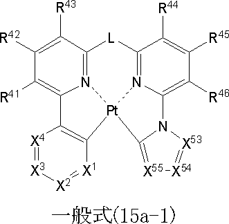
ただし、前記一般式(15a-1)中、X1、X2、X3及びX4は、それぞれ独立に、炭素原子又は窒素原子を表す。X1、X2、X3及びX4のうち、いずれか1つ以上は、窒素原子を表す。R41、R42、R43、R44、R45及びR46は、それぞれ独立に水素原子又は置換基を表す。X53、X54及びX55は、それぞれ独立に、炭素原子又は窒素原子を表し、X53、X54及びX55を含有する5員環骨格に含まれる窒素原子の数は、1又は2である。Lは、単結合又は2価の連結基を表す。
<8> 一般式(15a-1)で表される化合物が、下記一般式(15a-2)で表される化合物である前記<7>に記載の有機電界発光素子である。

ただし、前記一般式(15a-2)中、X1、X2、X3及びX4は、それぞれ独立に、炭素原子又は窒素原子を表す。X1、X2、X3及びX4のうち、いずれか1つ以上は、窒素原子を表す。R41、R42、R43、R44、R45及びR46は、それぞれ独立に水素原子又は置換基を表す。X53及びX54は、それぞれ独立に、炭素原子又は窒素原子を表し、X53及びX54を含有する5員環骨格に含まれる窒素原子の数は、1又は2である。R75は、水素原子又は置換基を表す。Lは、単結合又は2価の連結基を表す。
<9> 一般式(15a-2)で表される化合物が、下記一般式(15a-3)で表される化合物である前記<8>に記載の有機電界発光素子である。

ただし、前記一般式(15a-3)中、X1、X2及びX4は、それぞれ独立に、炭素原子又は窒素原子を表す。R41、R42、R43、R44、R45及びR46は、それぞれ独立に水素原子又は置換基を表す。X53及びX54は、それぞれ独立に、炭素原子又は窒素原子を表し、X53及びX54を含有する5員環骨格に含まれる窒素原子の数は、1又は2である。R75は、水素原子又は置換基を表す。Lは、単結合又は2価の連結基を表す。
<10> 一般式(15)で表される化合物が、下記一般式(15b-1)で表される化合物である前記<6>に記載の有機電界発光素子である。

ただし、前記一般式(15b-1)中、X1、X2、X3及びX4は、それぞれ独立に、炭素原子又は窒素原子を表す。X1、X2、X3及びX4のうち、いずれか1つ以上は、窒素原子を表す。R41、R42、R43、R44、R45及びR46は、それぞれ独立に水素原子又は置換基を表す。X61は、炭素原子又は窒素原子を表す。X13、X14及びX15は、それぞれ独立に、炭素原子、窒素原子、酸素原子、又は硫黄原子を表し、X61、炭素原子、X13、X14及びX15により表される5員環骨格に含まれる窒素原子の数は、2以下である。Lは、単結合又は2価の連結基を表す。
<11> 一般式(15b-1)で表される化合物が、下記一般式(15b-2)で表される化合物である前記<10>に記載の有機電界発光素子である。

ただし、前記一般式(15b-2)中、X1、X2、X3及びX4は、それぞれ独立に、炭素原子又は窒素原子を表す。X1、X2、X3及びX4のうち、いずれか1つ以上は、窒素原子を表す。R41、R42、R43、R44、R45及びR46は、それぞれ独立に水素原子又は置換基を表す。X94及びX95は、それぞれ独立に、炭素原子又は窒素原子を表し、X94及びX95の少なくともいずれか一方は、炭素原子を表す。R93は、水素原子又は置換基を表す。Lは、単結合又は2価の連結基を表す。
<12> 一般式(15b-2)で表される化合物が、下記一般式(15b-3)で表される化合物である前記<11>に記載の有機電界発光素子である。

ただし、前記一般式(15b-3)中、X1、X2及びX4は、それぞれ独立に、炭素原子又は窒素原子を表す。X1、X2及びX4のうち、いずれか1つ以上は、窒素原子を表す。R41、R42、R43、R44、R45及びR46は、それぞれ独立に水素原子又は置換基を表す。X94及びX95は、それぞれ独立に、炭素原子又は窒素原子を表し、X94及びX95の少なくともいずれか一方は、炭素原子を表す。R93は、水素原子又は置換基を表す。Lは、単結合又は2価の連結基を表す。
<13> 一般式(2)で表される部分構造を有する多座配位子の金属錯体化合物、並びに一般式(15)、(15a-1)、(15a-2)、(15a-3)、(15b-1)、(15b-2)、及び(15b-3)で表される四座配位子の白金錯体化合物の少なくとも一種が、発光層に含有される前記<1>から<12>のいずれかに記載の有機電界発光素子である。
<14> 一般式(2)で表される部分構造を有する多座配位子の金属錯体化合物、並びに一般式(15)、(15a-1)、(15a-2)、(15a-3)、(15b-1)、(15b-2)、及び(15b-3)で表される四座配位子の白金錯体化合物の少なくとも一種と、少なくとも一種のホスト材料が、発光層に含有される前記<1>から<13>のいずれかに記載の有機電界発光素子である。
<15> 少なくとも一種のホスト材料が正孔輸送性である前記<14>に記載の有機電界発光素子である。
<16> 含窒素複素環誘導体が、電子注入材料及び電子輸送材料の少なくともいずれかとして用いられている前記<1>から<15>のいずれかに記載の有機電界発光素子である。
<17> 含窒素複素環誘導体を含有する層が、還元性ドーパントを含有する前記<1>から<16>のいずれかに記載の有機電界発光素子である。
<18> 還元性ドーパントが、アルカリ金属、アルカリ土類金属、希土類金属、アルカリ金属の酸化物、アルカリ金属のハロゲン化物、アルカリ土類金属の酸化物、アルカリ土類金属のハロゲン化物、希土類金属の酸化物、希土類金属のハロゲン化物、アルカリ金属の有機錯体、アルカリ土類金属の有機錯体、及び希土類金属の有機錯体から選ばれる少なくとも一種である前記<17>に記載の有機電界発光素子である。 The present invention is based on the above findings by the present inventors, and means for solving the above problems are as follows. That is,
<1> having at least one organic layer including a light emitting layer between an anode and a cathode;
At least one layer in the organic layer contains at least one selected from nitrogen-containing heterocyclic derivatives represented by the following general formula (1), and at least one layer in the organic layer has the following general formula (2) It is an organic electroluminescent element characterized by containing the electron transportable phosphorescence-emitting material represented by this.
However, in the general formula (1), A 1 to A 3 are each independently a nitrogen atom or a carbon atom. Ar 1 is a substituted or unsubstituted aryl group having 6 to 60 nuclear carbon atoms, or a substituted or unsubstituted heteroaryl group having 3 to 60 nuclear carbon atoms. Ar 2 represents a hydrogen atom, a substituted or unsubstituted aryl group having 6 to 60 nuclear carbon atoms, a substituted or unsubstituted heteroaryl group having 3 to 60 nuclear carbon atoms, or a substituted or unsubstituted alkyl group having 1 to 20 carbon atoms. Or a substituted or unsubstituted alkoxy group having 1 to 20 carbon atoms. However, one of Ar 1 and Ar 2 is a substituted or unsubstituted condensed ring group having 10 to 60 nuclear carbon atoms, or a substituted or unsubstituted monoheterocondensed ring group having 3 to 60 nuclear carbon atoms. L 1 and L 2 are each independently a single bond, a substituted or unsubstituted arylene group having 6 to 60 nuclear carbon atoms, a substituted or unsubstituted heteroarylene group having 3 to 60 nuclear carbon atoms, or a substituted or unsubstituted group. Of the fluorenylene group. R represents a hydrogen atom, a substituted or unsubstituted aryl group having 6 to 60 nuclear carbon atoms, a substituted or unsubstituted heteroaryl group having 3 to 60 nuclear carbon atoms, or a substituted or unsubstituted alkyl group having 1 to 20 carbon atoms. Or a substituted or unsubstituted alkoxy group having 1 to 20 carbon atoms, n is an integer of 0 to 5, and when n is 2 or more, a plurality of R may be the same or different and adjacent to each other A plurality of R groups may be bonded to each other to form a carbocyclic aliphatic ring or a carbocyclic aromatic ring.
However, in said general formula (2), X < 1 >, X < 2 >, X < 3 > and X < 4 > represent a carbon atom or a nitrogen atom each independently. Any one or more of X 1 , X 2 , X 3 and X 4 represents a nitrogen atom. X 5 , X 6 , X 7 , X 8 , X 9 and X 10 each independently represent a carbon atom or a nitrogen atom. X 11 and X 12 independently represents a carbon atom or a nitrogen atom, X 13, X 14 and X 15 represent each independently, a carbon atom, a nitrogen atom, an oxygen atom, or a sulfur atom, X 11 , X 12 , X 13 , X 14 and X 15 , the number of nitrogen atoms contained in the 5-membered ring skeleton is 2 or less. L represents a single bond or a divalent linking group.
<2> The organic electroluminescent element according to <1>, wherein the nitrogen-containing heterocyclic derivative represented by the general formula (1) is a nitrogen-containing heterocyclic derivative represented by the following general formula (3).
However, in the general formula (3), A 1 to A 3 are each independently a nitrogen atom or a carbon atom. Ar 1 is a substituted or unsubstituted aryl group having 6 to 60 nuclear carbon atoms, or a substituted or unsubstituted heteroaryl group having 3 to 60 nuclear carbon atoms, and Ar 2 is a hydrogen atom, substituted or unsubstituted An aryl group having 6 to 60 nuclear carbon atoms, a substituted or unsubstituted heteroaryl group having 3 to 60 nuclear carbon atoms, a substituted or unsubstituted alkyl group having 1 to 20 carbon atoms, or a substituted or unsubstituted carbon atom having 1 to 20 alkoxy groups. However, one of Ar 1 and Ar 2 is a substituted or unsubstituted condensed ring group having 10 to 60 nuclear carbon atoms, or a substituted or unsubstituted monoheterocondensed ring group having 3 to 60 nuclear carbon atoms.
L 1 and L 2 are each independently a single bond, a substituted or unsubstituted arylene group having 6 to 60 nuclear carbon atoms, a substituted or unsubstituted heteroarylene group having 3 to 60 nuclear carbon atoms, or a substituted or unsubstituted group. Of the fluorenylene group.
R ′ is a hydrogen atom, a substituted or unsubstituted aryl group having 6 to 60 nuclear carbon atoms, a substituted or unsubstituted heteroaryl group having 3 to 60 nuclear carbon atoms, or a substituted or unsubstituted alkyl group having 1 to 20 carbon atoms. Or a substituted or unsubstituted alkoxy group having 1 to 20 carbon atoms.
<3> The organic electroluminescent element according to <2>, wherein the nitrogen-containing heterocyclic derivative represented by the general formula (3) is a nitrogen-containing heterocyclic derivative represented by the following general formula (4).
However, in the general formula (4), A 1 and A 2 are each independently a nitrogen atom or a carbon atom.
Ar 1 is a substituted or unsubstituted aryl group having 6 to 60 nuclear carbon atoms, or a substituted or unsubstituted heteroaryl group having 3 to 60 nuclear carbon atoms. Ar 2 represents a hydrogen atom, a substituted or unsubstituted aryl group having 6 to 60 nuclear carbon atoms, a substituted or unsubstituted heteroaryl group having 3 to 60 nuclear carbon atoms, or a substituted or unsubstituted alkyl group having 1 to 20 carbon atoms. Or a substituted or unsubstituted alkoxy group having 1 to 20 carbon atoms. However, one of Ar 1 and Ar 2 is a substituted or unsubstituted condensed ring group having 10 to 60 nuclear carbon atoms, or a substituted or unsubstituted monoheterocondensed ring group having 3 to 60 nuclear carbon atoms.
L 1 and L 2 are each independently a single bond, a substituted or unsubstituted arylene group having 6 to 60 nuclear carbon atoms, a substituted or unsubstituted heteroarylene group having 3 to 60 nuclear carbon atoms, or a substituted or unsubstituted group. Of the fluorenylene group.
R ′ and R ″ each independently represents a hydrogen atom, a substituted or unsubstituted aryl group having 6 to 60 nuclear carbon atoms, a substituted or unsubstituted heteroaryl group having 3 to 60 nuclear carbon atoms, substituted or unsubstituted An alkyl group having 1 to 20 carbon atoms, or a substituted or unsubstituted alkoxy group having 1 to 20 carbon atoms, and R ′ and R ″ may be the same or different.
<4> In the nitrogen-containing heterocyclic derivative represented by at least one of the general formulas (1), (3), and (4), at least one of the L 1 and L 2 is represented by the following structural formula. The organic electroluminescence device according to any one of <1> to <3>, wherein the organic electroluminescence device is selected from the following groups.
<5> In the nitrogen-containing heterocyclic derivative represented by at least one of the general formulas (1), (3), and (4), Ar 1 is any one of the following general formulas (5) to (14): It is an organic electroluminescent element in any one of said <1> to <4> which is group represented.
In the above formulae, R 1 to R 92 each independently represents a hydrogen atom, a halogen atom, a substituted or unsubstituted alkyl group having 1 to 20 carbon atoms, or a substituted or unsubstituted alkoxy group having 1 to 20 carbon atoms. Group, substituted or unsubstituted aryloxy group having 6 to 40 nuclear carbon atoms, substituted or unsubstituted diarylamino group having 12 to 80 nuclear carbon atoms, substituted or unsubstituted aryl group having 6 to 40 nuclear carbon atoms, substituted Alternatively, it represents an unsubstituted heteroaryl group having 3 to 40 nuclear carbon atoms, or a substituted or unsubstituted diarylaminoaryl group having 18 to 120 nuclear carbon atoms. L 3 represents a single bond or a substituent represented by the following structural formula.
<6> The organic electroluminescence device according to any one of <1> to <5>, wherein the compound represented by the general formula (2) is a compound represented by the following general formula (15).
However, in said general formula (15), X < 1 >, X < 2 >, X < 3 > and X < 4 > represent a carbon atom or a nitrogen atom each independently. Any one or more of X 1 , X 2 , X 3 and X 4 represents a nitrogen atom. R 41, R 42, R 43 , R 44, R 45 and R 46 each independently represent a hydrogen atom or a substituent. X 11 and X 12 independently represents a carbon atom or a nitrogen atom, X 13, X 14 and X 15 represent each independently, a carbon atom, a nitrogen atom, an oxygen atom, or a sulfur atom, X 11 , X 12 , X 13 , X 14 and X 15 , the number of nitrogen atoms contained in the 5-membered ring skeleton is 2 or less. L represents a single bond or a divalent linking group.
<7> The organic electroluminescence device according to <6>, wherein the compound represented by the general formula (15) is a compound represented by the following general formula (15a-1).
However, in the general formula (15a-1), X 1 , X 2 , X 3 and X 4 each independently represent a carbon atom or a nitrogen atom. Any one or more of X 1 , X 2 , X 3 and X 4 represents a nitrogen atom. R 41, R 42, R 43 , R 44, R 45 and R 46 each independently represent a hydrogen atom or a substituent. X 53 , X 54 and X 55 each independently represent a carbon atom or a nitrogen atom, and the number of nitrogen atoms contained in the 5-membered ring skeleton containing X 53 , X 54 and X 55 is 1 or 2 is there. L represents a single bond or a divalent linking group.
<8> The organic electroluminescence device according to <7>, wherein the compound represented by the general formula (15a-1) is a compound represented by the following general formula (15a-2).
However, in the general formula (15a-2), X 1 , X 2 , X 3 and X 4 each independently represent a carbon atom or a nitrogen atom. Any one or more of X 1 , X 2 , X 3 and X 4 represents a nitrogen atom. R 41, R 42, R 43 , R 44, R 45 and R 46 each independently represent a hydrogen atom or a substituent. X 53 and X 54 each independently represent a carbon atom or a nitrogen atom, and the number of nitrogen atoms contained in the 5-membered ring skeleton containing X 53 and X 54 is 1 or 2. R 75 represents a hydrogen atom or a substituent. L represents a single bond or a divalent linking group.
<9> The organic electroluminescence device according to <8>, wherein the compound represented by the general formula (15a-2) is a compound represented by the following general formula (15a-3).
However, in the general formula (15a-3), X 1 , X 2 and X 4 each independently represent a carbon atom or a nitrogen atom. R 41, R 42, R 43 , R 44, R 45 and R 46 each independently represent a hydrogen atom or a substituent. X 53 and X 54 each independently represent a carbon atom or a nitrogen atom, and the number of nitrogen atoms contained in the 5-membered ring skeleton containing X 53 and X 54 is 1 or 2. R 75 represents a hydrogen atom or a substituent. L represents a single bond or a divalent linking group.
<10> The organic electroluminescence device according to <6>, wherein the compound represented by the general formula (15) is a compound represented by the following general formula (15b-1).
However, in the general formula (15b-1), X 1 , X 2 , X 3 and X 4 each independently represent a carbon atom or a nitrogen atom. Any one or more of X 1 , X 2 , X 3 and X 4 represents a nitrogen atom. R 41, R 42, R 43 , R 44, R 45 and R 46 each independently represent a hydrogen atom or a substituent. X 61 represents a carbon atom or a nitrogen atom. X 13 , X 14 and X 15 each independently represent a carbon atom, a nitrogen atom, an oxygen atom or a sulfur atom, and a 5-membered ring represented by X 61 , carbon atom, X 13 , X 14 and X 15 The number of nitrogen atoms contained in the skeleton is 2 or less. L represents a single bond or a divalent linking group.
<11> The organic electroluminescence device according to <10>, wherein the compound represented by the general formula (15b-1) is a compound represented by the following general formula (15b-2).
However, in the general formula (15b-2), X 1 , X 2 , X 3 and X 4 each independently represent a carbon atom or a nitrogen atom. Any one or more of X 1 , X 2 , X 3 and X 4 represents a nitrogen atom. R 41, R 42, R 43 , R 44, R 45 and R 46 each independently represent a hydrogen atom or a substituent. X94 and X95 each independently represent a carbon atom or a nitrogen atom, and at least one of X94 and X95 represents a carbon atom. R 93 represents a hydrogen atom or a substituent. L represents a single bond or a divalent linking group.
<12> The organic electroluminescence device according to <11>, wherein the compound represented by the general formula (15b-2) is a compound represented by the following general formula (15b-3).
However, in the general formula (15b-3), X 1 , X 2 and X 4 each independently represent a carbon atom or a nitrogen atom. Any one or more of X 1 , X 2 and X 4 represents a nitrogen atom. R 41, R 42, R 43 , R 44, R 45 and R 46 each independently represent a hydrogen atom or a substituent. X94 and X95 each independently represent a carbon atom or a nitrogen atom, and at least one of X94 and X95 represents a carbon atom. R 93 represents a hydrogen atom or a substituent. L represents a single bond or a divalent linking group.
<13> A metal complex compound of a multidentate ligand having a partial structure represented by the general formula (2), and the general formulas (15), (15a-1), (15a-2), (15a-3) , (15b-1), (15b-2) and at least one of the tetradentate platinum complex compounds represented by (15b-3) is contained in the light emitting layer from the above <1> to <12> The organic electroluminescent element according to any one of the above.
<14> A metal complex compound of a polydentate ligand having a partial structure represented by the general formula (2), and the general formulas (15), (15a-1), (15a-2), (15a-3) , (15b-1), (15b-2), and (15b-3) at least one tetradentate platinum complex compound and at least one host material are contained in the light emitting layer. <1> to the organic electroluminescent element according to any one of <13>.
<15> The organic electroluminescence device according to <14>, wherein the at least one host material has hole transportability.
<16> The organic electroluminescent element according to any one of <1> to <15>, wherein the nitrogen-containing heterocyclic derivative is used as at least one of an electron injection material and an electron transport material.
<17> The organic electroluminescence device according to any one of <1> to <16>, wherein the layer containing a nitrogen-containing heterocyclic derivative contains a reducing dopant.
<18> The reducing dopant is alkali metal, alkaline earth metal, rare earth metal, alkali metal oxide, alkali metal halide, alkaline earth metal oxide, alkaline earth metal halide, rare earth metal The organic electroluminescence device according to <17>, wherein the organic electroluminescence device is at least one selected from oxides, halides of rare earth metals, organic complexes of alkali metals, organic complexes of alkaline earth metals, and organic complexes of rare earth metals.
本発明の有機電界発光素子は、陽極と陰極の間に、発光層を含む少なくとも一層の有機層を有してなり、
前記有機層における少なくとも1層が、特定の含窒素複素環誘導体から選択される少なくとも1種を含有し、かつ前記有機層における少なくとも1層が、特定の電子輸送性燐光発光材料を含有する。 (Organic electroluminescent device)
The organic electroluminescent element of the present invention comprises at least one organic layer including a light emitting layer between an anode and a cathode,
At least one layer in the organic layer contains at least one selected from a specific nitrogen-containing heterocyclic derivative, and at least one layer in the organic layer contains a specific electron-transporting phosphorescent material.
前記含窒素複素環誘導体としては、下記一般式(1)で表される含窒素複素環誘導体から選択される少なくとも1種を含有する。

ただし、前記一般式(1)中、A1~A3は、それぞれ独立に、窒素原子又は炭素原子である。Ar1は、置換もしくは無置換の核炭素数6~60のアリール基、又は置換もしくは無置換の核炭素数3~60のヘテロアリール基である。Ar2は、水素原子、置換もしくは無置換の核炭素数6~60のアリール基、置換もしくは無置換の核炭素数3~60のヘテロアリール基、置換もしくは無置換の炭素数1~20のアルキル基、又は置換もしくは無置換の炭素数1~20のアルコキシ基である。ただし、Ar1及びAr2のいずれか一方は、置換もしくは無置換の核炭素数10~60の縮合環基、又は置換もしくは無置換の核炭素数3~60のモノヘテロ縮合環基である。L1及びL2は、それぞれ独立に、単結合、置換もしくは無置換の核炭素数6~60のアリーレン基、置換もしくは無置換の核炭素数3~60のヘテロアリーレン基、又は置換もしくは無置換のフルオレニレン基である。Rは、水素原子、置換もしくは無置換の核炭素数6~60のアリール基、置換もしくは無置換の核炭素数3~60のヘテロアリール基、置換もしくは無置換の炭素数1~20のアルキル基、又は置換もしくは無置換の炭素数1~20のアルコキシ基であり、nは0~5の整数であり、nが2以上の場合、複数のRは同一でも異なっていてもよく、また、隣接する複数のR基同士で結合して、炭素環式脂肪族環又は炭素環式芳香族環を形成していてもよい。 <Nitrogen-containing heterocyclic derivatives>
The nitrogen-containing heterocyclic derivative contains at least one selected from nitrogen-containing heterocyclic derivatives represented by the following general formula (1).
However, in the general formula (1), A 1 to A 3 are each independently a nitrogen atom or a carbon atom. Ar 1 is a substituted or unsubstituted aryl group having 6 to 60 nuclear carbon atoms, or a substituted or unsubstituted heteroaryl group having 3 to 60 nuclear carbon atoms. Ar 2 represents a hydrogen atom, a substituted or unsubstituted aryl group having 6 to 60 nuclear carbon atoms, a substituted or unsubstituted heteroaryl group having 3 to 60 nuclear carbon atoms, or a substituted or unsubstituted alkyl group having 1 to 20 carbon atoms. Or a substituted or unsubstituted alkoxy group having 1 to 20 carbon atoms. However, one of Ar 1 and Ar 2 is a substituted or unsubstituted condensed ring group having 10 to 60 nuclear carbon atoms, or a substituted or unsubstituted monoheterocondensed ring group having 3 to 60 nuclear carbon atoms. L 1 and L 2 are each independently a single bond, a substituted or unsubstituted arylene group having 6 to 60 nuclear carbon atoms, a substituted or unsubstituted heteroarylene group having 3 to 60 nuclear carbon atoms, or a substituted or unsubstituted group. Of the fluorenylene group. R represents a hydrogen atom, a substituted or unsubstituted aryl group having 6 to 60 nuclear carbon atoms, a substituted or unsubstituted heteroaryl group having 3 to 60 nuclear carbon atoms, or a substituted or unsubstituted alkyl group having 1 to 20 carbon atoms. Or a substituted or unsubstituted alkoxy group having 1 to 20 carbon atoms, n is an integer of 0 to 5, and when n is 2 or more, a plurality of R may be the same or different and adjacent to each other A plurality of R groups may be bonded to each other to form a carbocyclic aliphatic ring or a carbocyclic aromatic ring.

ただし、前記一般式(3)中、A1~A3は、それぞれ独立に、窒素原子又は炭素原子である。Ar1は、置換もしくは無置換の核炭素数6~60のアリール基、又は置換もしくは無置換の核炭素数3~60のヘテロアリール基であり、Ar2は、水素原子、置換もしくは無置換の核炭素数6~60のアリール基、置換もしくは無置換の核炭素数3~60のヘテロアリール基、置換もしくは無置換の炭素数1~20のアルキル基、又は置換もしくは無置換の炭素数1~20のアルコキシ基である。ただし、Ar1及びAr2のいずれか一方は、置換もしくは無置換の核炭素数10~60の縮合環基、又は置換もしくは無置換の核炭素数3~60のモノヘテロ縮合環基である。
L1及びL2は、それぞれ独立に、単結合、置換もしくは無置換の核炭素数6~60のアリーレン基、置換もしくは無置換の核炭素数3~60のヘテロアリーレン基、又は置換もしくは無置換のフルオレニレン基である。
R’は、水素原子、置換もしくは無置換の核炭素数6~60のアリール基、置換もしくは無置換の核炭素数3~60のヘテロアリール基、置換もしくは無置換の炭素数1~20のアルキル基、又は置換もしくは無置換の炭素数1~20のアルコキシ基である。 The nitrogen-containing heterocyclic derivative represented by the general formula (1) is preferably a nitrogen-containing heterocyclic derivative represented by the following general formula (3).
However, in the general formula (3), A 1 to A 3 are each independently a nitrogen atom or a carbon atom. Ar 1 is a substituted or unsubstituted aryl group having 6 to 60 nuclear carbon atoms, or a substituted or unsubstituted heteroaryl group having 3 to 60 nuclear carbon atoms, and Ar 2 is a hydrogen atom, substituted or unsubstituted An aryl group having 6 to 60 nuclear carbon atoms, a substituted or unsubstituted heteroaryl group having 3 to 60 nuclear carbon atoms, a substituted or unsubstituted alkyl group having 1 to 20 carbon atoms, or a substituted or unsubstituted carbon atom having 1 to 20 alkoxy groups. However, one of Ar 1 and Ar 2 is a substituted or unsubstituted condensed ring group having 10 to 60 nuclear carbon atoms, or a substituted or unsubstituted monoheterocondensed ring group having 3 to 60 nuclear carbon atoms.
L 1 and L 2 are each independently a single bond, a substituted or unsubstituted arylene group having 6 to 60 nuclear carbon atoms, a substituted or unsubstituted heteroarylene group having 3 to 60 nuclear carbon atoms, or a substituted or unsubstituted group. Of the fluorenylene group.
R ′ is a hydrogen atom, a substituted or unsubstituted aryl group having 6 to 60 nuclear carbon atoms, a substituted or unsubstituted heteroaryl group having 3 to 60 nuclear carbon atoms, or a substituted or unsubstituted alkyl group having 1 to 20 carbon atoms. Or a substituted or unsubstituted alkoxy group having 1 to 20 carbon atoms.

ただし、前記一般式(4)中、A1及びA2は、それぞれ独立に、窒素原子又は炭素原子である。
Ar1は、置換もしくは無置換の核炭素数6~60のアリール基、又は置換もしくは無置換の核炭素数3~60のヘテロアリール基である。Ar2は、水素原子、置換もしくは無置換の核炭素数6~60のアリール基、置換もしくは無置換の核炭素数3~60のヘテロアリール基、置換もしくは無置換の炭素数1~20のアルキル基、又は置換もしくは無置換の炭素数1~20のアルコキシ基である。ただし、Ar1及びAr2のいずれか一方は、置換もしくは無置換の核炭素数10~60の縮合環基、又は置換もしくは無置換の核炭素数3~60のモノヘテロ縮合環基である。
L1及びL2は、それぞれ独立に、単結合、置換もしくは無置換の核炭素数6~60のアリーレン基、置換もしくは無置換の核炭素数3~60のヘテロアリーレン基、又は置換もしくは無置換のフルオレニレン基である。
R’及びR”は、それぞれ独立に、水素原子、置換もしくは無置換の核炭素数6~60のアリール基、置換もしくは無置換の核炭素数3~60のヘテロアリール基、置換もしくは無置換の炭素数1~20のアルキル基、又は置換もしくは無置換の炭素数1~20のアルコキシ基であり、R’及びR”は同一でも異なっていてもよい。 The nitrogen-containing heterocyclic derivative represented by the general formula (3) is preferably a nitrogen-containing heterocyclic derivative represented by the following general formula (4).
However, in the general formula (4), A 1 and A 2 are each independently a nitrogen atom or a carbon atom.
Ar 1 is a substituted or unsubstituted aryl group having 6 to 60 nuclear carbon atoms, or a substituted or unsubstituted heteroaryl group having 3 to 60 nuclear carbon atoms. Ar 2 represents a hydrogen atom, a substituted or unsubstituted aryl group having 6 to 60 nuclear carbon atoms, a substituted or unsubstituted heteroaryl group having 3 to 60 nuclear carbon atoms, or a substituted or unsubstituted alkyl group having 1 to 20 carbon atoms. Or a substituted or unsubstituted alkoxy group having 1 to 20 carbon atoms. However, one of Ar 1 and Ar 2 is a substituted or unsubstituted condensed ring group having 10 to 60 nuclear carbon atoms, or a substituted or unsubstituted monoheterocondensed ring group having 3 to 60 nuclear carbon atoms.
L 1 and L 2 are each independently a single bond, a substituted or unsubstituted arylene group having 6 to 60 nuclear carbon atoms, a substituted or unsubstituted heteroarylene group having 3 to 60 nuclear carbon atoms, or a substituted or unsubstituted group. Of the fluorenylene group.
R ′ and R ″ each independently represents a hydrogen atom, a substituted or unsubstituted aryl group having 6 to 60 nuclear carbon atoms, a substituted or unsubstituted heteroaryl group having 3 to 60 nuclear carbon atoms, substituted or unsubstituted An alkyl group having 1 to 20 carbon atoms, or a substituted or unsubstituted alkoxy group having 1 to 20 carbon atoms, and R ′ and R ″ may be the same or different.

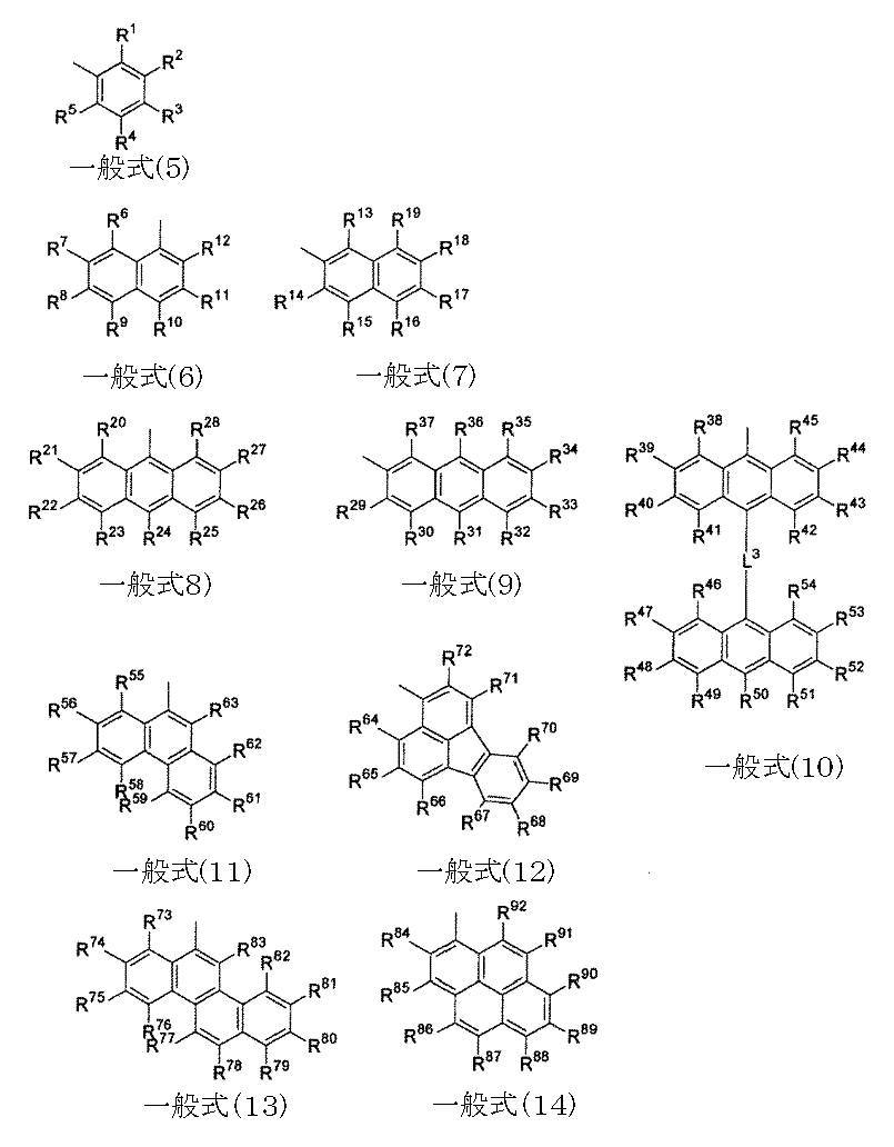
ただし、前記式中、R1~R92は、それぞれ独立して、水素原子、ハロゲン原子、置換もしくは無置換の炭素数1~20のアルキル基、置換もしくは無置換の炭素数1~20のアルコキシ基、置換もしくは無置換の核炭素数6~40のアリールオキシ基、置換もしくは無置換の核炭素数12~80のジアリールアミノ基、置換もしくは無置換の核炭素数6~40のアリール基、置換もしくは無置換の核炭素数3~40のヘテロアリール基、又は置換もしくは無置換の核炭素数18~120のジアリールアミノアリール基を表す。L3は、単結合、又は下記構造式で表される置換基を表す。

In the above formulae, R 1 to R 92 each independently represents a hydrogen atom, a halogen atom, a substituted or unsubstituted alkyl group having 1 to 20 carbon atoms, or a substituted or unsubstituted alkoxy group having 1 to 20 carbon atoms. Group, substituted or unsubstituted aryloxy group having 6 to 40 nuclear carbon atoms, substituted or unsubstituted diarylamino group having 12 to 80 nuclear carbon atoms, substituted or unsubstituted aryl group having 6 to 40 nuclear carbon atoms, substituted Alternatively, it represents an unsubstituted heteroaryl group having 3 to 40 nuclear carbon atoms, or a substituted or unsubstituted diarylaminoaryl group having 18 to 120 nuclear carbon atoms. L 3 represents a single bond or a substituent represented by the following structural formula.

前記含窒素複素環誘導体は、有機層における少なくとも1層に含有されるが、電子注入層及び電子輸送層の少なくともいずれかが好ましい。
前記電子注入層及び電子輸送層は、陰極又は陰極側から電子を受け取り陽極側に輸送する機能を有する層である。 The nitrogen-containing heterocyclic derivative is preferably used as at least one of an electron injection material and an electron transport material.
The nitrogen-containing heterocyclic derivative is contained in at least one layer in the organic layer, and at least one of an electron injection layer and an electron transport layer is preferable.
The electron injection layer and the electron transport layer are layers having a function of receiving electrons from the cathode or the cathode side and transporting them to the anode side.
前記還元性ドーパントとしては、アルカリ金属、アルカリ土類金属、希土類金属、アルカリ金属の酸化物、アルカリ金属のハロゲン化物、アルカリ土類金属の酸化物、アルカリ土類金属のハロゲン化物、希土類金属の酸化物、希土類金属のハロゲン化物、アルカリ金属の有機錯体、アルカリ土類金属の有機錯体、及び希土類金属の有機錯体から選ばれる少なくとも一種であることが好ましい。
前記還元性ドーパントの使用量は、材料の種類によって異なるが、電子輸送層材料又は電子注入層材料に対して0.1質量%~99質量%であることが好ましく、0.3質量%~80質量%であることがより好ましく、0.5質量%~50質量%であることが更に好ましい。 The layer (organic layer, electron injection layer, electron transport layer) containing the nitrogen-containing heterocyclic derivative preferably contains a reducing dopant.
Examples of the reducing dopant include alkali metal, alkaline earth metal, rare earth metal, alkali metal oxide, alkali metal halide, alkaline earth metal oxide, alkaline earth metal halide, rare earth metal oxidation. And at least one selected from a rare earth metal halide, an alkali metal organic complex, an alkaline earth metal organic complex, and a rare earth metal organic complex.
The amount of the reducing dopant used varies depending on the type of material, but is preferably 0.1% by mass to 99% by mass, and preferably 0.3% by mass to 80% by mass with respect to the electron transport layer material or the electron injection layer material. More preferably, it is more preferably 0.5% by mass to 50% by mass.
前記電子輸送層の厚みは、1nm~200nmであることが好ましく、1nm~100nmであることがより好ましいく、1nm~50nmであることが更に好ましい。
前記電子注入層の厚みは、1nm~200nmが好ましく、1nm~100nmがより好ましいく、1nm~50nmであることが更に好ましい。 The electron transport layer and the electron injection layer can be formed according to a known method. For example, a vapor deposition method, a wet film forming method, an MBE (molecular beam epitaxy) method, a cluster ion beam method, a molecular stacking method, an LB method. It can be suitably formed by a printing method, a transfer method, or the like.
The thickness of the electron transport layer is preferably 1 nm to 200 nm, more preferably 1 nm to 100 nm, and even more preferably 1 nm to 50 nm.
The thickness of the electron injection layer is preferably 1 nm to 200 nm, more preferably 1 nm to 100 nm, and even more preferably 1 nm to 50 nm.
前記電子輸送性燐光発光材料としては、下記一般式(2)で表される電子輸送性燐光発光材料を含有することが好ましい。
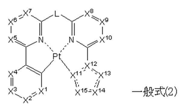
ただし、前記一般式(2)中、X1、X2、X3及びX4は、それぞれ独立に、炭素原子又は窒素原子を表す。X1、X2、X3及びX4のうち、いずれか1つ以上は、窒素原子を表す。X5、X6、X7、X8、X9及びX10は、それぞれ独立に炭素原子又は窒素原子を表す。X11及びX12は、それぞれ独立に、炭素原子又は窒素原子を表し、X13、X14及びX15は、それぞれ独立に、炭素原子、窒素原子、酸素原子、又は硫黄原子を表し、X11、X12、X13、X14及びX15により表される5員環骨格に含まれる窒素原子の数は、2以下である。Lは、単結合又は2価の連結基を表す。 <Electron transporting phosphorescent material>
The electron-transporting phosphorescent material preferably contains an electron-transporting phosphorescent material represented by the following general formula (2).
However, in said general formula (2), X < 1 >, X < 2 >, X < 3 > and X < 4 > represent a carbon atom or a nitrogen atom each independently. Any one or more of X 1 , X 2 , X 3 and X 4 represents a nitrogen atom. X 5 , X 6 , X 7 , X 8 , X 9 and X 10 each independently represent a carbon atom or a nitrogen atom. X 11 and X 12 independently represents a carbon atom or a nitrogen atom, X 13, X 14 and X 15 represent each independently, a carbon atom, a nitrogen atom, an oxygen atom, or a sulfur atom, X 11 , X 12 , X 13 , X 14 and X 15 , the number of nitrogen atoms contained in the 5-membered ring skeleton is 2 or less. L represents a single bond or a divalent linking group.

ただし、前記一般式(15)中、X1、X2、X3及びX4は、それぞれ独立に、炭素原子又は窒素原子を表す。X1、X2、X3及びX4のうち、いずれか1つ以上は、窒素原子を表す。R41、R42、R43、R44、R45及びR46は、それぞれ独立に水素原子又は置換基を表す。X11及びX12は、それぞれ独立に、炭素原子又は窒素原子を表し、X13、X14及びX15は、それぞれ独立に、炭素原子、窒素原子、酸素原子、又は硫黄原子を表し、X11、X12、X13、X14及びX15により表される5員環骨格に含まれる窒素原子の数は、2以下である。Lは、単結合又は2価の連結基を表す。 The compound represented by the general formula (2) is preferably a compound represented by the following general formula (15).
However, in said general formula (15), X < 1 >, X < 2 >, X < 3 > and X < 4 > represent a carbon atom or a nitrogen atom each independently. Any one or more of X 1 , X 2 , X 3 and X 4 represents a nitrogen atom. R 41, R 42, R 43 , R 44, R 45 and R 46 each independently represent a hydrogen atom or a substituent. X 11 and X 12 independently represents a carbon atom or a nitrogen atom, X 13, X 14 and X 15 represent each independently, a carbon atom, a nitrogen atom, an oxygen atom, or a sulfur atom, X 11 , X 12 , X 13 , X 14 and X 15 , the number of nitrogen atoms contained in the 5-membered ring skeleton is 2 or less. L represents a single bond or a divalent linking group.

ただし、前記一般式(15a-1)中、X1、X2、X3及びX4は、それぞれ独立に、炭素原子又は窒素原子を表す。X1、X2、X3及びX4のうち、いずれか1つ以上は、窒素原子を表す。R41、R42、R43、R44、R45及びR46は、それぞれ独立に水素原子又は置換基を表す。X53、X54及びX55は、それぞれ独立に、炭素原子又は窒素原子を表し、X53、X54及びX55を含有する5員環骨格に含まれる窒素原子の数は、1又は2である。Lは、単結合又は2価の連結基を表す。 The compound represented by the general formula (15) is preferably a compound represented by the following general formula (15a-1).
However, in the general formula (15a-1), X 1 , X 2 , X 3 and X 4 each independently represent a carbon atom or a nitrogen atom. Any one or more of X 1 , X 2 , X 3 and X 4 represents a nitrogen atom. R 41, R 42, R 43 , R 44, R 45 and R 46 each independently represent a hydrogen atom or a substituent. X 53 , X 54 and X 55 each independently represent a carbon atom or a nitrogen atom, and the number of nitrogen atoms contained in the 5-membered ring skeleton containing X 53 , X 54 and X 55 is 1 or 2 is there. L represents a single bond or a divalent linking group.

ただし、前記一般式(15a-2)中、X1、X2、X3及びX4は、それぞれ独立に、炭素原子又は窒素原子を表す。X1、X2、X3及びX4のうち、いずれか1つ以上は、窒素原子を表す。R41、R42、R43、R44、R45及びR46は、それぞれ独立に水素原子又は置換基を表す。X53及びX54は、それぞれ独立に、炭素原子又は窒素原子を表し、X53及びX54を含有する5員環骨格に含まれる窒素原子の数は、1又は2である。R75は、水素原子又は置換基を表す。Lは、単結合又は2価の連結基を表す。 The compound represented by the general formula (15a-1) is preferably a compound represented by the following general formula (15a-2).
However, in the general formula (15a-2), X 1 , X 2 , X 3 and X 4 each independently represent a carbon atom or a nitrogen atom. Any one or more of X 1 , X 2 , X 3 and X 4 represents a nitrogen atom. R 41, R 42, R 43 , R 44, R 45 and R 46 each independently represent a hydrogen atom or a substituent. X 53 and X 54 each independently represent a carbon atom or a nitrogen atom, and the number of nitrogen atoms contained in the 5-membered ring skeleton containing X 53 and X 54 is 1 or 2. R 75 represents a hydrogen atom or a substituent. L represents a single bond or a divalent linking group.
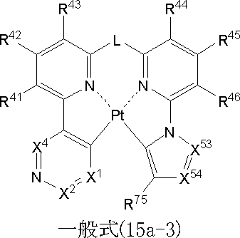
ただし、前記一般式(15a-3)中、X1、X2及びX4は、それぞれ独立に、炭素原子又は窒素原子を表す。R41、R42、R43、R44、R45及びR46は、それぞれ独立に水素原子又は置換基を表す。X53及びX54は、それぞれ独立に、炭素原子又は窒素原子を表し、X53及びX54を含有する5員環骨格に含まれる窒素原子の数は、1又は2である。R75は、水素原子又は置換基を表す。Lは、単結合又は2価の連結基を表す。 The compound represented by the general formula (15a-2) is preferably a compound represented by the following general formula (15a-3).
However, in the general formula (15a-3), X 1 , X 2 and X 4 each independently represent a carbon atom or a nitrogen atom. R 41, R 42, R 43 , R 44, R 45 and R 46 each independently represent a hydrogen atom or a substituent. X 53 and X 54 each independently represent a carbon atom or a nitrogen atom, and the number of nitrogen atoms contained in the 5-membered ring skeleton containing X 53 and X 54 is 1 or 2. R 75 represents a hydrogen atom or a substituent. L represents a single bond or a divalent linking group.
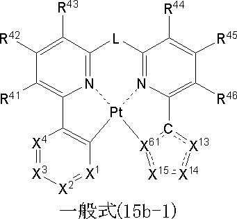
ただし、前記一般式(15b-1)中、X1、X2、X3及びX4は、それぞれ独立に、炭素原子又は窒素原子を表す。X1、X2、X3及びX4のうち、いずれか1つ以上は、窒素原子を表す。R41、R42、R43、R44、R45及びR46は、それぞれ独立に水素原子又は置換基を表す。X61は、炭素原子又は窒素原子を表す。X13、X14及びX15は、それぞれ独立に、炭素原子、窒素原子、酸素原子、又は硫黄原子を表し、X61、炭素原子、X13、X14及びX15により表される5員環骨格に含まれる窒素原子の数は、2以下である。Lは、単結合又は2価の連結基を表す。 The compound represented by the general formula (15) is preferably a compound represented by the following general formula (15b-1).
However, in the general formula (15b-1), X 1 , X 2 , X 3 and X 4 each independently represent a carbon atom or a nitrogen atom. Any one or more of X 1 , X 2 , X 3 and X 4 represents a nitrogen atom. R 41, R 42, R 43 , R 44, R 45 and R 46 each independently represent a hydrogen atom or a substituent. X 61 represents a carbon atom or a nitrogen atom. X 13 , X 14 and X 15 each independently represent a carbon atom, a nitrogen atom, an oxygen atom or a sulfur atom, and a 5-membered ring represented by X 61 , carbon atom, X 13 , X 14 and X 15 The number of nitrogen atoms contained in the skeleton is 2 or less. L represents a single bond or a divalent linking group.

ただし、前記一般式(15b-2)中、X1、X2、X3及びX4は、それぞれ独立に、炭素原子又は窒素原子を表す。X1、X2、X3及びX4のうち、いずれか1つ以上は、窒素原子を表す。R41、R42、R43、R44、R45及びR46は、それぞれ独立に水素原子又は置換基を表す。X94及びX95は、それぞれ独立に、炭素原子又は窒素原子を表し、X94及びX95の少なくともいずれか一方は、炭素原子を表す。R93は、水素原子又は置換基を表す。Lは、単結合又は2価の連結基を表す。 The compound represented by the general formula (15b-1) is preferably a compound represented by the following general formula (15b-2).
However, in the general formula (15b-2), X 1 , X 2 , X 3 and X 4 each independently represent a carbon atom or a nitrogen atom. Any one or more of X 1 , X 2 , X 3 and X 4 represents a nitrogen atom. R 41, R 42, R 43 , R 44, R 45 and R 46 each independently represent a hydrogen atom or a substituent. X94 and X95 each independently represent a carbon atom or a nitrogen atom, and at least one of X94 and X95 represents a carbon atom. R 93 represents a hydrogen atom or a substituent. L represents a single bond or a divalent linking group.

ただし、前記一般式(15b-3)中、X1、X2及びX4は、それぞれ独立に、炭素原子又は窒素原子を表す。X1、X2及びX4のうち、いずれか1つ以上は、窒素原子を表す。R41、R42、R43、R44、R45及びR46は、それぞれ独立に水素原子又は置換基を表す。X94及びX95は、それぞれ独立に、炭素原子又は窒素原子を表し、X94及びX95の少なくともいずれか一方は、炭素原子を表す。R93は、水素原子又は置換基を表す。Lは、単結合又は2価の連結基を表す。 The compound represented by the general formula (15b-2) is preferably a compound represented by the following general formula (15b-3).
However, in the general formula (15b-3), X 1 , X 2 and X 4 each independently represent a carbon atom or a nitrogen atom. Any one or more of X 1 , X 2 and X 4 represents a nitrogen atom. R 41, R 42, R 43 , R 44, R 45 and R 46 each independently represent a hydrogen atom or a substituent. X94 and X95 each independently represent a carbon atom or a nitrogen atom, and at least one of X94 and X95 represents a carbon atom. R 93 represents a hydrogen atom or a substituent. L represents a single bond or a divalent linking group.
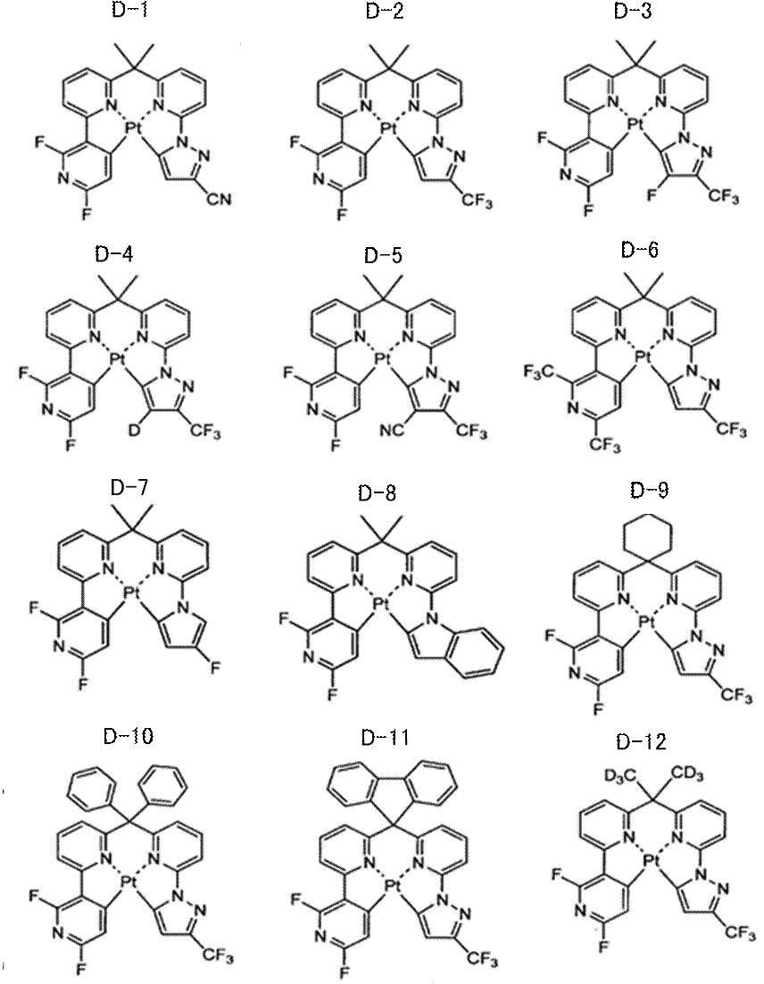


この場合、前記発光性ドーパントとしての電子輸送性燐光発光材料の含有量は、発光層中に一般的に発光層を形成する全化合物質量に対して、0.1質量%~90質量%であることが好ましく、1質量%~50質量%がより好ましく、1質量%~25質量%が更に好ましい。 A metal complex compound of a polydentate ligand having a partial structure represented by the general formula (2), and the general formulas (15), (15a-1), (15a-2), (15a-3), ( It is preferable that at least one of the tetradentate platinum complex compounds represented by 15b-1), (15b-2), and (15b-3) and at least one host material are contained in the light emitting layer. Additives such as adamantane may also be included.
In this case, the content of the electron transporting phosphorescent light emitting material as the light emitting dopant is generally 0.1% by mass to 90% by mass with respect to the total mass of the compound forming the light emitting layer in the light emitting layer. It is preferably 1% by mass to 50% by mass, more preferably 1% by mass to 25% by mass.
本発明に用いられる電子輸送性ホスト材料としては、耐久性向上、駆動電圧低下の観点から、電子親和力Eaが2.5eV以上3.5eV以下であることが好ましく、2.6eV以上3.4eV以下であることがより好ましく、2.8eV以上3.3eV以下であることが更に好ましい。また、耐久性向上、駆動電圧低下の観点から、イオン化ポテンシャルIpが5.7eV以上7.5eV以下であることが好ましく、5.8eV以上7.0eV以下であることがより好ましく、5.9eV以上6.5eV以下であることが更に好ましい。
好ましい最低三重項励起準位(以下T1とする)は好ましくは2.2eV以上3.7eV以下であり、更に好ましくは2.4eV以上3.7eV以下であり、最も好ましくは2.4eV以上3.4eV以下である。
このような電子輸送性ホストとしては、具体的には、ピリジン、ピリミジン、トリアジン、イミダゾール、ピラゾール、トリアゾ-ル、オキサゾ-ル、オキサジアゾ-ル、フルオレノン、アントラキノジメタン、アントロン、ジフェニルキノン、チオピランジオキシド、カルボジイミド、フルオレニリデンメタン、ジスチリルピラジン、フッ素置換芳香族化合物、ナフタレン、ペリレン等の芳香環テトラカルボン酸無水物、フタロシアニン、及びそれらの誘導体(他の環と縮合環を形成してもよい)、8-キノリノ-ル誘導体の金属錯体やメタルフタロシアニン、ベンゾオキサゾ-ルやベンゾチアゾ-ルを配位子とする金属錯体に代表される各種金属錯体等を挙げることができる。 <Electron transporting host material>
The electron transporting host material used in the present invention preferably has an electron affinity Ea of 2.5 eV or more and 3.5 eV or less, from the viewpoint of improving durability and lowering driving voltage, and 2.6 eV or more and 3.4 eV or less. It is more preferable that it is 2.8 eV or more and 3.3 eV or less. Further, from the viewpoint of improving durability and reducing driving voltage, the ionization potential Ip is preferably 5.7 eV or more and 7.5 eV or less, more preferably 5.8 eV or more and 7.0 eV or less, and 5.9 eV or more. More preferably, it is 6.5 eV or less.
A preferable lowest triplet excited level (hereinafter referred to as T1) is preferably 2.2 eV or more and 3.7 eV or less, more preferably 2.4 eV or more and 3.7 eV or less, and most preferably 2.4 eV or more and 3. 4 eV or less.
Specific examples of such an electron transporting host include pyridine, pyrimidine, triazine, imidazole, pyrazole, triazole, oxazole, oxadiazol, fluorenone, anthraquinodimethane, anthrone, diphenylquinone, thiol. Pyrandoxide, carbodiimide, fluorenylidenemethane, distyrylpyrazine, fluorinated aromatic compounds, aromatic tetracarboxylic anhydrides such as naphthalene and perylene, phthalocyanines, and their derivatives (form condensed rings with other rings) And metal complexes of 8-quinolinol derivatives, metal phthalocyanines, metal complexes having benzoxazole or benzothiazol as ligands, and the like.
金属錯体中の金属イオンは特に限定されないが、好ましくはベリリウムイオン、マグネシウムイオン、アルミニウムイオン、ガリウムイオン、亜鉛イオン、インジウムイオン、錫イオン、白金イオン、又はパラジウムイオンであり、より好ましくはベリリウムイオン、アルミニウムイオン、ガリウムイオン、亜鉛イオン、白金イオン、又はパラジウムイオンであり、更に好ましくはアルミニウムイオン、亜鉛イオン、白金イオン、又はパラジウムイオンである。 Preferred examples of the electron transporting host include metal complexes, azole derivatives (benzimidazole derivatives, imidazopyridine derivatives, etc.), and azine derivatives (pyridine derivatives, pyrimidine derivatives, triazine derivatives, etc.). To metal complex compounds are preferred. The metal complex compound is more preferably a metal complex having a ligand having at least one nitrogen atom, oxygen atom or sulfur atom coordinated to the metal.
The metal ion in the metal complex is not particularly limited, but is preferably beryllium ion, magnesium ion, aluminum ion, gallium ion, zinc ion, indium ion, tin ion, platinum ion, or palladium ion, more preferably beryllium ion, Aluminum ion, gallium ion, zinc ion, platinum ion, or palladium ion, and more preferably aluminum ion, zinc ion, platinum ion, or palladium ion.
配位子としては、例えばアジン配位子(例えば、ピリジン配位子、ビピリジル配位子、ターピリジン配位子などが挙げられる。)、ヒドロキシフェニルアゾール配位子(例えば、ヒドロキシフェニルベンズイミダゾール配位子、ヒドロキシフェニルベンズオキサゾール配位子、ヒドロキシフェニルイミダゾール配位子、ヒドロキシフェニルイミダゾピリジン配位子などが挙げられる。)、アルコキシ配位子(好ましくは炭素数1~30、より好ましくは炭素数1~20、特に好ましくは炭素数1~10であり、例えばメトキシ、エトキシ、ブトキシ、2-エチルヘキシロキシなどが挙げられる。)、アリールオキシ配位子(好ましくは炭素数6~30、より好ましくは炭素数6~20、特に好ましくは炭素数6~12であり、例えばフェニルオキシ、1-ナフチルオキシ、2-ナフチルオキシ、2,4,6-トリメチルフェニルオキシ、4-ビフェニルオキシなどが挙げられる。)、ヘテロアリールオキシ配位子(好ましくは炭素数1~30、より好ましくは炭素数1~20、特に好ましくは炭素数1~12であり、例えばピリジルオキシ、ピラジルオキシ、ピリミジルオキシ、キノリルオキシなどが挙げられる。)、アルキルチオ配位子(好ましくは炭素数1~30、より好ましくは炭素数1~20、特に好ましくは炭素数1~12であり、例えばメチルチオ、エチルチオなどが挙げられる。)、アリールチオ配位子(好ましくは炭素数6~30、より好ましくは炭素数6~20、特に好ましくは炭素数6~12であり、例えばフェニルチオなどが挙げられる。)、ヘテロアリールチオ配位子(好ましくは炭素数1~30、より好ましくは炭素数1~20、特に好ましくは炭素数1~12であり、例えばピリジルチオ、2-ベンズイミゾリルチオ、2-ベンズオキサゾリルチオ、2-ベンズチアゾリルチオなどが挙げられる。)、シロキシ配位子(好ましくは炭素数1~30、より好ましくは炭素数3~25、特に好ましくは炭素数6~20であり、例えば、トリフェニルシロキシ基、トリエトキシシロキシ基、トリイソプロピルシロキシ基などが挙げられる。)、芳香族炭化水素アニオン配位子(好ましくは炭素数6~30、より好ましくは炭素数6~25、特に好ましくは炭素数6~20であり、例えばフェニルアニオン、ナフチルアニオン、アントラニルアニオンなどが挙げられる。)、芳香族ヘテロ環アニオン配位子(好ましくは炭素数1~30、より好ましくは炭素数2~25、特に好ましくは炭素数2~20であり、例えばピロールアニオン、ピラゾールアニオン、ピラゾールアニオン、トリアゾールアニオン、オキサゾールアニオン、ベンゾオキサゾールアニオン、チアゾールアニオン、ベンゾチアゾールアニオン、チオフェンアニオン、ベンゾチオフェンアニオンなどが挙げられる。)、インドレニンアニオン配位子などが挙げられ、好ましくは含窒素ヘテロ環配位子、アリールオキシ配位子、ヘテロアリールオキシ基、又はシロキシ配位子であり、更に好ましくは含窒素ヘテロ環配位子、アリールオキシ配位子、シロキシ配位子、芳香族炭化水素アニオン配位子、又は芳香族ヘテロ環アニオン配位子である。 The ligand is preferably a nitrogen-containing heterocyclic ligand (preferably having 1 to 30 carbon atoms, more preferably 2 to 20 carbon atoms, and particularly preferably 3 to 15 carbon atoms). It may be a bidentate or higher ligand, preferably a bidentate or higher and a hexadentate or lower ligand, or a bidentate or higher and a hexadentate ligand and a monodentate mixed ligand. preferable.
Examples of the ligand include an azine ligand (for example, pyridine ligand, bipyridyl ligand, terpyridine ligand, etc.), a hydroxyphenylazole ligand (for example, hydroxyphenylbenzimidazole coordination). And a hydroxyphenylbenzoxazole ligand, a hydroxyphenylimidazole ligand, a hydroxyphenylimidazopyridine ligand, etc.), an alkoxy ligand (preferably having 1 to 30 carbon atoms, more preferably 1 carbon atom). To 20, particularly preferably 1 to 10 carbon atoms, such as methoxy, ethoxy, butoxy, 2-ethylhexyloxy, etc.), aryloxy ligands (preferably having 6 to 30 carbon atoms, more preferably 6 to 20 carbon atoms, particularly preferably 6 to 12 carbon atoms, for example phenyl And xyl, 1-naphthyloxy, 2-naphthyloxy, 2,4,6-trimethylphenyloxy, 4-biphenyloxy, etc.), heteroaryloxy ligands (preferably having 1 to 30 carbon atoms, more preferably Has 1 to 20 carbon atoms, particularly preferably 1 to 12 carbon atoms, such as pyridyloxy, pyrazyloxy, pyrimidyloxy, quinolyloxy, etc.), an alkylthio ligand (preferably having 1 to 30 carbon atoms, more preferably 1-20 carbon atoms, particularly preferably 1-12 carbon atoms, such as methylthio and ethylthio), arylthio ligands (preferably 6-30 carbon atoms, more preferably 6-20 carbon atoms, Particularly preferably, it has 6 to 12 carbon atoms, and examples thereof include phenylthio and the like. Thio ligands (preferably having 1 to 30 carbon atoms, more preferably 1 to 20 carbon atoms, particularly preferably 1 to 12 carbon atoms, such as pyridylthio, 2-benzimidazolylthio, 2-benzoxazolylthio, 2-benzthiazolylthio, etc.), siloxy ligands (preferably having 1 to 30 carbon atoms, more preferably 3 to 25 carbon atoms, particularly preferably 6 to 20 carbon atoms, such as triphenyl A siloxy group, a triethoxysiloxy group, a triisopropylsiloxy group, etc.), an aromatic hydrocarbon anion ligand (preferably having a carbon number of 6 to 30, more preferably a carbon number of 6 to 25, and particularly preferably a carbon number). 6-20, for example, phenyl anion, naphthyl anion, anthranyl anion, etc.), aromatic heterocyclic anion arrangement A ligand (preferably having 1 to 30 carbon atoms, more preferably 2 to 25 carbon atoms, particularly preferably 2 to 20 carbon atoms, such as pyrrole anion, pyrazole anion, pyrazole anion, triazole anion, oxazole anion, benzoxazole anion, Examples include a thiazole anion, a benzothiazole anion, a thiophene anion, and a benzothiophene anion. ), An indolenine anion ligand, and the like, preferably a nitrogen-containing heterocyclic ligand, an aryloxy ligand, a heteroaryloxy group, or a siloxy ligand, more preferably a nitrogen-containing heterocyclic ring. A ligand, an aryloxy ligand, a siloxy ligand, an aromatic hydrocarbon anion ligand, or an aromatic heterocyclic anion ligand.


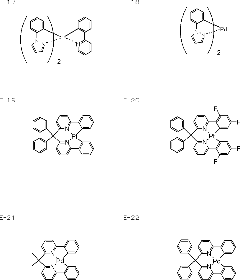
本発明の発光層に用いられる正孔輸送性ホスト材料としては、耐久性向上、駆動電圧低下の観点から、イオン化ポテンシャルIpが5.1eV以上6.4eV以下であることが好ましく、5.4eV以上6.2eV以下であることがより好ましく、5.6eV以上6.0eV以下であることが更に好ましい。また、耐久性向上、駆動電圧低下の観点から、電子親和力Eaが1.2eV以上3.1eV以下であることが好ましく、1.4eV以上3.0eV以下であることがより好ましく、1.8eV以上2.8eV以下であることが更に好ましい。
好ましい最低三重項励起準位(以下T1とする)は好ましくは2.2eV以上3.7eV以下であり、更に好ましくは2.4eV以上3.7eV以下であり、最も好ましくは2.4eV以上3.4eV以下である。 <Hole-transporting host material>
The hole transporting host material used in the light emitting layer of the present invention preferably has an ionization potential Ip of 5.1 eV or more and 6.4 eV or less from the viewpoint of improving durability and lowering driving voltage. It is more preferably 6.2 eV or less, and further preferably 5.6 eV or more and 6.0 eV or less. Further, from the viewpoint of improving durability and lowering driving voltage, the electron affinity Ea is preferably 1.2 eV or more and 3.1 eV or less, more preferably 1.4 eV or more and 3.0 eV or less, and 1.8 eV or more. More preferably, it is 2.8 eV or less.
A preferable lowest triplet excited level (hereinafter referred to as T1) is preferably 2.2 eV or more and 3.7 eV or less, more preferably 2.4 eV or more and 3.7 eV or less, and most preferably 2.4 eV or more and 3. 4 eV or less.
これらの中でも、インドール誘導体、カルバゾール誘導体、アザインドール誘導体、アザカルバゾール誘導体、芳香族第三級アミン化合物、チオフェン誘導体が好ましく、特に分子内にインドール骨格、カルバゾール骨格、アザインドール骨格、アザカルバゾール骨格、又は芳香族第三級アミン骨格を複数個有するものが好ましい。
また、本発明においてはホスト材料の水素を一部又はすべて重水素に置換したホスト材料を用いることができる(特願2008-126130号明細書、特表2004-515506号公報)。 Examples of the hole transporting host material include pyrrole, indole, carbazole, azaindole, azacarbazole, pyrazole, imidazole, polyarylalkane, pyrazoline, pyrazolone, phenylenediamine, arylamine, amino-substituted chalcone, styrylanthracene, and fluorenone. Hydrazone, stilbene, silazane, aromatic tertiary amine compound, styrylamine compound, aromatic dimethylidin compound, porphyrin compound, polysilane compound, poly (N-vinylcarbazole), aniline copolymer, thiophene oligomer, Examples thereof include conductive polymer oligomers such as polythiophene, organic silanes, carbon films, or derivatives thereof.
Among these, indole derivatives, carbazole derivatives, azaindole derivatives, azacarbazole derivatives, aromatic tertiary amine compounds, and thiophene derivatives are preferable, and indole skeleton, carbazole skeleton, azaindole skeleton, azacarbazole skeleton in the molecule, or Those having a plurality of aromatic tertiary amine skeletons are preferred.
In the present invention, a host material in which part or all of hydrogen in the host material is substituted with deuterium can be used (Japanese Patent Application No. 2008-126130, Japanese Patent Application Publication No. 2004-515506).
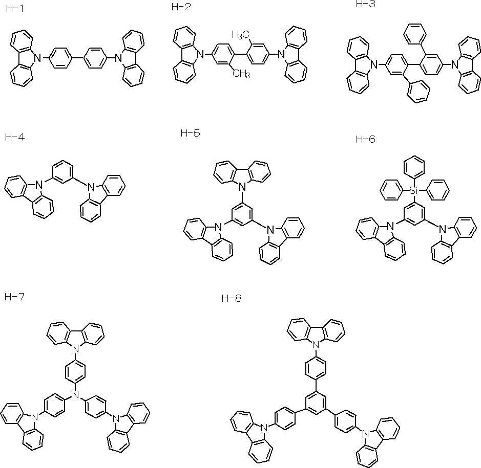


前記発光層は、特に制限はなく、公知の方法に従って形成することができるが、例えば、蒸着法、スパッタ法等の乾式製膜法、湿式塗布方式、転写法、印刷法、インクジェット方式、などにより好適に形成することができる。 The light-emitting layer receives holes from an anode, a hole injection layer, or a hole transport layer when an electric field is applied, receives electrons from a cathode, an electron injection layer, or an electron transport layer, and recombines holes and electrons. It is a layer having a function of providing a field to emit light.
The light emitting layer is not particularly limited and can be formed according to a known method. For example, by a dry film forming method such as a vapor deposition method or a sputtering method, a wet coating method, a transfer method, a printing method, an ink jet method, or the like. It can form suitably.
前記有機層は、少なくとも前記発光層を有し、電子輸送層、電子注入層、更に必要に応じて、正孔注入層、正孔輸送層、正孔ブロック層、電子ブロック層、などを有していてもよい。 The organic electroluminescent element of the present invention has an organic layer including a light emitting layer between an anode and a cathode, and may have other layers depending on the purpose.
The organic layer includes at least the light emitting layer, and includes an electron transport layer, an electron injection layer, and, if necessary, a hole injection layer, a hole transport layer, a hole block layer, an electron block layer, and the like. It may be.
前記電子注入層、電子輸送層は、陰極又は陰極側から電子を受け取り陽極側に輸送する機能を有する層である。
前記電子輸送層としては、前記電子輸送性ホスト材料、前記電子供与性ドーパント等の材料を含み形成される。 <Electron injection layer, electron transport layer>
The electron injection layer and the electron transport layer are layers having a function of receiving electrons from the cathode or the cathode side and transporting them to the anode side.
The electron transport layer includes a material such as the electron transport host material and the electron donating dopant.
前記電子輸送層の厚みとしては、1nm~500nmであるのが好ましく、5nm~200nmであるのがより好ましく、10nm~100nmであるのが更に好ましい。また、電子注入層の厚みとしては、0.1nm~200nmであるのが好ましく、0.2nm~100nmであるのがより好ましく、0.5nm~50nmであるのが更に好ましい。
前記電子注入層、電子輸送層は、1種又は2種以上の材料からなる単層構造であってもよいし、同一組成又は異種組成の複数層からなる多層構造であってもよい。 There is no restriction | limiting in particular as thickness of the said electron injection layer and an electron carrying layer, According to the objective, it can select suitably, From a viewpoint of reducing a drive voltage, it is preferable that it is each 500 nm or less.
The thickness of the electron transport layer is preferably 1 nm to 500 nm, more preferably 5 nm to 200 nm, and still more preferably 10 nm to 100 nm. The thickness of the electron injection layer is preferably 0.1 nm to 200 nm, more preferably 0.2 nm to 100 nm, and still more preferably 0.5 nm to 50 nm.
The electron injection layer and the electron transport layer may have a single layer structure made of one or more materials, or may have a multilayer structure made of a plurality of layers having the same composition or different compositions.
前記正孔注入層及び正孔輸送層は、陽極又は陽極側から正孔を受け取り陰極側に輸送する機能を有する層である。該正孔注入層及び正孔輸送層は、単層構造であってもよいし、同一組成又は異種組成の複数層からなる多層構造であってもよい。
これらの層に用いられる正孔注入材料、又は正孔輸送材料としては、低分子化合物であっても高分子化合物であってもよい。
前記正孔注入材料、又は正孔輸送材料としては、特に制限はなく、目的に応じて適宜選択することができ、例えばピロール誘導体、カルバゾール誘導体、トリアゾール誘導体、オキサゾール誘導体、オキサジアゾール誘導体、イミダゾール誘導体、ポリアリールアルカン誘導体、ピラゾリン誘導体、ピラゾロン誘導体、フェニレンジアミン誘導体、アリールアミン誘導体、アミノ置換カルコン誘導体、スチリルアントラセン誘導体、フルオレノン誘導体、ヒドラゾン誘導体、スチルベン誘導体、シラザン誘導体、芳香族第三級アミン化合物、スチリルアミン化合物、芳香族ジメチリディン系化合物、フタロシアニン系化合物、ポルフィリン系化合物、チオフェン誘導体、有機シラン誘導体、カーボン、などが挙げられる。これらは、1種単独で使用してもよいし、2種以上を併用してもよい。 <Hole injection layer, hole transport layer>
The hole injection layer and the hole transport layer are layers having a function of receiving holes from the anode or the anode side and transporting them to the cathode side. The hole injection layer and the hole transport layer may have a single layer structure or a multilayer structure composed of a plurality of layers having the same composition or different compositions.
The hole injection material or hole transport material used for these layers may be a low molecular compound or a high molecular compound.
The hole injection material or hole transport material is not particularly limited and may be appropriately selected depending on the intended purpose. Examples thereof include pyrrole derivatives, carbazole derivatives, triazole derivatives, oxazole derivatives, oxadiazole derivatives, imidazole derivatives. , Polyarylalkane derivatives, pyrazoline derivatives, pyrazolone derivatives, phenylenediamine derivatives, arylamine derivatives, amino-substituted chalcone derivatives, styrylanthracene derivatives, fluorenone derivatives, hydrazone derivatives, stilbene derivatives, silazane derivatives, aromatic tertiary amine compounds, styryl Examples include amine compounds, aromatic dimethylidin compounds, phthalocyanine compounds, porphyrin compounds, thiophene derivatives, organosilane derivatives, and carbon. These may be used individually by 1 type and may use 2 or more types together.
前記電子受容性ドーパントとしては、電子受容性で有機化合物を酸化する性質を有すれば、無機化合物でも有機化合物でも使用できる。
前記無機化合物としては、特に制限はなく、目的に応じて適宜選択することができ、例えば塩化第二鉄、塩化アルミニウム、塩化ガリウム、塩化インジウム、五塩化アンチモン等のハロゲン化金属;五酸化バナジウム、三酸化モリブデン等の金属酸化物、などが挙げられる。
前記有機化合物としては、特に制限はなく、目的に応じて適宜選択することができ、例えば置換基としてニトロ基、ハロゲン、シアノ基、トリフルオロメチル基等を有する化合物;キノン系化合物、酸無水物系化合物、フラーレン、などが挙げられる。
これらの電子受容性ドーパントは、1種単独で用いてもよいし、2種以上を用いてもよい。
前記電子受容性ドーパントの使用量は、材料の種類によって異なるが、正孔輸送層材料又は正孔注入材料に対して0.01質量%~50質量%が好ましく、0.05質量%~20質量%がより好ましく、0.1質量%~10質量%が更に好ましい。 The hole injection layer and the hole transport layer may contain an electron accepting dopant.
As the electron-accepting dopant, an inorganic compound or an organic compound can be used as long as it has an electron-accepting property and oxidizes an organic compound.
The inorganic compound is not particularly limited and may be appropriately selected depending on the intended purpose. Examples thereof include metal halides such as ferric chloride, aluminum chloride, gallium chloride, indium chloride and antimony pentachloride; vanadium pentoxide, And metal oxides such as molybdenum trioxide.
The organic compound is not particularly limited and may be appropriately selected depending on the intended purpose. For example, a compound having a nitro group, a halogen, a cyano group, a trifluoromethyl group or the like as a substituent; a quinone compound, an acid anhydride Compounds, fullerenes, and the like.
These electron-accepting dopants may be used alone or in combination of two or more.
The amount of the electron-accepting dopant used varies depending on the type of material, but is preferably 0.01% by mass to 50% by mass with respect to the hole transport layer material or the hole injection material, and 0.05% by mass to 20% by mass. % Is more preferable, and 0.1% by mass to 10% by mass is even more preferable.
前記正孔注入層及び正孔輸送層の厚さは、1nm~500nmが好ましく、5nm~200nmがより好ましく、10nm~100nmが更に好ましい。 The hole injection layer and the hole transport layer can be formed according to a known method, for example, a vapor deposition method, a dry film forming method such as a sputtering method, a wet coating method, a transfer method, a printing method, an ink jet method, It can form suitably by.
The thickness of the hole injection layer and the hole transport layer is preferably 1 nm to 500 nm, more preferably 5 nm to 200 nm, still more preferably 10 nm to 100 nm.
前記正孔ブロック層は、陽極側から発光層に輸送された正孔が陰極側に通り抜けることを防止する機能を有する層であり、通常、発光層と陰極側で隣接する有機化合物層として設けられる。
前記電子ブロック層は、陰極側から発光層に輸送された電子が陽極側に通り抜けることを防止する機能を有する層であり、通常、発光層と陽極側で隣接する有機化合物層として設けられる。
前記正孔ブロック層を構成する化合物の例としては、BAlq等のアルミニウム錯体、トリアゾール誘導体、BCP等のフェナントロリン誘導体、等が挙げられる。
前記電子ブロック層を構成する化合物の例としては、例えば前述の正孔輸送材料として挙げたものが利用できる。 <Hole blocking layer, electron blocking layer>
The hole blocking layer is a layer having a function of preventing holes transported from the anode side to the light emitting layer from passing through to the cathode side, and is usually provided as an organic compound layer adjacent to the light emitting layer on the cathode side. .
The electron blocking layer is a layer having a function of preventing electrons transported from the cathode side to the light emitting layer from passing through to the anode side, and is usually provided as an organic compound layer adjacent to the light emitting layer on the anode side.
Examples of the compound constituting the hole blocking layer include aluminum complexes such as BAlq, triazole derivatives, phenanthroline derivatives such as BCP, and the like.
As examples of the compound constituting the electron blocking layer, for example, those mentioned as the hole transporting material can be used.
前記正孔ブロック層及び電子ブロック層の厚さは、1nm~200nmであるのが好ましく、1nm~50nmであるのがより好ましく、3nm~10nmであるのが更に好ましい。また正孔ブロック層及び電子ブロック層は、上述した材料の1種又は2種以上からなる単層構造であってもよいし、同一組成又は異種組成の複数層からなる多層構造であってもよい。 The electron block layer and the hole block layer are not particularly limited and can be formed according to a known method, for example, a dry film forming method such as a vapor deposition method and a sputtering method, a wet coating method, a transfer method, and a printing method. It can be suitably formed by an inkjet method or the like.
The thickness of the hole blocking layer and the electron blocking layer is preferably 1 nm to 200 nm, more preferably 1 nm to 50 nm, and even more preferably 3 nm to 10 nm. In addition, the hole blocking layer and the electron blocking layer may have a single layer structure composed of one or more of the above-described materials, or may have a multilayer structure composed of a plurality of layers having the same composition or different compositions. .
本発明の有機電界発光素子は、一対の電極、即ち陽極と陰極とを含む。前記有機電界発光素子の性質上、陽極及び陰極のうち少なくとも一方の電極は透明であることが好ましい。通常、陽極は有機化合物層に正孔を供給する電極としての機能を有していればよく、陰極は有機化合物層に電子を注入する電極としての機能を有していればよい。
前記電極としては、その形状、構造、大きさ等については特に制限はなく、有機電界発光素子の用途、目的に応じて公知の電極材料の中から適宜選択することができる。
前記電極を構成する材料としては、例えば、金属、合金、金属酸化物、導電性化合物、又はこれらの混合物等が好適に挙げられる。 <Electrode>
The organic electroluminescent element of the present invention includes a pair of electrodes, that is, an anode and a cathode. In view of the nature of the organic electroluminescence device, at least one of the anode and the cathode is preferably transparent. Usually, the anode only needs to have a function as an electrode for supplying holes to the organic compound layer, and the cathode only needs to have a function as an electrode for injecting electrons into the organic compound layer.
The shape, structure, size and the like of the electrode are not particularly limited, and can be appropriately selected from known electrode materials according to the use and purpose of the organic electroluminescence device.
Suitable examples of the material constituting the electrode include metals, alloys, metal oxides, conductive compounds, and mixtures thereof.
前記陽極を構成する材料としては、例えば、アンチモンやフッ素等をドープした酸化錫(ATO、FTO)、酸化錫、酸化亜鉛、酸化インジウム、酸化インジウム錫(ITO)、酸化亜鉛インジウム(IZO)等の導電性金属酸化物;金、銀、クロム、ニッケル等の金属;これらの金属と導電性金属酸化物との混合物又は積層物;ヨウ化銅、硫化銅等の無機導電性物質;ポリアニリン、ポリチオフェン、ポリピロール等の有機導電性材料、又はこれらとITOとの積層物、などが挙げられる。これらの中でも、導電性金属酸化物が好ましく、生産性、高導電性、透明性等の点からはITOが特に好ましい。 -anode-
Examples of the material constituting the anode include tin oxide doped with antimony and fluorine (ATO, FTO), tin oxide, zinc oxide, indium oxide, indium tin oxide (ITO), and indium zinc oxide (IZO). Conductive metal oxides; metals such as gold, silver, chromium and nickel; mixtures or laminates of these metals and conductive metal oxides; inorganic conductive materials such as copper iodide and copper sulfide; polyaniline, polythiophene, Examples thereof include organic conductive materials such as polypyrrole, and laminates of these with ITO. Among these, a conductive metal oxide is preferable, and ITO is particularly preferable in terms of productivity, high conductivity, transparency, and the like.
前記陰極を構成する材料としては、例えば、アルカリ金属(例えばLi、Na、K、Cs等)、アルカリ土類金属(例えばMg、Ca等)、金、銀、鉛、アルミニウム、ナトリウム-カリウム合金、リチウム-アルミニウム合金、マグネシウム-銀合金、インジウム、イッテルビウム等の希土類金属、などが挙げられる。これらは、1種単独で使用してもよいが、安定性と電子注入性とを両立させる観点からは、2種以上を好適に併用することができる。
これらの中でも、電子注入性の点で、アルカリ金属やアルカリ土類金属が好ましく、保存安定性に優れる点で、アルミニウムを主体とする材料が好ましい。
前記アルミニウムを主体とする材料とは、アルミニウム単独、アルミニウムと0.01質量%~10質量%のアルカリ金属又はアルカリ土類金属との合金若しくはこれらの混合物(例えば、リチウム-アルミニウム合金、マグネシウム-アルミニウム合金など)をいう。 -cathode-
Examples of the material constituting the cathode include alkali metals (eg, Li, Na, K, Cs, etc.), alkaline earth metals (eg, Mg, Ca, etc.), gold, silver, lead, aluminum, sodium-potassium alloys, Examples thereof include lithium-aluminum alloys, magnesium-silver alloys, rare earth metals such as indium and ytterbium. These may be used alone, but two or more can be suitably used in combination from the viewpoint of achieving both stability and electron injection.
Among these, alkali metals and alkaline earth metals are preferable from the viewpoint of electron injecting property, and materials mainly composed of aluminum are preferable from the viewpoint of excellent storage stability.
The material mainly composed of aluminum is aluminum alone, an alloy of aluminum and 0.01% by mass to 10% by mass of alkali metal or alkaline earth metal, or a mixture thereof (for example, lithium-aluminum alloy, magnesium-aluminum). Alloy).
本発明の有機電界発光素子は、基板上に設けられていることが好ましく、電極と基板とが直接接する形で設けられていてもよいし、中間層を介在する形で設けられていてもよい。
前記基板の材料としては、特に制限はなく、目的に応じて適宜選択することができ、例えばイットリア安定化ジルコニア(YSZ)、ガラス(無アルカリガラス、ソーダライムガラス等)等の無機材料;ポリエチレンテレフタレート、ポリブチレンフタレート、ポリエチレンナフタレート等のポリエステル;ポリスチレン、ポリカーボネート、ポリエーテルスルホン、ポリアリレート、ポリイミド、ポリシクロオレフィン、ノルボルネン樹脂、ポリ(クロロトリフルオロエチレン)等の有機材料、などが挙げられる。 <Board>
The organic electroluminescent element of the present invention is preferably provided on a substrate, and may be provided in such a manner that the electrode and the substrate are in direct contact with each other, or may be provided with an intermediate layer interposed. .
The material for the substrate is not particularly limited and may be appropriately selected depending on the intended purpose. Examples thereof include inorganic materials such as yttria-stabilized zirconia (YSZ) and glass (such as alkali-free glass and soda lime glass); polyethylene terephthalate And polyesters such as polybutylene phthalate and polyethylene naphthalate; organic materials such as polystyrene, polycarbonate, polyethersulfone, polyarylate, polyimide, polycycloolefin, norbornene resin, and poly (chlorotrifluoroethylene).
前記透湿防止層(ガスバリア層)の材料としては、例えば窒化珪素、酸化珪素等の無機物などが挙げられる。
前記透湿防止層(ガスバリア層)は、例えば高周波スパッタリング法などにより形成することができる。 The substrate may be provided with a moisture permeation preventing layer (gas barrier layer) on the front surface or the back surface.
Examples of the material of the moisture permeation preventive layer (gas barrier layer) include inorganic substances such as silicon nitride and silicon oxide.
The moisture permeation preventing layer (gas barrier layer) can be formed by, for example, a high frequency sputtering method.
有機電界発光素子全体は、保護層によって保護されていてもよい。
前記保護層に含まれる材料としては、水分や酸素等の素子劣化を促進するものが素子内に入ることを抑止する機能を有しているものであれば特に制限はなく、目的に応じて適宜選択することができ、例えばIn、Sn、Pb、Au、Cu、Ag、Al、Ti、Ni等の金属;MgO、SiO、SiO2、Al2O3、GeO、NiO、CaO、BaO、Fe2O3、Y2O3、TiO2等の金属酸化物;SiNx、SiNxOy等の金属窒化物;MgF2、LiF、AlF3、CaF2等の金属フッ化物;ポリエチレン、ポリプロピレン、ポリメチルメタクリレート、ポリイミド、ポリウレア、ポリテトラフルオロエチレン、ポリクロロトリフルオロエチレン、ポリジクロロジフルオロエチレン、クロロトリフルオロエチレンとジクロロジフルオロエチレンとの共重合体、テトラフルオロエチレンと少なくとも1種のコモノマーとを含むモノマー混合物を共重合させて得られる共重合体、共重合主鎖に環状構造を有する含フッ素共重合体、吸水率1%以上の吸水性物質、吸水率0.1%以下の防湿性物質、などが挙げられる。 -Protective layer-
The entire organic electroluminescent element may be protected by a protective layer.
The material contained in the protective layer is not particularly limited as long as it has a function of suppressing the entry of elements that promote element deterioration such as moisture and oxygen into the element. For example, metals such as In, Sn, Pb, Au, Cu, Ag, Al, Ti, Ni; MgO, SiO, SiO 2 , Al 2 O 3 , GeO, NiO, CaO, BaO, Fe 2 Metal oxides such as O 3 , Y 2 O 3 and TiO 2 ; Metal nitrides such as SiNx and SiNxOy; Metal fluorides such as MgF 2 , LiF, AlF 3 and CaF 2 ; Polyethylene, polypropylene, polymethyl methacrylate, polyimide , Polyurea, polytetrafluoroethylene, polychlorotrifluoroethylene, polydichlorodifluoroethylene, chlorotrifluoroethylene A copolymer of dichlorodifluoroethylene, a copolymer obtained by copolymerizing a monomer mixture containing tetrafluoroethylene and at least one comonomer, a fluorinated copolymer having a cyclic structure in the copolymer main chain, water absorption Examples thereof include a water-absorbing substance having a rate of 1% or more, a moisture-proof substance having a water absorption rate of 0.1% or less, and the like.
本発明の有機電界発光素子は、封止容器を用いて素子全体が封止されていてもよい。更に、前記封止容器と有機電界発光素子の間の空間には、水分吸収剤又は不活性液体を封入してもよい。
前記水分吸収剤としては、特に制限はなく、目的に応じて適宜選択することができ、例えば酸化バリウム、酸化ナトリウム、酸化カリウム、酸化カルシウム、硫酸ナトリウム、硫酸カルシウム、硫酸マグネシウム、五酸化燐、塩化カルシウム、塩化マグネシウム、塩化銅、フッ化セシウム、フッ化ニオブ、臭化カルシウム、臭化バナジウム、モレキュラーシーブ、ゼオライト、酸化マグネシウム、などが挙げられる。
前記不活性液体としては、特に制限はなく、目的に応じて適宜選択することができ、例えばパラフィン類、流動パラフィン類;パーフルオロアルカン、パーフルオロアミン、パーフルオロエーテル等のフッ素系溶剤;塩素系溶剤、シリコーンオイル類、などが挙げられる。 -Sealing container-
As for the organic electroluminescent element of this invention, the whole element may be sealed using the sealing container. Furthermore, a water absorbent or an inert liquid may be sealed in the space between the sealing container and the organic electroluminescent element.
The moisture absorbent is not particularly limited and may be appropriately selected depending on the intended purpose. For example, barium oxide, sodium oxide, potassium oxide, calcium oxide, sodium sulfate, calcium sulfate, magnesium sulfate, phosphorus pentoxide, chloride Calcium, magnesium chloride, copper chloride, cesium fluoride, niobium fluoride, calcium bromide, vanadium bromide, molecular sieve, zeolite, magnesium oxide, and the like can be given.
The inert liquid is not particularly limited and may be appropriately selected depending on the intended purpose. Examples thereof include paraffins, liquid paraffins; fluorinated solvents such as perfluoroalkane, perfluoroamine, and perfluoroether; Examples include solvents and silicone oils.
本発明の有機電界発光素子は、大気からの酸素や水分による素子性能劣化を樹脂封止層により封止することで抑制することが好ましい。
前記樹脂封止層の樹脂素材としては、特に制限はなく、目的に応じて適宜選択することができ、例えばアクリル樹脂、エポキシ樹脂、フッ素系樹脂、シリコーン系樹脂、ゴム系樹脂、エステル系樹脂、などが挙げられる。これらの中でも、水分防止機能の点からエポキシ樹脂が特に好ましい。前記エポキシ樹脂の中でも熱硬化型エポキシ樹脂、又は光硬化型エポキシ樹脂が好ましい。 -Resin sealing layer-
The organic electroluminescent element of the present invention is preferably suppressed by sealing the element performance deterioration due to oxygen and moisture from the atmosphere with a resin sealing layer.
The resin material for the resin sealing layer is not particularly limited and can be appropriately selected depending on the purpose. For example, acrylic resin, epoxy resin, fluorine resin, silicone resin, rubber resin, ester resin, Etc. Among these, an epoxy resin is particularly preferable from the viewpoint of moisture prevention function. Among the epoxy resins, a thermosetting epoxy resin or a photocurable epoxy resin is preferable.
本発明に用いられる封止接着剤は、端部よりの水分や酸素の侵入を防止する機能を有する。
前記封止接着剤の材料としては、前記樹脂封止層で用いる材料と同じものを用いることができる。これらの中でも、水分防止の点からエポキシ系の接着剤が好ましく、光硬化型接着剤あるいは熱硬化型接着剤が特に好ましい。
前記封止接着剤にフィラーを添加することも好ましい。前記フィラーとしては、例えばSiO2、SiO(酸化ケイ素)、SiON(酸窒化ケイ素)、SiN(窒化ケイ素)等の無機材料が好ましい。該フィラーの添加により、封止接着剤の粘度が上昇し、加工適正が向上し、及び耐湿性が向上する。
前記封止接着剤は、乾燥剤を含有してもよい。前記乾燥剤としては、例えば酸化バリウム、酸化カルシウム、酸化ストロンチウム、などが挙げられる。前記乾燥剤の添加量は、前記封止接着剤に対し0.01質量%~20質量%が好ましく、0.05質量%~15質量%がより好ましい。前記添加量が、0.01質量%未満であると、乾燥剤の添加効果が薄れることになり、20質量%を超えると、封止接着剤中に乾燥剤を均一分散させることが困難になることがある。
本発明においては、前記乾燥剤の入った封止接着剤をディスペンサー等により任意量塗布し、塗布後第2基板を重ねて、硬化させることにより封止することができる。 -Sealing adhesive-
The sealing adhesive used in the present invention has a function of preventing intrusion of moisture and oxygen from the end portion.
As the material of the sealing adhesive, the same material as that used for the resin sealing layer can be used. Among these, an epoxy adhesive is preferable from the viewpoint of moisture prevention, and a photocurable adhesive or a thermosetting adhesive is particularly preferable.
It is also preferable to add a filler to the sealing adhesive. As the filler, for example SiO 2, SiO (silicon oxide), SiON (silicon oxynitride), an inorganic material such as SiN (silicon nitride) are preferred. Addition of the filler increases the viscosity of the sealing adhesive, improves processing suitability, and improves moisture resistance.
The sealing adhesive may contain a desiccant. Examples of the desiccant include barium oxide, calcium oxide, and strontium oxide. The addition amount of the desiccant is preferably 0.01% by mass to 20% by mass and more preferably 0.05% by mass to 15% by mass with respect to the sealing adhesive. When the addition amount is less than 0.01% by mass, the effect of adding the desiccant is diminished, and when it exceeds 20% by mass, it is difficult to uniformly disperse the desiccant in the sealing adhesive. Sometimes.
In this invention, it can seal by apply | coating arbitrary amounts of the sealing adhesive containing the said desiccant with a dispenser etc., and pile | stacking and hardening a 2nd board | substrate after application | coating.
本発明の有機電界発光素子は、陽極と陰極との間に直流(必要に応じて交流成分を含んでもよい)電圧(通常2ボルト~15ボルト)、又は直流電流を印加することにより、発光を得ることができる。
本発明の有機電界発光素子は、薄膜トランジスタ(TFT)によりアクティブマトリックスへ適用することができる。薄膜トランジスタの活性層としてアモルファスシリコン、高温ポリシリコン、低温ポリシリコン、微結晶シリコン、酸化物半導体、有機半導体、カーボンナノチューブ等を適用することができる。
本発明の有機電界発光素子は、例えばWO2005/088726号パンフレット、特開2006-165529号公報、米国特許出願公開2008/0237598A1明細書などに記載の薄膜トランジスタを適用することができる。 -Drive-
The organic electroluminescence device of the present invention emits light by applying a direct current (which may include an alternating current component as necessary) voltage (usually 2 to 15 volts) or a direct current between the anode and the cathode. Obtainable.
The organic electroluminescent element of the present invention can be applied to an active matrix by a thin film transistor (TFT). As the active layer of the thin film transistor, amorphous silicon, high temperature polysilicon, low temperature polysilicon, microcrystalline silicon, oxide semiconductor, organic semiconductor, carbon nanotube, or the like can be used.
For example, the thin film transistors described in WO2005 / 088826, JP-A-2006-165529, US Patent Application Publication No. 2008 / 0237598A1, and the like can be applied to the organic electroluminescent device of the present invention.
本発明の有機電界発光素子からの光取り出し方式は、トップエミッション方式であってもボトムエミッション方式であってもよい。 There is no restriction | limiting in particular in the organic electroluminescent element of this invention, Light extraction efficiency can be improved with various well-known devices. For example, by processing the substrate surface shape (for example, forming a fine uneven pattern), controlling the refractive index of the substrate, ITO layer, organic layer, controlling the film thickness of the substrate, ITO layer, organic layer, etc. It is possible to improve light extraction efficiency and external quantum efficiency.
The light extraction method from the organic electroluminescence device of the present invention may be a top emission method or a bottom emission method.
別の好ましい態様では、透明基板上に、透明又は半透明電極と金属電極がそれぞれ反射板として機能して、発光層で生じた光はその間で反射を繰り返し共振する。
共振構造を形成するためには、2つの反射板の有効屈折率、反射板間の各層の屈折率と厚みから決定される光路長を所望の共振波長の得るのに最適な値となるよう調整される。第一の態様の場合の計算式は、特開平9-180883号公報に記載されている。第2の態様の場合の計算式は、特開2004-127795号公報に記載されている。 The organic electroluminescent element of the present invention may have a resonator structure. For example, a multilayer mirror made of a plurality of laminated films having different refractive indexes, a transparent or translucent electrode, a light emitting layer, and a metal electrode are superimposed on a transparent substrate. The light generated in the light emitting layer resonates repeatedly with the multilayer mirror and the metal electrode as a reflection plate.
In another preferred embodiment, a transparent or translucent electrode and a metal electrode each function as a reflecting plate on a transparent substrate, and light generated in the light emitting layer repeats reflection and resonates between them.
In order to form a resonant structure, the optical path length determined from the effective refractive index of the two reflectors and the refractive index and thickness of each layer between the reflectors is adjusted to the optimum value to obtain the desired resonant wavelength. Is done. The calculation formula in the case of the first embodiment is described in JP-A-9-180883. The calculation formula in the case of the second aspect is described in JP-A No. 2004-127795.
本発明の有機電界発光素子は、特に制限はなく、目的に応じて適宜選択することができるが、表示素子、ディスプレイ、バックライト、電子写真、照明光源、記録光源、露光光源、読み取り光源、標識、看板、インテリア、光通信等に好適に利用できる。
前記有機ELディスプレイをフルカラータイプのものとする方法としては、例えば「月刊ディスプレイ」、2000年9月号、33~37ページに記載されているように、色の3原色(青色(B)、緑色(G)、赤色(R))に対応する光をそれぞれ発光する有機EL素子を基板上に配置する3色発光法、白色発光用の有機電界発光素子による白色発光をカラーフィルターを通して3原色に分ける白色法、青色発光用の有機電界発光素子による青色発光を蛍光色素層を通して赤色(R)及び緑色(G)に変換する色変換法、などが知られている。また、上記方法により得られる異なる発光色の有機電界発光素子を複数組み合わせて用いることにより、所望の発光色の平面型光源を得ることができる。例えば、青色及び黄色の発光素子を組み合わせた白色発光光源、青色、緑色、赤色の発光素子を組み合わせた白色発光光源、などが挙げられる。 -Applications-
The organic electroluminescent element of the present invention is not particularly limited and may be appropriately selected depending on the intended purpose. However, the display element, display, backlight, electrophotography, illumination light source, recording light source, exposure light source, reading light source, label It can be suitably used for signboards, interiors, optical communications, and the like.
As a method for making the organic EL display a full color type, as described in, for example, “Monthly Display”, September 2000, pages 33-37, the three primary colors (blue (B), green (G), red light (R)), a three-color light emitting method in which organic EL elements that emit light corresponding to red (R) are arranged on a substrate, and white light emission by an organic electroluminescent element for white light emission is divided into three primary colors through a color filter. A white method, a color conversion method for converting blue light emitted by an organic electroluminescent element for blue light emission into red (R) and green (G) through a fluorescent dye layer, and the like are known. Moreover, the planar light source of desired luminescent color can be obtained by using combining the organic electroluminescent element of the different luminescent color obtained by the said method. For example, a white light-emitting light source combining blue and yellow light-emitting elements, a white light-emitting light source combining blue, green, and red light-emitting elements can be used.
-有機電界発光素子の作製-
0.5mm厚み、2.5cm角のガラス基板を洗浄容器に入れ、2-プロパノール中で超音波洗浄した後、30分間UV-オゾン処理を行った。このガラス基板上に真空蒸着法にて以下の各層を蒸着した。なお、以下の実施例及び比較例における蒸着速度は、特に断りのない場合は0.2nm/秒である。蒸着速度は水晶振動子を用いて測定した。また、以下の各層厚は水晶振動子を用いて測定した。 (Comparative Example 1)
-Fabrication of organic electroluminescence device-
A glass substrate having a thickness of 0.5 mm and a square of 2.5 cm was placed in a cleaning container, subjected to ultrasonic cleaning in 2-propanol, and then subjected to UV-ozone treatment for 30 minutes. The following layers were deposited on this glass substrate by vacuum deposition. In addition, the vapor deposition rate in the following examples and comparative examples is 0.2 nm / second unless otherwise specified. The deposition rate was measured using a quartz resonator. The following layer thicknesses were measured using a crystal resonator.
次に、陽極(ITO)上に、正孔注入層として2-TNATA(4,4’,4”-Tris(N-(2-naphtyl)-N-phenyl-amino)-triphenylamine)を厚み140nmに蒸着した。
次に、正孔注入層上に、正孔輸送層としてα-NPD(Bis[N-(1-naphthyl)-N-pheny]benzidine)を厚み7nmに蒸着した。
次に、正孔輸送層上に、第二の正孔輸送層として下記構造式で表されるアミン化合物1を厚み3nmに蒸着した。

Next, on the anode (ITO), 2-TNATA (4,4 ′, 4 ″ -Tris (N- (2-naphthyl) -N-phenyl-amino) -triphenylamine) is formed to a thickness of 140 nm as a hole injection layer. Evaporated.
Next, α-NPD (Bis [N- (1-naphthyl) -N-pheny] benzidine) was deposited as a hole transport layer on the hole injection layer to a thickness of 7 nm.
Next, on the hole transport layer, an amine compound 1 represented by the following structural formula was deposited as a second hole transport layer to a thickness of 3 nm.


次に、電子輸送層上に、電子注入層としてLiFを厚み1nmとなるように蒸着した。
次に、電子注入層上に、陰極としてパタ-ニングしたマスク(発光領域が2mm×2mmとなるマスク)を設置し、金属アルミニウムを厚み100nmとなるように蒸着した。
以上により作製した積層体を、アルゴンガスで置換したグローブボックス内に入れ、ステンレス製の封止缶、及び紫外線硬化型の接着剤(XNR5516HV、長瀬チバ株式会社製)を用いて封止した。以上により、比較例1の有機電界発光素子を作製した。 Next, a nitrogen-containing heterocyclic derivative 1 represented by the following structural formula, which is a highly electron-transporting material contained in the general formula (1) as an electron transporting layer, was deposited to a thickness of 40 nm on the light emitting layer.
Next, LiF was deposited as an electron injection layer on the electron transport layer so as to have a thickness of 1 nm.
Next, a mask patterned as a cathode (a mask having a light emitting area of 2 mm × 2 mm) was placed on the electron injection layer, and metal aluminum was deposited to a thickness of 100 nm.
The laminate produced as described above was put in a glove box substituted with argon gas, and sealed with a stainless steel sealing can and an ultraviolet curable adhesive (XNR5516HV, manufactured by Nagase Ciba Co., Ltd.). Thus, an organic electroluminescent element of Comparative Example 1 was produced.
-有機電界発光素子の作製-
比較例1において、電子輸送層として低電子輸送性材料であるBAlq〔Bis-(2-methyl-8-quinolinolato)-4-(phenyl-phenolate)-aluminium-(III)〕を用いた以外は、比較例1と同様にして、有機電界発光素子を作製した。 (Comparative Example 2)
-Fabrication of organic electroluminescence device-
In Comparative Example 1, except that BAlq [Bis- (2-methyl-8-quinolinolato) -4- (phenyl-phenolate) -aluminum- (III)], which is a low electron transport material, was used as the electron transport layer. In the same manner as in Comparative Example 1, an organic electroluminescent element was produced.
-有機電界発光素子の作製-
比較例2において、発光材料として一般式(2)に含まれる電子輸送性燐光発光材料である下記構造式で表されるD-1を用いた以外は、比較例2と同様にして、有機電界発光素子を作製した。

-Fabrication of organic electroluminescence device-
In Comparative Example 2, an organic electric field was obtained in the same manner as in Comparative Example 2, except that D-1 represented by the following structural formula, which is an electron transporting phosphorescent light emitting material included in the general formula (2), was used as the light emitting material. A light emitting element was manufactured.
-有機電界発光素子の作製-
比較例1において、発光材料としてFirpicの代わりに上記構造式で表されるD-1を用いた以外は、比較例1と同様にして、有機電界発光素子を作製した。 Example 1
-Fabrication of organic electroluminescence device-
In Comparative Example 1, an organic electroluminescent element was produced in the same manner as Comparative Example 1 except that D-1 represented by the above structural formula was used as the light emitting material instead of Ferric.
-有機電界発光素子の作製-
実施例1において、電子輸送層として下記構造式で表される含窒素複素環誘導体2を用いた以外は、実施例1と同様にして、有機電界発光素子を作製した。

-Fabrication of organic electroluminescence device-
In Example 1, an organic electroluminescent element was produced in the same manner as in Example 1 except that the nitrogen-containing
-有機電界発光素子の作製-
実施例1において、電子輸送層として下記構造式で表される含窒素複素環誘導体3を用いた以外は、実施例1と同様にして、有機電界発光素子を作製した。

-Fabrication of organic electroluminescence device-
In Example 1, an organic electroluminescent element was produced in the same manner as in Example 1 except that the nitrogen-containing
-有機電界発光素子の作製-
実施例1において、電子輸送層として下記構造式で表される含窒素複素環誘導体4を用いた以外は、実施例1と同様にして、有機電界発光素子を作製した。

-Fabrication of organic electroluminescence device-
In Example 1, an organic electroluminescent element was produced in the same manner as in Example 1 except that the nitrogen-containing
-有機電界発光素子の作製-
実施例1において、発光材料として下記構造式で表されるD-2を用いた以外は、実施例1と同様にして、有機電界発光素子を作製した。
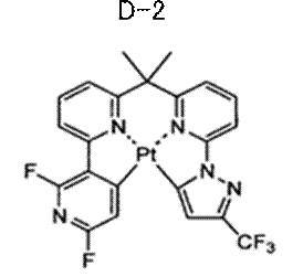
-Fabrication of organic electroluminescence device-
An organic electroluminescent element was produced in the same manner as in Example 1 except that D-2 represented by the following structural formula was used as the light emitting material in Example 1.
-有機電界発光素子の作製-
実施例5において、ホスト材料として下記構造式で表されるH-24を用い、電子輸送層として上記構造式で表される含窒素複素環誘導体2を用いた以外は、実施例5と同様にして、有機電界発光素子を作製した。

-Fabrication of organic electroluminescence device-
In Example 5, H-24 represented by the following structural formula was used as the host material, and the nitrogen-containing
-有機電界発光素子の作製-
実施例5において、ホスト材料として下記構造式で表されるH-27を用い、電子輸送層として上記構造式で表される含窒素複素環誘導体3を用いた以外は、実施例5と同様にして、有機電界発光素子を作製した。

-Fabrication of organic electroluminescence device-
In Example 5, H-27 represented by the following structural formula was used as the host material, and the nitrogen-containing
-有機電界発光素子の作製-
実施例1において、ホスト材料として下記構造式で表されるH-17を用い、発光材料として下記構造式で表されるD-3を用い、電子輸送層として上記構造式で表される含窒素複素環誘導体4を用いた以外は、実施例1と同様にして、有機電界発光素子を作製した。


-Fabrication of organic electroluminescence device-
In Example 1, H-17 represented by the following structural formula was used as the host material, D-3 represented by the following structural formula was used as the light emitting material, and the nitrogen-containing compound represented by the above structural formula was used as the electron transport layer. An organic electroluminescent element was produced in the same manner as in Example 1 except that the
-有機電界発光素子の作製-
実施例1において、発光材料として下記構造式で表されるD-4を用いた以外は、実施例1と同様にして、有機電界発光素子を作製した。
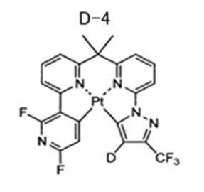
-Fabrication of organic electroluminescence device-
In Example 1, an organic electroluminescent element was produced in the same manner as in Example 1 except that D-4 represented by the following structural formula was used as the luminescent material.
-有機電界発光素子の作製-
実施例9において、ホスト材料として上記構造式で表されるH-24を用い、電子輸送層として上記構造式で表される含窒素複素環誘導体2を用いた以外は、実施例9と同様にして、有機電界発光素子を作製した。 (Example 10)
-Fabrication of organic electroluminescence device-
In Example 9, H-24 represented by the above structural formula was used as the host material, and the nitrogen-containing
-有機電界発光素子の作製-
実施例1において、発光材料として下記構造式で表されるD-5を用い、電子輸送層として上記構造式で表される含窒素複素環誘導体3を用いた以外は、実施例1と同様にして、有機電界発光素子を作製した。

-Fabrication of organic electroluminescence device-
In Example 1, D-5 represented by the following structural formula was used as the luminescent material, and a nitrogen-containing
-有機電界発光素子の作製-
実施例1において、発光材料として下記構造式で表されるD-9を用い、電子輸送層として上記構造式で表される含窒素複素環誘導体4を用いた以外は、実施例1と同様にして、有機電界発光素子を作製した。

-Fabrication of organic electroluminescence device-
In Example 1, D-9 represented by the following structural formula was used as the light emitting material, and the nitrogen-containing
-有機電界発光素子の作製-
実施例12において、電子輸送層として上記構造式で表される含窒素複素環誘導体1を用いた以外は、実施例12と同様にして、有機電界発光素子を作製した。 (Example 13)
-Fabrication of organic electroluminescence device-
In Example 12, an organic electroluminescent element was produced in the same manner as in Example 12 except that the nitrogen-containing heterocyclic derivative 1 represented by the above structural formula was used as the electron transport layer.
-有機電界発光素子の作製-
実施例2において、発光材料として下記構造式で表されるD-10を用いた以外は、実施例2と同様にして、有機電界発光素子を作製した。

-Fabrication of organic electroluminescence device-
In Example 2, an organic electroluminescent element was produced in the same manner as in Example 2 except that D-10 represented by the following structural formula was used as the light emitting material.
-有機電界発光素子の作製-
実施例14において、電子輸送層として上記構造式で表される含窒素複素環誘導体3を用いた以外は、実施例14と同様にして、有機電界発光素子を作製した。 (Example 15)
-Fabrication of organic electroluminescence device-
In Example 14, an organic electroluminescent element was produced in the same manner as in Example 14 except that the nitrogen-containing
-有機電界発光素子の作製-
実施例4において、発光材料として下記構造式で表されるD-14を用いた以外は、実施例4と同様にして、有機電界発光素子を作製した。

-Fabrication of organic electroluminescence device-
In Example 4, an organic electroluminescent device was produced in the same manner as in Example 4 except that D-14 represented by the following structural formula was used as the luminescent material.
-有機電界発光素子の作製-
実施例1において、発光材料として下記構造式で表されるD-15を用いた以外は、実施例1と同様にして、有機電界発光素子を作製した。

-Fabrication of organic electroluminescence device-
An organic electroluminescent element was produced in the same manner as in Example 1 except that D-15 represented by the following structural formula was used as the light emitting material in Example 1.
-有機電界発光素子の作製-
実施例2において、発光材料として下記構造式で表されるD-23を用いた以外は、実施例2と同様にして、有機電界発光素子を作製した。

-Fabrication of organic electroluminescence device-
In Example 2, an organic electroluminescent element was produced in the same manner as in Example 2 except that D-23 represented by the following structural formula was used as the light emitting material.
-有機電界発光素子の作製-
実施例3において、発光材料として下記構造式で表されるD-24を用いた以外は、実施例3と同様にして、有機電界発光素子を作製した。

-Fabrication of organic electroluminescence device-
In Example 3, an organic electroluminescent element was produced in the same manner as in Example 3 except that D-24 represented by the following structural formula was used as the light emitting material.
-有機電界発光素子の作製-
実施例19において、電子輸送層として上記構造式で表される含窒素複素環誘導体4を用いた以外は、実施例19と同様にして、有機電界発光素子を作製した。 (Example 20)
-Fabrication of organic electroluminescence device-
In Example 19, an organic electroluminescent element was produced in the same manner as in Example 19 except that the nitrogen-containing
東陽テクニカ株式会社製ソースメジャーユニット2400を用いて、直流電圧を各素子に印加し、発光させた。電流が10mA/cm2となったときの電圧を駆動電圧として測定した。 <Measurement of drive voltage>
Using a source measure unit 2400 manufactured by Toyo Technica Co., Ltd., a DC voltage was applied to each element to emit light. The voltage when the current reached 10 mA / cm 2 was measured as the driving voltage.
東陽テクニカ株式会社製ソースメジャーユニット2400を用いて、直流電圧を各素子に印加し、発光させた。発光スペクトル・輝度はトプコン社製スペクトルアナライザーSR-3を用いて測定し、これらの数値をもとに電流が10mA/cm2における外部量子効率を輝度換算法により算出した。 <Measurement of external quantum efficiency>
Using a source measure unit 2400 manufactured by Toyo Technica Co., Ltd., a DC voltage was applied to each element to emit light. The emission spectrum and luminance were measured using a spectrum analyzer SR-3 manufactured by Topcon Corporation, and the external quantum efficiency at a current of 10 mA / cm 2 was calculated by the luminance conversion method based on these numerical values.

表1の結果から、比較例1と比較例2を比較した場合、正孔輸送性燐光発光材料であるFirpicを用いた場合は、電子輸送層を低電子輸送性材料であるBAlqから高電子輸送性材料である含窒素複素環誘導体1に変えたところ、確かに駆動電圧は低下しているが、外部量子効率の低下が生じてしまい、せっかくの燐光発光による高い量子効率と低電圧化を両立させることができなかった。
しかし、電子輸送性燐光発光材料率のである四座配位子白金錯体(D-1)を用いた比較例3と実施例1を比較すると、電子輸送層をBAlqから含窒素複素環誘導体1に変えることにより、大幅な低電圧化が見られ、更に外部量子効率は高い効率を維持させることができた。また、実施例2~4では一般式(1)を満たす含窒素複素環誘導体3種類で同様の効果が認められ、実施例5~20では一般式(2)を満たす電子輸送性燐光発光材料においてやはり同様の効果が認められた。
From the results shown in Table 1, when Comparative Example 1 and Comparative Example 2 are compared, when Firpic, which is a hole transporting phosphorescent material, is used, the electron transport layer is transferred from BAlq, which is a low electron transport material, to high electron transport. When the nitrogen-containing heterocyclic derivative 1, which is a functional material, is changed, the driving voltage is certainly lowered, but the external quantum efficiency is lowered, and both high quantum efficiency and low voltage due to the phosphorescence emission are achieved. I couldn't let you.
However, comparing Comparative Example 3 and Example 1 using a tetradentate platinum complex (D-1) having an electron transporting phosphorescent material ratio, the electron transporting layer is changed from BAlq to nitrogen-containing heterocyclic derivative 1. As a result, a significant reduction in voltage was observed, and the external quantum efficiency could be maintained at a high level. In Examples 2 to 4, similar effects were observed with three types of nitrogen-containing heterocyclic derivatives satisfying the general formula (1). In Examples 5 to 20, the electron-transporting phosphorescent light-emitting material satisfying the general formula (2) was used. The same effect was recognized.
-有機電界発光素子の作製-
比較例1において、正孔注入層の2-TNATAを、DNTPD(N,N’-bis-[4-(di-m-tolylamino)phenyl]-N,N’-diphenylbiphenyl-4,4’-diamine)に代えた以外は、比較例1と同様にして、有機電界発光素子を作製した。 (Comparative Example 4)
-Fabrication of organic electroluminescence device-
In Comparative Example 1, 2-TNATA of the hole injection layer was changed to DNTPD (N, N′-bis- [4- (di-m-tolylamino) phenyl] -N, N′-diphenylbiphenyl-4,4′-diamine). An organic electroluminescent element was produced in the same manner as in Comparative Example 1 except that the above was replaced.
-有機電界発光素子の作製-
比較例4において、発光材料としてFirpicを下記構造式で表されるD-1に代えた以外は、比較例4と同様にして、有機電界発光素子を作製した。
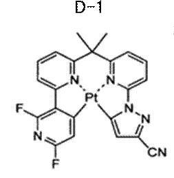
-Fabrication of organic electroluminescence device-
An organic electroluminescent element was produced in the same manner as in Comparative Example 4 except that, in Comparative Example 4, Firepic was changed to D-1 represented by the following structural formula as the light emitting material.
-有機電界発光素子の作製-
実施例21において、電子輸送層として下記構造式で表される含窒素複素環誘導体2を用いた以外は、実施例21と同様にして、有機電界発光素子を作製した。
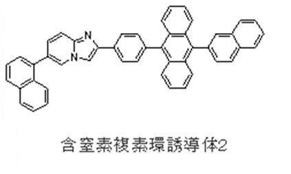
-Fabrication of organic electroluminescence device-
In Example 21, an organic electroluminescent element was produced in the same manner as in Example 21 except that the nitrogen-containing
-有機電界発光素子の作製-
実施例21において、電子輸送層として下記構造式で表される含窒素複素環誘導体3を用いた以外は、実施例21と同様にして、有機電界発光素子を作製した。

-Fabrication of organic electroluminescence device-
In Example 21, an organic electroluminescent element was produced in the same manner as in Example 21 except that the nitrogen-containing

Claims (12)
- 陽極と陰極の間に、発光層を含む少なくとも一層の有機層を有してなり、
前記有機層における少なくとも1層が、下記一般式(1)で表される含窒素複素環誘導体から選択される少なくとも1種を含有し、かつ前記有機層における少なくとも1層が、下記一般式(2)で表される電子輸送性燐光発光材料を含有することを特徴とする有機電界発光素子。

ただし、前記一般式(1)中、A1~A3は、それぞれ独立に、窒素原子又は炭素原子である。Ar1は、置換もしくは無置換の核炭素数6~60のアリール基、又は置換もしくは無置換の核炭素数3~60のヘテロアリール基である。Ar2は、水素原子、置換もしくは無置換の核炭素数6~60のアリール基、置換もしくは無置換の核炭素数3~60のヘテロアリール基、置換もしくは無置換の炭素数1~20のアルキル基、又は置換もしくは無置換の炭素数1~20のアルコキシ基である。ただし、Ar1及びAr2のいずれか一方は、置換もしくは無置換の核炭素数10~60の縮合環基、又は置換もしくは無置換の核炭素数3~60のモノヘテロ縮合環基である。L1及びL2は、それぞれ独立に、単結合、置換もしくは無置換の核炭素数6~60のアリーレン基、置換もしくは無置換の核炭素数3~60のヘテロアリーレン基、又は置換もしくは無置換のフルオレニレン基である。Rは、水素原子、置換もしくは無置換の核炭素数6~60のアリール基、置換もしくは無置換の核炭素数3~60のヘテロアリール基、置換もしくは無置換の炭素数1~20のアルキル基、又は置換もしくは無置換の炭素数1~20のアルコキシ基であり、nは0~5の整数であり、nが2以上の場合、複数のRは同一でも異なっていてもよく、また、隣接する複数のR基同士で結合して、炭素環式脂肪族環又は炭素環式芳香族環を形成していてもよい。

ただし、前記一般式(2)中、X1、X2、X3及びX4は、それぞれ独立に、炭素原子又は窒素原子を表す。X1、X2、X3及びX4のうち、いずれか1つ以上は、窒素原子を表す。X5、X6、X7、X8、X9及びX10は、それぞれ独立に炭素原子又は窒素原子を表す。X11及びX12は、それぞれ独立に、炭素原子又は窒素原子を表し、X13、X14及びX15は、それぞれ独立に、炭素原子、窒素原子、酸素原子、又は硫黄原子を表し、X11、X12、X13、X14及びX15により表される5員環骨格に含まれる窒素原子の数は、2以下である。Lは、単結合又は2価の連結基を表す。 Having at least one organic layer including a light emitting layer between the anode and the cathode;
At least one layer in the organic layer contains at least one selected from nitrogen-containing heterocyclic derivatives represented by the following general formula (1), and at least one layer in the organic layer has the following general formula (2) The organic electroluminescent element characterized by containing the electron-transporting phosphorescence-emitting material represented by this.
However, in the general formula (1), A 1 to A 3 are each independently a nitrogen atom or a carbon atom. Ar 1 is a substituted or unsubstituted aryl group having 6 to 60 nuclear carbon atoms, or a substituted or unsubstituted heteroaryl group having 3 to 60 nuclear carbon atoms. Ar 2 represents a hydrogen atom, a substituted or unsubstituted aryl group having 6 to 60 nuclear carbon atoms, a substituted or unsubstituted heteroaryl group having 3 to 60 nuclear carbon atoms, or a substituted or unsubstituted alkyl group having 1 to 20 carbon atoms. Or a substituted or unsubstituted alkoxy group having 1 to 20 carbon atoms. However, one of Ar 1 and Ar 2 is a substituted or unsubstituted condensed ring group having 10 to 60 nuclear carbon atoms, or a substituted or unsubstituted monoheterocondensed ring group having 3 to 60 nuclear carbon atoms. L 1 and L 2 are each independently a single bond, a substituted or unsubstituted arylene group having 6 to 60 nuclear carbon atoms, a substituted or unsubstituted heteroarylene group having 3 to 60 nuclear carbon atoms, or a substituted or unsubstituted group. Of the fluorenylene group. R represents a hydrogen atom, a substituted or unsubstituted aryl group having 6 to 60 nuclear carbon atoms, a substituted or unsubstituted heteroaryl group having 3 to 60 nuclear carbon atoms, or a substituted or unsubstituted alkyl group having 1 to 20 carbon atoms. Or a substituted or unsubstituted alkoxy group having 1 to 20 carbon atoms, n is an integer of 0 to 5, and when n is 2 or more, a plurality of R may be the same or different and adjacent to each other A plurality of R groups may be bonded to each other to form a carbocyclic aliphatic ring or a carbocyclic aromatic ring.
However, in said general formula (2), X < 1 >, X < 2 >, X < 3 > and X < 4 > represent a carbon atom or a nitrogen atom each independently. Any one or more of X 1 , X 2 , X 3 and X 4 represents a nitrogen atom. X 5 , X 6 , X 7 , X 8 , X 9 and X 10 each independently represent a carbon atom or a nitrogen atom. X 11 and X 12 independently represents a carbon atom or a nitrogen atom, X 13, X 14 and X 15 represent each independently, a carbon atom, a nitrogen atom, an oxygen atom, or a sulfur atom, X 11 , X 12 , X 13 , X 14 and X 15 , the number of nitrogen atoms contained in the 5-membered ring skeleton is 2 or less. L represents a single bond or a divalent linking group. - 一般式(1)で表される含窒素複素環誘導体が、下記一般式(3)で表される含窒素複素環誘導体である請求項1に記載の有機電界発光素子。

ただし、前記一般式(3)中、A1~A3は、それぞれ独立に、窒素原子又は炭素原子である。Ar1は、置換もしくは無置換の核炭素数6~60のアリール基、又は置換もしくは無置換の核炭素数3~60のヘテロアリール基であり、Ar2は、水素原子、置換もしくは無置換の核炭素数6~60のアリール基、置換もしくは無置換の核炭素数3~60のヘテロアリール基、置換もしくは無置換の炭素数1~20のアルキル基、又は置換もしくは無置換の炭素数1~20のアルコキシ基である。ただし、Ar1及びAr2のいずれか一方は、置換もしくは無置換の核炭素数10~60の縮合環基、又は置換もしくは無置換の核炭素数3~60のモノヘテロ縮合環基である。
L1及びL2は、それぞれ独立に、単結合、置換もしくは無置換の核炭素数6~60のアリーレン基、置換もしくは無置換の核炭素数3~60のヘテロアリーレン基、又は置換もしくは無置換のフルオレニレン基である。
R’は、水素原子、置換もしくは無置換の核炭素数6~60のアリール基、置換もしくは無置換の核炭素数3~60のヘテロアリール基、置換もしくは無置換の炭素数1~20のアルキル基、又は置換もしくは無置換の炭素数1~20のアルコキシ基である。 The organic electroluminescent element according to claim 1, wherein the nitrogen-containing heterocyclic derivative represented by the general formula (1) is a nitrogen-containing heterocyclic derivative represented by the following general formula (3).
However, in the general formula (3), A 1 to A 3 are each independently a nitrogen atom or a carbon atom. Ar 1 is a substituted or unsubstituted aryl group having 6 to 60 nuclear carbon atoms, or a substituted or unsubstituted heteroaryl group having 3 to 60 nuclear carbon atoms, and Ar 2 is a hydrogen atom, substituted or unsubstituted An aryl group having 6 to 60 nuclear carbon atoms, a substituted or unsubstituted heteroaryl group having 3 to 60 nuclear carbon atoms, a substituted or unsubstituted alkyl group having 1 to 20 carbon atoms, or a substituted or unsubstituted carbon atom having 1 to 20 alkoxy groups. However, one of Ar 1 and Ar 2 is a substituted or unsubstituted condensed ring group having 10 to 60 nuclear carbon atoms, or a substituted or unsubstituted monoheterocondensed ring group having 3 to 60 nuclear carbon atoms.
L 1 and L 2 are each independently a single bond, a substituted or unsubstituted arylene group having 6 to 60 nuclear carbon atoms, a substituted or unsubstituted heteroarylene group having 3 to 60 nuclear carbon atoms, or a substituted or unsubstituted group. Of the fluorenylene group.
R ′ is a hydrogen atom, a substituted or unsubstituted aryl group having 6 to 60 nuclear carbon atoms, a substituted or unsubstituted heteroaryl group having 3 to 60 nuclear carbon atoms, or a substituted or unsubstituted alkyl group having 1 to 20 carbon atoms. Or a substituted or unsubstituted alkoxy group having 1 to 20 carbon atoms. - 一般式(3)で表される含窒素複素環誘導体が、下記一般式(4)で表される含窒素複素環誘導体である請求項2に記載の有機電界発光素子。
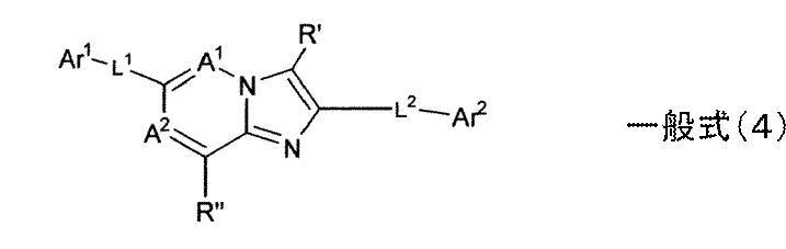
ただし、前記一般式(4)中、A1及びA2は、それぞれ独立に、窒素原子又は炭素原子である。
Ar1は、置換もしくは無置換の核炭素数6~60のアリール基、又は置換もしくは無置換の核炭素数3~60のヘテロアリール基である。Ar2は、水素原子、置換もしくは無置換の核炭素数6~60のアリール基、置換もしくは無置換の核炭素数3~60のヘテロアリール基、置換もしくは無置換の炭素数1~20のアルキル基、又は置換もしくは無置換の炭素数1~20のアルコキシ基である。ただし、Ar1及びAr2のいずれか一方は、置換もしくは無置換の核炭素数10~60の縮合環基、又は置換もしくは無置換の核炭素数3~60のモノヘテロ縮合環基である。
L1及びL2は、それぞれ独立に、単結合、置換もしくは無置換の核炭素数6~60のアリーレン基、置換もしくは無置換の核炭素数3~60のヘテロアリーレン基、又は置換もしくは無置換のフルオレニレン基である。
R’及びR”は、それぞれ独立に、水素原子、置換もしくは無置換の核炭素数6~60のアリール基、置換もしくは無置換の核炭素数3~60のヘテロアリール基、置換もしくは無置換の炭素数1~20のアルキル基、又は置換もしくは無置換の炭素数1~20のアルコキシ基であり、R’及びR”は同一でも異なっていてもよい。 The organic electroluminescent element according to claim 2, wherein the nitrogen-containing heterocyclic derivative represented by the general formula (3) is a nitrogen-containing heterocyclic derivative represented by the following general formula (4).
However, in the general formula (4), A 1 and A 2 are each independently a nitrogen atom or a carbon atom.
Ar 1 is a substituted or unsubstituted aryl group having 6 to 60 nuclear carbon atoms, or a substituted or unsubstituted heteroaryl group having 3 to 60 nuclear carbon atoms. Ar 2 represents a hydrogen atom, a substituted or unsubstituted aryl group having 6 to 60 nuclear carbon atoms, a substituted or unsubstituted heteroaryl group having 3 to 60 nuclear carbon atoms, or a substituted or unsubstituted alkyl group having 1 to 20 carbon atoms. Or a substituted or unsubstituted alkoxy group having 1 to 20 carbon atoms. However, one of Ar 1 and Ar 2 is a substituted or unsubstituted condensed ring group having 10 to 60 nuclear carbon atoms, or a substituted or unsubstituted monoheterocondensed ring group having 3 to 60 nuclear carbon atoms.
L 1 and L 2 are each independently a single bond, a substituted or unsubstituted arylene group having 6 to 60 nuclear carbon atoms, a substituted or unsubstituted heteroarylene group having 3 to 60 nuclear carbon atoms, or a substituted or unsubstituted group. Of the fluorenylene group.
R ′ and R ″ each independently represents a hydrogen atom, a substituted or unsubstituted aryl group having 6 to 60 nuclear carbon atoms, a substituted or unsubstituted heteroaryl group having 3 to 60 nuclear carbon atoms, substituted or unsubstituted An alkyl group having 1 to 20 carbon atoms, or a substituted or unsubstituted alkoxy group having 1 to 20 carbon atoms, and R ′ and R ″ may be the same or different. - 一般式(1)、(3)及び(4)の少なくともいずれかで表される含窒素複素環誘導体において、L1及びL2の少なくともいずれかが、下記構造式で表される基から選択される請求項1から3のいずれかに記載の有機電界発光素子。
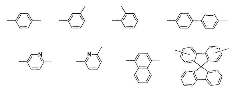
In the nitrogen-containing heterocyclic derivative represented by at least one of the general formulas (1), (3), and (4), at least one of L 1 and L 2 is selected from the group represented by the following structural formula The organic electroluminescent element according to claim 1.
- 一般式(1)、(3)及び(4)の少なくともいずれかで表される含窒素複素環誘導体において、Ar1が、下記一般式(5)から(14)のいずれかで表される基である請求項1から4のいずれかに記載の有機電界発光素子。

ただし、前記式中、R1~R92は、それぞれ独立して、水素原子、ハロゲン原子、置換もしくは無置換の炭素数1~20のアルキル基、置換もしくは無置換の炭素数1~20のアルコキシ基、置換もしくは無置換の核炭素数6~40のアリールオキシ基、置換もしくは無置換の核炭素数12~80のジアリールアミノ基、置換もしくは無置換の核炭素数6~40のアリール基、置換もしくは無置換の核炭素数3~40のヘテロアリール基、又は置換もしくは無置換の核炭素数18~120のジアリールアミノアリール基を表す。L3は、単結合、又は下記構造式で表される置換基を表す。

In the above formulae, R 1 to R 92 each independently represents a hydrogen atom, a halogen atom, a substituted or unsubstituted alkyl group having 1 to 20 carbon atoms, or a substituted or unsubstituted alkoxy group having 1 to 20 carbon atoms. Group, substituted or unsubstituted aryloxy group having 6 to 40 nuclear carbon atoms, substituted or unsubstituted diarylamino group having 12 to 80 nuclear carbon atoms, substituted or unsubstituted aryl group having 6 to 40 nuclear carbon atoms, substituted Alternatively, it represents an unsubstituted heteroaryl group having 3 to 40 nuclear carbon atoms, or a substituted or unsubstituted diarylaminoaryl group having 18 to 120 nuclear carbon atoms. L 3 represents a single bond or a substituent represented by the following structural formula.
- 一般式(2)で表される化合物が、下記一般式(15a-3)で表される化合物である請求項1から5のいずれかに記載の有機電界発光素子。

ただし、前記一般式(15a-3)中、X1、X2及びX4は、それぞれ独立に、炭素原子又は窒素原子を表す。R41、R42、R43、R44、R45及びR46は、それぞれ独立に水素原子又は置換基を表す。X53及びX54は、それぞれ独立に、炭素原子又は窒素原子を表し、X53及びX54を含有する5員環骨格に含まれる窒素原子の数は、1又は2である。R75は、水素原子又は置換基を表す。Lは、単結合又は2価の連結基を表す。 The organic electroluminescence device according to any one of claims 1 to 5, wherein the compound represented by the general formula (2) is a compound represented by the following general formula (15a-3).
However, in the general formula (15a-3), X 1 , X 2 and X 4 each independently represent a carbon atom or a nitrogen atom. R 41, R 42, R 43 , R 44, R 45 and R 46 each independently represent a hydrogen atom or a substituent. X 53 and X 54 each independently represent a carbon atom or a nitrogen atom, and the number of nitrogen atoms contained in the 5-membered ring skeleton containing X 53 and X 54 is 1 or 2. R 75 represents a hydrogen atom or a substituent. L represents a single bond or a divalent linking group. - 一般式(2)で表される部分構造を有する多座配位子の金属錯体化合物、及び一般式(15a-3)で表される四座配位子の白金錯体化合物の少なくとも一種が、発光層に含有される請求項1から6のいずれかに記載の有機電界発光素子。 At least one of a metal complex compound of a multidentate ligand having a partial structure represented by the general formula (2) and a platinum complex compound of a tetradentate ligand represented by the general formula (15a-3) is a light emitting layer The organic electroluminescent element according to claim 1, which is contained in the organic electroluminescent element.
- 一般式(2)で表される部分構造を有する多座配位子の金属錯体化合物、及び一般式(15a-3)で表される四座配位子の白金錯体化合物の少なくとも一種と、少なくとも一種のホスト材料が、発光層に含有される請求項1から7のいずれかに記載の有機電界発光素子。 At least one and at least one kind of a polydentate metal complex compound having a partial structure represented by the general formula (2) and a tetradentate platinum complex compound represented by the general formula (15a-3) The organic electroluminescent element according to claim 1, wherein the host material is contained in the light emitting layer.
- 少なくとも一種のホスト材料が正孔輸送性である請求項8に記載の有機電界発光素子。 9. The organic electroluminescent device according to claim 8, wherein at least one kind of host material has hole transportability.
- 含窒素複素環誘導体が、電子注入材料及び電子輸送材料の少なくともいずれかとして用いられている請求項1から9のいずれかに記載の有機電界発光素子。 The organic electroluminescent element according to any one of claims 1 to 9, wherein the nitrogen-containing heterocyclic derivative is used as at least one of an electron injection material and an electron transport material.
- 含窒素複素環誘導体を含有する層が、還元性ドーパントを含有する請求項1から10のいずれかに記載の有機電界発光素子。 The organic electroluminescent element according to claim 1, wherein the layer containing a nitrogen-containing heterocyclic derivative contains a reducing dopant.
- 還元性ドーパントが、アルカリ金属、アルカリ土類金属、希土類金属、アルカリ金属の酸化物、アルカリ金属のハロゲン化物、アルカリ土類金属の酸化物、アルカリ土類金属のハロゲン化物、希土類金属の酸化物、希土類金属のハロゲン化物、アルカリ金属の有機錯体、アルカリ土類金属の有機錯体、及び希土類金属の有機錯体から選ばれる少なくとも一種である請求項11に記載の有機電界発光素子。 The reducing dopant is alkali metal, alkaline earth metal, rare earth metal, alkali metal oxide, alkali metal halide, alkaline earth metal oxide, alkaline earth metal halide, rare earth metal oxide, The organic electroluminescence device according to claim 11, wherein the organic electroluminescence device is at least one selected from a rare earth metal halide, an alkali metal organic complex, an alkaline earth metal organic complex, and a rare earth metal organic complex.
Priority Applications (4)
| Application Number | Priority Date | Filing Date | Title |
|---|---|---|---|
| EP09838880.4A EP2381501B1 (en) | 2009-01-22 | 2009-12-25 | Organic electroluminescent element |
| US13/132,046 US20110227058A1 (en) | 2009-01-22 | 2009-12-25 | Organic electroluminescence element |
| CN200980155173.8A CN102292840B (en) | 2009-01-22 | 2009-12-25 | Organic electroluminescent element |
| KR1020117016226A KR101659104B1 (en) | 2009-01-22 | 2009-12-25 | Organic electroluminescent element |
Applications Claiming Priority (2)
| Application Number | Priority Date | Filing Date | Title |
|---|---|---|---|
| JP2009-012389 | 2009-01-22 | ||
| JP2009012389A JP5210187B2 (en) | 2009-01-22 | 2009-01-22 | Organic electroluminescence device |
Publications (1)
| Publication Number | Publication Date |
|---|---|
| WO2010084690A1 true WO2010084690A1 (en) | 2010-07-29 |
Family
ID=42355753
Family Applications (1)
| Application Number | Title | Priority Date | Filing Date |
|---|---|---|---|
| PCT/JP2009/071557 WO2010084690A1 (en) | 2009-01-22 | 2009-12-25 | Organic electroluminescent element |
Country Status (7)
| Country | Link |
|---|---|
| US (1) | US20110227058A1 (en) |
| EP (1) | EP2381501B1 (en) |
| JP (1) | JP5210187B2 (en) |
| KR (1) | KR101659104B1 (en) |
| CN (1) | CN102292840B (en) |
| TW (1) | TWI480358B (en) |
| WO (1) | WO2010084690A1 (en) |
Cited By (6)
| Publication number | Priority date | Publication date | Assignee | Title |
|---|---|---|---|---|
| US8716282B2 (en) | 2009-10-30 | 2014-05-06 | Janssen Pharmaceutica Nv | Imidazo[1,2-b]pyridazine derivatives and their use as PDE10 inhibitors |
| US8859543B2 (en) | 2010-03-09 | 2014-10-14 | Janssen Pharmaceutica Nv | Imidazo[1,2-a]pyrazine derivatives and their use for the prevention or treatment of neurological, psychiatric and metabolic disorders and diseases |
| CN104744349A (en) * | 2010-11-04 | 2015-07-01 | 捷恩智株式会社 | Electron transport material and organic electroluminescence element using same |
| US9550784B2 (en) | 2012-07-09 | 2017-01-24 | Beerse Pharmaceutica NV | Inhibitors of phosphodiesterase 10 enzyme |
| US9669035B2 (en) | 2012-06-26 | 2017-06-06 | Janssen Pharmaceutica Nv | Combinations comprising PDE 2 inhibitors such as 1-aryl-4-methyl-[1,2,4]triazolo-[4,3-A]]quinoxaline compounds and PDE 10 inhibitors for use in the treatment of neurological of metabolic disorders |
| US10604523B2 (en) | 2011-06-27 | 2020-03-31 | Janssen Pharmaceutica Nv | 1-aryl-4-methyl-[1,2,4]triazolo[4,3-a]quinoxaline derivatives |
Families Citing this family (43)
| Publication number | Priority date | Publication date | Assignee | Title |
|---|---|---|---|---|
| JP5627883B2 (en) * | 2009-01-07 | 2014-11-19 | ユー・ディー・シー アイルランド リミテッド | Organic electroluminescence device |
| TWI638807B (en) * | 2009-04-28 | 2018-10-21 | 環球展覽公司 | Iridium complex with methyl-d3 substitution |
| WO2011137429A2 (en) | 2010-04-30 | 2011-11-03 | Arizona Board Of Regents Acting For And On Behalf Of Arizona State University | Synthesis of four coordinated palladium complexes and their applications in light emitting devices thereof |
| JP5794771B2 (en) * | 2010-09-30 | 2015-10-14 | ユー・ディー・シー アイルランド リミテッド | Material for organic electroluminescent element, film, light emitting layer, organic electroluminescent element, and method for producing organic electroluminescent element |
| KR102091393B1 (en) * | 2012-01-16 | 2020-03-23 | 메르크 파텐트 게엠베하 | Organic metal complexes |
| JP6118034B2 (en) | 2012-02-06 | 2017-04-19 | ユー・ディー・シー アイルランド リミテッド | ORGANIC ELECTROLUMINESCENT ELEMENT, COMPOUND USABLE FOR THE SAME, ORGANIC ELECTROLUMINESCENT ELEMENT MATERIAL, AND LIGHT EMITTING DEVICE, DISPLAY DEVICE AND LIGHTING DEVICE USING THE ELEMENT |
| KR102124227B1 (en) | 2012-09-24 | 2020-06-17 | 아리조나 보드 오브 리젠츠 온 비하프 오브 아리조나 스테이트 유니버시티 | Metal compounds, methods, and uses thereof |
| CN103709180B (en) * | 2012-09-29 | 2016-12-21 | 昆山维信诺显示技术有限公司 | Containing the condensed-nuclei aromatics derivant of imidazo [1,2-a] pyridine groups and the application in OLED thereof |
| WO2014109814A2 (en) | 2012-10-26 | 2014-07-17 | Arizona Board Of Regents Acting For And On Behalf Of Arizona State University | Metal complexes, methods, and uses thereof |
| CN104232076B (en) | 2013-06-10 | 2019-01-15 | 代表亚利桑那大学的亚利桑那校董会 | Four tooth metal complex of phosphorescence with improved emission spectrum |
| US9130182B2 (en) * | 2013-06-28 | 2015-09-08 | Semiconductor Energy Laboratory Co., Ltd. | Light-emitting element, lighting device, light-emitting device, and electronic device |
| JP6804823B2 (en) * | 2013-10-14 | 2020-12-23 | アリゾナ・ボード・オブ・リージェンツ・オン・ビハーフ・オブ・アリゾナ・ステイト・ユニバーシティーArizona Board of Regents on behalf of Arizona State University | Platinum complex and device |
| US10020455B2 (en) | 2014-01-07 | 2018-07-10 | Arizona Board Of Regents On Behalf Of Arizona State University | Tetradentate platinum and palladium complex emitters containing phenyl-pyrazole and its analogues |
| US9941479B2 (en) | 2014-06-02 | 2018-04-10 | Arizona Board Of Regents On Behalf Of Arizona State University | Tetradentate cyclometalated platinum complexes containing 9,10-dihydroacridine and its analogues |
| US9923155B2 (en) | 2014-07-24 | 2018-03-20 | Arizona Board Of Regents On Behalf Of Arizona State University | Tetradentate platinum (II) complexes cyclometalated with functionalized phenyl carbene ligands and their analogues |
| WO2016025921A1 (en) | 2014-08-15 | 2016-02-18 | Arizona Board Of Regents On Behalf Of Arizona State University | Non-platinum metal complexes for excimer based single dopant white organic light emitting diodes |
| US11329244B2 (en) | 2014-08-22 | 2022-05-10 | Arizona Board Of Regents On Behalf Of Arizona State University | Organic light-emitting diodes with fluorescent and phosphorescent emitters |
| WO2016029186A1 (en) | 2014-08-22 | 2016-02-25 | Arizona Board Of Regents On Behalf Of Arizona State University | Metal-assisted delayed fluorescent materials as co-host materials for fluorescent oleds |
| US9865825B2 (en) | 2014-11-10 | 2018-01-09 | Arizona Board Of Regents On Behalf Of Arizona State University | Emitters based on octahedral metal complexes |
| US10033003B2 (en) | 2014-11-10 | 2018-07-24 | Arizona Board Of Regents On Behalf Of Arizona State University | Tetradentate metal complexes with carbon group bridging ligands |
| US9879039B2 (en) | 2015-06-03 | 2018-01-30 | Arizona Board Of Regents On Behalf Of Arizona State University | Tetradentate and octahedral metal complexes containing naphthyridinocarbazole and its analogues |
| WO2016197019A1 (en) | 2015-06-04 | 2016-12-08 | Jian Li | Transparent electroluminescent devices with controlled one-side emissive displays |
| US11335865B2 (en) | 2016-04-15 | 2022-05-17 | Arizona Board Of Regents On Behalf Of Arizona State University | OLED with multi-emissive material layer |
| EP3266790B1 (en) * | 2016-07-05 | 2019-11-06 | Samsung Electronics Co., Ltd | Organometallic compound, organic light-emitting device including the same, and diagnostic composition including the organometallic compound |
| US10177323B2 (en) | 2016-08-22 | 2019-01-08 | Arizona Board Of Regents On Behalf Of Arizona State University | Tetradentate platinum (II) and palladium (II) complexes and octahedral iridium complexes employing azepine functional groups and their analogues |
| WO2018071697A1 (en) | 2016-10-12 | 2018-04-19 | Jian Li | Narrow band red phosphorescent tetradentate platinum (ii) complexes |
| US11183670B2 (en) | 2016-12-16 | 2021-11-23 | Arizona Board Of Regents On Behalf Of Arizona State University | Organic light emitting diode with split emissive layer |
| KR20190139835A (en) | 2017-01-27 | 2019-12-18 | 아리조나 보드 오브 리젠츠 온 비하프 오브 아리조나 스테이트 유니버시티 | Metal assisted delayed fluorescence emitter using pyrido-pyrrolo-acridine and analogs |
| US11101435B2 (en) | 2017-05-19 | 2021-08-24 | Arizona Board Of Regents On Behalf Of Arizona State University | Tetradentate platinum and palladium complexes based on biscarbazole and analogues |
| US10516117B2 (en) | 2017-05-19 | 2019-12-24 | Arizona Board Of Regents On Behalf Of Arizona State University | Metal-assisted delayed fluorescent emttters employing benzo-imidazo-phenanthridine and analogues |
| WO2019079505A1 (en) | 2017-10-17 | 2019-04-25 | Jian Li | Hole-blocking materials for organic light emitting diodes |
| WO2019079508A2 (en) | 2017-10-17 | 2019-04-25 | Jian Li | Phosphorescent excimers with preferred molecular orientation as monochromatic emitters for display and lighting applications |
| KR102027523B1 (en) * | 2017-12-22 | 2019-10-01 | 엘지디스플레이 주식회사 | Organic light emitting diode and organic light emittind display device having the same |
| KR102027512B1 (en) * | 2017-12-22 | 2019-10-01 | 엘지디스플레이 주식회사 | Organic light emitting diode and organic light emittind display device having the same |
| EP3762470B1 (en) * | 2018-04-11 | 2023-11-29 | Kyulux, Inc. | Top-emitting printed display with quantum dots and thermally activated delayed fluorescence molecules |
| CN109535205B (en) * | 2018-12-30 | 2021-10-08 | 浙江工业大学 | Platinum complex containing tetradentate ligand and aryloxy derivative |
| US11878988B2 (en) | 2019-01-24 | 2024-01-23 | Arizona Board Of Regents On Behalf Of Arizona State University | Blue phosphorescent emitters employing functionalized imidazophenthridine and analogues |
| US11594691B2 (en) | 2019-01-25 | 2023-02-28 | Arizona Board Of Regents On Behalf Of Arizona State University | Light outcoupling efficiency of phosphorescent OLEDs by mixing horizontally aligned fluorescent emitters |
| KR102259315B1 (en) * | 2019-09-25 | 2021-05-31 | 엘지디스플레이 주식회사 | Organic light emitting diode and organic light emittind display device having the same |
| KR102332549B1 (en) * | 2019-09-25 | 2021-12-01 | 엘지디스플레이 주식회사 | Organic light emitting diode and organic light emittind display device having the same |
| KR102150870B1 (en) * | 2019-09-25 | 2020-09-02 | 엘지디스플레이 주식회사 | Organic light emitting diode and organic light emittind display device having the same |
| US11785838B2 (en) | 2019-10-02 | 2023-10-10 | Arizona Board Of Regents On Behalf Of Arizona State University | Green and red organic light-emitting diodes employing excimer emitters |
| US11945985B2 (en) | 2020-05-19 | 2024-04-02 | Arizona Board Of Regents On Behalf Of Arizona State University | Metal assisted delayed fluorescent emitters for organic light-emitting diodes |
Citations (18)
| Publication number | Priority date | Publication date | Assignee | Title |
|---|---|---|---|---|
| JPH09180883A (en) | 1995-10-27 | 1997-07-11 | Toyota Central Res & Dev Lab Inc | Micro-light resonating organic electroluminescent element |
| JP2002235076A (en) | 2001-02-09 | 2002-08-23 | Fuji Photo Film Co Ltd | Transition metal complex and light emission element material comprising the same, and light emission element |
| WO2004028217A1 (en) * | 2002-09-20 | 2004-04-01 | Idemitsu Kosan Co., Ltd. | Organic electroluminescent element |
| JP2004127795A (en) | 2002-10-04 | 2004-04-22 | Sony Corp | Display element and display device using the display device |
| WO2004034751A1 (en) * | 2002-10-09 | 2004-04-22 | Idemitsu Kosan Co., Ltd. | Organic electroluminescent device |
| JP2004515506A (en) | 2000-12-07 | 2004-05-27 | キヤノン株式会社 | Deuterated organic semiconductor compounds for optoelectronic devices |
| JP2004214179A (en) | 2002-12-17 | 2004-07-29 | Fuji Photo Film Co Ltd | Organic electroluminescent element |
| JP2004217547A (en) * | 2003-01-14 | 2004-08-05 | Idemitsu Kosan Co Ltd | Nitrogen-containing heterocyclic derivative and organic electroluminescent element using the same |
| JP2004221065A (en) | 2002-12-27 | 2004-08-05 | Fuji Photo Film Co Ltd | Organic electroluminescent element |
| JP2004221062A (en) | 2002-12-27 | 2004-08-05 | Fuji Photo Film Co Ltd | Organic electroluminescent element |
| JP2004221068A (en) | 2002-12-27 | 2004-08-05 | Fuji Photo Film Co Ltd | Organic electroluminescent element |
| JP2004327313A (en) | 2003-04-25 | 2004-11-18 | Fuji Photo Film Co Ltd | Organic el device |
| WO2005076669A1 (en) * | 2004-02-09 | 2005-08-18 | Idemitsu Kosan Co., Ltd. | Organic electroluminescent device |
| WO2005088726A1 (en) | 2004-03-12 | 2005-09-22 | Japan Science And Technology Agency | Amorphous oxide and thin film transistor |
| JP2006165529A (en) | 2004-11-10 | 2006-06-22 | Canon Inc | Amorphous oxide and field effect transistor |
| JP2008126130A (en) | 2006-11-20 | 2008-06-05 | Hitachi Koki Co Ltd | Rotor for centrifuge and centrifuge equipped with it |
| US20080237598A1 (en) | 2007-03-27 | 2008-10-02 | Masaya Nakayama | Thin film field effect transistor and display |
| JP2009283891A (en) * | 2008-04-22 | 2009-12-03 | Fujifilm Corp | Organic electroluminescence device, novel platinum complex compound and novel compound capable of being ligand thereof |
Family Cites Families (7)
| Publication number | Priority date | Publication date | Assignee | Title |
|---|---|---|---|---|
| JP4041624B2 (en) | 1999-07-21 | 2008-01-30 | 三井化学株式会社 | Organic electroluminescence device |
| WO2004063159A1 (en) * | 2003-01-10 | 2004-07-29 | Idemitsu Kosan Co., Ltd. | Nitrogenous heterocyclic derivative and organic electroluminescent element employing the same |
| JP4500735B2 (en) * | 2004-09-22 | 2010-07-14 | 富士フイルム株式会社 | Organic electroluminescence device |
| JP4531509B2 (en) * | 2004-09-27 | 2010-08-25 | 富士フイルム株式会社 | Light emitting element |
| US20080000153A1 (en) * | 2005-01-07 | 2008-01-03 | Nobuo Sugiyama | Temporary Structural Body for Seeding and Planting |
| JP5006606B2 (en) | 2006-09-13 | 2012-08-22 | 双葉電子工業株式会社 | COMPOUND FOR ORGANIC EL ELEMENT AND ORGANIC EL ELEMENT |
| JP2009076865A (en) * | 2007-08-29 | 2009-04-09 | Fujifilm Corp | Organic electroluminescence device |
-
2009
- 2009-01-22 JP JP2009012389A patent/JP5210187B2/en active Active
- 2009-12-25 US US13/132,046 patent/US20110227058A1/en not_active Abandoned
- 2009-12-25 CN CN200980155173.8A patent/CN102292840B/en active Active
- 2009-12-25 EP EP09838880.4A patent/EP2381501B1/en active Active
- 2009-12-25 WO PCT/JP2009/071557 patent/WO2010084690A1/en active Application Filing
- 2009-12-25 KR KR1020117016226A patent/KR101659104B1/en active IP Right Grant
- 2009-12-30 TW TW098145791A patent/TWI480358B/en active
Patent Citations (18)
| Publication number | Priority date | Publication date | Assignee | Title |
|---|---|---|---|---|
| JPH09180883A (en) | 1995-10-27 | 1997-07-11 | Toyota Central Res & Dev Lab Inc | Micro-light resonating organic electroluminescent element |
| JP2004515506A (en) | 2000-12-07 | 2004-05-27 | キヤノン株式会社 | Deuterated organic semiconductor compounds for optoelectronic devices |
| JP2002235076A (en) | 2001-02-09 | 2002-08-23 | Fuji Photo Film Co Ltd | Transition metal complex and light emission element material comprising the same, and light emission element |
| WO2004028217A1 (en) * | 2002-09-20 | 2004-04-01 | Idemitsu Kosan Co., Ltd. | Organic electroluminescent element |
| JP2004127795A (en) | 2002-10-04 | 2004-04-22 | Sony Corp | Display element and display device using the display device |
| WO2004034751A1 (en) * | 2002-10-09 | 2004-04-22 | Idemitsu Kosan Co., Ltd. | Organic electroluminescent device |
| JP2004214179A (en) | 2002-12-17 | 2004-07-29 | Fuji Photo Film Co Ltd | Organic electroluminescent element |
| JP2004221065A (en) | 2002-12-27 | 2004-08-05 | Fuji Photo Film Co Ltd | Organic electroluminescent element |
| JP2004221062A (en) | 2002-12-27 | 2004-08-05 | Fuji Photo Film Co Ltd | Organic electroluminescent element |
| JP2004221068A (en) | 2002-12-27 | 2004-08-05 | Fuji Photo Film Co Ltd | Organic electroluminescent element |
| JP2004217547A (en) * | 2003-01-14 | 2004-08-05 | Idemitsu Kosan Co Ltd | Nitrogen-containing heterocyclic derivative and organic electroluminescent element using the same |
| JP2004327313A (en) | 2003-04-25 | 2004-11-18 | Fuji Photo Film Co Ltd | Organic el device |
| WO2005076669A1 (en) * | 2004-02-09 | 2005-08-18 | Idemitsu Kosan Co., Ltd. | Organic electroluminescent device |
| WO2005088726A1 (en) | 2004-03-12 | 2005-09-22 | Japan Science And Technology Agency | Amorphous oxide and thin film transistor |
| JP2006165529A (en) | 2004-11-10 | 2006-06-22 | Canon Inc | Amorphous oxide and field effect transistor |
| JP2008126130A (en) | 2006-11-20 | 2008-06-05 | Hitachi Koki Co Ltd | Rotor for centrifuge and centrifuge equipped with it |
| US20080237598A1 (en) | 2007-03-27 | 2008-10-02 | Masaya Nakayama | Thin film field effect transistor and display |
| JP2009283891A (en) * | 2008-04-22 | 2009-12-03 | Fujifilm Corp | Organic electroluminescence device, novel platinum complex compound and novel compound capable of being ligand thereof |
Non-Patent Citations (4)
| Title |
|---|
| AKIO YAMAMOTO: "YUHKI KINZOKU KAGAKU-KISO TO OUYOU", 1982, SHOKABO PUBLISHING CO., LTD. |
| H. YERSIN: "Photochemistry and Photophysics of Coordination Compounds", 1987, SPRINGER-VERLAG CO. |
| MONTHLY DISPLAY, September 2000 (2000-09-01), pages 33 - 37 |
| See also references of EP2381501A4 |
Cited By (7)
| Publication number | Priority date | Publication date | Assignee | Title |
|---|---|---|---|---|
| US8716282B2 (en) | 2009-10-30 | 2014-05-06 | Janssen Pharmaceutica Nv | Imidazo[1,2-b]pyridazine derivatives and their use as PDE10 inhibitors |
| US8859543B2 (en) | 2010-03-09 | 2014-10-14 | Janssen Pharmaceutica Nv | Imidazo[1,2-a]pyrazine derivatives and their use for the prevention or treatment of neurological, psychiatric and metabolic disorders and diseases |
| CN104744349A (en) * | 2010-11-04 | 2015-07-01 | 捷恩智株式会社 | Electron transport material and organic electroluminescence element using same |
| CN104744349B (en) * | 2010-11-04 | 2017-09-22 | 捷恩智株式会社 | Electron transport material and use its organic electroluminescent element |
| US10604523B2 (en) | 2011-06-27 | 2020-03-31 | Janssen Pharmaceutica Nv | 1-aryl-4-methyl-[1,2,4]triazolo[4,3-a]quinoxaline derivatives |
| US9669035B2 (en) | 2012-06-26 | 2017-06-06 | Janssen Pharmaceutica Nv | Combinations comprising PDE 2 inhibitors such as 1-aryl-4-methyl-[1,2,4]triazolo-[4,3-A]]quinoxaline compounds and PDE 10 inhibitors for use in the treatment of neurological of metabolic disorders |
| US9550784B2 (en) | 2012-07-09 | 2017-01-24 | Beerse Pharmaceutica NV | Inhibitors of phosphodiesterase 10 enzyme |
Also Published As
| Publication number | Publication date |
|---|---|
| TW201033329A (en) | 2010-09-16 |
| JP2010171205A (en) | 2010-08-05 |
| CN102292840B (en) | 2014-08-13 |
| KR101659104B1 (en) | 2016-09-22 |
| TWI480358B (en) | 2015-04-11 |
| EP2381501B1 (en) | 2014-07-23 |
| CN102292840A (en) | 2011-12-21 |
| JP5210187B2 (en) | 2013-06-12 |
| EP2381501A4 (en) | 2012-12-19 |
| KR20110114569A (en) | 2011-10-19 |
| EP2381501A1 (en) | 2011-10-26 |
| US20110227058A1 (en) | 2011-09-22 |
Similar Documents
| Publication | Publication Date | Title |
|---|---|---|
| JP5210187B2 (en) | Organic electroluminescence device | |
| JP2010278354A (en) | Organic electroluminescent element | |
| JP4850521B2 (en) | Organic electroluminescence device | |
| US8294361B2 (en) | Organic electric field light-emitting element | |
| JP5324513B2 (en) | Organic electroluminescence device | |
| JP2008109085A (en) | Organic electroluminescent element | |
| WO2011021433A1 (en) | Organic electroluminescent element | |
| JP2007287652A (en) | Light-emitting element | |
| KR102238719B1 (en) | Organic electroluminescence element | |
| JP5833322B2 (en) | Organic electroluminescent device and manufacturing method thereof | |
| WO2010140482A1 (en) | Organic electroluminescent device | |
| JP5670223B2 (en) | Organic electroluminescence device | |
| JP5572004B2 (en) | White organic electroluminescence device | |
| JP5761962B2 (en) | Organic electroluminescence device | |
| JP5649327B2 (en) | Organic electroluminescence device | |
| JP2011192829A (en) | Organic electroluminescent element | |
| KR101989746B1 (en) | White organic electroluminescence element | |
| JP2011034805A (en) | Organic electroluminescent element and evaluation method of the same | |
| JP2010157606A (en) | Organic electroluminescent element | |
| JP5890504B2 (en) | Organic electroluminescence device | |
| JP2010171204A (en) | Organic electric field light-emitting element |
Legal Events
| Date | Code | Title | Description |
|---|---|---|---|
| WWE | Wipo information: entry into national phase |
Ref document number: 200980155173.8 Country of ref document: CN |
|
| 121 | Ep: the epo has been informed by wipo that ep was designated in this application |
Ref document number: 09838880 Country of ref document: EP Kind code of ref document: A1 |
|
| WWE | Wipo information: entry into national phase |
Ref document number: 13132046 Country of ref document: US |
|
| WWE | Wipo information: entry into national phase |
Ref document number: 2009838880 Country of ref document: EP |
|
| ENP | Entry into the national phase |
Ref document number: 20117016226 Country of ref document: KR Kind code of ref document: A |
|
| NENP | Non-entry into the national phase |
Ref country code: DE |