WO2010082576A1 - 接触子及びその製造方法、ならびに前記接触子を備えた接続装置 - Google Patents
接触子及びその製造方法、ならびに前記接触子を備えた接続装置 Download PDFInfo
- Publication number
- WO2010082576A1 WO2010082576A1 PCT/JP2010/050261 JP2010050261W WO2010082576A1 WO 2010082576 A1 WO2010082576 A1 WO 2010082576A1 JP 2010050261 W JP2010050261 W JP 2010050261W WO 2010082576 A1 WO2010082576 A1 WO 2010082576A1
- Authority
- WO
- WIPO (PCT)
- Prior art keywords
- elastic arm
- tip
- width
- width dimension
- contact
- Prior art date
- Legal status (The legal status is an assumption and is not a legal conclusion. Google has not performed a legal analysis and makes no representation as to the accuracy of the status listed.)
- Ceased
Links
Images



Classifications
-
- G—PHYSICS
- G01—MEASURING; TESTING
- G01R—MEASURING ELECTRIC VARIABLES; MEASURING MAGNETIC VARIABLES
- G01R3/00—Apparatus or processes specially adapted for the manufacture or maintenance of measuring instruments, e.g. of probe tips
-
- G—PHYSICS
- G01—MEASURING; TESTING
- G01R—MEASURING ELECTRIC VARIABLES; MEASURING MAGNETIC VARIABLES
- G01R1/00—Details of instruments or arrangements of the types included in groups G01R5/00 - G01R13/00 and G01R31/00
- G01R1/02—General constructional details
- G01R1/06—Measuring leads; Measuring probes
- G01R1/067—Measuring probes
- G01R1/06711—Probe needles; Cantilever beams; "Bump" contacts; Replaceable probe pins
- G01R1/06716—Elastic
-
- G—PHYSICS
- G01—MEASURING; TESTING
- G01R—MEASURING ELECTRIC VARIABLES; MEASURING MAGNETIC VARIABLES
- G01R1/00—Details of instruments or arrangements of the types included in groups G01R5/00 - G01R13/00 and G01R31/00
- G01R1/02—General constructional details
- G01R1/06—Measuring leads; Measuring probes
- G01R1/067—Measuring probes
- G01R1/06711—Probe needles; Cantilever beams; "Bump" contacts; Replaceable probe pins
- G01R1/06733—Geometry aspects
-
- G—PHYSICS
- G01—MEASURING; TESTING
- G01R—MEASURING ELECTRIC VARIABLES; MEASURING MAGNETIC VARIABLES
- G01R1/00—Details of instruments or arrangements of the types included in groups G01R5/00 - G01R13/00 and G01R31/00
- G01R1/02—General constructional details
- G01R1/06—Measuring leads; Measuring probes
- G01R1/067—Measuring probes
- G01R1/073—Multiple probes
- G01R1/07307—Multiple probes with individual probe elements, e.g. needles, cantilever beams or bump contacts, fixed in relation to each other, e.g. bed of nails fixture or probe card
- G01R1/07342—Multiple probes with individual probe elements, e.g. needles, cantilever beams or bump contacts, fixed in relation to each other, e.g. bed of nails fixture or probe card the body of the probe being at an angle other than perpendicular to test object, e.g. probe card
-
- H—ELECTRICITY
- H01—ELECTRIC ELEMENTS
- H01R—ELECTRICALLY-CONDUCTIVE CONNECTIONS; STRUCTURAL ASSOCIATIONS OF A PLURALITY OF MUTUALLY-INSULATED ELECTRICAL CONNECTING ELEMENTS; COUPLING DEVICES; CURRENT COLLECTORS
- H01R13/00—Details of coupling devices of the kinds covered by groups H01R12/70 or H01R24/00 - H01R33/00
- H01R13/02—Contact members
- H01R13/22—Contacts for co-operating by abutting
- H01R13/24—Contacts for co-operating by abutting resilient; resiliently-mounted
- H01R13/2407—Contacts for co-operating by abutting resilient; resiliently-mounted characterized by the resilient means
- H01R13/2421—Contacts for co-operating by abutting resilient; resiliently-mounted characterized by the resilient means using coil springs
-
- H—ELECTRICITY
- H01—ELECTRIC ELEMENTS
- H01R—ELECTRICALLY-CONDUCTIVE CONNECTIONS; STRUCTURAL ASSOCIATIONS OF A PLURALITY OF MUTUALLY-INSULATED ELECTRICAL CONNECTING ELEMENTS; COUPLING DEVICES; CURRENT COLLECTORS
- H01R43/00—Apparatus or processes specially adapted for manufacturing, assembling, maintaining, or repairing of line connectors or current collectors or for joining electric conductors
- H01R43/16—Apparatus or processes specially adapted for manufacturing, assembling, maintaining, or repairing of line connectors or current collectors or for joining electric conductors for manufacturing contact members, e.g. by punching and by bending
Definitions
- the present invention relates to a contact including a wound conductive elastic arm and three-dimensionally formed upward from the proximal end to the distal end of the elastic arm, a method of manufacturing the same, and a connection device.
- Patent Document 1 discloses a contact of a spiral shape, and the width of the elastic arm (swirl portion) gradually narrows from the proximal end (root) to the distal end.
- FIG. 7 is a plan view of a contact showing a comparative example.
- the contact 1 is composed of a mount 2 and an elastic arm 3 extending from the mount 2.
- the elastic arm 3 gradually decreases in width from the proximal end 3a to the distal end 3b.
- the tip 3 b is provided at a position deviated from the core O of the elastic arm 3.
- the “drawing core” is defined as a point approximately equidistant from the peripheral edge of the elastic arm 3, or the approximate center of the elastic arm 3 or the position of the approximate center of gravity of the elastic arm 3.
- the reference line connecting the center O of the elastic arm 3 and the tip 3b is X0 in the plan view of FIG. 7, the reference line X0 is traversed outside the tip 1b when viewed from the center O
- a single elastic arm 3 formed with a width dimension of T3 at the transverse position and a width dimension of T4 at the transverse position transverse to the reference line X0 outside the drawing core O seen from the tip 3b
- One formed elastic arm 3 is provided.
- the width dimension T4 is smaller than the width dimension T3.
- the distance L1 between the center of the width of the tip 3b and the center of the width T4 of the elastic arm 3 is the center of the width of the tip 3b and the width of the elastic arm 3. It is larger than the distance L2 between the center of the dimension T3.
- the bending moment is an elastic arm 3 having a width T3.
- the position of the elastic arm 3 with the width dimension T4 is larger than the position of.
- the width dimension T4 is smaller than the width dimension T3, the torsional stress at the position of the width dimension T4 is strong when the elastic arm 3 is three-dimensionally formed as described above.
- the elastic arm 3 is three-dimensionally shaped so as to be steeply inclined from the vicinity of the position A of the width dimension T4 to the tip 3b. Further, the vicinity of the position A of the width dimension T4 is more easily inclined downward than the vicinity of the position B of the width dimension T3.
- contour lines Y of each part of the elastic arm 1 are illustrated on the surface of the elastic arm.
- this invention solves the said conventional subject, and it aims at providing the contact which was excellent in mechanical strength compared with before, its manufacturing method, and a connection apparatus.
- the present invention provides a contact including a conductive elastic arm electrically connected to an electrode of an electronic component,
- the elastic arm is formed in a winding shape in which the tip end is located inside the winding than the base end when viewed in a plan view, and is three-dimensionally formed upward from the base end toward the tip.
- the tip is provided at a position out of the core of the elastic arm,
- the width dimension is formed with a width dimension of T1 at the crossing position across the reference line X0 outside the tip when viewed from the drawing core
- the width dimension T2 is formed to be equal to or larger than the width dimension T1.
- the tip of the elastic arm is at a position out of the drawing core of the elastic arm.
- the “drawing core” is defined as a point approximately equidistant from the peripheral edge of the elastic arm, or the approximate center of the elastic arm 3 or the position of the approximate center of gravity.
- the width of the reference line X0 is traversed outside the tip as viewed from the drawing core at a transverse position.
- the elastic arm 12 is formed with a substantially constant width from the proximal end 12a to the distal end 12b.
- the tip 12 b of the elastic arm 12 is at a position out of the drawing core O.
- the base 12 crosses the reference line X0 outside the tip 12b when viewed from the core O
- a single elastic arm formed with a width T1 at the cross position, and a width T2 at the cross position across the reference line X0 outside the drawing core O seen from the tip 12b
- One elastic arm is provided.
- the distance L1 between the center of the width of the tip 12b and the center of the width T2 of the elastic arm 12 is the center of the width of the tip 12b and the width of the elastic arm 12. It is larger than the distance L2 between the center of the width dimension T1.
- the bending moment is the elastic arm 12 having the width dimension T1.
- the width T2 is made substantially the same as the width T1 unlike the comparative example shown in FIG.
- the torsional stress acting around the position C (see FIG. 2) of the width dimension T2 can be dispersed when the tip 12b is pushed upward and the elastic arm 12 is three-dimensionally formed.
- the position C of the width dimension T2 can be lifted up appropriately.
- mechanical strength can be strengthened with respect to elastic deformation of the elastic arm accompanying pressing movement of the electrode of an electronic component, and it can be a contact which is hard to be broken compared with before.
- the width of the elastic arm may be gradually expanded from the position of the width T1 (see FIG. 1) to the position of the width T2.
- the contact includes a conductive elastic arm electrically connected to the electrode of the electronic component.
- the contacts are formed in the configuration described above, In a plan view, the tip end of the elastic arm is located at a position deviated from the center of the electrode.
- the elastic arm is elastically deformed such that the tip of the elastic arm slides on the electrode surface in accordance with the pressing movement of the electrode.
- the oxide film on the surface of the electrode can be cut and conducted to ensure stable contact resistance.
- the elastic arm is formed with a projection that slides on the surface of the electrode as the electronic component is pressed and moved. More preferably, the projection is formed near the tip of the elastic arm.
- the present invention relates to a contact including a conductive elastic arm electrically connected to an electronic component having a spherical electrode,
- the elastic arm is formed in a winding shape in which the tip end is located inside the winding than the base end when viewed in a plan view, and is three-dimensionally formed upward from the base end toward the tip.
- the tip is provided at a position out of the core of the elastic arm,
- the transition line of the height from the proximal end to the tip is located on the linear curve or above the linear curve with respect to the linear curve drawn linearly at the position,
- a protrusion is formed at the tip toward the center of the drawing,
- the surface of the spherical electrode is slid along with the pressing movement of the electronic component, and a cut is made to the film formed on the surface of the spherical electrode by the protrusion to electrically connect the film. is there.
- the elastic arm is formed to have a substantially constant width from the proximal end to the distal end.
- a method of manufacturing a contact including a conductive elastic arm electrically connected to an electrode of an electronic component,
- the elastic arm is formed in a plane, and in this case, the distal end is formed in a winding shape located inside the winding than the proximal end, and the distal end is provided at a position deviated from the core of the elastic arm.
- the width dimension is T1 at the crossing position across the reference line X0 outside the tip when viewed from the drawing core.
- the acting torsional stress can be dispersed (reduced), and the position of the width dimension T2 of the elastic arm can be appropriately lifted upward.
- the contactor of the present invention and the connecting device provided with the contactor, excellent mechanical strength can be obtained. Furthermore, stable contact resistance can be secured to the spherical electrode etc. of the electronic component.
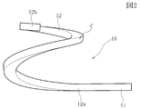
- FIG. 1 is a plan view showing a contact 10 according to an embodiment of the present invention
- FIG. 2 is a side view of the contact 10. As shown in FIG.
- the contacts 10 are formed by etching or plating.
- a thin plate-like copper film is etched to form the shape shown in FIG. 1, and the surface thereof is further plated with nickel, nickel-phosphorus, or the like.
- it can be formed of a laminate of copper and nickel, or a laminate of copper and nickel-phosphorus.
- nickel or nickel-phosphorus exerts an elastic function, and copper functions to lower the specific resistance.
- the contact 10 can be formed by plating a copper layer, or copper and nickel are continuously laminated to form a film, or copper and nickel-phosphorus are continuously laminated to form a film.
- a mount portion 11 having a predetermined thickness and a planar shape, and an elastic arm 12 extending from the mount portion 11 are integrally formed.
- the boundary between the elastic arm 12 and the mount portion 11 is the proximal end 12a, and the distal end 12b is located inside the winding pattern.
- an arm center line of the elastic arm 12 is indicated by ⁇ .
- the arm center line ⁇ is a continuous line connecting points that bisect the width dimension of the elastic arm 3 at each position of the elastic arm 3, and the arm center line ⁇ is also in a spiral shape.
- the drawing core O shown in FIG. 1 is a core of the elastic arm 12.
- the drawing core O is defined as a point approximately equidistant from the peripheral edge of the elastic arm 12, or the approximate center of the elastic arm 3, or the position of the approximate center of gravity of the elastic arm 3.
- the drawing core O may or may not coincide with the electrode center of the electronic component.
- the tip 12b of the elastic arm 12 is provided at a position deviated from the center O of the figure and also deviated from the center of the electrode.
- a space 15 is provided substantially at the center of the elastic arm 12, in which the drawing core O and the electrode center are located.
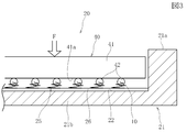
- connection device 20 comprising a contact 10 is shown.
- the connection device 20 has a base 21.
- the planar shape of the base 21 is, for example, a rectangular shape, and side walls 21a that rise substantially perpendicularly are formed on each of the four sides of the base 21.
- a region surrounded by the side wall portions 21 a of the four sides is a concave portion, and the upper surface of the bottom portion 21 b is a support surface 22.
- a connection sheet 25 is provided on the support surface 22.
- the connection sheet 25 has, for example, a configuration in which a plurality of contacts 10 are provided on the surface of a flexible base sheet 26.
- connection device 20 is provided with an electronic component 40.
- the electronic component 40 is an IC package or the like, and various electronic elements such as an IC bare chip are sealed in the main body 41.
- a plurality of spherical electrodes 42 are provided on the bottom surface 41 a of the main body 41, and each spherical electrode 42 is electrically connected to the circuit in the main body 41.
- the electronic component 40 is mounted in the recess of the base 10. At this time, the electronic component 40 is positioned such that the individual spherical electrodes 42 provided on the bottom surface 41 a of the main body 41 are placed on the contact 10.
- a lid (not shown) for pressing is provided on the base 21. When the lid is placed on the base 21, the electronic component 40 is pressed in the arrow F direction by the lid. By this pressing force, each spherical electrode 42 is pressed against the elastic arm 12 and the elastic arm 12 is crushed, and the spherical electrode 42 and the elastic arm 12 are separately conducted.
- the elastic arm 12 of the contact 10 in the present embodiment is three-dimensionally formed upward from the proximal end 12a to the distal end 12b as shown in FIG.
- the three-dimensional molding can be achieved by forming the contact 10 in the plane shown in FIG. 1, then bringing the push-up surface of the jig (pin) into contact with the vicinity of the tip 12b and pushing up the vicinity of the tip 12b with the jig. .
- a desired shape can be obtained regardless of the width and thickness of the elastic arm 12.
- the tip 12 b of the elastic arm 12 is at a position out of the drawing core O of the elastic arm 12. Further, the tip 12 b of the elastic arm 12 is located at a position deviated from the electrode center of the spherical electrode 42 in the connection device 20 shown in FIG. 3. Thereby, the elastic arm 12 is elastically deformed so that the tip 12b of the elastic arm 12 slides on the surface of the spherical electrode in accordance with the pressing movement of the spherical electrode 42 shown in FIG.
- FIG. 6A is a schematic view of the non-sliding contact
- FIG. 6B is a schematic view of the sliding contact. As shown in FIG.
- FIG. 6A when there is a contact orthogonal to the electrode center downward direction, even if the electrode is pushed downward, the contact is also pushed downward, and the contact does not slide on the electrode surface.
- FIG. 6B when the contact is not orthogonal to the lower center of the electrode, a component force acts in the length direction of the contact and the contact slides on the electrode surface.
- the present embodiment is the same as the sliding contact shown in FIG. 6B, and as a result, the spherical electrode surface is slid with a light load, and at this time, the oxide film is cut to conduct and stabilize the contact resistance. Can be secured.
- FIG. 1 when a reference line connecting the drawing core O and the tip 12b in plan view is X0, the above-mentioned drawing is performed outside the tip 12b when viewed from the drawing core O.
- a single elastic arm formed with a width dimension of T1 at a cross position crossing the reference line X0, and a width at a cross position crossing the reference line X0 outside the drawing core O when viewed from the tip 12b It has one elastic arm formed with a dimension of T2, and the width dimension T2 is formed with the width dimension T1 or more.
- the elastic arm 12 is formed with a substantially constant width from the proximal end 12 a to the distal end 12 b. Therefore, the width T1 and the width T2 shown in FIG. 1 are substantially the same.
- the distance from the width center of the tip 12b to the width center of each portion of the elastic arm 12 The change tendency of the change in the middle.
- the distance from the width center O1 of the distal end 12b to the proximal end 12a is large, and the distance to the width center O1 of the distal end 12b gradually decreases from the proximal end 12a to the distal end 12b.
- the distance between the tip 12b and the width center O1 of the tip 12b becomes larger at the border of the dimension T1, and the distance between the tip 12b and the width center O1 of the tip 12b becomes smaller again at the border of the width T2.
- the width dimension T1 located on the reference line X0 the width dimension T2
- the bending moment at the position of is larger than the bending moment at the position of the width dimension T1.
- the bending moment is very large because the distance from the width center of the tip 12b is substantially maximum except for the vicinity of the proximal end 12a.
- the width dimension is formed substantially constant from the proximal end 12 a to the distal end 12 b of the elastic arm 12.
- the width dimension T2 and the width dimension T1 become substantially the same.
- the elastic arm 12 is three-dimensionally formed by pushing up the distal end 12 b
- the torsional stress acting in the vicinity of the position C can be dispersed (reduced), and the position C of the width dimension T2 can be appropriately lifted upward.
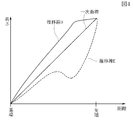
- FIG. 4 is a graph in which the horizontal axis is the distance from the proximal end to the distal end of the elastic arm, and the vertical axis is the height position of each portion of the elastic arm.
- FIG. 4 illustrates a linear curve connecting the height of the proximal end 12a and the height of the distal end 12b in a straight line.
- transition line D of the height in each portion of the three-dimensionally formed elastic arm 12 of the present embodiment shown in FIG. 2 is located above the linear curve in the graph as shown in FIG.
- the dotted transition line E shown in FIG. 4 is a comparative example shown in FIG. 8, and the transition line E is located below the linear curve in the graph.
- the width T2 is made substantially the same as the width T1 in order to reinforce the elastic arm 12 at the position of the width T2 where the large bending moment acts because the tip 12b is at the eccentric position.
- the transition line D of the height from the proximal end 12a to the distal end 12b is on a linear curve or above the linear curve.
- the mechanical strength can be strengthened against the elastic deformation of the elastic arm accompanied by the pressing movement of the spherical electrode of the electronic component, and the contact can be made less likely to be broken as compared with the prior art.
- Contour lines Y are shown on the surface of the elastic arm 12 in FIG. It can be seen that the contour lines Y are approximately equally spaced as compared to the comparative example of FIG.
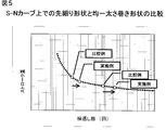
- FIG. 5 is a Goodman diagram (fatigue strength curve (SN curve)).
- the horizontal axis is the number (repeating number) when the contact is repeatedly depressed, and the horizontal axis is the displacement of the height of the contact (stroke amount).
- the horizontal axis is the number of repetitions when the contact is broken.
- the experiment was performed using the contact 10 of the embodiment shown in FIG. 1 and FIG. 2 and the contact of the comparative example shown in FIG. 7 and FIG. Then, using these contacts, push down the elastic arms of the contacts by a predetermined stroke amount and repeat the pressing process until the contacts break, and the number of repetitions and the stroke amount at that time are graphed. is there.
- the contactor 10 of the present embodiment can increase the number of repetitions as compared with the comparative example for substantially the same stroke, and can improve the mechanical strength.
- the width dimension of the elastic arm 12 may be gradually expanded from the position of the width dimension T1 to the position of the width dimension T2.
- the torsional stress acting on the elastic arm 12 at the position C of the width dimension T2 where the bending moment is large is more effective. Can be relaxed.
- the protrusion 14 is provided at the tip 12 b of the elastic arm 12.
- the protrusion 14 faces inward, that is, the drawing core O side.
- the position where the protrusion 14 is formed is not limited to the tip 12b, and the effect described above can be obtained as long as it is at least a portion of the elastic arm 12 sliding on the surface of the spherical electrode.
- providing the protrusion 14 in the vicinity of the front end ensures that the protrusion 14 cuts in the oxide film of the spherical electrode and conducts electricity, so that a more stable contact resistance can be secured.
- the electrode shape of the electronic component 40 is not limited to the spherical electrode 42 shown in FIG. In addition to the spherical shape, it has an electrode surface whose width dimension gradually decreases in the direction of the contact 10 as in a conical shape, and the electrode center is located in the space 15 of the elastic arm 12 When the electrode is pushed down, at least a part of the electrode is formed in a shape that can enter into the space 15 of the elastic arm 12, thereby sliding the oxide film on the electrode surface at the above-described tip. You can expect the effect of moving in and out.
- the electrodes may be flat. Although the effect of cutting in the above-mentioned oxide film can not be expected, the long life of the contact 10 can be realized by the improvement of the mechanical strength of the contact 10.
Landscapes
- Physics & Mathematics (AREA)
- General Physics & Mathematics (AREA)
- Geometry (AREA)
- Measuring Leads Or Probes (AREA)
Abstract
従来に比べて、機械的強度に優れた接触子及びその製造方法、ならびに接続装置を提供することを目的としている。弾性腕(12)は、平面で見たときに、先端(12b)が基端(12a)よりも巻きの内側に位置する巻回形状で形成されており、且つ前記基端(12a)から前記先端(12b)に向けて上方に立体成形されており、前記先端(12b)は前記弾性腕(12)の図芯Oから外れた位置に設けられており、平面視にて前記図芯Oと前記先端(12b)とを結ぶ基準線をX0としたとき、前記図芯Oから見て前記先端(12b)の外側に前記基準線X0を横断し横断位置にて幅寸法がT1で形成された1条の弾性腕と、前記先端(12b)から見て前記図芯Oの外側に前記基準線X0を横断し横断位置にて幅寸法がT2で形成された1条の弾性腕とを有し、前記幅寸法T2は前記幅寸法T1以上で形成されている。
Description
本発明は、巻回形成された導電性の弾性腕を備え、且つ前記弾性腕の基端から先端に向けて上方に立体成形された接触子及びその製造方法、ならびに接続装置に関する。
特許文献1には渦巻き形状の接触子が開示されており、弾性腕(渦巻き部)の幅が基端(根元)から先端に向うにしたがって徐々に狭くなっている。
図7は、比較例を示す接触子の平面図である。接触子1は、マウント部2と、前記マウント部2から延びる弾性腕3とで構成される。そして弾性腕3は、基端3aから先端3bにかけて徐々に幅寸法が小さくなっている。
図7に示すように前記先端3bは弾性腕3の図芯Oから外れた位置に設けられている。ここで「図芯」とは、弾性腕3の周縁からほぼ等距離にある点、又は、弾性腕3の略中心、あるいは、弾性腕3の略重心の位置として定義される。
また図7の平面視にて、弾性腕3の図芯Oと、先端3bとを結ぶ基準線をX0としたとき、前記図芯Oから見て前記先端1bの外側に前記基準線X0を横断し横断位置にて幅寸法がT3で形成された1条の弾性腕3と、前記先端3bから見て前記図芯Oの外側に前記基準線X0を横断し横断位置にて幅寸法がT4で形成された1条の弾性腕3とが設けられている。そして、幅寸法T4は幅寸法T3よりも小さい。
また図7に示すように前記先端3bの幅寸法の中心と、弾性腕3前記幅寸法T4の中心との間の距離L1は、前記先端3bの幅寸法の中心と、弾性腕3の前記幅寸法T3の中心との間の距離L2よりも大きい。
このため図7の平面形態から先端3bの位置を上方に押し上げ、前記弾性腕3を基端3aから先端3bに向って上方に立体成形したときに、曲げモーメントは、幅寸法T3の弾性腕3の位置よりも幅寸法T4の弾性腕3の位置で大きくなる。
しかしながら図7に示す比較例の形態では、前記幅寸法T4が前記幅寸法T3よりも小さいために上記のように弾性腕3を立体成形したときに前記幅寸法T4の位置でのねじり応力が強くなり、図8に示すように、弾性腕3は、幅寸法T4の位置A付近から先端3bにかけて急峻に傾くように立体成形されてしまう。また、幅寸法T4の位置A付近は、幅寸法T3の位置B付近に比べて下方に傾きやすくなる。なお、図7には弾性腕1の各部の等高線Yが弾性腕表面に図示されている。
図8に示すように弾性腕3が立体成形されると、電子部品の球状電極の押圧移動に伴って弾性腕3が弾性変形したとき、弾性腕3の前記幅寸法T4の位置A付近が機械的強度に弱く、しかも、幅寸法T4の位置A付近が下方に傾いているため、弾性腕1の弾性変形により前記幅寸法T4の位置A付近が接触子1を支持する基板に衝突する等して損傷を受けやすい(最悪、折れてしまう)。
特開2002-175859号公報
そこで本発明は、上記従来の課題を解決するものであり、従来に比べて、機械的強度に優れた接触子及びその製造方法、ならびに接続装置を提供することを目的としている。
本発明は、電子部品の電極と電気的に接続される導電性の弾性腕を備える接触子において、
前記弾性腕は、平面で見たときに、先端が基端よりも巻きの内側に位置する巻回形状で形成されており、且つ前記基端から前記先端に向けて上方に立体成形されており、
前記先端は前記弾性腕の図芯から外れた位置に設けられており、
平面視にて前記図芯と前記先端とを結ぶ基準線をX0としたとき、前記図芯から見て前記先端の外側に前記基準線X0を横断し横断位置にて幅寸法がT1で形成された1条の弾性腕と、前記先端から見て前記図芯の外側に前記基準線X0を横断し横断位置にて幅寸法がT2で形成された1条の弾性腕とを有し、
前記幅寸法T2は前記幅寸法T1以上で形成されていることを特徴とするものである。
前記弾性腕は、平面で見たときに、先端が基端よりも巻きの内側に位置する巻回形状で形成されており、且つ前記基端から前記先端に向けて上方に立体成形されており、
前記先端は前記弾性腕の図芯から外れた位置に設けられており、
平面視にて前記図芯と前記先端とを結ぶ基準線をX0としたとき、前記図芯から見て前記先端の外側に前記基準線X0を横断し横断位置にて幅寸法がT1で形成された1条の弾性腕と、前記先端から見て前記図芯の外側に前記基準線X0を横断し横断位置にて幅寸法がT2で形成された1条の弾性腕とを有し、
前記幅寸法T2は前記幅寸法T1以上で形成されていることを特徴とするものである。
上記のように、本発明は、前記弾性腕の先端が前記弾性腕の図芯から外れた位置にある。ここで「図芯」とは、弾性腕の周縁からほぼ等距離にある点、あるいは、弾性腕3の略中心、又はほぼ重心の位置として定義される。
そして、本発明では、平面視にて前記図芯と前記先端とを結ぶ基準線をX0としたとき、前記図芯から見て前記先端の外側に前記基準線X0を横断し横断位置にて幅寸法がT1で形成された1条の弾性腕と、前記先端から見て前記図芯の外側に前記基準線X0を横断し横断位置にて幅寸法がT2で形成された1条の弾性腕とを有し、前記幅寸法T2が前記幅寸法T1以上で形成されている。
本発明では、図1に示すように例えば、弾性腕12の基端12aから先端12bにかけて略一定の幅寸法で形成する。図1に示すように、弾性腕12の先端12bは図芯Oから外れた位置にある。また図1に示すように、弾性腕12の図芯Oと、先端12bとを結ぶ基準線をX0としたとき、前記図芯Oから見て前記先端12bの外側に前記基準線X0を横断し横断位置にて幅寸法T1で形成された1条の弾性腕と、前記先端12bから見て前記図芯Oの外側に前記基準線X0を横断し横断位置にて幅寸法がT2で形成された1条の弾性腕とが設けられている。
また図1に示すように前記先端12bの幅寸法の中心と、弾性腕12の前記幅寸法T2の中心との間の距離L1は、前記先端12bの幅寸法の中心と、弾性腕12の前記幅寸法T1の中心との間の距離L2よりも大きい。
このため図1の平面形態から先端12bの位置を上方に押し上げて、弾性腕12を基端12aから先端12bに向って上方に立体成形したときに、曲げモーメントは、幅寸法T1の弾性腕12の位置よりも幅寸法T2の弾性腕12の位置で大きくなるが、図7に示す比較例と異なり、図1の本発明では、前記幅寸法T2を前記幅寸法T1と略同一とした。この結果、図7に示す比較例に比べて、先端12bを上方に押し上げて弾性腕12を立体成形したときに前記幅寸法T2の位置C付近(図2参照)に作用するねじり応力を分散でき(小さくでき)、幅寸法T2の位置Cを適切に上方に持上げることが出来る。よって、図7,図8の比較例の形態に比べて電子部品の電極の押圧移動に伴う弾性腕の弾性変形に対して機械的強度を強くでき、従来に比べて折れにくい接触子に出来る。
本発明では、前記幅寸法T1(図1参照)の位置から前記幅寸法T2の位置にかけて徐々に前記弾性腕の幅寸法が広がる形態としてもよい。
また、本発明は、電子部品の電極と電気的に接続される導電性の弾性腕を備える接触子を有する接続装置において、
前記接触子は上記に記載された構成で形成されており、
平面視にて、前記弾性腕の前記先端は、電極中心から外れた位置にあることを特徴とするものである。これにより、電子部品の電極が球状や円錐形状等であるとき、前記電極の押圧移動に伴って前記弾性腕の先端が電極表面を摺動するように弾性腕が弾性変形する。この結果、軽い荷重で、電極表面の酸化皮膜を切り込んで導通し安定した接触抵抗を確保できる。
前記接触子は上記に記載された構成で形成されており、
平面視にて、前記弾性腕の前記先端は、電極中心から外れた位置にあることを特徴とするものである。これにより、電子部品の電極が球状や円錐形状等であるとき、前記電極の押圧移動に伴って前記弾性腕の先端が電極表面を摺動するように弾性腕が弾性変形する。この結果、軽い荷重で、電極表面の酸化皮膜を切り込んで導通し安定した接触抵抗を確保できる。
また本発明では、前記弾性腕には前記電子部品の押圧移動に伴って電極表面を摺動する突起部が形成されていることが好ましい。前記突起部は前記弾性腕の先端付近に形成されていることがより好ましい。前記突起部を設けることで、電子部品の電極の押圧移動に伴い突起部が球状あるいは円錐形状等の電極表面を摺動して切り込むことにより、より効果的に安定した接触抵抗を確保できる。
本発明は、球状電極を有する電子部品に電気的に接続される導電性の弾性腕を備える接触子において、
前記弾性腕は、平面で見たときに、先端が基端よりも巻きの内側に位置する巻回形状で形成されており、且つ前記基端から前記先端に向けて上方に立体成形されており、
前記先端は前記弾性腕の図芯から外れた位置に設けられており、
前記基端の位置から前記先端の位置までの距離を横軸に、前記基端から前記先端の高さ位置を縦軸としたグラフ上に、前記基端の高さ位置から前記先端の高さ位置に直線状に引いた一次曲線に対して、前記基端から前記先端までの高さの推移線が前記一次曲線上、あるいは前記一次曲線よりもグラフ上方に位置しており、
前記先端には突起部が図芯方向に向けて形成され、
前記電子部品の押圧移動に伴って前記球状電極の表面を摺動し、前記突起部により前記球状電極の表面に形成された皮膜に対し切込みを入れ電気的接続を行うことを特徴とするものである。
前記弾性腕は、平面で見たときに、先端が基端よりも巻きの内側に位置する巻回形状で形成されており、且つ前記基端から前記先端に向けて上方に立体成形されており、
前記先端は前記弾性腕の図芯から外れた位置に設けられており、
前記基端の位置から前記先端の位置までの距離を横軸に、前記基端から前記先端の高さ位置を縦軸としたグラフ上に、前記基端の高さ位置から前記先端の高さ位置に直線状に引いた一次曲線に対して、前記基端から前記先端までの高さの推移線が前記一次曲線上、あるいは前記一次曲線よりもグラフ上方に位置しており、
前記先端には突起部が図芯方向に向けて形成され、
前記電子部品の押圧移動に伴って前記球状電極の表面を摺動し、前記突起部により前記球状電極の表面に形成された皮膜に対し切込みを入れ電気的接続を行うことを特徴とするものである。
上記において、前記弾性腕は、前記基端から前記先端にかけて略一定の幅寸法で形成されていることが好ましい。
また、本発明は、電子部品の電極と電気的に接続される導電性の弾性腕を備える接触子の製造方法において、
前記弾性腕を、平面内に形成し、このとき、先端が基端よりも巻きの内側に位置する巻回形状で形成し、前記先端を前記弾性腕の図芯から外れた位置に設け、
さらに、平面視にて前記図芯と前記先端とを結ぶ基準線をX0としたとき、前記図芯から見て前記先端の外側に前記基準線X0を横断し横断位置にて幅寸法がT1で形成された1条の弾性腕と、前記先端から見て前記図芯の外側に前記基準線X0を横断し横断位置にて幅寸法がT1以上のT2で形成された1条の弾性腕とを有して形成し、
続いて、前記先端を上方に押し上げて、前記弾性腕を基端から先端に向けて上方に立ち上がるように立体成形することを特徴とするものである。
前記弾性腕を、平面内に形成し、このとき、先端が基端よりも巻きの内側に位置する巻回形状で形成し、前記先端を前記弾性腕の図芯から外れた位置に設け、
さらに、平面視にて前記図芯と前記先端とを結ぶ基準線をX0としたとき、前記図芯から見て前記先端の外側に前記基準線X0を横断し横断位置にて幅寸法がT1で形成された1条の弾性腕と、前記先端から見て前記図芯の外側に前記基準線X0を横断し横断位置にて幅寸法がT1以上のT2で形成された1条の弾性腕とを有して形成し、
続いて、前記先端を上方に押し上げて、前記弾性腕を基端から先端に向けて上方に立ち上がるように立体成形することを特徴とするものである。
これにより図7に示す比較例のように、基端から先端にかけて幅寸法が徐々に小さくなる形態に比べて、先端を上方に押し上げて弾性腕を立体成形したときに幅寸法T2の位置付近に作用するねじり応力を分散でき(小さくでき)、弾性腕の幅寸法T2の位置を適切に上方に持上げることが出来る。
本発明の接触子及び、前記接触子を備えた接続装置によれば、優れた機械的強度を得ることが出来る。さらに電子部品の球状電極等に対して安定した接触抵抗を確保できる。
図1は本発明の実施の形態の接触子10を示す平面図、図2は接触子10の側面図である。
接触子10は、エッチング法またはメッキ法により形成されるものである。エッチング法では、薄い板状の銅膜をエッチングすることにより図1に示す形状が形成され、さらにその表面に、ニッケルやニッケル-リンなどの補強メッキが施される。または、銅とニッケルとの積層体や、銅とニッケル-リンとの積層体で形成することもできる。この構造では、主にニッケルまたはニッケル-リンが弾性機能を発揮し、銅が比抵抗を低下させるように機能する。
または、接触子10を、銅層をメッキすることで形成でき、あるいは銅とニッケルとを連続メッキで積層して成膜し、または銅とニッケル-リンを連続メッキで積層して成膜することで形成することができる。
図1に示すように接触子10は、所定の膜厚で平面的な形状のマウント部11と、このマウント部11から延び出る弾性腕12とが一体に形成されている。弾性腕12は、前記マウント部11との境界部が基端12aであり、先端12bは巻回パターンの内側に位置している。図1には、弾性腕12の腕中心線をφで示している。この腕中心線φは、弾性腕3の各位置において弾性腕3の幅寸法を二分する点を結んだ連続線であり、この腕中心線φも螺旋形状である。
図1に示すOは、弾性腕12の図芯である。本実施形態では、前記図芯Oは、弾性腕12の周縁からほぼ等距離にある点、あるいは、弾性腕3の略中心、又は、弾性腕3の略重心の位置として定義される。なお、前記図芯Oは、電子部品の電極中心と一致していてもよいし、一致していなくてもよい。
図1に示すように、弾性腕12の先端12bは図芯Oから外れた位置に設けられ、且つ、前記電極中心からも外れた位置にある。図1のように弾性腕12の略中央には空間15が設けられ、この空間15内に図芯O及び電極中心が位置する。
図3には、接触子10を備える接続装置20が図示されている。接続装置20は、基台21を有している。基台21の平面形状は例えば四角形状であり、基台21の4辺のそれぞれにはほぼ垂直に立ち上がる側壁部21aが形成されている。4辺の側壁部21aで囲まれた領域は凹部であり、その底部21bの上面が支持面22である。支持面22の上には、接続シート25が設置されている。接続シート25は、例えば、可撓性の基材シート26の表面に複数の接触子10が設けられた構成である。
図3に示すように、接続装置20には、電子部品40が設置される。電子部品40は、ICパッケージなどであり、ICベアチップなどの各種電子素子が本体部41内に密閉されている。本体部41の底面41aには、複数の球状電極42が設けられており、それぞれの球状電極42が本体部41内の回路に導通している。
図1に示すように、電子部品40が、基台10の凹部内に装着される。このとき、電子部品40は、本体部41の底面41aに設けられた個々の球状電極42が接触子10の上に設置されるように位置決めされる。基台21の上には図示しない押圧用の蓋体が設けられており、この蓋体を基台21上に被せると、この蓋体により電子部品40が矢印F方向へ押圧される。この押圧力により、それぞれの球状電極42が弾性腕12に押し付けられ、弾性腕12が押しつぶされて、球状電極42と弾性腕12とが個別に導通させられる。
本実施形態における接触子10の弾性腕12は、図2に示すように基端12aから先端12bに向って上方に立体成形されている。立体成形は、図1に示す平面内の接触子10を形成した後、先端12b付近に治具(ピン)の押し上げ面を当接し、前記先端12b付近を前記治具にて押し上げることで達成できる。また先端12bを押し上げた状態で所定時間加熱し内部応力を緩和することが好適である。
また、例えば、円錐形状の治具を使うことで、弾性腕12の幅や厚さに関係なく所望の形状を得ることができる。
本実施形態の接触子10の特徴的構成について説明する。図1に示すように弾性腕12の先端12bは、前記弾性腕12の図芯Oから外れた位置にある。また弾性腕12の先端12bは、図3に示す接続装置20において、球状電極42の電極中心から外れた位置にある。これにより、図3に示す球状電極42の押圧移動に伴って前記弾性腕12の先端12bが球状電極表面を摺動するように弾性腕12が弾性変形する。図6(a)は、摺動しない接点の模式図、図6(b)は摺動接点の模式図、である。図6(a)のように電極中心下方向に直交して接点がある場合、電極が下方に押されても接点も下方に押されるだけで、接点は電極表面を摺動しない。一方、図6(b)のように、電極中心下方向に接点が直交していない場合、接点の長さ方向に分力が作用して、電極表面に対して接点が摺動する。本実施形態は、図6(b)に示す摺動接点と同様であり、この結果、軽い荷重で、球状電極表面を摺動し、このとき、酸化皮膜を切り込んで導通し安定した接触抵抗を確保できる。
さらに本実施形態では、図1に示すように、平面視にて前記図芯Oと前記先端12bとを結ぶ基準線をX0としたとき、前記図芯Oから見て前記先端12bの外側に前記基準線X0を横断し横断位置にて幅寸法がT1で形成された1条の弾性腕と、前記先端12bから見て前記図芯Oの外側に前記基準線X0を横断し横断位置にて幅寸法がT2で形成された1条の弾性腕とを有し、前記幅寸法T2が前記幅寸法T1以上で形成されている。
図1に示す実施形態では、弾性腕12の基端12aから先端12bにかけて略一定の幅寸法で形成されている。よって図1に示す幅寸法T1と幅寸法T2は略同一である。
図1に示すように弾性腕12が巻回形成され、その先端12bが図芯Oから外れた位置にある形態では、先端12bの幅中心から、弾性腕12の各部分の幅中心までの距離の増減傾向が、途中で変化してしまう。図1に示すように、先端12bの幅中心O1から基端12aまでの距離は大きく、前記基端12aから先端12bに向けて先端12bの幅中心O1との距離は徐々に小さくなるが、幅寸法T1付近を境にして先端12bの幅中心O1との距離は、大きくなっていき、さらに幅寸法T2付近を境にして先端12bの幅中心O1との距離は再び、小さくなっていく。
曲げモーメントについて考察すると、先端12bの幅中心O1からの距離が大きいほど曲げモーメントは大きくなるから、基準線X0上に位置する幅寸法T1の位置と幅寸法T2の位置を比較すると、幅寸法T2の位置での曲げモーメントは幅寸法T1の位置での曲げモーメントに比べて大きくなる。特に、幅寸法T2の位置では、先端12bの幅中心からの距離が基端12a付近を除けば、ほぼ最大に大きいため、曲げモーメントが非常に大きくなっている。
そこで図1に示す実施形態では、弾性腕12の基端12aから先端12bにかけて幅寸法を略一定で形成した。これにより、前記幅寸法T2と幅寸法T1は略同一になる。この結果、図7に示す比較例のように、基端から先端にかけて幅寸法が徐々に小さくなる形態に比べて、先端12bを上方に押し上げて弾性腕12を立体成形したときに幅寸法T2の位置C付近(図2参照)に作用するねじり応力を分散でき(小さくでき)、幅寸法T2の位置Cを適切に上方に持上げることが出来る。
図4は、横軸を弾性腕の基端から先端までの距離とし、縦軸を弾性腕の各部分の高さ位置としたグラフである。図4には、基端12aの高さと、先端12bの高さとを直線で結んだ一次曲線が図示されている。
図2に示す本実施形態の立体成形された弾性腕12の各部分における高さの推移線Dは、図4に示すように一次曲線よりもグラフ上方に位置している。一方、図4に示す点線の推移線Eは、図8に示す比較例であり、前記推移線Eは前記一次曲線よりもグラフ下方に位置している。
本実施形態は、先端12bが偏心位置にあるために大きい曲げモーメントが作用する幅寸法T2の位置の弾性腕12を補強すべく前記幅寸法T2を幅寸法T1と略同一としたのである。
本実施形態では、図4のグラフにおいて、基端12aから先端12bの高さの推移線Dが一次曲線上、あるいは前記一次曲線よりもグラフ上方にあることが好適であり、これにより、図8の比較例の形態に比べて電子部品の球状電極の押圧移動に伴う弾性腕の弾性変形に対して機械的強度を強くでき、従来に比べて折れにくい接触子に出来る。なお図1には弾性腕12の表面に等高線Yを図示した。図7の比較例に比べて等高線Yがほぼ等間隔になっていることがわかる。
図5はグッドマン線図(疲労強度曲線(S-N曲線))である。横軸を、接触子に対して繰り返し押し下げたときの数(繰り返し数)、横軸を接触子の高さの変位量(ストローク量)とした。横軸は接触子が折れたときの繰り返し数である。
実験は、図1,図2に示す実施形態の接触子10と、図7,図8に示す比較例の接触子を用いて行った。そして、これらの接触子を用い、予め決められたストローク量で接触子の弾性腕を押し下げ、押し下げ工程を接触子が折れるまで繰り返し行い、そのときの繰り返し数とストローク量とをグラフにしたものである。
図5に示すように略同一ストロークに対し本実施形態の接触子10のほうが比較例に対して繰り返し数を多くでき、機械的強度を向上させることができるとわかった。
また、本実施形態では、前記幅寸法T1の位置から前記幅寸法T2の位置にかけて徐々に前記弾性腕12の幅寸法が広がっている形態にすることも可能である。特に、このような形態にすれば、先端12bを上方に押し上げて弾性腕12を立体成形するときに、曲げモーメントが大きい幅寸法T2の位置Cでの弾性腕12に作用するねじり応力をより効果的に緩和できる。
図1に示す実施形態では、弾性腕12の先端12bに突起部14が設けられている。突起部14は内側、すなわち図芯O側を向いている。このような突起部14を設けたことで、電子部品40の球状電極42の押圧移動に伴い突起部14が球状電極表面を摺動して切り込み、より効果的に安定した接触抵抗を確保できる。
突起部14の形成位置は先端12bに限定せず、少なくとも球状電極の表面に摺動する弾性腕12の部分であれば上記した効果を得ることができる。ただし突起部14を先端付近に設けることが、突起部14が確実に球状電極の酸化皮膜を切り込んで導通するため、より効果的に安定した接触抵抗を確保できる。
電子部品40の電極形状は図3に示す球状電極42に限定されない。球状以外に円錐形状等のように接触子10の方向に向うにしたがって徐々に幅寸法が小さくなる電極表面を備え、電極中心が弾性腕12の空間15内に位置し、さらに、接続装置にて電極が押し下げられると、前記電極の少なくとも一部が、弾性腕12の空間15内に入り込むことが可能な形状で形成されており、これにより、上記した先端にて、電極表面の酸化皮膜を摺動して切り込む効果を期待できる。
また電極は平板状であってもよい。上記の酸化皮膜を切り込む効果は期待できないが接触子10の機械的強度の向上により、接触子10の長寿命を実現できる。
10 接触子
11 マウント部
12 弾性腕
12a (弾性腕の)基端
12b (弾性腕の)先端
14 突起部
15 空間
20 接続装置
21 基台
25 接続シート
40 電子部品
42 球状電極
11 マウント部
12 弾性腕
12a (弾性腕の)基端
12b (弾性腕の)先端
14 突起部
15 空間
20 接続装置
21 基台
25 接続シート
40 電子部品
42 球状電極
Claims (9)
- 電子部品の電極と電気的に接続される導電性の弾性腕を備える接触子において、
前記弾性腕は、平面で見たときに、先端が基端よりも巻きの内側に位置する巻回形状で形成されており、且つ前記基端から前記先端に向けて上方に立体成形されており、
前記先端は前記弾性腕の図芯から外れた位置に設けられており、
平面視にて前記図芯と前記先端とを結ぶ基準線をX0としたとき、前記図芯から見て前記先端の外側に前記基準線X0を横断し横断位置にて幅寸法がT1で形成された1条の弾性腕と、前記先端から見て前記図芯の外側に前記基準線X0を横断し横断位置にて幅寸法がT2で形成された1条の弾性腕とを有し、
前記幅寸法T2は前記幅寸法T1以上で形成されていることを特徴とする接触子。 - 前記弾性腕は、前記基端から前記先端にかけて略一定の幅寸法で形成されている請求項1記載の接触子。
- 前記幅寸法T1の位置から前記幅寸法T2の位置にかけて徐々に前記弾性腕の幅寸法が広がっている請求項1記載の接触子。
- 電子部品の電極と電気的に接続される導電性の弾性腕を備える接触子を有する接続装置において、
前記接触子は請求項1ないし3のいずれか1項に記載された構成で形成されており、
平面視にて、前記弾性腕の前記先端は、電極中心から外れた位置にあることを特徴とする接続装置。 - 前記弾性腕には前記電子部品の押圧移動に伴って電極表面を摺動する突起部が形成されている請求項4記載の接続装置。
- 前記突起部は前記弾性腕の先端付近に形成されている請求項5記載の接続装置。
- 球状電極を有する電子部品に電気的に接続される導電性の弾性腕を備える接触子において、
前記弾性腕は、平面で見たときに、先端が基端よりも巻きの内側に位置する巻回形状で形成されており、且つ前記基端から前記先端に向けて上方に立体成形されており、
前記先端は前記弾性腕の図芯から外れた位置に設けられており、
前記基端の位置から前記先端の位置までの距離を横軸に、前記基端から前記先端の高さ位置を縦軸としたグラフ上に、前記基端の高さ位置から前記先端の高さ位置に直線状に引いた一次曲線に対して、前記基端から前記先端までの高さの推移線が前記一次曲線上、あるいは前記一次曲線よりもグラフ上方に位置しており、
前記先端には突起部が図芯方向に向けて形成され、
前記電子部品の押圧移動に伴って前記球状電極の表面を摺動し、前記突起部により前記球状電極の表面に形成された皮膜に対し切込みを入れ電気的接続を行うことを特徴とする接触子。 - 前記弾性腕は、前記基端から前記先端にかけて略一定の幅寸法で形成されている請求項7記載の接触子。
- 電子部品の電極と電気的に接続される導電性の弾性腕を備える接触子の製造方法において、
前記弾性腕を、平面内に形成し、このとき、先端が基端よりも巻きの内側に位置する巻回形状で形成し、前記先端を前記弾性腕の図芯から外れた位置に設け、
さらに、平面視にて前記図芯と前記先端とを結ぶ基準線をX0としたとき、前記図芯から見て前記先端の外側に前記基準線X0を横断し横断位置にて幅寸法がT1で形成された1条の弾性腕と、前記先端から見て前記図芯の外側に前記基準線X0を横断し横断位置にて幅寸法がT1以上のT2で形成された1条の弾性腕とを有して形成し、
続いて、前記先端を上方に押し上げて、前記弾性腕を基端から先端に向けて上方に立ち上がるように立体成形することを特徴とする接触子の製造方法。
Applications Claiming Priority (2)
| Application Number | Priority Date | Filing Date | Title |
|---|---|---|---|
| JP2009006771 | 2009-01-15 | ||
| JP2009-006771 | 2009-01-15 |
Publications (1)
| Publication Number | Publication Date |
|---|---|
| WO2010082576A1 true WO2010082576A1 (ja) | 2010-07-22 |
Family
ID=42339830
Family Applications (1)
| Application Number | Title | Priority Date | Filing Date |
|---|---|---|---|
| PCT/JP2010/050261 Ceased WO2010082576A1 (ja) | 2009-01-15 | 2010-01-13 | 接触子及びその製造方法、ならびに前記接触子を備えた接続装置 |
Country Status (2)
| Country | Link |
|---|---|
| TW (1) | TW201042845A (ja) |
| WO (1) | WO2010082576A1 (ja) |
Citations (4)
| Publication number | Priority date | Publication date | Assignee | Title |
|---|---|---|---|---|
| JP2005129428A (ja) * | 2003-10-27 | 2005-05-19 | Sumitomo Electric Ind Ltd | 竹の子状コンタクトの製造方法、その方法により製造されたコンタクトおよびそのコンタクトを備える検査装置または電子機器 |
| JP2006269148A (ja) * | 2005-03-23 | 2006-10-05 | Alps Electric Co Ltd | スパイラル接触子 |
| JP2006269149A (ja) * | 2005-03-23 | 2006-10-05 | Alps Electric Co Ltd | 接点部材及びその製造方法 |
| JP2008249466A (ja) * | 2007-03-30 | 2008-10-16 | Advanced Systems Japan Inc | 凸形ケルビン・スパイラルコンタクタ及びその製造方法 |
-
2010
- 2010-01-06 TW TW99100194A patent/TW201042845A/zh unknown
- 2010-01-13 WO PCT/JP2010/050261 patent/WO2010082576A1/ja not_active Ceased
Patent Citations (4)
| Publication number | Priority date | Publication date | Assignee | Title |
|---|---|---|---|---|
| JP2005129428A (ja) * | 2003-10-27 | 2005-05-19 | Sumitomo Electric Ind Ltd | 竹の子状コンタクトの製造方法、その方法により製造されたコンタクトおよびそのコンタクトを備える検査装置または電子機器 |
| JP2006269148A (ja) * | 2005-03-23 | 2006-10-05 | Alps Electric Co Ltd | スパイラル接触子 |
| JP2006269149A (ja) * | 2005-03-23 | 2006-10-05 | Alps Electric Co Ltd | 接点部材及びその製造方法 |
| JP2008249466A (ja) * | 2007-03-30 | 2008-10-16 | Advanced Systems Japan Inc | 凸形ケルビン・スパイラルコンタクタ及びその製造方法 |
Also Published As
| Publication number | Publication date |
|---|---|
| TW201042845A (en) | 2010-12-01 |
Similar Documents
| Publication | Publication Date | Title |
|---|---|---|
| US7891983B2 (en) | Contact and IC socket using the same | |
| CN109361094B (zh) | 电连接器 | |
| JP6269337B2 (ja) | プローブピン、および、これを用いた電子デバイス | |
| US8816219B2 (en) | Metal strip assembly for EMI shield case, EMI shield case including the same, and fabrication method of the case | |
| CN107565235A (zh) | 电连接器 | |
| JP2008198597A (ja) | 接触バネを有するパワー半導体モジュール | |
| JP2013008467A (ja) | コンタクトおよびソケット | |
| WO2007138952A1 (ja) | ソケット用コンタクト端子及び半導体装置 | |
| JP2013007700A (ja) | 電気的接触子 | |
| JP6176848B2 (ja) | 雌コネクタ | |
| JP2009128211A (ja) | プローブピン | |
| JP6247517B2 (ja) | 薄型コネクタ | |
| JP6532877B2 (ja) | バッテリコネクタおよびその製造方法 | |
| US20100041254A1 (en) | Socket for burn-in tests | |
| KR101870842B1 (ko) | 탄성 전기접촉단자 | |
| WO2010082576A1 (ja) | 接触子及びその製造方法、ならびに前記接触子を備えた接続装置 | |
| US8684775B2 (en) | Electrical connector and terminal thereof | |
| JP2007518242A (ja) | インターポーザ組立部品 | |
| JP2006269148A (ja) | スパイラル接触子 | |
| US20100255733A1 (en) | Electrical contact having an upper contact with a thickened base portion | |
| JP5644909B2 (ja) | ブラシ | |
| JP2009193883A (ja) | 接続端子、コネクタおよび半導体パッケージ | |
| JP2005292019A (ja) | プローブ | |
| JP2014044821A (ja) | ハウジングレスコネクタ | |
| KR20160110717A (ko) | 탄성 시그널 핀 |
Legal Events
| Date | Code | Title | Description |
|---|---|---|---|
| 121 | Ep: the epo has been informed by wipo that ep was designated in this application |
Ref document number: 10731245 Country of ref document: EP Kind code of ref document: A1 |
|
| NENP | Non-entry into the national phase |
Ref country code: DE |
|
| 122 | Ep: pct application non-entry in european phase |
Ref document number: 10731245 Country of ref document: EP Kind code of ref document: A1 |
|
| NENP | Non-entry into the national phase |
Ref country code: JP |