WO2010082401A1 - 発光装置 - Google Patents
発光装置 Download PDFInfo
- Publication number
- WO2010082401A1 WO2010082401A1 PCT/JP2009/070014 JP2009070014W WO2010082401A1 WO 2010082401 A1 WO2010082401 A1 WO 2010082401A1 JP 2009070014 W JP2009070014 W JP 2009070014W WO 2010082401 A1 WO2010082401 A1 WO 2010082401A1
- Authority
- WO
- WIPO (PCT)
- Prior art keywords
- electrode
- frame
- light emitting
- semiconductor laser
- emitting device
- Prior art date
- Legal status (The legal status is an assumption and is not a legal conclusion. Google has not performed a legal analysis and makes no representation as to the accuracy of the status listed.)
- Ceased
Links
Images


Classifications
-
- H—ELECTRICITY
- H01—ELECTRIC ELEMENTS
- H01S—DEVICES USING THE PROCESS OF LIGHT AMPLIFICATION BY STIMULATED EMISSION OF RADIATION [LASER] TO AMPLIFY OR GENERATE LIGHT; DEVICES USING STIMULATED EMISSION OF ELECTROMAGNETIC RADIATION IN WAVE RANGES OTHER THAN OPTICAL
- H01S5/00—Semiconductor lasers
- H01S5/40—Arrangement of two or more semiconductor lasers, not provided for in groups H01S5/02 - H01S5/30
- H01S5/4025—Array arrangements, e.g. constituted by discrete laser diodes or laser bar
- H01S5/4031—Edge-emitting structures
-
- H—ELECTRICITY
- H01—ELECTRIC ELEMENTS
- H01S—DEVICES USING THE PROCESS OF LIGHT AMPLIFICATION BY STIMULATED EMISSION OF RADIATION [LASER] TO AMPLIFY OR GENERATE LIGHT; DEVICES USING STIMULATED EMISSION OF ELECTROMAGNETIC RADIATION IN WAVE RANGES OTHER THAN OPTICAL
- H01S5/00—Semiconductor lasers
- H01S5/02—Structural details or components not essential to laser action
- H01S5/022—Mountings; Housings
- H01S5/023—Mount members, e.g. sub-mount members
- H01S5/0231—Stems
-
- H—ELECTRICITY
- H01—ELECTRIC ELEMENTS
- H01S—DEVICES USING THE PROCESS OF LIGHT AMPLIFICATION BY STIMULATED EMISSION OF RADIATION [LASER] TO AMPLIFY OR GENERATE LIGHT; DEVICES USING STIMULATED EMISSION OF ELECTROMAGNETIC RADIATION IN WAVE RANGES OTHER THAN OPTICAL
- H01S5/00—Semiconductor lasers
- H01S5/02—Structural details or components not essential to laser action
- H01S5/022—Mountings; Housings
- H01S5/023—Mount members, e.g. sub-mount members
- H01S5/0232—Lead-frames
-
- H—ELECTRICITY
- H01—ELECTRIC ELEMENTS
- H01S—DEVICES USING THE PROCESS OF LIGHT AMPLIFICATION BY STIMULATED EMISSION OF RADIATION [LASER] TO AMPLIFY OR GENERATE LIGHT; DEVICES USING STIMULATED EMISSION OF ELECTROMAGNETIC RADIATION IN WAVE RANGES OTHER THAN OPTICAL
- H01S5/00—Semiconductor lasers
- H01S5/02—Structural details or components not essential to laser action
- H01S5/022—Mountings; Housings
- H01S5/0233—Mounting configuration of laser chips
- H01S5/0234—Up-side down mountings, e.g. Flip-chip, epi-side down mountings or junction down mountings
-
- H—ELECTRICITY
- H01—ELECTRIC ELEMENTS
- H01S—DEVICES USING THE PROCESS OF LIGHT AMPLIFICATION BY STIMULATED EMISSION OF RADIATION [LASER] TO AMPLIFY OR GENERATE LIGHT; DEVICES USING STIMULATED EMISSION OF ELECTROMAGNETIC RADIATION IN WAVE RANGES OTHER THAN OPTICAL
- H01S5/00—Semiconductor lasers
- H01S5/02—Structural details or components not essential to laser action
- H01S5/022—Mountings; Housings
- H01S5/0233—Mounting configuration of laser chips
- H01S5/02345—Wire-bonding
-
- H—ELECTRICITY
- H01—ELECTRIC ELEMENTS
- H01S—DEVICES USING THE PROCESS OF LIGHT AMPLIFICATION BY STIMULATED EMISSION OF RADIATION [LASER] TO AMPLIFY OR GENERATE LIGHT; DEVICES USING STIMULATED EMISSION OF ELECTROMAGNETIC RADIATION IN WAVE RANGES OTHER THAN OPTICAL
- H01S5/00—Semiconductor lasers
- H01S5/02—Structural details or components not essential to laser action
- H01S5/026—Monolithically integrated components, e.g. waveguides, monitoring photo-detectors, drivers
-
- H—ELECTRICITY
- H01—ELECTRIC ELEMENTS
- H01S—DEVICES USING THE PROCESS OF LIGHT AMPLIFICATION BY STIMULATED EMISSION OF RADIATION [LASER] TO AMPLIFY OR GENERATE LIGHT; DEVICES USING STIMULATED EMISSION OF ELECTROMAGNETIC RADIATION IN WAVE RANGES OTHER THAN OPTICAL
- H01S5/00—Semiconductor lasers
- H01S5/40—Arrangement of two or more semiconductor lasers, not provided for in groups H01S5/02 - H01S5/30
- H01S5/4025—Array arrangements, e.g. constituted by discrete laser diodes or laser bar
- H01S5/4087—Array arrangements, e.g. constituted by discrete laser diodes or laser bar emitting more than one wavelength
-
- H—ELECTRICITY
- H10—SEMICONDUCTOR DEVICES; ELECTRIC SOLID-STATE DEVICES NOT OTHERWISE PROVIDED FOR
- H10W—GENERIC PACKAGES, INTERCONNECTIONS, CONNECTORS OR OTHER CONSTRUCTIONAL DETAILS OF DEVICES COVERED BY CLASS H10
- H10W90/00—Package configurations
- H10W90/701—Package configurations characterised by the relative positions of pads or connectors relative to package parts
- H10W90/751—Package configurations characterised by the relative positions of pads or connectors relative to package parts of bond wires
- H10W90/756—Package configurations characterised by the relative positions of pads or connectors relative to package parts of bond wires between a chip and a stacked lead frame, conducting package substrate or heat sink
Definitions
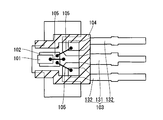
- the present invention relates to a light emitting device including a frame on which a light emitting element is mounted.
- a semiconductor laser element 101 is used as a light emitting element, and the semiconductor laser element 101 is attached to a submount 102 by a junction down method.
- the semiconductor laser element 101 is a two-wavelength laser element, and the p-side electrode is divided into two and the n-side electrode is common. Further, the p-side electrode and the n-side electrode of the semiconductor laser element 101 are formed so as to sandwich the semiconductor layer (light emitting portion) and the substrate.
- the p-side electrode of the semiconductor laser element 101 is fixed to the submount 102 and is electrically connected.
- the semiconductor laser device 101 attached to the submount 102 is mounted on a three-terminal frame 103.
- the frame 103 includes one main frame 131 and two sub frames 132 that are electrically insulated from each other, and has a structure in which they are fixed to each other by a resin 104.
- the submount 102 is fixed to the main frame 131 of the main frame 131 and the subframe 132.
- the n-side electrode of the semiconductor laser element 101 and the main frame 131 are electrically connected via the bonding wire 105.
- the submount 102 is electrically connected to the subframe 132 via the bonding wire 105. That is, the p-side electrode of the semiconductor laser element 101 and the sub frame 132 are electrically connected.
- the semiconductor laser element 101 and the frame 103 are electrically connected via the bonding wire 105.
- the bonding wire 105 comes into contact with the outside, the bonding wire 105 is disconnected. There is a fear. That is, the conventional light emitting device that requires the bonding wire 105 has a disadvantage that a connection failure is likely to occur between the semiconductor laser element 101 and the frame 103.
- the present invention has been made to solve the above-described problems, and an object thereof is to provide a light-emitting device that can eliminate the need for a bonding wire.
- a light-emitting device includes at least a first electrode and a second electrode, and a light-emitting element having a light-emitting portion provided between the first electrode and the second electrode.
- the first electrode of the light emitting element is electrically connected and has a base having a fixed electrode surface on the predetermined surface side, an element mounting portion on which the light emitting element is mounted, and an element mounting A first frame in which the second electrode of the light emitting element is electrically connected to the part, and a second frame having an electrode connection part in which the first electrode of the light emitting element is electrically connected through the electrode surface of the base And a frame including The second electrode of the light emitting element and the electrode surface of the base are both directed to the frame side, and the electrode surface of the base and the electrode connection portion of the second frame overlap at least partially in a plane.
- the second electrode of the light emitting element is fixed to the element mounting portion of the first frame, and the electrode surface of the base is second in the portion where the electrode surface of the base and the electrode connection portion of the second frame overlap in a plane. It is fixed to the electrode connection part of the frame.
- both the second electrode of the light emitting element and the electrode surface of the base are directed to the frame side, and the second electrode of the light emitting element is fixed to the element mounting portion of the first frame.
- the second electrode of the light emitting element and the element mounting portion of the first frame can be electrically connected without using a bonding wire.
- at least part of the electrode surface of the base and the electrode connection portion of the second frame are planarly overlapped, and the base electrode surface and the electrode connection portion of the second frame overlap at least partially.
- the electrical connection between the first electrode (electrode surface of the base) of the light-emitting element and the electrode connection portion of the second frame is also a bonding wire.
- a bonding wire is not necessary, so that a space for the bonding wire can be omitted.
- the light emitting device can be reduced in size (thinned).
- the electrode connection portion of the second frame protrudes closer to the element mounting side than the element mounting portion of the first frame. If comprised in this way, the 2nd electrode (part which protruded from the electrode surface of the base) of the light emitting element is easily fixed to the element mounting part of a 1st flame
- a part of the second frame is bent so that the electrode connection portion of the second frame protrudes to the element mounting side from the element mounting portion of the first frame. If comprised in this way, the electrode connection part of a 2nd frame can be made into the state protruded to the element mounting side rather than the element mounting part of the 1st frame.
- the thickness of the electrode connecting portion of the second frame is smaller than the height of the light emitting element protruding from the electrode surface of the base. If comprised in this way, the 2nd electrode (it protruded from the electrode surface of the base) of a light emitting element, suppressing that the element mounting part of a 1st frame and the electrode connection part of a 2nd frame contact (short circuit) Part) can be fixed to the element mounting portion of the first frame, and the electrode surface of the base can be fixed to the electrode connecting portion of the second frame.
- the first frame and the second frame are fixed to each other through a resin.
- the light emitting element is preferably a semiconductor laser element.
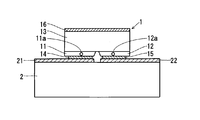
- FIG. 1 is a perspective view of a light emitting device according to an embodiment of the present invention. It is sectional drawing of the light emitting element used as a light source of the light-emitting device by one Embodiment shown in FIG.
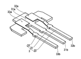
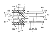
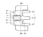
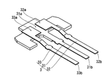
- FIG. 2 is a perspective view of a frame on which a light emitting element of the light emitting device according to the embodiment shown in FIG. 1 is mounted. It is a top view at the time of seeing the light-emitting device by one Embodiment shown in FIG. 1 from the element mounting side (side in which a light emitting element is mounted).
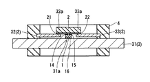
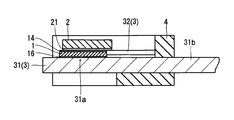
- FIG. 5 is a cross-sectional view taken along line 100-100 in FIG.
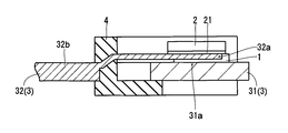
- FIG. 5 is a cross-sectional view taken along line 200-200 in FIG.
- FIG. 5 is a cross-sectional view taken along line 300-300 in FIG.
- FIG. 5 is an enlarged plan view of a part of FIG. 4 (peripheral part of the light emitting element).
- It is a top view at the time of seeing the light-emitting device by one Embodiment shown in FIG. 1 from the back surface side (opposite side to the side in which a light emitting element is mounted).
- It is a perspective view of the flame
- a semiconductor laser element 1 is used as a light emitting element.
- the semiconductor laser element 1 is mounted on the submount 2 and mounted on the frame 3 in that state.
- the semiconductor laser element 1 is an example of the “light emitting element” in the present invention
- the submount 2 is an example of the “base” in the present invention.
- the semiconductor laser element 1 as a light emitting element is a two-wavelength laser element, and includes two semiconductor laser element portions 11 and 12 that generate light of different wavelength bands as shown in FIG.
- each of the semiconductor laser element portions 11 and 12 has an n-type semiconductor layer (such as an n-type cladding layer) and a p-type semiconductor layer (such as a p-type cladding layer and a p-type contact layer).
- the active layer is provided between the p-type semiconductor layer and the p-type semiconductor layer.
- One semiconductor laser element portion 11 is made of, for example, an AlGaInP-based semiconductor and emits a 650 nm band laser beam (an active layer formed between an n-type cladding layer and a p-type cladding layer). (Existing part) 11a.
- the other semiconductor laser element section 12 is made of, for example, an AlGaAs semiconductor and has a light emitting section 12a that emits a laser beam in the 780 nm band.
- These two semiconductor laser element portions 11 and 12 are formed on the main surface (surface facing downward in FIG. 2) of the semiconductor substrate 13 such as an n-type GaAs substrate.
- p-side electrodes 14 and 15 are formed on the surface of the semiconductor laser element portions 11 and 12 opposite to the semiconductor substrate 13 side so as to be separated from each other. Further, an n-side electrode 16 common to the semiconductor laser element portions 11 and 12 is formed on the surface opposite to the main surface of the semiconductor substrate 13. That is, the light emitting portion 11 a of the semiconductor laser element portion 11 is provided between the p-side electrode 14 and the n-side electrode 16, and the light emitting portion 12 a of the semiconductor laser element portion 12 is between the p-side electrode 15 and the n-side electrode 16. Will be provided.
- the p-side electrodes 14 and 15 are examples of the “first electrode” in the present invention, and the n-side electrode 16 is an example of the “second electrode” in the present invention.
- the submount 2 to which the semiconductor laser element 1 is attached is made of ceramics or metal having good thermal conductivity, and has two electrode pads 21 and 22 arranged on the predetermined surface side so as to be insulated from each other. Yes. Of the two electrode pads 21 and 22, the electrode pad 21 is for supplying current to the semiconductor laser element portion 11, and the electrode pad 22 is for supplying current to the semiconductor laser element portion 12.
- the semiconductor laser device 1 is attached to the submount 2 by a junction down method. That is, the p-side electrode 14 of the semiconductor laser element 1 is fixed to the electrode pad 21 of the submount 2 so that the p-side electrode 14 and the electrode pad 21 are electrically connected.
- the electrode 15 is fixed to the electrode pad 22 of the submount 2 so that the p-side electrode 15 and the electrode pad 22 are electrically connected.
- the electrode pads 21 and 22 are an example of the “electrode surface” in the present invention.
- the frame 3 on which the semiconductor laser element 1 is mounted is made of a metal plate (thin plate made of copper, iron, etc.) having excellent thermal conductivity and conductivity. It is obtained by pressing (punching) the plate.
- the frame 3 is a three-terminal frame, and includes a main frame 31 and two sub frames 32 and 33, which are electrically insulated from each other. .
- the main frame 31 is an example of the “first frame” in the present invention
- the sub frames 32 and 33 are examples of the “second frame” in the present invention.
- the main frame 31 is a frame on which the semiconductor laser element 1 is mounted and the n-side electrode 16 (see FIG. 2) of the semiconductor laser element 1 is electrically connected. That is, the main frame 31 has an element mounting portion 31a where the semiconductor laser element 1 is mounted (connected) and a lead portion 31b connected to an external device.
- the sub-frame 32 is a frame to which the p-side electrode 14 (see FIG. 2) of the semiconductor laser element 1 is electrically connected via the electrode pad 21 of the submount 2, and the electrode pad 21 is connected thereto. It has the electrode connection part 32a and the lead part 32b connected to an external apparatus.
- the sub-frame 33 is a frame to which the p-side electrode 15 (see FIG.
- the semiconductor laser element 1 is electrically connected via the electrode pad 22 of the submount 2, and the electrode pad 22 is connected thereto. It has an electrode connection part 33a and a lead part 33b connected to an external device.
- the three lead portions 31b, 32b and 33b of the frame 3 extend toward the side opposite to the light emitting side, and the lead portion 31 of the main frame 31 is provided. They are arranged at a predetermined interval with b as the center.
- the n-side electrode 16 of the semiconductor laser element 1 is directed to the frame 3 side. Then, the n-side electrode 16 of the semiconductor laser element 1 is fixed to the element mounting portion 31a of the main frame 31, so that the n-side electrode 16 of the semiconductor laser element 1 and the element mounting portion 31a of the main frame 31 are electrically connected. It is carried out.
- the p-side electrodes 14 and 15 of the semiconductor laser element 1 are directed to the side opposite to the frame 3 side. For this reason, the electrode pads 21 and 22 of the submount 2 fixed to the p-side electrodes 14 and 15 of the semiconductor laser element 1 face the frame 3 side.
- the electrode pad 21 of the submount 2 is greatly extended toward the light emitting side so that the electrode connection portion 32a of the sub-frame 32 partially overlaps with the plane. That is, when the n-side electrode 16 of the semiconductor laser element 1 is fixed to the element mounting portion 31 a of the main frame 31, a part of the electrode connection portion 32 a of the subframe 32 is covered from the element mounting side by the electrode pad 21 of the submount 2. It will be. Then, in the portion 10 (see FIG.
- the electrode pad 21 of the submount 2 and the electrode connection portion 32a of the subframe 32 overlap in plan view the electrode pad 21 of the submount 2 is connected to the electrode connection portion 32a of the subframe 32.
- the p-side electrode 14 of the semiconductor laser element 1 and the electrode connection portion 32a of the subframe 32 are electrically connected.
- the sub-frame 33 is also processed to have the same shape as the sub-frame 32, and a part of the electrode connection portion 33a overlaps the electrode pad 22 of the sub-mount 2 in a plane. Then, in the portion 10 (see FIG. 8) where the electrode pad 22 of the submount 2 and the electrode connection portion 33a of the subframe 33 overlap in plan view, the electrode pad 22 of the submount 2 is connected to the electrode connection portion 33a of the subframe 33. As a result, the p-side electrode 15 of the semiconductor laser device 1 and the electrode connection portion 33a of the sub-frame 33 are electrically connected.
- the n-side electrode 16 of the semiconductor laser element 1 is electrically connected to the element mounting portion 31a of the main frame 31 without using a bonding wire, and the p-side electrode 14 of the semiconductor laser element 1 is used.
- And 15 are electrically connected to the electrode connecting portions 32a and 33a of the subframes 32 and 33, respectively.
- the electrode connection part 32a of the frame 32 is protruded to the element mounting side from the element mounting part 31a of the main frame 31. Further, by making the thickness of the electrode connection portion 32a of the subframe 32 smaller than the thickness of the lead portion 32b, the thickness of the electrode connection portion 32a of the subframe 32 is made larger than the protruding height of the semiconductor laser element 1 from the submount 2. It is small.
- the processing for the sub frame 32 is also performed for the sub frame 33.
- the electrode connection portion 33a of the subframe 33 protrudes to the element mounting side from the element mounting portion 31a of the main frame 31, and the thickness of the electrode connection portion 33a of the subframe 33 is the submount 2 of the semiconductor laser device 1. It is smaller than the protruding height from.
- the main frame 31 and the sub frames 32 and 33 are fixed to each other by the resin 4.
- the resin 4 When viewed in plan from the element mounting side (see FIG. 4), the resin 4 has a substantially U-shape (a shape surrounding the semiconductor laser element 1 from three directions) in which the light emitting side of the semiconductor laser element 1 is opened. ing.
- the periphery of the region corresponding to the semiconductor laser element 1 is covered with the resin 4, and the region corresponding to the semiconductor laser element 1 is exposed.
- region corresponding to the semiconductor laser element 1 is exposed in the back surface side in order to thermally radiate the heat_generation
- the position of the upper end of the resin 4 is slightly larger than the position of the surface of the submount 2 (the surface opposite to the side on which the semiconductor laser element 1 is attached). It is formed to be higher. In addition, the position of the upper end portion of the resin 4 may be flush with the position of the surface of the submount 2.
- the n-side electrode 16 of the semiconductor laser device 1 and the electrode pads 21 and 22 of the submount 2 are directed to the frame 3 side so that the n-side electrode 16 of the semiconductor laser device 1 is mainly used. It becomes possible to adhere to the element mounting portion 31a of the frame 31, and the n-side electrode 16 of the semiconductor laser element 1 and the element mounting portion 31a of the main frame 31 can be electrically connected without using a bonding wire. .
- the electrode pad 21 of the submount 2 and the electrode connection portion 32a of the subframe 32 are partially overlapped in a plane, so that the electrode pad 21 of the submount 2 is overlapped with the subframe 32 in the plane overlap portion. It can adhere to the electrode connection part 32a.
- the electrical connection between the p-side electrode 14 of the semiconductor laser element 1 (the electrode pad 21 of the submount 2) and the electrode connection portion 32a of the subframe 32 can be performed without using a bonding wire.
- the p-side electrode 15 (electrode pad 22 of the submount 2) of the semiconductor laser element 1 and the subframe 3 The same applies to the electrical connection with the three electrode connection portions 33a, and a bonding wire for electrically connecting them to each other is not necessary. That is, in the present embodiment, it is possible to eliminate the need for a bonding wire in the electrical connection between the semiconductor laser element 1 and the frame 3, and inconveniences caused by using the bonding wire (semiconductor laser caused by disconnection of the bonding wire). It is possible to prevent the occurrence of a connection failure between the element and the frame.
- the light emitting device can be reduced in size (thinned).
- the electrode connection portion 32a of the sub-frame 32 protrudes more toward the device mounting side than the device mounting portion 31a of the main frame 31, so that the p-side of the semiconductor laser device 1 can be easily obtained.
- the electrode 16 can be fixed to the element mounting portion 31 a of the main frame 31, and the electrode pad 21 of the submount 2 can be fixed to the electrode connection portion 32 a of the subframe 32. This effect can also be applied to the other subframe 33.
- the element mounting of the main frame 31 is achieved by making the thickness of the electrode connection portion 32a of the sub-frame 32 smaller than the protruding height of the semiconductor laser element 1 from the submount 2.
- the p-side electrode 16 of the semiconductor laser device 1 is fixed to the element mounting portion 31a of the main frame 31 while suppressing contact (short circuit) between the portion 31a and the electrode connection portion 32a of the subframe 32, and the submount 2
- the electrode pad 21 can be fixed to the electrode connection portion 32 a of the sub frame 32. This effect can also be applied to the other subframe 33.
- the electrode connection portion 32a of the subframe 32 is processed so that the thickness thereof is smaller than the thickness of the lead portion 32b, so that the electrode connection of the subframe 32 is larger than the protruding height of the semiconductor laser element 1 from the submount 2.
- the thickness of the lead portion 32b of the sub-frame 32 can be kept the same as the thickness of the lead portion 31b of the main frame 31.
- the height positions (positions in the thickness direction of the frame 3) of the lead portions 31b and 32b of the main frame 31 and the sub frame 32 can be made uniform. This effect can also be applied to the other subframe 33.
- the entire thickness of the subframe 32 (subframe 33) is made smaller than the protruding height of the semiconductor laser device 1 from the submount 2, and the main frame is adjusted accordingly.
- the thickness of the lead portion 31b of 31 may be made smaller than the thickness of the element mounting portion 31a.
- the present invention is not limited to this, and the semiconductor laser element attached to the light-emitting device is a two-wavelength laser. It does not have to be an element.
Landscapes
- Physics & Mathematics (AREA)
- Condensed Matter Physics & Semiconductors (AREA)
- General Physics & Mathematics (AREA)
- Electromagnetism (AREA)
- Optics & Photonics (AREA)
- Semiconductor Lasers (AREA)
Abstract
【課題】ボンディングワイヤを不要化することが可能な発光装置を提供する。 【解決手段】この発光装置では、半導体レーザ素子1のn側電極16およびサブマウント2の電極パッド21がフレーム3側に向けられているとともに、電極パッド21と副フレーム32の電極接続部32aとが一部で平面的に重畳している。そして、n側電極16が主フレーム31の素子搭載部31aに固着され、電極パッド21が副フレーム32の電極接続部32aに固着されている。
Description
本発明は、発光素子が搭載されるフレームを備えた発光装置に関する。
従来、半導体レーザ素子などの発光素子がフレーム上に搭載された構成の発光装置が知られている(たとえば、特許文献1参照)。以下に、図11を参照して、従来の発光装置の一例について説明する。
従来の発光装置では、図11に示すように、半導体レーザ素子101を発光素子として用いているとともに、その半導体レーザ素子101がジャンクションダウン方式でサブマウント102に取り付けられている。なお、半導体レーザ素子101は2波長レーザ素子であって、p側電極が2つに分離され、n側電極が共通となっている。また、この半導体レーザ素子101のp側電極およびn側電極は、半導体層(発光部)や基板を挟むように形成されている。そして、半導体レーザ素子101のp側電極がサブマウント102に固着され、かつ、電気的に接続されている。
また、サブマウント102に取り付けられた半導体レーザ素子101は、3端子型のフレーム103上に搭載されている。このフレーム103は、互いに電気的に絶縁された1つの主フレーム131と2つの副フレーム132とを含んでおり、それらが樹脂104によって互いに固着された構造となっている。
主フレーム131および副フレーム132のうちの主フレーム131には、サブマウント102が固着されている。そして、ボンディングワイヤ105を介して、半導体レーザ素子101のn側電極と主フレーム131とが電気的に接続されている。また、副フレーム132には、ボンディングワイヤ105を介して、サブマウント102が電気的に接続されている。すなわち、半導体レーザ素子101のp側電極と副フレーム132とが電気的に接続されていることになる。
上記した従来の発光装置では、半導体レーザ素子101とフレーム103との電気的な接続がボンディングワイヤ105を介して行われているが、そのボンディングワイヤ105が外部と接触すると、ボンディングワイヤ105が断線する恐れがある。すなわち、ボンディングワイヤ105を必要とする従来の発光装置では、半導体レーザ素子101とフレーム103との間で接続不良が発生しやすいという不都合がある。
本発明は、上記のような課題を解決するためになされたものであり、ボンディングワイヤを不要化することが可能な発光装置を提供することを目的とする。
上記目的を達成するために、本発明の一の局面による発光装置は、第1電極および第2電極を少なくとも有し、第1電極と第2電極との間に発光部が設けられた発光素子と、発光素子の第1電極が電気的に接続され、かつ、固着される電極面を所定面側に持つ基台と、発光素子が搭載される素子搭載部を有しているとともに、素子搭載部に発光素子の第2電極が電気的に接続される第1フレームと、基台の電極面を介して発光素子の第1電極が電気的に接続される電極接続部を有する第2フレームとを含むフレームとを備えている。そして、発光素子の第2電極および基台の電極面が共にフレーム側に向けられているとともに、基台の電極面と第2フレームの電極接続部とが少なくとも一部で平面的に重畳しており、発光素子の第2電極が第1フレームの素子搭載部に固着され、基台の電極面と第2フレームの電極接続部とが平面的に重畳する部分において基台の電極面が第2フレームの電極接続部に固着されている。
一の局面による発光装置では、上記のように、発光素子の第2電極および基台の電極面を共にフレーム側に向け、発光素子の第2電極を第1フレームの素子搭載部に固着することによって、ボンディングワイヤを用いることなく、発光素子の第2電極と第1フレームの素子搭載部とを電気的に接続することができる。また、基台の電極面と第2フレームの電極接続部とを少なくとも一部で平面的に重畳させ、基台の電極面と第2フレームの電極接続部とが平面的に重畳する部分において基台の電極面を第2フレームの電極接続部に固着することによって、発光素子の第1電極(基台の電極面)と第2フレームの電極接続部との電気的な接続についても、ボンディングワイヤを用いずに行うことができる。すなわち、一の局面による発光装置では、発光素子とフレームとの電気的な接続においてボンディングワイヤの不要化を図ることができ、ボンディングワイヤを用いることで起こる不都合(ボンディングワイヤの断線に起因する発光素子とフレームとの間の接続不良)の発生
を防止することが可能となる。また、一の局面による発光装置では、ボンディングワイヤが不要となるので、ボンディングワイヤのためのスペースを省略することができる。このため、発光装置の小型化(薄型化)を図ることも可能となる。
上記一の局面による発光装置において、第2フレームの電極接続部が第1フレームの素子搭載部よりも素子搭載側に突出していることが好ましい。このように構成すれば、容易に、発光素子の第2電極(基台の電極面から突出した部分)を第1フレームの素子搭載部に固着し、基台の電極面を第2フレームの電極接続部に固着することができる。
を防止することが可能となる。また、一の局面による発光装置では、ボンディングワイヤが不要となるので、ボンディングワイヤのためのスペースを省略することができる。このため、発光装置の小型化(薄型化)を図ることも可能となる。
上記一の局面による発光装置において、第2フレームの電極接続部が第1フレームの素子搭載部よりも素子搭載側に突出していることが好ましい。このように構成すれば、容易に、発光素子の第2電極(基台の電極面から突出した部分)を第1フレームの素子搭載部に固着し、基台の電極面を第2フレームの電極接続部に固着することができる。
この場合、第2フレームの一部が曲げられることにより、第2フレームの電極接続部が第1フレームの素子搭載部よりも素子搭載側に突出されていることが好ましい。このように構成すれば、容易に、第2フレームの電極接続部が第1フレームの素子搭載部よりも素子搭載側に突出された状態にすることができる。
上記一の局面による発光装置において、基台の電極面からの発光素子の突出高さよりも第2フレームの電極接続部の厚みの方が小さいことが好ましい。このように構成すれば、第1フレームの素子搭載部と第2フレームの電極接続部とが接触(短絡)するのを抑制しながら、発光素子の第2電極(基台の電極面から突出した部分)を第1フレームの素子搭載部に固着し、基台の電極面を第2フレームの電極接続部に固着することができる。
上記一の局面による発光装置において、第1フレームおよび第2フレームが樹脂を介して互いに固着されていることが好ましい。
上記一の局面による発光装置において、好ましくは、発光素子が半導体レーザ素子である。
以上のように、本発明によれば、ボンディングワイヤを不要化することが可能な発光装置を容易に得ることができる。
以下に、図1~図9を参照して、本実施形態による発光装置の構成について説明する。
本実施形態の発光装置では、図1に示すように、半導体レーザ素子1を発光素子として用いている。そして、その半導体レーザ素子1は、サブマウント2に取り付けられているとともに、その状態でフレーム3上に搭載されている。なお、半導体レーザ素子1は、本発明の「発光素子」の一例であり、サブマウント2は、本発明の「基台」の一例である。
発光素子としての半導体レーザ素子1は2波長レーザ素子であり、図2に示すように、互いに異なる波長帯の光を生成する2つの半導体レーザ素子部11および12を含んでいる。半導体レーザ素子部11および12は、図示しないが、n型半導体層(n型クラッド層など)やp型半導体層(p型クラッド層やp型コンタクト層など)をそれぞれ有しており、そのn型半導体層とp型半導体層との間に活性層が設けられた構造となっている。一方の半導体レーザ素子部11は、たとえば、AlGaInP系半導体からなっており、650nm帯のレーザ光を発光する発光部(n型クラッド層とp型クラッド層との間に形成されている活性層が存在する部分)11aを持っている。他方の半導体レーザ素子部12は、たとえば、AlGaAs系半導体からなっており、780nm帯のレーザ光を発光する発光部12aを持っている。そして、これら2つの半導体レーザ素子部11および12は、n型GaAs基板などの半導体基板13の主面(図2において下方に向いている面)上に形成されている。
また、半導体レーザ素子部11および12の半導体基板13側とは反対側の面上には、それぞれ、p側電極14および15が互いに分離するように形成されている。さらに、半導体基板13の主面とは反対側の面上には、半導体レーザ素子部11および12で共通のn側電極16が形成されている。すなわち、半導体レーザ素子部11の発光部11aがp側電極14とn側電極16との間に設けられ、半導体レーザ素子部12の発光部12aがp側電極15とn側電極16との間に設けられていることになる。なお、p側電極14および15は、本発明の「第1電極」の一例であり、n側電極16は、本発明の「第2電極」の一例である。
半導体レーザ素子1が取り付けられるサブマウント2は、熱伝導性が良好なセラミックスや金属などからなっているとともに、互いに絶縁分離して配置された2つの電極パッド21および22を所定面側に持っている。2つの電極パッド21および22のうちの電極パッド21は半導体レーザ素子部11に電流を供給するためのものであり、電極パッド22は半導体レーザ素子部12に電流を供給するためのものである。そして、このサブマウント2に対する半導体レーザ素子1の取り付けは、ジャンクションダウン方式によってなされている。すなわち、半導体レーザ素子1のp側電極14がサブマウント2の電極パッド21に固着されることでp側電極14と電極パッド21とが電気的に接続されており、半導体レーザ素子1のp側電極15がサブマウント2の電極パッド22に固着されることでp側電極15と電極パッド22とが電気的に接続されている。なお、電極パッド21および22は、本発明の「電極面」の一例である。
また、図1および図3に示すように、半導体レーザ素子1が搭載されるフレーム3は、熱伝導性および導電性に優れた金属板(銅や鉄などからなる薄板)からなっており、金属板をプレス加工(打ち抜き加工)することで得ている。また、このフレーム3は、3端子型のフレームであって、1つの主フレーム31と2つの副フレーム32および33とを含んでいるとともに、それらが互いに電気的に絶縁された構造となっている。なお、主フレーム31は、本発明の「第1フレーム」の一例であり、副フレーム32および33は、本発明の「第2フレーム」の一例である。
主フレーム31は、半導体レーザ素子1が搭載され、かつ、半導体レーザ素子1のn側電極16(図2参照)が電気的に接続されるフレームである。すなわち、主フレーム31は、半導体レーザ素子1が搭載(接続)される素子搭載部31aと、外部機器に接続されるリード部31bとを有している。また、副フレーム32は、半導体レーザ素子1のp側電極14(図2参照)がサブマウント2の電極パッド21を介して電気的に接続されるフレームであって、電極パッド21が接続される電極接続部32aと、外部機器に接続されるリード部32bとを有している。また、副フレーム33は、半導体レーザ素子1のp側電極15(図2参照)がサブマウント2の電極パッド22を介して電気的に接続されるフレームであって、電極パッド22が接続される電極接続部33aと、外部機器に接続されるリード部33bとを有している。このフレーム3の3本のリード部31b、32bおよび33bは、光出射側とは反対側に向かって延びており、主フレーム31のリード部31
bを中心として互いに所定の間隔を隔てて配置されている。
bを中心として互いに所定の間隔を隔てて配置されている。
ここで、本実施形態では、図4~図6に示すように、半導体レーザ素子1のn側電極16がフレーム3側に向けられている。そして、半導体レーザ素子1のn側電極16を主フレーム31の素子搭載部31aに固着することにより、半導体レーザ素子1のn側電極16と主フレーム31の素子搭載部31aとの電気的な接続を行っている。ところで、半導体レーザ素子1のn側電極16をフレーム3側に向けた場合には、半導体レーザ素子1のp側電極14および15がフレーム3側とは反対側に向く。このため、その半導体レーザ素子1のp側電極14および15のそれぞれと固着しているサブマウント2の電極パッド21および22がフレーム3側に向くことになる。
さらに、本実施形態では、図3~図8に示すように、半導体レーザ素子1のn側電極16が主フレーム31の素子搭載部31aに固着された状態において、サブマウント2の電極パッド21と副フレーム32の電極接続部32aとが一部で平面的に重畳するように、副フレーム32が光出射側に向かって大きく延ばされている。すなわち、半導体レーザ素子1のn側電極16を主フレーム31の素子搭載部31aに固着すると、副フレーム32の電極接続部32aの一部がサブマウント2の電極パッド21によって素子搭載側から覆われることになる。そして、サブマウント2の電極パッド21と副フレーム32の電極接続部32aとが平面的に重畳する部分10(図8参照)において、サブマウント2の電極パッド21を副フレーム32の電極接続部32aに固着することによって、半導体レーザ素子1のp側電極14と副フレーム32の電極接続部32aとの電気的な接続を行っている。
なお、副フレーム33についても、副フレーム32と同様な形状となるように加工されており、その電極接続部33aの一部がサブマウント2の電極パッド22と平面的に重畳している。そして、サブマウント2の電極パッド22と副フレーム33の電極接続部33aとが平面的に重畳する部分10(図8参照)において、サブマウント2の電極パッド22を副フレーム33の電極接続部33aに固着することによって、半導体レーザ素子1のp側電極15と副フレーム33の電極接続部33aとの電気的な接続を行っている。
このように、本実施形態では、ボンディングワイヤを用いずに、半導体レーザ素子1のn側電極16が主フレーム31の素子搭載部31aに電気的に接続され、半導体レーザ素子1のp側電極14および15(サブマウント2の電極パッド21および22)のそれぞれが副フレーム32および33の電極接続部32aおよび33aに電気的に接続された構成となっている。
また、本実施形態では、図3および図7に示すように、副フレーム32の電極接続部32aとリード部32bとの間の部分(後述する樹脂4で覆われる部分)を曲げることによって、副フレーム32の電極接続部32aを主フレーム31の素子搭載部31aよりも素子搭載側に突出させている。また、副フレーム32の電極接続部32aの厚みをリード部32bの厚みよりも小さくすることによって、副フレーム32の電極接続部32aの厚みを半導体レーザ素子1のサブマウント2からの突出高さよりも小さくしている。なお、この副フレーム32に対する加工は、副フレーム33に対しても施されている。すなわち、副フレーム33の電極接続部33aが主フレーム31の素子搭載部31aよりも素子搭載側に突出しているとともに、その副フレーム33の電極接続部33aの厚みが半導体レーザ素子1のサブマウント2からの突出高さよりも小さくなっている。
また、図4および図9に示すように、主フレーム31、副フレーム32および33は、樹脂4によって互いに固着されている。この樹脂4は、素子搭載側から平面視(図4参照)すると、半導体レーザ素子1の光出射側が開放された略コの字状(半導体レーザ素子1を3方向から囲むような形状)になっている。
また、裏面側から平面視(図9参照)した場合には、半導体レーザ素子1に対応する領域の周辺が樹脂4によって覆われており、半導体レーザ素子1に対応する領域は露出されている。このように、裏面側において半導体レーザ素子1に対応する領域を露出させているのは、半導体レーザ素子1の発熱を効率良く放熱するためである。
また、樹脂4は、図5~図7に示すように、その上端部の位置がサブマウント2の表面(半導体レーザ素子1が取り付けられている側とは反対側の面)の位置よりも若干高くなるように形成されている。なお、樹脂4の上端部の位置としては、サブマウント2の表面の位置に対して面一となっていてもよい。
本実施形態では、上記のように、半導体レーザ素子1のn側電極16とサブマウント2の電極パッド21および22とをフレーム3側に向けることによって、半導体レーザ素子1のn側電極16を主フレーム31の素子搭載部31aに固着することが可能となり、ボンディングワイヤを用いることなく、半導体レーザ素子1のn側電極16と主フレーム31の素子搭載部31aとを電気的に接続することができる。また、サブマウント2の電極パッド21と副フレーム32の電極接続部32aとを一部で平面的に重畳させることによって、その平面的に重畳する部分においてサブマウント2の電極パッド21を副フレーム32の電極接続部32aに固着することができる。これにより、半導体レーザ素子1のp側電極14(サブマウント2の電極パッド21)と副フレーム32の電極接続部32aとの電気的な接続についても、ボンディングワイヤを用いずに行うことができる。さらに、半導体レーザ素子1のp側電極15(サブマウント2の電極パッド22)と副フレーム3
3の電極接続部33aとの電気的な接続についても同様であって、それらを互いに電気的に接続するためのボンディングワイヤが必要なくなる。すなわち、本実施形態では、半導体レーザ素子1とフレーム3との電気的な接続においてボンディングワイヤの不要化を図ることができ、ボンディングワイヤを用いることで起こる不都合(ボンディングワイヤの断線に起因する半導体レーザ素子とフレームとの間の接続不良)の発生を防止することが可能となる。
3の電極接続部33aとの電気的な接続についても同様であって、それらを互いに電気的に接続するためのボンディングワイヤが必要なくなる。すなわち、本実施形態では、半導体レーザ素子1とフレーム3との電気的な接続においてボンディングワイヤの不要化を図ることができ、ボンディングワイヤを用いることで起こる不都合(ボンディングワイヤの断線に起因する半導体レーザ素子とフレームとの間の接続不良)の発生を防止することが可能となる。
なお、本実施形態では、ボンディングワイヤが不要となるので、ボンディングワイヤのためのスペースを省略することができる。すなわち、樹脂4の上端部の位置を従来よりも低くすることができる。したがって、本実施形態では、発光装置の小型化(薄型化)を図ることも可能となる。
また、本実施形態では、上記のように、副フレーム32の電極接続部32aを主フレーム31の素子搭載部31aよりも素子搭載側に突出させることによって、容易に、半導体レーザ素子1のp側電極16を主フレーム31の素子搭載部31aに固着し、サブマウント2の電極パッド21を副フレーム32の電極接続部32aに固着することができる。なお、この効果は、もう1つの副フレーム33についても言える。
また、本実施形態では、上記のように、半導体レーザ素子1のサブマウント2からの突出高さよりも副フレーム32の電極接続部32aの厚みの方を小さくすることによって、主フレーム31の素子搭載部31aと副フレーム32の電極接続部32aとが接触(短絡)するのを抑制しながら、半導体レーザ素子1のp側電極16を主フレーム31の素子搭載部31aに固着し、サブマウント2の電極パッド21を副フレーム32の電極接続部32aに固着することができる。なお、この効果は、もう1つの副フレーム33についても言える。
この場合、副フレーム32の電極接続部32aの厚みがリード部32bの厚みよりも小さくなるように加工することで、半導体レーザ素子1のサブマウント2からの突出高さよりも副フレーム32の電極接続部32aの厚みの方を小さくすることによって、副フレーム32のリード部32bの厚みについては主フレーム31のリード部31bの厚みと同じままにしておくことができる。このため、主フレーム31および副フレーム32のそれぞれのリード部31bおよび32bの高さ位置(フレーム3の厚み方向の位置)を揃えることができる。なお、この効果は、もう1つの副フレーム33についても言える。
なお、上記した構成において、図10に示すように、副フレーム32(副フレーム33)の全体の厚みを半導体レーザ素子1のサブマウント2からの突出高さよりも小さくし、それに合わせて、主フレーム31のリード部31bの厚みを素子搭載部31aの厚みよりも小さくするようにしてもよい。
今回開示された実施形態は、すべての点で例示であって制限的なものではないと考えられるべきである。本発明の範囲は、上記した実施形態の説明ではなく特許請求の範囲によって示され、さらに、特許請求の範囲と均等の意味および範囲内でのすべての変更が含まれる。
たとえば、上記実施形態では、2波長レーザ素子が装着された発光装置に本発明を適用する例について説明したが、本発明はこれに限らず、発光装置に装着される半導体レーザ素子が2波長レーザ素子でなくてもよい。
1 半導体レーザ素子(発光素子)
2 サブマウント(基台)
3 フレーム
4 樹脂
11a、12a 発光部
14、15 p側電極(第1電極)
16 n側電極(第2電極)
21、22 電極パッド(電極面)
31 主フレーム(第1フレーム)
31a 素子搭載部
32、33 副フレーム(第2フレーム)
32a、33a 電極接続部
2 サブマウント(基台)
3 フレーム
4 樹脂
11a、12a 発光部
14、15 p側電極(第1電極)
16 n側電極(第2電極)
21、22 電極パッド(電極面)
31 主フレーム(第1フレーム)
31a 素子搭載部
32、33 副フレーム(第2フレーム)
32a、33a 電極接続部
Claims (6)
- 第1電極および第2電極を少なくとも有し、前記第1電極と前記第2電極との間に発光部が設けられた発光素子と、
前記発光素子の第1電極が電気的に接続され、かつ、固着される電極面を所定面側に持つ基台と、
前記発光素子が搭載される素子搭載部を有しているとともに、前記素子搭載部に前記発光素子の第2電極が電気的に接続される第1フレームと、前記基台の電極面を介して前記発光素子の第1電極が電気的に接続される電極接続部を有する第2フレームとを含むフレームとを備え、
前記発光素子の第2電極および前記基台の電極面が共に前記フレーム側に向けられているとともに、前記基台の電極面と前記第2フレームの電極接続部とが少なくとも一部で平面的に重畳しており、
前記発光素子の第2電極が前記第1フレームの素子搭載部に固着され、前記基台の電極面と前記第2フレームの電極接続部とが平面的に重畳する部分において前記基台の電極面が前記第2フレームの電極接続部に固着されていることを特徴とする発光装置。 - 前記第2フレームの電極接続部が前記第1フレームの素子搭載部よりも素子搭載側に突出していることを特徴とする請求項1に記載の発光装置。
- 前記第2フレームの一部が曲げられることにより、前記第2フレームの電極接続部が前記第1フレームの素子搭載部よりも素子搭載側に突出されていることを特徴とする請求項2に記載の発光装置。
- 前記基台の電極面からの前記発光素子の突出高さよりも前記第2フレームの電極接続部の厚みの方が小さいことを特徴とする請求項1~3のいずれかに記載の発光装置。
- 前記第1フレームおよび前記第2フレームが樹脂を介して互いに固着されていることを特徴とする請求項1~4のいずれかに記載の発光装置。
- 前記発光素子が半導体レーザ素子であることを特徴とする請求項1~5のいずれかに記載の発光装置。
Applications Claiming Priority (2)
| Application Number | Priority Date | Filing Date | Title |
|---|---|---|---|
| JP2009-005445 | 2009-01-14 | ||
| JP2009005445 | 2009-01-14 |
Publications (1)
| Publication Number | Publication Date |
|---|---|
| WO2010082401A1 true WO2010082401A1 (ja) | 2010-07-22 |
Family
ID=42339660
Family Applications (1)
| Application Number | Title | Priority Date | Filing Date |
|---|---|---|---|
| PCT/JP2009/070014 Ceased WO2010082401A1 (ja) | 2009-01-14 | 2009-11-27 | 発光装置 |
Country Status (1)
| Country | Link |
|---|---|
| WO (1) | WO2010082401A1 (ja) |
Cited By (1)
| Publication number | Priority date | Publication date | Assignee | Title |
|---|---|---|---|---|
| CN106898944A (zh) * | 2017-03-01 | 2017-06-27 | 苏州达沃特光电科技有限公司 | 一种高效散热的单芯半导体激光器封装结构及方法 |
Citations (3)
| Publication number | Priority date | Publication date | Assignee | Title |
|---|---|---|---|---|
| JPS62204365U (ja) * | 1986-06-18 | 1987-12-26 | ||
| JP2001036180A (ja) * | 1999-07-23 | 2001-02-09 | Sharp Corp | 半導体レーザ装置およびその製造方法 |
| JP2008021754A (ja) * | 2006-07-12 | 2008-01-31 | Sanyo Electric Co Ltd | フレームパッケージ型半導体レーザ装置 |
-
2009
- 2009-11-27 WO PCT/JP2009/070014 patent/WO2010082401A1/ja not_active Ceased
Patent Citations (3)
| Publication number | Priority date | Publication date | Assignee | Title |
|---|---|---|---|---|
| JPS62204365U (ja) * | 1986-06-18 | 1987-12-26 | ||
| JP2001036180A (ja) * | 1999-07-23 | 2001-02-09 | Sharp Corp | 半導体レーザ装置およびその製造方法 |
| JP2008021754A (ja) * | 2006-07-12 | 2008-01-31 | Sanyo Electric Co Ltd | フレームパッケージ型半導体レーザ装置 |
Cited By (1)
| Publication number | Priority date | Publication date | Assignee | Title |
|---|---|---|---|---|
| CN106898944A (zh) * | 2017-03-01 | 2017-06-27 | 苏州达沃特光电科技有限公司 | 一种高效散热的单芯半导体激光器封装结构及方法 |
Similar Documents
| Publication | Publication Date | Title |
|---|---|---|
| JP4160597B2 (ja) | 半導体発光素子及びその製造方法 | |
| JP5535750B2 (ja) | 発光素子モジュール | |
| JP2007027716A (ja) | レーザダイオード素子のためのパッケージ、レーザダイオード素子ならびにレーザダイオード素子を製作する方法 | |
| TWI492355B (zh) | 半導體封裝 | |
| US9780523B2 (en) | Semiconductor laser device | |
| CN103227410B (zh) | 半导体激光装置 | |
| WO2017072849A1 (ja) | レーザ光源モジュール | |
| JP2015135911A (ja) | 半導体光素子及び光モジュール | |
| TWI517509B (zh) | Multi - beam semiconductor laser device | |
| JP2010192672A (ja) | 面発光レーザ | |
| JP2004055744A (ja) | 半導体レーザ装置 | |
| JP2011077338A (ja) | 発光装置およびその製造方法 | |
| US11588296B2 (en) | Package, light-emitting device, and laser device | |
| JP2019062033A (ja) | 半導体レーザ装置 | |
| JP2010010345A (ja) | 半導体パッケージおよび半導体発光装置 | |
| JP2022078403A (ja) | 半導体レーザ装置および半導体レーザ装置の製造方法 | |
| JP2009199977A (ja) | 照明装置 | |
| US7873086B2 (en) | Semiconductor device | |
| TW202146954A (zh) | 光電混載基板及光電複合傳送模組 | |
| JP2007027375A (ja) | レーザモジュール | |
| JP2010073774A (ja) | 半導体レーザ装置 | |
| KR101327243B1 (ko) | 바형태의 레이저 다이오드 어레이를 개별 구동하기 위한 p형 서브마운트 및 이를 포함하는 반도체 패키지 | |
| JP2011222626A (ja) | 半導体発光装置および発光素子パッケージ | |
| JP4238864B2 (ja) | 半導体装置および半導体装置の製造方法 | |
| JP2021028919A (ja) | 半導体レーザ装置 |
Legal Events
| Date | Code | Title | Description |
|---|---|---|---|
| 121 | Ep: the epo has been informed by wipo that ep was designated in this application |
Ref document number: 09838367 Country of ref document: EP Kind code of ref document: A1 |
|
| NENP | Non-entry into the national phase |
Ref country code: DE |
|
| 122 | Ep: pct application non-entry in european phase |
Ref document number: 09838367 Country of ref document: EP Kind code of ref document: A1 |
|
| NENP | Non-entry into the national phase |
Ref country code: JP |