WO2010073497A1 - 半導体装置 - Google Patents
半導体装置 Download PDFInfo
- Publication number
- WO2010073497A1 WO2010073497A1 PCT/JP2009/006548 JP2009006548W WO2010073497A1 WO 2010073497 A1 WO2010073497 A1 WO 2010073497A1 JP 2009006548 W JP2009006548 W JP 2009006548W WO 2010073497 A1 WO2010073497 A1 WO 2010073497A1
- Authority
- WO
- WIPO (PCT)
- Prior art keywords
- lead
- island
- resin package
- semiconductor device
- aforementioned
- Prior art date
- Legal status (The legal status is an assumption and is not a legal conclusion. Google has not performed a legal analysis and makes no representation as to the accuracy of the status listed.)
- Ceased
Links
Images




Classifications
-
- H—ELECTRICITY
- H10—SEMICONDUCTOR DEVICES; ELECTRIC SOLID-STATE DEVICES NOT OTHERWISE PROVIDED FOR
- H10W—GENERIC PACKAGES, INTERCONNECTIONS, CONNECTORS OR OTHER CONSTRUCTIONAL DETAILS OF DEVICES COVERED BY CLASS H10
- H10W70/00—Package substrates; Interposers; Redistribution layers [RDL]
- H10W70/40—Leadframes
- H10W70/421—Shapes or dispositions
- H10W70/424—Cross-sectional shapes
-
- H—ELECTRICITY
- H10—SEMICONDUCTOR DEVICES; ELECTRIC SOLID-STATE DEVICES NOT OTHERWISE PROVIDED FOR
- H10W—GENERIC PACKAGES, INTERCONNECTIONS, CONNECTORS OR OTHER CONSTRUCTIONAL DETAILS OF DEVICES COVERED BY CLASS H10
- H10W70/00—Package substrates; Interposers; Redistribution layers [RDL]
- H10W70/40—Leadframes
- H10W70/411—Chip-supporting parts, e.g. die pads
-
- H—ELECTRICITY
- H10—SEMICONDUCTOR DEVICES; ELECTRIC SOLID-STATE DEVICES NOT OTHERWISE PROVIDED FOR
- H10W—GENERIC PACKAGES, INTERCONNECTIONS, CONNECTORS OR OTHER CONSTRUCTIONAL DETAILS OF DEVICES COVERED BY CLASS H10
- H10W70/00—Package substrates; Interposers; Redistribution layers [RDL]
- H10W70/40—Leadframes
- H10W70/421—Shapes or dispositions
-
- H—ELECTRICITY
- H10—SEMICONDUCTOR DEVICES; ELECTRIC SOLID-STATE DEVICES NOT OTHERWISE PROVIDED FOR
- H10W—GENERIC PACKAGES, INTERCONNECTIONS, CONNECTORS OR OTHER CONSTRUCTIONAL DETAILS OF DEVICES COVERED BY CLASS H10
- H10W70/00—Package substrates; Interposers; Redistribution layers [RDL]
- H10W70/40—Leadframes
- H10W70/464—Additional interconnections in combination with leadframes
- H10W70/465—Bumps or wires
-
- H—ELECTRICITY
- H10—SEMICONDUCTOR DEVICES; ELECTRIC SOLID-STATE DEVICES NOT OTHERWISE PROVIDED FOR
- H10W—GENERIC PACKAGES, INTERCONNECTIONS, CONNECTORS OR OTHER CONSTRUCTIONAL DETAILS OF DEVICES COVERED BY CLASS H10
- H10W72/00—Interconnections or connectors in packages
-
- H—ELECTRICITY
- H10—SEMICONDUCTOR DEVICES; ELECTRIC SOLID-STATE DEVICES NOT OTHERWISE PROVIDED FOR
- H10W—GENERIC PACKAGES, INTERCONNECTIONS, CONNECTORS OR OTHER CONSTRUCTIONAL DETAILS OF DEVICES COVERED BY CLASS H10
- H10W72/00—Interconnections or connectors in packages
- H10W72/50—Bond wires
-
- H—ELECTRICITY
- H10—SEMICONDUCTOR DEVICES; ELECTRIC SOLID-STATE DEVICES NOT OTHERWISE PROVIDED FOR
- H10W—GENERIC PACKAGES, INTERCONNECTIONS, CONNECTORS OR OTHER CONSTRUCTIONAL DETAILS OF DEVICES COVERED BY CLASS H10
- H10W74/00—Encapsulations, e.g. protective coatings
- H10W74/10—Encapsulations, e.g. protective coatings characterised by their shape or disposition
- H10W74/111—Encapsulations, e.g. protective coatings characterised by their shape or disposition the semiconductor body being completely enclosed
-
- H—ELECTRICITY
- H10—SEMICONDUCTOR DEVICES; ELECTRIC SOLID-STATE DEVICES NOT OTHERWISE PROVIDED FOR
- H10W—GENERIC PACKAGES, INTERCONNECTIONS, CONNECTORS OR OTHER CONSTRUCTIONAL DETAILS OF DEVICES COVERED BY CLASS H10
- H10W74/00—Encapsulations, e.g. protective coatings
- H10W74/10—Encapsulations, e.g. protective coatings characterised by their shape or disposition
- H10W74/111—Encapsulations, e.g. protective coatings characterised by their shape or disposition the semiconductor body being completely enclosed
- H10W74/129—Encapsulations, e.g. protective coatings characterised by their shape or disposition the semiconductor body being completely enclosed forming a chip-scale package [CSP]
-
- H—ELECTRICITY
- H10—SEMICONDUCTOR DEVICES; ELECTRIC SOLID-STATE DEVICES NOT OTHERWISE PROVIDED FOR
- H10W—GENERIC PACKAGES, INTERCONNECTIONS, CONNECTORS OR OTHER CONSTRUCTIONAL DETAILS OF DEVICES COVERED BY CLASS H10
- H10W74/00—Encapsulations, e.g. protective coatings
- H10W74/40—Encapsulations, e.g. protective coatings characterised by their materials
- H10W74/47—Encapsulations, e.g. protective coatings characterised by their materials comprising organic materials, e.g. plastics or resins
-
- H—ELECTRICITY
- H10—SEMICONDUCTOR DEVICES; ELECTRIC SOLID-STATE DEVICES NOT OTHERWISE PROVIDED FOR
- H10W—GENERIC PACKAGES, INTERCONNECTIONS, CONNECTORS OR OTHER CONSTRUCTIONAL DETAILS OF DEVICES COVERED BY CLASS H10
- H10W72/00—Interconnections or connectors in packages
- H10W72/50—Bond wires
- H10W72/541—Dispositions of bond wires
- H10W72/5445—Dispositions of bond wires being orthogonal to a side surface of the chip, e.g. parallel arrangements
-
- H—ELECTRICITY
- H10—SEMICONDUCTOR DEVICES; ELECTRIC SOLID-STATE DEVICES NOT OTHERWISE PROVIDED FOR
- H10W—GENERIC PACKAGES, INTERCONNECTIONS, CONNECTORS OR OTHER CONSTRUCTIONAL DETAILS OF DEVICES COVERED BY CLASS H10
- H10W72/00—Interconnections or connectors in packages
- H10W72/851—Dispositions of multiple connectors or interconnections
- H10W72/874—On different surfaces
- H10W72/884—Die-attach connectors and bond wires
-
- H—ELECTRICITY
- H10—SEMICONDUCTOR DEVICES; ELECTRIC SOLID-STATE DEVICES NOT OTHERWISE PROVIDED FOR
- H10W—GENERIC PACKAGES, INTERCONNECTIONS, CONNECTORS OR OTHER CONSTRUCTIONAL DETAILS OF DEVICES COVERED BY CLASS H10
- H10W72/00—Interconnections or connectors in packages
- H10W72/90—Bond pads, in general
- H10W72/951—Materials of bond pads
-
- H—ELECTRICITY
- H10—SEMICONDUCTOR DEVICES; ELECTRIC SOLID-STATE DEVICES NOT OTHERWISE PROVIDED FOR
- H10W—GENERIC PACKAGES, INTERCONNECTIONS, CONNECTORS OR OTHER CONSTRUCTIONAL DETAILS OF DEVICES COVERED BY CLASS H10
- H10W74/00—Encapsulations, e.g. protective coatings
-
- H—ELECTRICITY
- H10—SEMICONDUCTOR DEVICES; ELECTRIC SOLID-STATE DEVICES NOT OTHERWISE PROVIDED FOR
- H10W—GENERIC PACKAGES, INTERCONNECTIONS, CONNECTORS OR OTHER CONSTRUCTIONAL DETAILS OF DEVICES COVERED BY CLASS H10
- H10W76/00—Containers; Fillings or auxiliary members therefor; Seals
- H10W76/10—Containers or parts thereof
- H10W76/12—Containers or parts thereof characterised by their shape
-
- H—ELECTRICITY
- H10—SEMICONDUCTOR DEVICES; ELECTRIC SOLID-STATE DEVICES NOT OTHERWISE PROVIDED FOR
- H10W—GENERIC PACKAGES, INTERCONNECTIONS, CONNECTORS OR OTHER CONSTRUCTIONAL DETAILS OF DEVICES COVERED BY CLASS H10
- H10W90/00—Package configurations
- H10W90/701—Package configurations characterised by the relative positions of pads or connectors relative to package parts
- H10W90/731—Package configurations characterised by the relative positions of pads or connectors relative to package parts of die-attach connectors
- H10W90/736—Package configurations characterised by the relative positions of pads or connectors relative to package parts of die-attach connectors between a chip and a stacked lead frame, conducting package substrate or heat sink
-
- H—ELECTRICITY
- H10—SEMICONDUCTOR DEVICES; ELECTRIC SOLID-STATE DEVICES NOT OTHERWISE PROVIDED FOR
- H10W—GENERIC PACKAGES, INTERCONNECTIONS, CONNECTORS OR OTHER CONSTRUCTIONAL DETAILS OF DEVICES COVERED BY CLASS H10
- H10W90/00—Package configurations
- H10W90/701—Package configurations characterised by the relative positions of pads or connectors relative to package parts
- H10W90/751—Package configurations characterised by the relative positions of pads or connectors relative to package parts of bond wires
- H10W90/755—Package configurations characterised by the relative positions of pads or connectors relative to package parts of bond wires between a chip and a laterally-adjacent insulating package substrate, interpose or RDL
-
- H—ELECTRICITY
- H10—SEMICONDUCTOR DEVICES; ELECTRIC SOLID-STATE DEVICES NOT OTHERWISE PROVIDED FOR
- H10W—GENERIC PACKAGES, INTERCONNECTIONS, CONNECTORS OR OTHER CONSTRUCTIONAL DETAILS OF DEVICES COVERED BY CLASS H10
- H10W90/00—Package configurations
- H10W90/701—Package configurations characterised by the relative positions of pads or connectors relative to package parts
- H10W90/751—Package configurations characterised by the relative positions of pads or connectors relative to package parts of bond wires
- H10W90/756—Package configurations characterised by the relative positions of pads or connectors relative to package parts of bond wires between a chip and a stacked lead frame, conducting package substrate or heat sink
Definitions
- the present invention relates to a surface-mount type semiconductor device.
- a semiconductor device employing a non-lead package has a structure in which a semiconductor chip is sealed with a resin package together with a lead frame.
- the lead frame is formed by punching a thin metal plate, and includes an island and a plurality of leads arranged around the island.
- the semiconductor chip is die-bonded to the upper surface of the island, and is electrically connected to each lead by a bonding wire laid between the surface and the upper surface of each lead.
- the island and the lower surface of each lead are exposed on the back surface of the resin package.
- an object of the present invention is to provide a surface-mount type semiconductor device capable of improving the bonding strength between a lead and a resin package.
- a semiconductor device includes a semiconductor chip, an island to which the semiconductor chip is bonded to an upper surface, leads arranged around the island, a surface of the semiconductor chip, and the leads. And a resin package that collectively seals the semiconductor chip, the island, the lead, and the bonding wire, and the lower surface of the island and the lower surface of the lead are It is exposed on the back surface of the resin package, and the lead is formed with a recess that is recessed from the lower surface side and is opened on the side surface.
- the semiconductor device In this semiconductor device, the islands to which the semiconductor chip is bonded (die bonding) and the lower surfaces of the leads electrically connected to the semiconductor chip by bonding wires are exposed on the back surface of the resin package that collectively seals them. ing. Therefore, the semiconductor device can be surface-mounted on a wiring board.
- the lead is formed with a recess that is recessed from the lower surface side and is open on the side surface. When the resin package material enters the recess, part of the peripheral edge of the lead is sandwiched between the upper and lower sides of the resin package. Thereby, the joint strength between the lead and the resin package can be improved. As a result, it is possible to prevent the lead from dropping from the resin package.
- the concave portion has an arcuate portion in a bottom view.
- the concave portion has an arcuate portion in a bottom view.
- the concave portion is opened on a side surface facing the island in the lead.
- the resin package material can surely enter the concave portion, so that the bonding strength between the lead and the resin package can be reliably improved.
- the island may have a quadrangular shape when viewed from the bottom, and the leads may be disposed in portions facing the four sides of the island when viewed from the bottom, and may have a shape having sides parallel to the facing sides. Good.
- the recess is opened on the side surface having the side facing each side of the island in each lead. Thereby, since the material of the resin package can surely enter the concave portion of each lead, the bonding strength between each lead and the resin package can be reliably improved.
- the area of the concave portion in a bottom view is 1/2 or less of the total area of the lower surface of the lead.
- the lead has a side surface exposed at the side surface of the resin package, and a concave groove recessed from the lower surface side of the lead is formed in a portion along the exposed side surface of the lead over the entire width in the direction along the side surface. It is preferable that Since the resin package material also enters the concave groove, the bonding strength between the lead and the resin package can be further improved.
- FIG. 1 is a bottom view of the semiconductor device according to the first embodiment of the present invention.
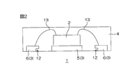
- FIG. 2 is a schematic cross-sectional view of the semiconductor device shown in FIG. 1 taken along the cutting line II-II.
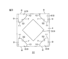
- FIG. 3 is a bottom view of the semiconductor device according to the second embodiment of the present invention.
- FIG. 4 is a bottom view of a semiconductor device according to the third embodiment of the present invention.
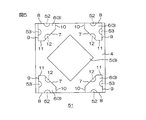
- FIG. 5 is a bottom view of a semiconductor device according to the fourth embodiment of the present invention.
- FIG. 6 is a bottom view of a semiconductor device according to the fifth embodiment of the present invention.
- FIG. 7 is a bottom view of a semiconductor device according to the sixth embodiment of the present invention.
- FIG. 1 is a bottom view of the semiconductor device according to the first embodiment of the present invention.
- FIG. 2 is a schematic cross-sectional view of the semiconductor device shown in FIG. 1 taken along the cutting line II-II.
- the semiconductor device 1 has a structure in which a semiconductor chip 2 is sealed with a resin package 4 together with a lead frame 3.
- the outer shape of the semiconductor device 1 has a flat rectangular parallelepiped shape (in this embodiment, a hexahedron having a square shape in plan view).
- the lead frame 3 is formed by punching a metal thin plate (for example, a copper thin plate), and includes an island 5 and four leads 6 disposed around the island 5.
- the island 5 has a rectangular shape in plan view (in this embodiment, a square shape in plan view).
- the lower surface of the island 5 is exposed on the back surface of the resin package 4.
- the leads 6 are disposed at portions facing the four sides of the island 5 in a bottom view.
- Each lead 6 is formed in a trapezoidal shape when viewed from the bottom. More specifically, each lead 6 is orthogonal to the side 7 parallel to the opposite side of the island 5, the side 8 extending on the side surface of the resin package 4, and the side 8 in plan view. It is formed in a shape having sides 9 extending in parallel with the side surfaces and sides 10 and 11 connecting the sides 7 and 8 and 9, respectively.
- Each lead 6 is formed with a recess 12 that is recessed from the lower surface (exposed surface) side of the lead 6 and is open on the side surface facing the island 5, that is, the side surface having the side 7 in a bottom view.
- the material of the resin package 4 enters the recess 12.
- the recess 12 can be formed by, for example, chemical etching or crushing.
- the lower surface of each lead 6 is exposed on the back surface of the resin package 4 except for the recess 12, and functions as an external terminal for connection to a wiring board (not shown). Further, the side surface having the side 8 of each lead 6 is exposed at the side surface of the resin package 4.
- the semiconductor chip 2 is bonded (die bonded) to the island 5 via a conductive bonding agent with the surface (device forming surface) on the side where the functional elements are formed facing upward.
- a pad (not shown) is formed on the surface of the semiconductor chip 2 so as to correspond to each lead 6 by exposing a part of the wiring layer from the surface protective film.
- One end of a bonding wire 13 is bonded to each pad.
- the other end of the bonding wire 13 is bonded to the upper surface of a relatively thick portion (portion where the recess 12 is not formed) in each lead 6. Thereby, the semiconductor chip 2 is electrically connected to the lead 6 via the bonding wire 13.
- each lead 6 is formed with a recess 12 which is recessed from the lower surface side and is opened on the side surface having the side 7. Since the material of the resin package 4 enters the recess 12, the portion where the recess 12 of each lead 6 is formed is sandwiched between the upper and lower sides of the resin package 4. Thereby, the joint strength between each lead 6 and the resin package 4 can be improved. As a result, it is possible to prevent the lead 6 from falling off the resin package 4.
- FIG. 3 is a bottom view of the semiconductor device according to the second embodiment of the present invention.
- parts corresponding to the parts shown in FIG. 1 are denoted by the same reference numerals as those given to the respective parts. In the following description, only the differences between the configuration shown in FIG. 3 and the configuration shown in FIG. 1 will be described, and the description of each part given the same reference numeral will be omitted.
- each lead 6 is formed with a concave portion 32 having a triangular shape as viewed from the bottom, which is recessed from the lower surface side and is opened on the side surface having the side 7.
- the material of the resin package 4 enters the recess 32.
- the recess 32 can be formed by, for example, chemical etching or crushing. Even in this configuration, the bonding strength between each lead 6 and the resin package 4 can be improved. As a result, it is possible to prevent the lead 6 from falling off the resin package 4.
- FIG. 4 is a bottom view of a semiconductor device according to the third embodiment of the present invention.
- parts corresponding to those shown in FIG. 1 are denoted by the same reference numerals as those given to the respective parts.
- a concave groove 42 that is recessed from the lower surface side of each lead 6 is formed in a portion having the side 8 in each lead 6 over the entire width along the side 8.
- FIG. 5 is a bottom view of a semiconductor device according to the fourth embodiment of the present invention.
- parts corresponding to the respective parts shown in FIG. 1 are denoted by the same reference numerals as those given to the respective parts.
- the description of each part given the same reference numeral will be omitted.
- each lead 6 is formed with recesses 12, 52, 53 that are recessed from the lower surface side and are opened on the side surfaces having the sides 7, 8, 9, and are semicircular when viewed from the bottom. Yes. According to this configuration, since the material of the resin package 4 enters the recesses 12, 52, and 53, it is possible to further improve the bonding strength between the leads 6 and the resin package 4.
- FIG. 6 is a bottom view of a semiconductor device according to the fifth embodiment of the present invention.
- parts corresponding to the parts shown in FIG. 1 are denoted by the same reference numerals as those given to the respective parts.
- each lead 6 is formed with a concave part 62 having a semicircular shape in a bottom view and having a size larger than the concave part 12 shown in FIG.
- the recess 62 is recessed from the lower surface side and is open on the side surface having the side 7.
- the area of the recess 62 in the bottom view is about 1 ⁇ 2 of the total area of the lower surface of the lead 6.
- FIG. 7 is a bottom view of a semiconductor device according to the sixth embodiment of the present invention.
- parts corresponding to the parts shown in FIG. 1 are denoted by the same reference numerals as those given to the respective parts. In the following description, only the differences between the configuration shown in FIG. 7 and the configuration shown in FIG. 1 will be described, and the description of each part given the same reference numeral will be omitted.
- groove-like recesses 72 are formed in the island 5, which are recessed from the lower surface side and extend along two diagonal lines of the island 5 in a bottom view.
- the material of the resin package 4 enters the recess 72.
- the recess 72 can be formed by, for example, chemical etching or crushing. Since the material of the resin package 4 enters the recess 72, the portion of the island 5 where the recess 72 is formed is sandwiched by the resin package 4 from both the upper and lower sides. Thereby, the joint strength between the island 5 and the resin package 4 can be improved. As a result, it is possible to prevent the island 5 from falling off the resin package 4.
- first to sixth embodiments of the present invention have been described above, the first to sixth embodiments may be implemented in appropriate combination.
- first embodiment and the fourth embodiment one or two of the three recesses 12, 52, 53 shown in FIG. May be formed in a right triangle shape in a bottom view.
- second embodiment and the third embodiment a concave portion 32 having a right triangle shape in a bottom view shown in FIG. 3 and a concave groove 42 shown in FIG. 4 are formed in each lead 6. It may be.
- SYMBOLS 1 ... Semiconductor device, 2 ... Semiconductor chip, 4 ... Resin package, 5 ... Island, 6 ... Lead, 12 ... Recessed part, 13 ... Bonding wire, 31 ... Semiconductor device, 32... Recessed portion, 41... Semiconductor device, 42... Recessed groove, 51... Semiconductor device, 52... Recessed portion, 53. ... Recesses
Landscapes
- Structures Or Materials For Encapsulating Or Coating Semiconductor Devices Or Solid State Devices (AREA)
- Engineering & Computer Science (AREA)
- Microelectronics & Electronic Packaging (AREA)
- Physics & Mathematics (AREA)
- Geometry (AREA)
- Lead Frames For Integrated Circuits (AREA)
Abstract
Description
ノンリードパッケージを採用した半導体装置は、半導体チップをリードフレームとともに樹脂パッケージで封止した構造を有している。リードフレームは、金属薄板を打ち抜くことにより形成され、アイランドと、このアイランドの周囲に配置される複数のリードとを備えている。半導体チップは、アイランドの上面にダイボンディングされており、その表面と各リードの上面との間に架設されるボンディングワイヤにより、各リードと電気的に接続されている。そして、アイランドおよび各リードの下面は、樹脂パッケージの裏面において露出している。
そこで、本発明の目的は、リードと樹脂パッケージとの接合強度の向上を図ることができる、表面実装型の半導体装置を提供することである。
そして、リードには、その下面側から窪み、側面において開放される凹部が形成されている。この凹部に樹脂パッケージの材料が入り込むことにより、リードの周縁部の一部は、その上下両側から樹脂パッケージに挟持される。これにより、リードと樹脂パッケージとの接合強度の向上を図ることができる。その結果、樹脂パッケージからのリードの脱落を防止することができる。
たとえば、リードの側面が樹脂パッケージの側面で露出する構成の場合に、凹部がその露出する側面で開放されるように形成されると、樹脂パッケージの形成のための成形金型により凹部が閉塞され、樹脂パッケージの材料が凹部に入り込まないおそれがある。
また、前記アイランドは、底面視で四角形状をなし、リードは、底面視で、アイランドの四辺とそれぞれ対向する部分に配置され、その対向する辺と平行な辺を有する形状に形成されていてもよい。この場合、各リードにおけるアイランドの各辺と対向する辺を有する側面で凹部が開放されていることが好ましい。これにより、樹脂パッケージの材料を各リードの凹部に確実に入り込ませることができるので、各リードと樹脂パッケージとの接合強度を確実に向上させることができる。
図1は、本発明の第1の実施形態に係る半導体装置の底面図である。図2は、図1に示す半導体装置を切断線II-IIで切断したときの模式的な断面図である。
半導体装置1は、半導体チップ2をリードフレーム3とともに樹脂パッケージ4で封止した構造を有している。半導体装置1の外形は、扁平な直方体形状(この実施形態では、平面視正方形状の6面体)をなしている。
アイランド5は、平面視四角形状(この実施形態では、平面視正方形状)をなしている。アイランド5の下面は、樹脂パッケージ4の裏面で露出している。
リード6は、底面視で、アイランド5の四辺とそれぞれ対向する部分に配置されている。各リード6は、底面視台形状に形成されている。より具体的には、各リード6は、平面視で、アイランド5の対向する辺と平行な辺7と、樹脂パッケージ4の側面上を延びる辺8と、辺8と直交し、樹脂パッケージ4の側面と平行に延びる辺9と、辺7と辺8,9とをそれぞれ接続する辺10,11とを有する形状に形成されている。
そして、各リード6の下面は、凹部12を除いて、樹脂パッケージ4の裏面で露出し、配線基板(図示せず)との接続のための外部端子として機能する。また、各リード6の辺8を有する側面は、樹脂パッケージ4の側面で露出している。
そして、各リード6には、その下面側から窪み、辺7を有する側面において開放される凹部12が形成されている。この凹部12に樹脂パッケージ4の材料が入り込んでいることにより、各リード6の凹部12が形成されている部分は、その上下両側から樹脂パッケージ4に挟持されている。これにより、各リード6と樹脂パッケージ4との接合強度の向上を図ることができる。その結果、樹脂パッケージ4からのリード6の脱落を防止することができる。
また、凹部12が底面視半円形状に形成されているので、その円弧のあらゆる半径方向におけるリード6と樹脂パッケージ4との接合強度を増すことができる。
図3は、本発明の第2の実施形態に係る半導体装置の底面図である。図3において、図1に示す各部に相当する部分には、それらの各部に付した参照符号と同一の参照符号を付している。そして、以下では、図3に示す構成について、図1に示す構成との相違点のみを説明し、同一の参照符号を付した各部の説明を省略する。
この構成においても、各リード6と樹脂パッケージ4との接合強度の向上を図ることができる。その結果、樹脂パッケージ4からのリード6の脱落を防止することができる。
図4に示す半導体装置41では、各リード6における辺8を有する部分に、その辺8に沿う方向の全幅にわたって、各リード6の下面側から窪む凹溝42が形成されている。
図5は、本発明の第4の実施形態に係る半導体装置の底面図である。図5において、図1に示す各部に相当する部分には、それらの各部に付した参照符号と同一の参照符号を付している。そして、以下では、図5に示す構成について、図1に示す構成との相違点のみを説明し、同一の参照符号を付した各部の説明を省略する。
この構成によれば、凹部12,52,53に樹脂パッケージ4の材料が入り込むので、各リード6と樹脂パッケージ4との接合強度のさらなる向上を図ることができる。
図6に示す半導体装置61では、各リード6に、図1に示す凹部12よりも大きいサイズの底面視半円形状の凹部62が形成されている。凹部62は、その下面側から窪み、辺7を有する側面において開放されている。そして、凹部62の底面視における面積は、リード6の下面の全面積の約1/2である。
図7は、本発明の第6の実施形態に係る半導体装置の底面図である。図7において、図1に示す各部に相当する部分には、それらの各部に付した参照符号と同一の参照符号を付している。そして、以下では、図7に示す構成について、図1に示す構成との相違点のみを説明し、同一の参照符号を付した各部の説明を省略する。
凹部72に樹脂パッケージ4の材料が入り込んでいることにより、アイランド5の凹部72が形成されている部分は、その上下両側から樹脂パッケージ4に挟持されている。これにより、アイランド5と樹脂パッケージ4との接合強度の向上を図ることができる。その結果、樹脂パッケージ4からのアイランド5の脱落を防止することができる。
本出願は、2008年12月22日に日本国特許庁に提出された特願2008-326113号に対応しており、この出願の全開示はここに引用により組み込まれるものとする。
Claims (6)
- 半導体チップと、
前記半導体チップが上面に接合されるアイランドと、
前記アイランドの周囲に配置されるリードと、
前記半導体チップの表面と前記リードの上面との間に架設されるボンディングワイヤと、
前記半導体チップ、前記アイランド、前記リードおよび前記ボンディングワイヤを一括して封止する樹脂パッケージとを含み、
前記アイランドの下面および前記リードの下面が前記樹脂パッケージの裏面で露出しており、
前記リードに、下面側から窪み、その側面において開放される凹部が形成されている、半導体装置。 - 前記凹部は、底面視で円弧状をなす部分を有している、請求項1に記載の半導体装置。
- 前記凹部は、前記リードにおける前記アイランドと対向する側面で開放されている、請求項1または2に記載の半導体装置。
- 前記アイランドは、底面視で四角形状をなし、
前記リードは、底面視で、前記アイランドの四辺とそれぞれ対向する部分に配置され、その対向する辺と平行な辺を有する形状に形成されている、請求項1~3のいずれか一項に記載の半導体装置。 - 前記凹部の底面視における面積が前記リードの下面の全面積の1/2以下である、請求項1~4のいずれか一項に記載の半導体装置。
- 前記リードは、前記樹脂パッケージの側面で露出する側面を有し、
前記リードにおけるその露出する側面に沿う部分に、当該側面に沿う方向における全幅にわたって、前記リードの下面側から窪む凹溝が形成されている、請求項1~5のいずれか一項に記載の半導体装置。
Priority Applications (9)
| Application Number | Priority Date | Filing Date | Title |
|---|---|---|---|
| US13/141,222 US8502359B2 (en) | 2008-12-22 | 2009-12-02 | Semiconductor device |
| CN2009901006313U CN202285233U (zh) | 2008-12-22 | 2009-12-02 | 半导体装置 |
| US13/930,670 US8742552B2 (en) | 2008-12-22 | 2013-06-28 | Semiconductor device |
| US14/257,217 US9035436B2 (en) | 2008-12-22 | 2014-04-21 | Semiconductor device |
| US14/637,565 US9337128B2 (en) | 2008-12-22 | 2015-03-04 | Semiconductor device |
| US15/093,825 US9607932B2 (en) | 2008-12-22 | 2016-04-08 | Semiconductor device |
| US15/449,117 US9887150B2 (en) | 2008-12-22 | 2017-03-03 | Semiconductor device |
| US15/629,243 US9793195B1 (en) | 2008-12-22 | 2017-06-21 | Semiconductor device |
| US15/856,021 US10014241B2 (en) | 2008-12-22 | 2017-12-27 | Semiconductor device |
Applications Claiming Priority (2)
| Application Number | Priority Date | Filing Date | Title |
|---|---|---|---|
| JP2008326113A JP5649277B2 (ja) | 2008-12-22 | 2008-12-22 | 半導体装置 |
| JP2008-326113 | 2008-12-22 |
Related Child Applications (2)
| Application Number | Title | Priority Date | Filing Date |
|---|---|---|---|
| US13/141,222 A-371-Of-International US8502359B2 (en) | 2008-12-22 | 2009-12-02 | Semiconductor device |
| US13/930,670 Division US8742552B2 (en) | 2008-12-22 | 2013-06-28 | Semiconductor device |
Publications (1)
| Publication Number | Publication Date |
|---|---|
| WO2010073497A1 true WO2010073497A1 (ja) | 2010-07-01 |
Family
ID=42287156
Family Applications (1)
| Application Number | Title | Priority Date | Filing Date |
|---|---|---|---|
| PCT/JP2009/006548 Ceased WO2010073497A1 (ja) | 2008-12-22 | 2009-12-02 | 半導体装置 |
Country Status (5)
| Country | Link |
|---|---|
| US (8) | US8502359B2 (ja) |
| JP (1) | JP5649277B2 (ja) |
| KR (1) | KR101647863B1 (ja) |
| CN (1) | CN202285233U (ja) |
| WO (1) | WO2010073497A1 (ja) |
Families Citing this family (8)
| Publication number | Priority date | Publication date | Assignee | Title |
|---|---|---|---|---|
| JP5649277B2 (ja) | 2008-12-22 | 2015-01-07 | ローム株式会社 | 半導体装置 |
| US9530167B2 (en) * | 2011-08-12 | 2016-12-27 | Facebook, Inc. | Coefficients attribution for different objects based on natural language processing |
| US9269690B2 (en) | 2013-12-06 | 2016-02-23 | Nxp B.V. | Packaged semiconductor device with interior polygonal pads |
| JP6857035B2 (ja) * | 2017-01-12 | 2021-04-14 | ローム株式会社 | 半導体装置 |
| US10535812B2 (en) * | 2017-09-04 | 2020-01-14 | Rohm Co., Ltd. | Semiconductor device |
| JP6652117B2 (ja) * | 2017-11-29 | 2020-02-19 | 日亜化学工業株式会社 | 樹脂パッケージおよび発光装置 |
| US11448311B2 (en) | 2018-01-11 | 2022-09-20 | Textron, Inc. | Off-highway recreational vehicle |
| CN108807329A (zh) * | 2018-05-02 | 2018-11-13 | 泰州友润电子科技股份有限公司 | 一种便于封装加工的多载型引线框架 |
Citations (2)
| Publication number | Priority date | Publication date | Assignee | Title |
|---|---|---|---|---|
| JP2003218284A (ja) * | 2002-01-22 | 2003-07-31 | Yamaha Corp | 半導体素子及びその製造方法 |
| JP2005150629A (ja) * | 2003-11-19 | 2005-06-09 | Rohm Co Ltd | リードフレームの製造方法およびそれを用いた半導体装置の製造方法、ならびにリードフレームおよびそれを用いた半導体装置 |
Family Cites Families (13)
| Publication number | Priority date | Publication date | Assignee | Title |
|---|---|---|---|---|
| CH686325A5 (de) * | 1992-11-27 | 1996-02-29 | Esec Sempac Sa | Elektronikmodul und Chip-Karte. |
| JPH08222663A (ja) | 1995-02-13 | 1996-08-30 | Calsonic Corp | ヒートシンク |
| JPH08222683A (ja) * | 1995-02-17 | 1996-08-30 | Hitachi Cable Ltd | 半導体装置用リードフレームおよび半導体装置 |
| JP4390317B2 (ja) * | 1999-07-02 | 2009-12-24 | 株式会社ルネサステクノロジ | 樹脂封止型半導体パッケージ |
| TW543172B (en) | 2001-04-13 | 2003-07-21 | Yamaha Corp | Semiconductor device and package, and method of manufacture therefor |
| US6524886B2 (en) * | 2001-05-24 | 2003-02-25 | Advanced Semiconductor Engineering Inc. | Method of making leadless semiconductor package |
| TWI338358B (en) | 2003-11-19 | 2011-03-01 | Rohm Co Ltd | Method of fabricating lead frame and method of fabricating semiconductor device using the same, and lead frame and semiconductor device using the same |
| US6984878B2 (en) * | 2004-05-24 | 2006-01-10 | Advanced Semiconductor Engineering, Inc. | Leadless leadframe with an improved die pad for mold locking |
| JP4980600B2 (ja) * | 2005-09-27 | 2012-07-18 | 旭化成エレクトロニクス株式会社 | 磁気センサ |
| US7741704B2 (en) * | 2006-10-18 | 2010-06-22 | Texas Instruments Incorporated | Leadframe and mold compound interlock in packaged semiconductor device |
| US7821113B2 (en) * | 2008-06-03 | 2010-10-26 | Texas Instruments Incorporated | Leadframe having delamination resistant die pad |
| JP5649277B2 (ja) * | 2008-12-22 | 2015-01-07 | ローム株式会社 | 半導体装置 |
| JP5220714B2 (ja) * | 2009-09-18 | 2013-06-26 | セイコーインスツル株式会社 | 樹脂封止型半導体装置及びその製造方法 |
-
2008
- 2008-12-22 JP JP2008326113A patent/JP5649277B2/ja active Active
-
2009
- 2009-12-02 WO PCT/JP2009/006548 patent/WO2010073497A1/ja not_active Ceased
- 2009-12-02 CN CN2009901006313U patent/CN202285233U/zh not_active Expired - Lifetime
- 2009-12-02 US US13/141,222 patent/US8502359B2/en active Active
- 2009-12-02 KR KR1020117017108A patent/KR101647863B1/ko active Active
-
2013
- 2013-06-28 US US13/930,670 patent/US8742552B2/en active Active
-
2014
- 2014-04-21 US US14/257,217 patent/US9035436B2/en active Active
-
2015
- 2015-03-04 US US14/637,565 patent/US9337128B2/en active Active
-
2016
- 2016-04-08 US US15/093,825 patent/US9607932B2/en active Active
-
2017
- 2017-03-03 US US15/449,117 patent/US9887150B2/en active Active
- 2017-06-21 US US15/629,243 patent/US9793195B1/en active Active
- 2017-12-27 US US15/856,021 patent/US10014241B2/en active Active
Patent Citations (2)
| Publication number | Priority date | Publication date | Assignee | Title |
|---|---|---|---|---|
| JP2003218284A (ja) * | 2002-01-22 | 2003-07-31 | Yamaha Corp | 半導体素子及びその製造方法 |
| JP2005150629A (ja) * | 2003-11-19 | 2005-06-09 | Rohm Co Ltd | リードフレームの製造方法およびそれを用いた半導体装置の製造方法、ならびにリードフレームおよびそれを用いた半導体装置 |
Also Published As
| Publication number | Publication date |
|---|---|
| US9793195B1 (en) | 2017-10-17 |
| US20180122726A1 (en) | 2018-05-03 |
| US20170287817A1 (en) | 2017-10-05 |
| US20120018896A1 (en) | 2012-01-26 |
| CN202285233U (zh) | 2012-06-27 |
| US20130285250A1 (en) | 2013-10-31 |
| JP2010147421A (ja) | 2010-07-01 |
| US9887150B2 (en) | 2018-02-06 |
| US20140225243A1 (en) | 2014-08-14 |
| US9337128B2 (en) | 2016-05-10 |
| US9607932B2 (en) | 2017-03-28 |
| KR20110102917A (ko) | 2011-09-19 |
| US20150179554A1 (en) | 2015-06-25 |
| US8742552B2 (en) | 2014-06-03 |
| US20160225700A1 (en) | 2016-08-04 |
| JP5649277B2 (ja) | 2015-01-07 |
| US9035436B2 (en) | 2015-05-19 |
| US10014241B2 (en) | 2018-07-03 |
| US8502359B2 (en) | 2013-08-06 |
| US20170179006A1 (en) | 2017-06-22 |
| KR101647863B1 (ko) | 2016-08-11 |
Similar Documents
| Publication | Publication Date | Title |
|---|---|---|
| JP5572622B2 (ja) | 半導体装置 | |
| WO2010073497A1 (ja) | 半導体装置 | |
| JP6092645B2 (ja) | 半導体装置 | |
| CN100474579C (zh) | 电路装置 | |
| CN101188227A (zh) | 半导体装置 | |
| JP2004047715A (ja) | 半導体接続中継部材及び半導体装置 | |
| CN100524722C (zh) | 无外引脚导线架的封装结构 | |
| US9293399B2 (en) | Semiconductor device and electronic unit provided with the same | |
| JP5283946B2 (ja) | 半導体装置およびそれに用いる複合リードフレーム | |
| JP2007201251A (ja) | 半導体パッケージ及び半導体パッケージの製造方法 | |
| JP2009004475A (ja) | リードフレームおよびそれを用いた半導体装置 | |
| JP2006339317A (ja) | 表面実装型半導体装置 |
Legal Events
| Date | Code | Title | Description |
|---|---|---|---|
| WWE | Wipo information: entry into national phase |
Ref document number: 200990100631.3 Country of ref document: CN |
|
| 121 | Ep: the epo has been informed by wipo that ep was designated in this application |
Ref document number: 09834312 Country of ref document: EP Kind code of ref document: A1 |
|
| NENP | Non-entry into the national phase |
Ref country code: DE |
|
| ENP | Entry into the national phase |
Ref document number: 20117017108 Country of ref document: KR Kind code of ref document: A |
|
| WWE | Wipo information: entry into national phase |
Ref document number: 13141222 Country of ref document: US |
|
| 122 | Ep: pct application non-entry in european phase |
Ref document number: 09834312 Country of ref document: EP Kind code of ref document: A1 |