WO2010070948A1 - 液晶表示用パネル及び液晶表示装置 - Google Patents
液晶表示用パネル及び液晶表示装置 Download PDFInfo
- Publication number
- WO2010070948A1 WO2010070948A1 PCT/JP2009/063292 JP2009063292W WO2010070948A1 WO 2010070948 A1 WO2010070948 A1 WO 2010070948A1 JP 2009063292 W JP2009063292 W JP 2009063292W WO 2010070948 A1 WO2010070948 A1 WO 2010070948A1
- Authority
- WO
- WIPO (PCT)
- Prior art keywords
- film
- liquid crystal
- crystal display
- region
- external connection
- Prior art date
- Legal status (The legal status is an assumption and is not a legal conclusion. Google has not performed a legal analysis and makes no representation as to the accuracy of the status listed.)
- Ceased
Links
Images





Classifications
-
- G—PHYSICS
- G02—OPTICS
- G02F—OPTICAL DEVICES OR ARRANGEMENTS FOR THE CONTROL OF LIGHT BY MODIFICATION OF THE OPTICAL PROPERTIES OF THE MEDIA OF THE ELEMENTS INVOLVED THEREIN; NON-LINEAR OPTICS; FREQUENCY-CHANGING OF LIGHT; OPTICAL LOGIC ELEMENTS; OPTICAL ANALOGUE/DIGITAL CONVERTERS
- G02F1/00—Devices or arrangements for the control of the intensity, colour, phase, polarisation or direction of light arriving from an independent light source, e.g. switching, gating or modulating; Non-linear optics
- G02F1/01—Devices or arrangements for the control of the intensity, colour, phase, polarisation or direction of light arriving from an independent light source, e.g. switching, gating or modulating; Non-linear optics for the control of the intensity, phase, polarisation or colour
- G02F1/13—Devices or arrangements for the control of the intensity, colour, phase, polarisation or direction of light arriving from an independent light source, e.g. switching, gating or modulating; Non-linear optics for the control of the intensity, phase, polarisation or colour based on liquid crystals, e.g. single liquid crystal display cells
- G02F1/133—Constructional arrangements; Operation of liquid crystal cells; Circuit arrangements
- G02F1/1333—Constructional arrangements; Manufacturing methods
- G02F1/1339—Gaskets; Spacers; Sealing of cells
- G02F1/13394—Gaskets; Spacers; Sealing of cells spacers regularly patterned on the cell subtrate, e.g. walls, pillars
-
- G—PHYSICS
- G02—OPTICS
- G02F—OPTICAL DEVICES OR ARRANGEMENTS FOR THE CONTROL OF LIGHT BY MODIFICATION OF THE OPTICAL PROPERTIES OF THE MEDIA OF THE ELEMENTS INVOLVED THEREIN; NON-LINEAR OPTICS; FREQUENCY-CHANGING OF LIGHT; OPTICAL LOGIC ELEMENTS; OPTICAL ANALOGUE/DIGITAL CONVERTERS
- G02F1/00—Devices or arrangements for the control of the intensity, colour, phase, polarisation or direction of light arriving from an independent light source, e.g. switching, gating or modulating; Non-linear optics
- G02F1/01—Devices or arrangements for the control of the intensity, colour, phase, polarisation or direction of light arriving from an independent light source, e.g. switching, gating or modulating; Non-linear optics for the control of the intensity, phase, polarisation or colour
- G02F1/13—Devices or arrangements for the control of the intensity, colour, phase, polarisation or direction of light arriving from an independent light source, e.g. switching, gating or modulating; Non-linear optics for the control of the intensity, phase, polarisation or colour based on liquid crystals, e.g. single liquid crystal display cells
- G02F1/133—Constructional arrangements; Operation of liquid crystal cells; Circuit arrangements
- G02F1/1333—Constructional arrangements; Manufacturing methods
- G02F1/133388—Constructional arrangements; Manufacturing methods with constructional differences between the display region and the peripheral region
Definitions
- the present invention relates to a liquid crystal display panel and a liquid crystal display device. More specifically, the present invention relates to a liquid crystal display panel and a liquid crystal display device that can be suitably used for a liquid crystal display device in which external components are mounted on external connection terminal portions.
- the liquid crystal display device is a thin and low power consumption display device, it is an OA device such as a personal computer, a portable information terminal device such as an electronic notebook or a mobile phone, or a monitor of a camera-integrated VTR. It is widely used in products such as these, and has been actively developed to meet the requirements for adapting to the diversified information society.
- a liquid crystal display panel usually has a structure in which two substrates are bonded together with a sealing material.
- a method of controlling the cell thickness by arranging a spacer in the display area is generally used, but there is still room for improvement in order to further improve the display quality.
- a terminal is provided on one substrate for connection to the outside, and an external member is connected to the terminal by an anisotropic conductive film.
- an external member a flexible printed circuit board (FPC: Flexible Printed Circuits) and COG (Chip on Glass) are mentioned, for example.
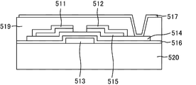
- the conventional liquid crystal display device has a source electrode 511, a drain electrode 512, a gate electrode 513, an amorphous silicon film 514, an ohmic contact layer 515, and a gate insulation on a substrate 520 in the display region.
- a thin film transistor including the film 516 is provided, and an organic insulating film 519 and a reflective electrode 517 formed over the thin film transistor are further provided.
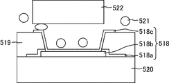
- an opening is formed in the organic insulating film 519, and the conductive films 518a, 518b and 518c are formed in the opening.
- the pad 518 is formed, and the pad 518 and the bump 522 of the COG are connected by the conductive particles 521 included in the anisotropic conductive film.
- the pad 518 and the bump 522 are not connected to each other inside the opening, and defects are likely to occur. As a result, the liquid crystal display device may not operate or may malfunction.
- a pixel including a thin film transistor is formed as a switching element in an element region which is a central portion of the substrate, and a gate input pad and a data input pad are formed in a pad region which is an outer portion of the substrate.
- An organic insulating film is formed on the entire surface of the substrate on which the thin film transistor and the pad are formed, and the organic insulating film is exposed and developed to form a concavo-convex structure on the organic insulating film for forming a bend in the reflective electrode.
- a technique is disclosed in which an organic insulating film is formed on the upper surface of the pad and a portion adjacent to the pad so as to have a small step compared to other portions (see, for example, Patent Document 1).
- the substrate of the liquid crystal display device has a signal line extending from the display area to the non-display area, and is provided with a plurality of terminals at its end to electrically connect the external circuit and the display area circuit, A flat protective film covering the terminal is formed, and a pad connected to the terminal is formed on the protective film.
- Each of the plurality of pads has a contact region and a flat contact region, and each pad is formed in the contact region. The pad is contacted with a corresponding terminal formed in the lower portion through a pad contact hole formed in the protective film, and each pad is electrically contacted with an external circuit terminal by pressure bonding through an anisotropic conductive resin in a flat contact region.
- a technique is disclosed (for example, see Patent Document 2).
- the present invention has been made in view of the above situation, and provides a liquid crystal display panel capable of suppressing cell thickness unevenness and achieving uniform display in the entire display region, and a liquid crystal display device including the same. It is intended.
- the present inventor has conducted various studies on techniques for suppressing the cell thickness unevenness of the liquid crystal display device and improving the display quality.
- the inter-substrate distance between a pair of substrates between the inner side and the outer side surrounded by the sealing material. Focusing on (distance), it was conceived that spacers were provided in both the display area and the area (terminal area) where the pads (external connection terminals) were arranged.
- the height of the member (panel constituent member) constituting the liquid crystal display panel is the inner side of the sealing material. And outside.
- the height of the panel constituent member in the terminal area is different from the height of the panel constituent member in the display area. For this reason, it has been found that there is a difference in the distance between the substrates between the inside and the outside of the sealing material, causing display unevenness. Therefore, spacers are arranged inside and outside the region surrounded by the sealing material, and the thickness of the panel constituent members arranged in the region overlapping with the spacer of the thin film transistor substrate is set so that the inside and outside of the region surrounded by the sealing material are It has been found that by using substantially the same liquid crystal display panel, the display unevenness caused by the cell thickness unevenness can be suppressed and uniform display can be performed over the entire display area, and the above problems can be solved brilliantly. The present invention has been reached.
- the present invention is a liquid crystal display panel in which a thin film transistor substrate and a counter substrate facing the thin film transistor substrate (thin film transistor substrate) are bonded together with a sealing material, and a liquid crystal layer is sandwiched inside a region surrounded by the sealing material.
- a liquid crystal display panel In the liquid crystal display panel, spacers are disposed inside and outside the region surrounded by the sealing material.
- the thickness of the panel constituent member disposed in the region overlapping the spacer is surrounded by the sealing material.
- the liquid crystal display panel is substantially the same between the inside and the outside of the region.
- the liquid crystal display panel of the present invention is a thin film transistor (TFT) substrate and a counter substrate opposite to each other, which are bonded together with a sealing material, and a liquid crystal layer is sandwiched inside a region surrounded by the sealing material. is there.
- the TFT substrate is a substrate provided with a panel constituent member including a TFT, an external connection terminal and the like on a substrate such as a glass substrate.
- a preferable form of the TFT substrate for example, a form having a display area inside the area surrounded by the sealing material and a terminal area in which the external connection terminals are arranged outside is mentioned.
- the counter substrate include, but are not limited to, a color filter (CF) substrate provided with a color filter or the like on a glass substrate.
- CF color filter
- the sealing material is disposed so as to surround the display region, and is usually disposed on the outer edge portion of the TFT substrate and the counter substrate, and the two substrates are bonded together. Then, a liquid crystal material is sealed between the pair of substrates bonded with the sealing material, and a display region is formed inside the sealing material.
- spacers are arranged on the inner side and the outer side of the region surrounded by the sealing material.
- the spacer is disposed both in the region surrounded by the sealing material and on the outside of the sealing material.
- the spacer is used to make the distance between a pair of substrates (inter-substrate distance) uniform.
- the kind of the spacer is not particularly limited, and may be a particulate spacer such as a bead or a columnar spacer.
- the columnar spacer is molded, for example, by patterning a resin such as a curable resin.
- a photospacer formed from a photocurable resin and beads for the spacer are preferably used.
- the spacer may be provided on the TFT substrate or may be provided on the counter substrate. Further, the height (thickness) of the spacer is not particularly limited. However, the spacer is usually used to make the thickness of the liquid crystal layer uniform. For this reason, the height of the spacer is usually preferably approximately the same as the thickness of the liquid crystal layer.
- the area of the spacer when seen in a plan view may be adjusted as appropriate according to the size of the liquid crystal display panel and the size of the pixel, but is preferably 10 to 5000 ⁇ m 2 .
- the TFT substrate is one in which panel constituent members are arranged inside and outside a region surrounded by a sealing material.
- the panel constituent member is disposed both in the region surrounded by the sealing material and on the outside of the sealing material. It does not specifically limit as a form of the said panel structural member, A various form is mentioned.
- the panel constituent member disposed inside the region surrounded by the sealing material include a TFT composed of a gate electrode, a source electrode, a drain electrode, a gate insulating film, a semiconductor layer, a planarization film, an interlayer film, and the like.
- members formed on a substrate such as a pixel electrode, an auxiliary capacitance electrode, and an alignment film.
- an external connection terminal for transmitting a signal from the outside, a wiring for transmitting a signal to the external connection terminal, a planarization film, and the like.
- various circuits such as a driver circuit, a power supply circuit, and an electrostatic discharge (ESD) protection circuit are configured.
- ESD electrostatic discharge
- panel constituent member refers to an aggregate of members provided on the TFT substrate and constituting the liquid crystal display panel.
- the thickness of the panel constituent member disposed in the region overlapping with the spacer is substantially equal between the inside and the outside of the region surrounded by the sealing material.
- region which overlaps with the said spacer becomes substantially equal inside and the outer side of the area
- the sealing material when the distance between the substrates on the inner side (for example, the display region) and the outer side (for example, the terminal region) of the sealing material is different, stress due to the gap difference of the distance between the substrates occurs when the substrates are bonded together. There is a possibility that unevenness of the cell thickness occurs in the vicinity of the sealing material in the terminal region, and the display quality is deteriorated.
- substantially equal may be equal to a level that can sufficiently improve display quality by suppressing cell thickness unevenness.
- the outer side of the sealing material for example, a terminal region
- the thickness of the panel constituent member in the region overlapping with the spacer disposed in the region is within ⁇ 15%, that is, 85 to 115% of the thickness of the region overlapping with the spacer disposed inside the sealing material. Including some. With such a difference, display unevenness due to the difference in distance between the substrates can be sufficiently suppressed, and a liquid crystal display panel with excellent display quality can be obtained.
- the thickness of the panel constituent member in the region overlapping with the spacer may be substantially unequal between the inner side and the outer side of the sealing material, for example, each of the inner side and the outer side of the region surrounded by the sealing material
- the thickness of the panel constituent member in the region overlapping with at least one of the spacers disposed on the inner side of the sealing material is disposed on the outer side of the sealing material.
- the configuration of the liquid crystal display panel of the present invention is not particularly limited as long as such components are formed as essential, and other components may or may not be included. is not.
- the total height of the members disposed on the counter substrate for example, the color filter substrate
- a reflective film may be disposed in the reflective display area, or a member for adjusting the thickness of the liquid crystal layer in the reflective display area (For example, a white color filter) may be provided so as to have a thickness that is approximately 1 ⁇ 2 of the thickness of the liquid crystal layer in the transmissive display region.
- the thin film transistor substrate has a structure in which an external connection terminal is provided outside a region surrounded by a sealing material, and a planarizing film is disposed in a region overlapping with inner and outer spacers of the region surrounded by the sealing material.
- the planarizing film is removed in at least a part of a region where the external connection terminals are arranged.
- the planarization film is formed in a region where the external connection terminal is not disposed. It is left and arranged.
- the spacers are arranged in the region where the remaining planarization film is arranged, so that the distance between the substrates can be made uniform. In this way, even in a form in which a part of the planarizing film is removed outside the region surrounded by the sealing material, in the region where the spacer is arranged, the inside and outside of the region surrounded by the sealing material
- the panel constituent members have substantially the same thickness. Therefore, it is possible to suppress the occurrence of cell thickness unevenness and improve display quality.
- the planarizing film is usually formed thicker than other members constituting the panel constituent member (for example, members constituting the TFT). Therefore, when this planarization film does not exist in the region overlapping with the spacer outside the region surrounded by the sealing material, the thickness (height from the glass substrate or the like) of the panel constituent member is different between the inner side and the outer side of the sealing material. This is a significant difference, and the distance between the substrates varies greatly between the inside and outside of the sealing material. For this reason, cell thickness nonuniformity arises and there exists a possibility that display quality may fall.
- planarizing film may be placed in place of the planarizing film in the region overlapping with the spacer, but in order to form a film having the same thickness as the planarizing film, the number of steps is increased, and productivity is increased. May decrease.
- the planarizing film is preferably a film disposed immediately below the pixel electrode.
- the pixel electrode formed immediately above the pixel electrode may have a shape reflecting the irregularities.
- the display quality may be deteriorated. Therefore, by disposing the planarizing film immediately below the pixel electrode, the pixel electrode can be made flat and display quality can be improved.
- “arranged immediately below the pixel electrode” means that the element is disposed in contact with at least a part of the lower surface of the pixel electrode.
- the flattening film is a film that is arranged to make the thickness of the panel constituent member uniform.
- the material for forming the planarizing film is not particularly limited, and examples thereof include an organic insulating film formed from an organic insulating material, a SOG (spin on glass) film formed from a methyl-containing polysiloxane (MSQ) -based material, and the like. It is done. Further, these materials may be laminated and used.
- the flattening film the upper surface of the flattening film can be made flat even when unevenness is formed by a member disposed below the flattening film.
- the planarizing film is preferably a film having a thickness of 0.5 ⁇ m or more.
- a semiconductor element such as a TFT
- irregularities of about 0.5 ⁇ m may be formed.
- the planarizing film having a thickness of 0.5 ⁇ m or more is preferable.
- the planarizing film is preferably a film having a thickness of 4 ⁇ m or less. If the film exceeds 4 ⁇ m, for example, when a contact hole is formed in the film, the area may be increased or the etching time may be increased. On the other hand, when the thickness exceeds 4 ⁇ m, when the planarizing film is formed from a photosensitive material, unevenness of the film thickness may occur during application or exposure may be insufficient.
- the end of the external connection terminal is disposed immediately below the planarization film.
- aluminum is often used as one of the conductive materials used for the external connection terminals.
- the external connection terminal includes an aluminum film, it is preferable to dispose a conductive film (for example, a titanium film) that hardly corrodes on the aluminum film so that the aluminum film is not exposed to the atmosphere. is there.
- a conductive film for example, a transparent conductive film for forming a pixel electrode
- a transparent conductive film is further patterned to cover the exposed side surface of the aluminum film and the conductive film disposed on the upper surface thereof.
- an external connection terminal since a transparent conductive film usually has a higher resistance than a conductive film such as a titanium film, an external connection terminal having a transparent conductive film disposed on the upper surface may have a high contact resistance when connected to the outside. .
- the end of the external connection terminal is arranged immediately below the planarization film, that is, the end of the external connection terminal is covered with the planarization film, thereby forming the end of the external connection terminal.
- Exposure of the conductive film that is easily corroded can be suppressed, and corrosion of the external connection terminal can be suppressed.
- Such a form is a particularly preferable form when the external connection terminal includes a conductive film which is easily corroded such as aluminum.
- the external connection terminal includes a conductive film that is susceptible to corrosion, such as aluminum, and a conductive film that is resistant to corrosion, such as a titanium alloy film such as titanium film or titanium nitride, and the top surface of the conductive film that is susceptible to corrosion corrodes. This is particularly effective in a form in which the side surface of the conductive film which is covered with a highly resistant conductive film and which is easily corroded is not covered with the conductive film resistant to corrosion.
- the external connection terminal does not include a transparent conductive film. More specifically, the external connection terminal is preferably in a form in which another conductive film is not covered with a transparent conductive film. As described above, by disposing the end portion of the conductive film which is easily corroded, such as an aluminum film, directly below the planarizing film, corrosion can be suppressed without providing a transparent conductive film. In addition, since the transparent conductive film usually has a higher resistivity than the metal film, the contact resistance increases when this is used as the conductive film constituting the surface of the external connection terminal. On the other hand, contact resistance can be reduced by adopting a form in which the upper layer of the external connection terminal is not covered with the transparent conductive film.
- the transparent conductive film is not particularly limited, and examples thereof include an indium tin oxide film and an indium zinc oxide film.
- a multilayer wiring structure in which a first conductive film, a first planarizing film, a second conductive film, and a second planarizing film are arranged in this order inside a region surrounded by a sealing material.
- the external connection terminal does not include a conductive film formed in the step of forming the second conductive film.
- a laminated film having a structure such as a molybdenum film / aluminum film is preferably used for the conductive film forming the second conductive film.
- the film disposed in the upper layer is a film that is low in water resistance compared to a titanium film or the like, such as a molybdenum film, and is susceptible to corrosion
- forming an external connection terminal using this molybdenum film Corrosion may cause problems in reliability. Therefore, by adopting a structure in which the external connection terminal does not include the conductive film formed in the step of forming the second conductive film, even if a metal material that is relatively easily corroded is used as the second conductive film material, Degradation of the characteristics of the connection terminal can be suppressed, and the reliability of the external connection terminal can be improved.
- the “conductive film formed in the process of forming the second conductive film” is a conductive film formed in the same film forming process and patterning process as the second conductive film. It is the electrically conductive film formed in the same vapor deposition process and patterning process.
- the thin film transistor substrate has the multilayer wiring structure
- the first conductive film and the second conductive film as wirings respectively
- a part of the first conductive film and a part of the second conductive film Can be arranged so as to overlap each other via the first planarization film. Therefore, the area of the region where the wiring is arranged can be reduced.
- the first conductive film can be used as a local wiring (a locally formed wiring) such as a source wiring or a drain wiring of a thin film transistor in the circuit.
- the second conductive film can be used as, for example, a power supply wiring such as a driver or a power supply circuit, a common wiring for signal wiring, or the like.
- the upper layer of the first conductive film is a titanium film
- the conductive film formed in the same process as the first conductive film is used as an external connection terminal
- the second conductive film is not used as a film constituting the external connection terminal. May be.
- the upper titanium film of the first conductive film can be used as an etching stopper.
- the first conductive film includes an aluminum film
- the aluminum at the end of the first conductive film is usually disposed under the first planarizing film, so that it is etched simultaneously with the wet etching. Can be prevented.
- a form having a wiring structure, in which the external connection terminal does not include the conductive film formed in the step of forming the first conductive film is also included.
- the first conductive film material is formed in the step of forming the first conductive film.
- the external connection terminal transmits a power and / or signal from the outside (for example, an external member such as an FPC) to a wiring provided on the thin film transistor substrate or a signal from the thin film transistor substrate to the outside. It is a terminal used for this purpose, and has conductivity.
- the configuration of the external connection terminal is not particularly limited, and may be, for example, a single-layer film made of a single-layer conductive film or a stacked film in which a plurality of conductive films are stacked.
- the external connection terminal is provided in a terminal region outside the region surrounded by the sealing material, and a planarizing film is disposed in the terminal region. Since the external connection terminal is connected to an external member, the thin film transistor substrate is flattened so that contact failure does not occur between the external connection terminal and the external member due to a step around the external connection terminal. A form in which is arranged is preferable. In order to achieve such a configuration, for example, in the vicinity of the external connection terminal (in the region where the external connection terminal is disposed and its surroundings), the planarizing film is externally attached to the bump of COG, the external connection wiring of the FPC, and the like.
- an area that is 10% or more wider than the area of the terminal of the member (area when viewed in plan) is removed. More preferably, it is a form in which an area larger by 20% or more is removed.
- the external connection terminal is connected to an external member by an anisotropic conductive film.
- the anisotropic conductive film is a film that has conductivity in the out-of-plane direction (normal direction with respect to the substrate plane) but does not have conductivity in the in-plane direction (substrate plane direction).
- each terminal of an external member and each external connection terminal can be electrically connected in a one-to-one correspondence.
- the anisotropic conductive film has adhesiveness in order to physically bond the external connection terminal and the external member.
- an anisotropic conductive film one that conducts the external connection terminal and the external member by conductive particles contained in the insulating material is suitable.
- the shape of the conductive particles is not particularly limited, and may be a cubic shape, an octahedral shape, or the like, but a spherical shape is preferable.
- the external member connected to the anisotropic conductive film is not particularly limited, and examples thereof include electronic components such as resistors, capacitors, coils, connectors, diodes, transistors; flexible printed circuit boards (FPCs) (Flexible Printed Circuits). And a chip (COG: Chip On Glass) or a resin film (COF: Chip On film) on which an integrated circuit (IC: Integrated Circuit) including circuit elements and wirings is formed.
- FPCs Flexible printed circuit boards
- COG Chip On Glass
- COF Chip On film
- IC integrated circuit
- Other examples include a printed wiring board (PWB: Printed Wiring Board), a printed circuit board (PCB: Printed Circuit Board), and a tape carrier package (TCP: Tape Carrier Package).
- PWB Printed Wiring Board
- PCB printed circuit board
- TCP Tape Carrier Package
- the external member preferably includes a conductive protrusion in a region overlapping with the external connection terminal.
- a conductive protrusion is also referred to as “external connection wiring” or “bump”.
- Such conductive protrusions are connected to the external connection terminals via the conductive particles in the anisotropic conductive film.
- the present invention is also a liquid crystal display device including the liquid crystal display panel.
- a liquid crystal display panel that can suppress the occurrence of uneven cell thickness as described above, a liquid crystal display device with excellent display quality can be obtained.
- a member such as a polarizing plate is mounted on a liquid crystal display panel.
- liquid crystal display panel of the present invention since the cell thickness unevenness can be suppressed and the display can be homogenized over the entire display region, a liquid crystal display device with higher display quality can be obtained.
- FIG. 3 is a schematic cross-sectional view illustrating the liquid crystal display panel according to Embodiment 1 and illustrates a pixel region inside a region surrounded by a sealing material. It is a cross-sectional schematic diagram which shows the liquid crystal display panel which concerns on Embodiment 1, and shows the terminal area
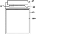
- 3 is a schematic plan view of the liquid crystal display panel according to Embodiment 1.
- FIG. FIG. 4 is a schematic plan view in which a region surrounded by a dotted line in FIG. 3 is enlarged.
- FIG. 1 is a schematic cross-sectional view illustrating the liquid crystal display panel according to Embodiment 1 and illustrates a pixel region inside a region surrounded by a sealing material. It is a cross-sectional schematic diagram which shows the liquid crystal display panel which concerns on Embodiment 1, and shows the terminal area
- 3 is a schematic plan view of the liquid crystal display panel according to Em
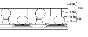
- FIG. 3 is a schematic cross-sectional view showing the liquid crystal display panel according to Embodiment 1, and shows a structure when an external connection terminal and a flexible printed circuit board (FPC) are bonded together with an anisotropic conductive film in a terminal region of the TFT substrate.
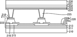
- It is a cross-sectional schematic diagram which shows the liquid crystal display panel which concerns on Embodiment 2, and shows the terminal area
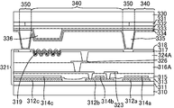
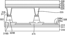
- FIG. 10 is a schematic cross-sectional view illustrating a liquid crystal display panel according to Embodiment 3 and illustrates a pixel region inside a region surrounded by a sealing material.
- FPC flexible printed circuit board
- FIG. 1 is a schematic cross-sectional view illustrating a liquid crystal display panel according to Embodiment 1, and illustrates a pixel region inside a region surrounded by a sealing material.
- FIG. 2 is a schematic cross-sectional view showing the liquid crystal display panel according to the first embodiment, and shows a terminal region outside the region surrounded by the sealing material.
- FIG. 3 is a schematic plan view of the liquid crystal display panel according to Embodiment 1
- FIG. 4 is an enlarged schematic plan view of a region surrounded by a dotted line in FIG.
- FIG. 5 is a schematic cross-sectional view illustrating the liquid crystal display panel according to the first embodiment.
- the liquid crystal display panel according to Embodiment 1 has a structure in which a TFT substrate provided with TFTs, pixel electrodes and the like and a color filter substrate provided with color filters and the like are bonded together with a sealant.
- a member for forming a plurality of liquid crystal display panels is formed on one large glass substrate, and two large glass substrates (for example, a plurality of TFT substrates are formed).
- the large glass substrate on which the members are formed and the large glass substrate on which the members constituting the plurality of color filter substrates are bonded with a sealant, and then divided into each liquid crystal display panel.
- FIGS. 1 and 2 are schematic cross-sectional views showing a form before the large glass substrate is divided into each liquid crystal display panel.
- FIGS. 3 to 5 are views after the large glass substrate is divided into each liquid crystal display panel. It is a cross-sectional schematic diagram or plane schematic diagram which shows.
- a base layer 111 in which a silicon oxynitride film having a thickness of 50 nm and a TEOS film (silicon oxide film) having a thickness of 100 nm are stacked is provided on a substrate 110, and a semiconductor layer is formed thereon.
- 112a, 112b and 112c are provided in an island shape.
- a first insulating film 113 serving as a gate insulating film is provided over the base layer 111 and the semiconductor layers 112a, 112b, and 112c.
- a gate wiring 114b and auxiliary capacitance electrodes 114a and 114c are provided on the first insulating film 113.
- the auxiliary capacitance electrodes 114a and 114c are arranged so as to overlap with the semiconductor layers 112a and 112c, respectively, and form an auxiliary capacitance.
- a laminated interlayer film 115 in which a cap film made of TEOS, a SiNx film, and a TEOS film are laminated is formed on the gate wiring 114b and the auxiliary capacitance electrodes 114a and 114c.
- a source / drain wiring 123 is formed on the laminated interlayer film 115.
- the source / drain wiring 123 has a structure in which a titanium film having a thickness of 100 nm, an aluminum film having a thickness of 350 nm, and a titanium film having a thickness of 100 nm are laminated in this order.
- the source / drain wiring 123 is connected to the semiconductor layer 112 b through a contact hole formed in the first insulating film 113 and the laminated interlayer film 115. Thereby, a TFT serving as a pixel switching element is formed.
- a planarizing film 116A which is an organic insulating film, is formed.
- a transparent conductive film 117 made of indium tin oxide is disposed on the planarizing film 116A.
- the transparent conductive film 117 is connected to the drain side of the source / drain wiring 123 through a contact hole formed in the planarizing film 116A.
- the transparent conductive film 117 functions as a pixel electrode in the display region.
- unevenness is formed in a part of the pixel region 140 of the planarizing film 116A.
- a reflective film 119 in which a 50 nm-thickness molybdenum film, a 100 nm-thickness aluminum film, and a 30 nm-thick indium zinc oxide film are stacked is disposed in the region where the unevenness is formed.
- a region where the reflective film 119 is disposed in the pixel region 140 functions as a reflective display region, and a region where the reflective film 119 is not disposed in the pixel region 140 functions as a transmissive display region.
- An alignment film 118 is disposed on the reflective film 119 and the transparent conductive film 117.
- a color filter 131 is disposed on the substrate 130.
- An overcoat layer 132 is disposed on the color filter 131.
- a white color filter 136 having a thickness of 2 ⁇ m is disposed in the reflective display region on the overcoat layer 132 (region facing the region where the reflective film 119 is disposed).
- a common electrode 133 made of indium tin oxide is disposed on the entire surface of the substrate.
- a photo spacer 135 having a height of 4 ⁇ m is disposed.
- An alignment film 134 is disposed on the common electrode 133 and the photo spacer 135. The photo spacer 135 is in contact with the alignment film 118 in the boundary region 150 through the alignment film 134.
- FIG. 2 is a schematic cross-sectional view showing the liquid crystal display panel according to the first embodiment, and shows a terminal region outside the region surrounded by the sealing material.
- FIG. 2 shows a form before the large glass substrate is divided into each liquid crystal display panel.
- FIG. 2 shows a form in which the color filter substrate and the TFT substrate face each other at the external connection terminal portion.
- the base layer 111 and the first insulating film 113 are arranged in this order on the substrate 110 in the terminal area, as in the display area.
- a conductive film 120a patterned in the same process as the gate wiring 114b is disposed on the first insulating film 113.
- a laminated film 120b patterned in the same process as the source / drain wiring 123 is disposed on the conductive film 120a.
- a transparent conductive film 120c patterned in the same process as the transparent conductive film 117 is disposed on the conductive film 120b.
- the external connection terminal 120 in which the conductive films 120 a, 120 b, and 120 c are stacked is provided on the first insulating film 113.
- a laminated interlayer film 115 is disposed in a region where the external connection terminal 120 is not disposed. However, the end of the external connection terminal 120 and the end of the laminated interlayer film 115 partially overlap.
- a planarization film 116B patterned by exposure and development processing is disposed on the laminated interlayer film 115.
- a patterned transparent conductive film 117 and an alignment film 118 are stacked on the top (upper surface) of the planarizing film 116B.
- the planarizing film 116B is provided around the external connection terminal 120, and specifically, is disposed in a region 5 to 10 ⁇ m away from the end of the external connection terminal 120.
- the color filter 131, the overcoat layer 132, and the common electrode 133 are arranged in this order on the substrate 130.
- a photo spacer 135 having a height of 4 ⁇ m is disposed on the common electrode 133.
- An alignment film 134 is disposed on the common electrode 133 and the photo spacer 135.
- the photo spacer 135 is disposed in a region facing the region where the planarizing film 116B, the transparent conductive film 117, and the alignment film 118 that are patterned so as not to overlap with the external connection terminal 120 are disposed in this order.
- the height of the panel constituent member 121 in the region facing the spacer 135 in the display region from the substrate 110 is substantially the same as the height of the panel constituent member 122 in the region facing the spacer 135 in the terminal region from the substrate 110. It becomes the same height. This is because the thickness of the members disposed below the transparent conductive film 117 is averaged by the planarization films 116A and 116B.
- the inter-substrate distance in the display region and the terminal region can be made uniform, so that occurrence of cell thickness unevenness in the display region can be suppressed. And it can be set as the liquid crystal display panel of the outstanding display quality.
- the transparent conductive film 117 and the alignment film 118 are preferably disposed on the planarizing film 116B in the terminal region from the viewpoint of making the distance between the substrates more uniform.
- the transparent conductive film 117 and the alignment film 118 are thinner than the planarization film 116B. Therefore, the distance between the substrates can be sufficiently uniformed without the transparent conductive film 117 and the alignment film 118. Therefore, the transparent conductive film 117 and the alignment film 118 may not be disposed on the planarization film 116B.
- the liquid crystal display panel according to Embodiment 1 after being separated from the large glass substrate has a sealing material 161 surrounding the display area 160.
- the sealing material 161 is disposed between the TFT substrate and the color filter substrate.
- An electronic component 162 such as a capacitor, a flexible printed circuit board (FPC) 166, and an integrated circuit (IC: Integrated Circuit) including circuit elements and wiring are formed in a terminal region outside the region surrounded by the sealant 161.
- IC integrated circuit
- COG Chip On Glass
- the external connection terminal 120 As the external connection terminal 120, the external connection terminal 120 ⁇ / b> A for connecting to the bank of the COG 167 and the external connection wiring 166 a of the FPC 166 are connected as shown in FIG. 4.
- the external connection terminal 120B is provided.
- the external connection wiring 166a and the external connection terminal 120B are electrically connected by the conductive particles 165a in the anisotropic conductive film 165.
- the COG 164 is also connected to the external connection terminal 120 ⁇ / b> A by the anisotropic conductive film 165 similarly to the FPC 166. Further, as shown in FIG.
- the planarization film 116 ⁇ / b> B is removed to such an extent that it does not overlap with the external connection wiring 166 a of the FPC 166, so that the contact failure is also suppressed. It will be.
- the planarizing film 116 ⁇ / b> B is removed so that contact failure does not occur at the connection portion with the COG 167 so as to overlap with the bumps of the COG 167.
- the external connection wiring 166a is formed over the FPC base material 166b, and the conductive particles 165a are dispersed in the insulating material 165b.
- the color filter substrate exists up to a position overlapping with the external connection terminal 120 arranged outside the sealing material 161 in the printing process of the sealing material 161 and the bonding process of the substrates. It overlaps the substrate. Thereafter, in the dividing step (terminal extraction step) for dividing the large glass substrate into each liquid crystal display panel, the area facing the external connection terminal 120 of the color filter substrate is removed, and all external devices including the external connection terminals 120A and 120B are removed. The connection terminal 120 is exposed.
- the external connection terminal 120 and the color filter substrate are arranged at positions facing each other, but in FIGS. 3 to 5 showing the post-cutting process, the external connection terminal 120 faces.
- the color filter substrate is not disposed at the position.
- the cause of the cell thickness unevenness is that a pressure difference is generated between the outer side and the inner side of the sealing material 161 during the bonding process due to the difference in density distribution of the spacer 135 between the outer side and the inner side of the sealing material 161. Accordingly, there is no particular problem even if there is no opposing spacer 135 around the external connection terminal 120 after the dividing step.
- the manufacturing method of the panel for display apparatuses which concerns on Embodiment 1 is demonstrated.
- the TFT substrate will be described. Cleaning and pre-annealing are performed on the substrate 110 as pretreatment.
- substrate 110 is not specifically limited, From a viewpoint of cost etc., a glass substrate, a resin substrate, etc. are suitable. Next, the following steps (1) to (10) are performed.
- a plasma chemical vapor deposition forming a SiON film and a SiO x film by (Plasma Enhanced Chemical Vapor Deposition PECVD) method or the like, a base layer 111 .
- the source gas for forming the SiON film include a mixed gas of monosilane (SiH 4 ), nitrous oxide gas (N 2 O), and ammonia (NH 3 ).
- the SiO x film is preferably formed by using tetraethyl orthosilicate (TEOS) gas as a source gas.
- a silicon nitride (SiN x ) film using a mixed gas of monosilane (SiH 4 ) and ammonia (NH 3 ) or the like as a source gas may be used for the base layer 111.
- amorphous silicon (a-Si) film is formed by PECVD.
- the source gas for forming the a-Si film include SiH 4 and disilane (Si 2 H 6 ). Since the a-Si film formed by the PECVD method contains hydrogen, a treatment (dehydrogenation treatment) for reducing the hydrogen concentration in the a-Si layer is performed at about 500 ° C. Thereafter, a pretreatment for applying a metal catalyst to form continuous grain boundary crystalline silicon (CG-silicon) may be performed. Subsequently, laser annealing is performed, and the a-Si film is melted, cooled, and solidified to form a p-Si film.
- CG-silicon continuous grain boundary crystalline silicon
- a heat treatment for solid phase crystallization may be performed as a pretreatment for laser annealing.
- dry etching with carbon tetrafluoride (CF 4 ) gas is performed to pattern the p-Si film, thereby forming semiconductor layers 112a, 112b, and 112c.
- CF 4 carbon tetrafluoride
- a source region, a drain region, a channel region, and the like are formed in the semiconductor layers 112a, 112b, and 112c by using an ion doping method or the like after a first insulating film formation step or a gate wiring formation step described later. To do.
- a first insulating film (gate insulating film) 113 made of silicon oxide is formed using TEOS gas as a source gas.
- the first insulating film (gate insulating film) may be a film formed of another material, for example, a SiN x film, a SiON film, or the like.
- the source gas for forming the SiN x film and the SiON film include the same source gases as those described in the formation process of the underlayer.
- the first insulating film 113 may be a stacked body made of the plurality of materials.
- a tantalum nitride (TaN) film and a tungsten (W) film are formed by sputtering.
- a resist film is patterned into a desired shape by photolithography, argon (Ar), sulfur hexafluoride (SF 6 ), carbon tetrafluoride (CF 4 ), oxygen (O 2 ), chlorine ( Dry etching is performed using a mixed gas prepared by adjusting the amount of Cl 2 ) or the like as an etching gas to form the gate wiring 114b and the auxiliary capacitance electrodes 114a and 114c.
- a conductive film 120a constituting the external connection terminal 120 is formed.
- a metal used for the gate wiring 114b, the auxiliary capacitance electrodes 114a and 114c, and the conductive film 120a a low resistance metal such as tantalum (Ta), molybdenum (Mo), molybdenum tungsten (MoW), or aluminum (Al), and a flat surface are used. And refractory metals having stable characteristics.
- the gate wiring 114b, the auxiliary capacitance electrodes 114a and 114c, and the conductive film 120a may be a stacked body including the above-described plurality of materials.
- the laminated interlayer film 115 is formed by forming a cap film made of TEOS, a SiN x film, and a TEOS film on the entire surface of the TFT substrate by PECVD.
- a SiON film or the like may be used as the laminated interlayer film 115.
- the cap film is a thin film having a thickness of about 50 nm, and is formed in order to prevent transient deterioration and improve the reliability of the TFT characteristics and to stabilize the electrical characteristics.
- Step of Forming Laminated Film of Source / Drain Wiring and External Connection Terminal a titanium (Ti) film, an aluminum (Al) film, and a Ti film are formed in this order by sputtering or the like.
- the Ti / Al / Ti metal laminated film is patterned by dry etching, and the laminated film 120b of the source / drain wiring 123 and the external connection terminal 120 is formed.
- the source / drain wiring 123 and the source region or the drain region of the semiconductor layer 112 b are brought into conduction through contact holes formed in the first insulating film 113 and the stacked interlayer film 115.
- an Al—Si alloy or the like may be used instead of Al.
- Al is used for reducing the resistance of the wiring.
- the gate wiring material Ti, Mo, MoW, W, TaN, etc.
- an organic insulating film material which is a photosensitive resin
- a spin coat method or the like followed by exposure, development, decoloring, and baking steps.
- the planarization film 116 and the contact hole are formed simultaneously.
- the planarization film 116 is patterned so that the laminated film 120b is exposed.
- a photosensitive acrylic resin, a photosensitive epoxy resin, or the like can be used as a raw material of the planarization film 116.
- the planarization film 116 may be formed from silicon oxide by a PECVD method using TEOS gas as a source gas.
- the planarizing film 116 may be formed by using a photosensitive or non-photosensitive polyalkylsiloxane-based or polysilazane-based resin by a spin coating method.
- examples of the material of the planarizing film 116 include a methyl-containing polysiloxane (MSQ) material and a porous MSQ material.
- reflection film 119 is formed by laminating a molybdenum film, an aluminum film, and an indium tin oxide film in the reflection display region by using a sputtering method or the like, and performing patterning by a photolithography method.
- the alignment film 118 is formed (printed) by using an offset printing method or the like.
- the alignment film 118 is rubbed, a sealing material 119 is formed (printed) on the TFT substrate, and the color filter substrate on which the color filter or the like is formed and the TFT substrate are bonded together.
- the material of the sealing material 119 is not particularly limited, and an ultraviolet curable resin, a thermosetting resin, or the like can be used.
- a liquid crystal layer 125 is formed in a region surrounded by the sealant 119 by injecting and sealing a liquid crystal material between the substrates. Further, a polarizing plate is attached to both substrates.
- the manufacturing method of the color filter substrate is omitted because it can be manufactured by a normal method, but the photo spacer 135 is formed by applying a photosensitive resin to the entire surface of the substrate by a spin coating method or the like, and then using a photolithography method or the like. Pattern formation. Further, instead of the photo spacer 135, beads dispersed on the substrate may be used.
- the liquid crystal material may be dropped and injected into a region surrounded by the sealing material 119 on the TFT substrate after the sealing material 119 is printed. In that case, a bonding process, a dividing process, etc. will be performed after dripping injection
- FIG. 6 is a schematic cross-sectional view showing the liquid crystal display panel according to the second embodiment, and shows a terminal region outside the region surrounded by the sealing material.
- the configuration of the pixel region inside the region surrounded by the sealing material and the configuration of the color filter substrate in the terminal region are substantially the same as those of the first embodiment. is there.
- FIG. 6 also shows the form before the cutting step, as in FIG. 2 of the first embodiment.
- the base layer 211 and the first insulating film 213 are arranged in this order on the substrate 210 in the terminal region.
- a conductive film 220a patterned in the same process as the gate wiring is disposed on the first insulating film 213.
- a laminated film 220b patterned in the same process as the source / drain wiring is disposed on the conductive film 220a.
- the conductive films 220 a and 220 b constitute the external connection terminal 220.
- a laminated interlayer film 215 is disposed on the first insulating film 213 in a region where the external connection terminal 220 is not disposed.
- a part (end part) of the laminated interlayer film 215 overlaps with the end part of the external connection terminal 220.
- a planarizing film 216 is disposed on the laminated interlayer film 215.
- An end portion of the laminated film 220b constituting the external connection terminal 220 is disposed under the planarizing film 216.
- a transparent conductive film 217 and an alignment film 218 are disposed on the planarization film 216.
- the configuration of the color filter substrate in the terminal region is substantially the same as that of the color filter substrate of the liquid crystal display panel according to the first embodiment. That is, the color filter 231, the overcoat layer 232, the common electrode 233, and the alignment film 234 are arranged on the substrate 230 in this order, and the photo spacer 235 having a height of 4 ⁇ m is arranged on the common electrode 233.
- the display quality is improved as in the first embodiment. Can do.
- the laminated film 220b is a laminated film of titanium / aluminum / titanium, and the upper surface and the lower surface of the aluminum film that are likely to be corroded are covered with the titanium film.
- the titanium film and the aluminum film are etched in the same process, the side surface of the aluminum film is not covered with the titanium film.
- the aluminum film is prevented from being corroded by covering the side surface of the laminated film 120b with the transparent conductive film 120c.
- the second embodiment by disposing the end portion of the laminated film 220b under the planarizing film 216, the side surface of the aluminum film is prevented from being exposed, and corrosion of the aluminum film is suppressed.
- FIG. 7 is a schematic cross-sectional view showing a liquid crystal display panel according to Embodiment 3, and shows a pixel region inside a region surrounded by a sealing material.
- FIG. 8 is a schematic cross-sectional view showing the liquid crystal display panel according to the third embodiment, and shows a terminal region outside the region surrounded by the sealing material. 7 and 8 also show the form before the cutting step, as in FIGS. 1 and 2 of the first embodiment.
- a multilayer wiring structure is formed by providing wiring between the two flattening films.
- the terminal region outside the region surrounded by the sealing material is substantially the same as the liquid crystal display panel according to the second embodiment except that a two-layer planarization film is provided in the region facing the spacer.
- the configuration is the same as above. That is, in the display region (region surrounded by the sealing material) of the TFT substrate of Embodiment 3, as shown in FIG. 7, the base layer 311 and the semiconductor layer 312a are formed on the substrate 310 as shown in FIG.
- a first insulating film 313, a gate wiring 314b, auxiliary capacitance electrodes 314a and 314c, and a laminated interlayer film 315 are provided.
- a source / drain wiring 323 is formed on the laminated interlayer film 315 and is connected to the semiconductor layer 312b through a contact hole.
- a first planarizing film 316A having a thickness of 2.5 ⁇ m and a second planarizing film 324A having a thickness of 2.5 ⁇ m are provided.
- a conductive wiring 326 in which an aluminum film having a thickness of 350 nm and a molybdenum film having a thickness of 50 nm are stacked is disposed.
- a transparent conductive film 317, a reflective film 319, and an alignment film 318 are disposed on the second planarizing film 324A.
- the transparent conductive film 317 functions as a pixel electrode in the display region.
- the configuration of the color filter substrate in the pixel region is substantially the same as the configuration of the liquid crystal display panel according to the first and second embodiments. That is, the color filter 331, the overcoat layer 332, the white color filter 336, the common electrode 333, and the alignment film 334 are disposed on the substrate 330, and the photo spacer 335 having a height of 4 ⁇ m is disposed in the boundary region 350.
- the white color filter 336 is formed in the pixel region 340.
- the configuration of the TFT substrate in the terminal region is substantially the same as that of the liquid crystal display panel according to the second embodiment except that a planarization film is laminated and a transparent conductive film and an alignment film are disposed thereon. It is the same. That is, in the TFT substrate in the terminal region, the base layer 311, the first insulating film 313, the laminated interlayer film 315, and the external connection terminal 320 are formed on the substrate 310.
- the external connection terminal 320 has a structure in which a conductive film 320 a formed in the same process as the gate wiring 314 b and a stacked film 320 b formed in the same process as the source / drain wiring 323 are stacked.
- An end portion of the laminated film 320b is disposed under the planarizing film 316B, and a side surface portion of the laminated film 320b is covered with the planarizing film 316B.
- a planarizing film 324B is disposed over the planarizing film 316B.
- a transparent conductive film 317 and an alignment film 318 are disposed on the planarization film 324B.
- the configuration of the color filter substrate in the terminal region is substantially the same as that of the color filter substrate of the liquid crystal display panel according to the first and second embodiments. That is, the color filter 331, the overcoat layer 332, the common electrode 333, and the alignment film 334 are arranged in this order on the substrate 330, and the photo spacer 335 having a height of 4 ⁇ m is arranged on the common electrode 333.
- the height of the panel constituent member 321 in the pixel region of the TFT substrate according to the third embodiment and the height 322 of the panel constituent member in the terminal region are substantially the same height. As described above, by aligning the heights of the panel constituent members in the pixel region and the terminal region, it is possible to suppress the cell thickness unevenness and provide a liquid crystal display panel with excellent display quality.
- the transparent conductive film is not disposed on the external connection terminal 320 in the terminal region, the contact resistance can be reduced.
- the external connection terminal 320 is prevented from corroding even if the transparent conductive film is not disposed on the laminated film 320b. can do.
- the conductive film formed in the same process as the conductive wiring 326 is not included in the external connection terminal 320. That is, since the molybdenum film having low water resistance is not used on the upper surface of the external connection terminal 320, the reliability of the external connection terminal 320 can be improved.
- FIG. 9 is a schematic cross-sectional view showing the liquid crystal display panel according to Comparative Example 1, and shows a terminal region outside the region surrounded by the sealing material.
- FIG. 9 also shows the form before the cutting step, as in FIG. 2 of the first embodiment.
- the liquid crystal display panel according to Comparative Embodiment 1 is substantially the same as the configuration of Embodiment 1 except that the following two points are different.
- the terminal region does not have a structure in which the planarizing film 116B, the transparent conductive film 117, and the alignment film 118 are stacked in a region facing the spacer, and (2) the distance between the substrates in the terminal region is It must be smaller than the distance between substrates in the display area. That is, in the TFT substrate in the terminal region, the base layer 411, the first insulating film 413, the laminated interlayer film 415, and the external connection terminal 420 are formed on the substrate 410.
- the external connection terminal 420 includes a conductive film 420a formed in the same process as the gate wiring, a stacked film 420b formed in the same process as the source / drain wiring, and a transparent conductive film 420c formed in the same process as the pixel electrode. Has a structure arranged.
- the color filter substrate facing the TFT substrate has substantially the same configuration as the color filter substrate of the liquid crystal display panel according to the first embodiment. That is, the color filter 431, the overcoat layer 432, the common electrode 433, and the alignment film 434 are arranged on the substrate 430 in this order, and the photo spacer 435 having a height of 4 ⁇ m is arranged on the common electrode 433.
- the height of the panel constituent member 422 in the region facing the spacer 435 in the terminal region is smaller than the height in the display region because the planarizing film is not provided.
- the cell thickness may be uneven in the pixel region and the display quality may not be excellent. There is.
- FIG. 10 is a schematic cross-sectional view showing a liquid crystal display panel according to Comparative Example 1, and when an external connection terminal and a flexible printed circuit board (FPC) are bonded together with an anisotropic conductive film in a terminal region of the TFT substrate.
- the structure of is shown.
- the external connection wiring 466a of the FPC 466 is connected to the external connection terminal by the conductive particles 465a in the anisotropic conductive film 465.
- the external connection wiring 466a is formed over the FPC base material 466b, and the conductive particles 465a are dispersed in the insulating material 465b.
Landscapes
- Physics & Mathematics (AREA)
- Nonlinear Science (AREA)
- Mathematical Physics (AREA)
- Chemical & Material Sciences (AREA)
- Crystallography & Structural Chemistry (AREA)
- General Physics & Mathematics (AREA)
- Optics & Photonics (AREA)
- Liquid Crystal (AREA)
- Devices For Indicating Variable Information By Combining Individual Elements (AREA)
Abstract
本発明は、シール材の内側と外側とで基板間の距離を均一化することによって、セル厚ムラが生じず、表示領域全体で表示の均質化を図ることができる液晶表示用パネル及びそれを備える液晶表示装置を提供する。本発明は、薄膜トランジスタ基板とそれに対向する対向基板がシール材で貼り合わされ、該シール材で囲まれた領域の内側に液晶層が挟持された液晶表示用パネルであって、該液晶表示用パネルは、シール材で囲まれた領域の内側及び外側にスペーサーが配置され、該薄膜トランジスタ基板は、スペーサーと重畳する領域に配置されたパネル構成部材の厚みが、シール材で囲まれた領域の内側と外側とで実質的に等しい液晶表示用パネル。
Description
本発明は、液晶表示用パネル及び液晶表示装置に関する。より詳しくは、外部接続端子部に外部部品を実装する液晶表示装置に好適に用いることができる液晶表示用パネル及び液晶表示装置に関するものである。
近年の情報化社会において、液晶表示装置、有機エレクトロルミネセンス表示装置等の表示装置の需要は高まっており、様々な分野において使用されている。このような表示装置の中でも、液晶表示装置は、薄型かつ低消費電力の表示装置であるため、パーソナルコンピュータ等のOA機器、電子手帳や携帯電話機等の携帯情報端末機器、カメラ一体型VTRのモニタ等の製品に広く用いられており、多様化した情報化社会に適合するための要求を満たすべく、盛んに開発が行われている。
液晶表示用パネルは、通常、二枚の基板をシール材で貼り合わせた構造を有し、その表示品位を優れたものとするためには、表示領域のセル厚を一定に保つことが重要である。そのため、表示領域にスペーサーを配置することでセル厚を制御する方法が一般的に用いられているが、更に表示品位を優れたものとするためには改善の余地が残っていた。
また、液晶表示用パネルでは、一方の基板に外部と接続するための端子を設け、その端子に外付け部材を異方性導電膜によって接続する形態が適用されている。外付け部材としては、例えば、フレキシブルプリント基板(FPC:Flexible Printed Circuits)やCOG(Chip on Glass)が挙げられる。
例えば、従来の液晶表示装置は、図11で示されるように、表示領域において、基板520上に、ソース電極511、ドレイン電極512、ゲート電極513、アモルファスシリコン膜514、オーミックコンタクト層515及びゲート絶縁膜516を含む薄膜トランジスタを備え、更に、該薄膜トランジスタ上に形成された有機絶縁膜519及び反射電極517を備える。そして、端子とCOG等の外付け部材とが接続される周辺領域においては、図12で示されるように、有機絶縁膜519に開口部を形成し、該開口部に導電膜518a、518b及び518cによって構成されるパッド518を形成し、パッド518とCOGのバンプ522とを異方性導電膜に含まれる導電粒子521により接続する形態であった。このような形態においては、パッド518部分と有機絶縁膜516との段差によって、開口部の内部で、パッド518とバンプ522とが連結せず、不良が発生しやすかった。その結果、液晶表示装置が動作しなくなったり、誤動作を引き起こすおそれがあった。
そこで、このようなことを防止するため、基板の中央部である素子領域にスイッチング素子として薄膜トランジスタを含む画素を形成し、基板の外郭部であるパッド領域にゲート入力パッド及びデータ入力パッドを形成し、薄膜トランジスタ及びパッドが形成された基板の全面に有機絶縁膜を形成し、前記有機絶縁膜を露光及び現像して有機絶縁膜の上部には反射電極に屈曲を形成するための凹凸構造を形成し、前記パッドの上面と前記パッドに隣接する部分には他の部分に比べて小さい段差を有するように有機絶縁膜を形成する技術が開示されている(例えば、特許文献1参照。)。
また、液晶表示装置の基板は表示領域から非表示領域に延長された信号ラインを有し、その端部に外部回路と表示領域の回路を電気的に連結するために複数の端子が具備され、端子を覆う平坦な保護膜が形成され、保護膜上に前記端子と連結されるパッドが形成され、複数のパッドの各々はコンタクト領域と平坦な接触領域を有し、各パッドは前記コンタクト領域で前記保護膜に形成されたパッドコンタクトホールを通じて下部に形成された対応端子とコンタクトされ、前記各パッドは、平坦な接触領域で異方性導電樹脂を通じて外部回路端子と圧着によって電気的に接触される技術が開示されている(例えば、特許文献2参照。)。
本発明は、上記現状に鑑みてなされたものであり、セル厚ムラを抑制し、表示領域全体で表示の均質化を図ることができる液晶表示用パネル及びそれを備える液晶表示装置を提供することを目的とするものである。
本発明者は、液晶表示装置のセル厚ムラを抑制し、表示品位を改善するための技術について種々検討したところ、シール材により囲まれた内側と外側との基板間距離(一対の基板間の距離)に着目し、スペーサーを表示領域とパッド(外部接続端子)が配置された領域(端子領域)との両方に設けることを思料した。しかしながら、上述したように、外部接続端子の周辺部の段差をなくすように有機絶縁膜を除去した形態では、液晶表示用パネルを構成する部材(パネル構成部材)の高さが、シール材の内側と外側とで異なる。また、端子領域のパネル構成部材の高さが、表示領域のパネル構成部材の高さと異なる。そのため、シール材の内側と外側とで、基板間距離に相違が生じ、表示ムラを引き起こすことを見いだした。そこで、シール材で囲まれた領域の内側及び外側にスペーサーを配置し、薄膜トランジスタ基板のスペーサーと重畳する領域に配置されたパネル構成部材の厚みが、シール材で囲まれた領域の内側と外側とで実質的に等しい液晶表示用パネルとすることで、セル厚ムラにより生じる表示ムラを抑制し、表示領域全面で均一な表示を行うことができることを見いだし、上記課題をみごとに解決することができることに想到し、本発明に到達したものである。
すなわち、本発明は、薄膜トランジスタ基板とそれ(薄膜トランジスタ基板)に対向する対向基板がシール材で貼り合わされ、該シール材で囲まれた領域の内側に液晶層が挟持された液晶表示用パネルであって、該液晶表示用パネルは、シール材で囲まれた領域の内側及び外側にスペーサーが配置され、上記薄膜トランジスタ基板は、スペーサーと重畳する領域に配置されたパネル構成部材の厚みが、シール材で囲まれた領域の内側と外側とで実質的に等しい液晶表示用パネルである。
以下に本発明を詳述する。
以下に本発明を詳述する。
本発明の液晶表示用パネルは、薄膜トランジスタ(TFT:Thin Film Transister)基板とそれに対向する対向基板がシール材で貼り合わされ、該シール材で囲まれた領域の内側に液晶層が挟持されたものである。上記TFT基板は、ガラス基板等の基板上に、TFT、外部接続端子等を含むパネル構成部材を備える基板である。TFT基板の好ましい形態としては、例えば、シール材で囲まれた領域の内側に表示領域を有し、外側に外部接続端子が配置された端子領域を有する形態が挙げられる。また、上記対向基板としては、例えば、ガラス基板上にカラーフィルタ等を備えるカラーフィルタ(CF:Color Filter)基板が挙げられるが、それに限定されるものではない。
上記シール材は、表示領域を囲んで配置されるものであり、通常、TFT基板及び対向基板の外縁部に配置され、2枚の基板を貼り合わせるものである。そして、シール材によって貼り合わされた一対の基板の間には液晶材料が封入され、シール材よりも内側に表示領域が形成される。
上記液晶表示用パネルは、シール材で囲まれた領域の内側及び外側にスペーサーが配置されたものである。このように、上記スペーサーは、シール材で囲まれた領域と、シール材の外側との両方に配置される。上記スペーサーは、一対の基板間の距離(基板間距離)を均一化するために用いられる。上記スペーサーの種類は特に限定されず、ビーズ等の粒子状スペーサーであってもよいし、柱状スペーサーであってもよい。上記柱状スペーサーは、例えば、硬化性樹脂等の樹脂をパターン形成することによって成型される。なかでも、上記スペーサーとしては、光硬化性樹脂から形成されるフォトスペーサーや、スペーサー用のビーズが好ましく用いられる。上記スペーサーは、TFT基板上に設けられていてもよいし、対向基板上に設けられていてもよい。また、上記スペーサーの高さ(厚み)は特に限定されない。ただし、上記スペーサーは、通常、液晶層の厚みを均一にするために用いられる。そのため、上記スペーサーの高さは、通常は、液晶層の厚みと略同等であることが好ましい。平面視したときのスペーサーの面積は、液晶表示用パネルのサイズや画素のサイズによって適宜調整されればよいが、10~5000μm2の面積であることが好ましい。
上記TFT基板は、シール材で囲まれた領域の内側及び外側にパネル構成部材が配置されたものである。このように、上記パネル構成部材は、シール材で囲まれた領域と、シール材の外側との両方に配置される。上記パネル構成部材の形態としては、特に限定されるものではなく、種々の形態が挙げられる。シール材で囲まれた領域の内側に配置されるパネル構成部材としては、例えば、ゲート電極、ソース電極、ドレイン電極、ゲート絶縁膜、半導体層等から構成されるTFTや、平坦化膜、層間膜、画素電極、補助容量電極、配向膜等の基板(例えば、ガラス基板)上に形成される部材が挙げられる。また、シール材で囲まれた領域の外側においては、外部からの信号を伝達するための外部接続端子、該外部接続端子に信号を伝達するための配線、平坦化膜等が挙げられる。画素を駆動させるための回路等の回路を実装したフルモノリシック型の液晶表示装置である場合には、ドライバ回路、電源回路、静電気放電(ESD:Electrostatic Discharge)保護回路等の種々の回路を構成する部材が挙げられる。なお、本明細書中で「パネル構成部材」という場合、TFT基板に設けられ、かつ液晶表示用パネルを構成する部材をまとめた集合体を指す。
上記薄膜トランジスタ基板は、スペーサーと重畳する領域に配置されたパネル構成部材の厚みが、シール材で囲まれた領域の内側と外側とで実質的に等しいものである。これにより、上記スペーサーと重畳する領域に配置されたパネル構成部材のガラス基板等の基板からの高さが、シール材で囲まれた領域の内側と外側とで実質的に等しくなる。したがって、該内側と外側とで基板間距離を実質的に等しくすることができる。すなわち、該内側と外側とで基板間距離を均一化することができる。これにより、液晶層の厚みにムラが発生するのを抑制でき、表示品位を優れたものとすることができる。例えば、シール材の内側(例えば、表示領域)と外側(例えば、端子領域)との基板間距離が異なる場合には、基板の貼り合わせ時に、この基板間距離のギャップ差によるストレスが発生し、端子領域のシール材近傍でセル厚ムラを生じ、表示品位を劣化させるおそれがある。
なお、「実質的に等しい」とは、セル厚ムラを抑制して充分に表示品位を改善することができる程度に等しいものであればよいが、例えば、シール材の外側(例えば、端子領域)に配置されたスペーサーと重畳する領域のパネル構成部材の厚みが、シール材の内側に配置されたスペーサーと重畳する領域の厚みに対して、±15%以内、すなわち、85~115%の厚みであるものを含む。この程度の差異であれば、基板間距離の相違による表示ムラを充分に抑制し、優れた表示品位の液晶表示用パネルとすることができる。また、スペーサーと重畳する領域のパネル構成部材の厚みは、シール材の内側と外側とで実質的に等しくない部分があってもよく、例えば、シール材に囲まれる領域の内側と外側とのそれぞれに複数のスペーサーが配置される場合、本発明の液晶表示用パネルは、シール材の内側に配置されたスペーサーの少なくとも一つと重畳する領域のパネル構成部材の厚みが、シール材の外側に配置されたスペーサーの少なくとも一つと重畳する領域のパネル構成部材の厚みと実質的に等しい形態も含むものである。
本発明の液晶表示用パネルの構成としては、このような構成要素を必須として形成されるものである限り、その他の構成要素を含んでいても含んでいなくてもよく、特に限定されるものではない。例えば、対向基板(例えば、カラーフィルタ基板)上に配置された部材の合計の高さは、シール材で囲まれた領域の内側と外側とで実質的に等しいことが好ましい。また、反射表示領域を有する透過反射両用型の液晶表示装置である場合には、反射表示領域に反射膜が配置されていてもよいし、反射表示領域における液晶層の厚みを調整するための部材(例えば、ホワイトカラーフィルタ等)が、透過表示領域における液晶層の厚みの約1/2の厚みとなるように設けられていてもよい。
本発明の液晶表示用パネルにおける好ましい形態について以下に詳しく説明する。なお、以下に示す各形態は、適宜組み合わされてもよい。
本発明の液晶表示用パネルにおける好ましい形態について以下に詳しく説明する。なお、以下に示す各形態は、適宜組み合わされてもよい。
上記薄膜トランジスタ基板は、シール材で囲まれた領域の外側に外部接続端子を備え、かつシール材で囲まれた領域の内側及び外側のスペーサーと重畳する領域に、平坦化膜が配置された構造を有し、該平坦化膜は、外部接続端子が配置された領域の少なくとも一部で除去されていることが好ましい。例えば、上記平坦化膜は、TFT基板の端子領域において、FPCやCOG等と接続される外部接続端子が配置された領域の少なくとも一部が除去され、該外部接続端子が配置されていない領域に残されて配置される。そして、その残した平坦化膜が配置された領域にスペーサーが配置されることによって、基板間距離を均一化することができる。このように、シール材で囲まれた領域の外側で、平坦化膜の一部を除去する形態であっても、スペーサーが配置される領域では、シール材で囲まれる領域の内側と外側とでパネル構成部材の厚みが実質的に等しい。そのため、セル厚ムラが生じることを抑制し、表示品位を向上させることができる。
上記平坦化膜は、通常、パネル構成部材を構成する他の部材(例えば、TFTを構成する部材等)よりも厚く形成される。そのため、この平坦化膜がシール材で囲まれた領域の外側のスペーサーと重畳する領域に存在しない場合、パネル構成部材の厚み(ガラス基板等からの高さ)がシール材の内側と外側とで著しく相違することとなり、シール材の内側と外側とで基板間距離が大きく変化する。このため、セル厚ムラが生じ、表示品位が低下するおそれがある。
スペーサーと重畳する領域に平坦化膜の代わりに他の部材を配置してもよいが、平坦化膜と同程度の厚みの膜を形成するためには、工程を増加させることとなり、生産性が低下するおそれがある。
上記平坦化膜は、画素電極の直下に配置された膜であることが好ましい。例えば、画素電極の直下の構造が大きな凹凸を有するものである場合、その直上に形成された画素電極も該凹凸を反映した形状となるおそれがある。そのような場合、画素電極の凹凸により液晶層の厚みが変化することとなるため、表示品位の劣化を招くおそれがある。そこで、上記平坦化膜を画素電極の直下に配置することによって、該画素電極を平坦なものとすることができ、表示品位を優れたものとすることができる。なお、本明細書中で、「画素電極の直下に配置される」とは、画素電極の下面の少なくとも一部に接して配置されていることを意味する。
上記平坦化膜は、パネル構成部材の厚みを均一化するために配置される膜である。平坦化膜を形成する材料は特に限定されず、例えば、有機絶縁材料から形成される有機絶縁膜、メチル含有ポリシロキサン(MSQ)系材料などから形成されるSOG(スピン オン グラス)膜等が挙げられる。また、これらの材料を積層して使用してもよい。平坦化膜を用いることによって、該平坦化膜の下層に配置された部材によって凹凸が形成されている場合にも平坦化膜の上面を平坦なものとすることができる。
上記平坦化膜は、厚みが0.5μm以上の膜であることが好ましい。通常、TFT基板にTFT等の半導体素子を形成すると、0.5μm程度の凹凸が形成される場合がある。この凹凸を平坦化膜によって補償する場合、0.5μm以上の厚みを有する平坦化膜であることが好ましい。また、上記平坦化膜は、厚みが4μm以下の膜であることが好ましい。4μmを超える膜であると、例えば、当該膜にコンタクトホールを形成する場合に、その面積が広くなったり、エッチング時間が長くなったりすることがある。また、4μmを超えると、平坦化膜を感光性材料から形成する場合、塗布時に膜厚のムラが発生したり、露光不足になったりすることがある。
上記外部接続端子は、端部が平坦化膜の直下に配置されていることが好ましい。一般的に、外部接続端子に用いる導電性材料の一つとしてアルミニウムが多く用いられているが、アルミニウムは大気中に曝されていると、水分や酸素により腐食を生じるおそれがある。また、例えば、画素電極を酸化インジウム錫によって形成し、そのエッチングを行う場合、アルミニウムが露出していると、電食反応が生じるおそれがある。そのため、外部接続端子がアルミニウム膜を含む場合は、アルミニウム膜上に腐食しにくい導電膜(例えば、チタン膜等)を配置して、アルミニウム膜が大気中に曝されないようにすることが好ましい形態である。しかしながら、アルミニウム膜上の導電膜とアルミニウム膜とを同一のエッチングによってパターニングすると、アルミニウム膜の上面は腐食されにくい導電膜によって被覆されていたとしても、アルミニウム膜の端部の側面はアルミニウムが露出した形態になる。そこで、この側面を被覆するため、更に導電膜(例えば、画素電極を形成する透明導電膜等)をパターン形成することによって、アルミニウム膜の露出した側面とその上面に配置された導電膜とを被覆して、外部接続端子とする方法が考えられる。しかしながら、通常、透明導電膜は、チタン膜等の導電膜よりも抵抗が高いため、上面に透明導電膜が配置された外部接続端子では、外部と接続する際のコンタクト抵抗が高くなるおそれがある。
それに対して、外部接続端子の端部が平坦化膜の直下に配置される、すなわち、平坦化膜により外部接続端子の端部が被覆された形態とすることによって、外部接続端子の端部に腐食しやすい導電膜が露出するのを抑制することができ、外部接続端子の腐食を抑制することができる。このような形態は、外部接続端子がアルミニウム等の腐食しやすい導電膜を含む場合に特に好ましい形態である。より詳細には、外部接続端子が、アルミニウム等の腐食しやすい導電膜と、チタン膜や窒化チタンなどのチタン合金膜等の腐食に強い導電膜とを含み、腐食しやすい導電膜の上面が腐食に強い導電膜に被覆されており、かつ腐食しやすい導電膜の側面が腐食に強い導電膜に被覆されていない形態において特に有効である。
上記外部接続端子は、透明導電膜を含まないことが好ましい。より詳しくは、上記外部接続端子は、透明導電膜によって他の導電膜が被覆されていない形態であることが好ましい。上述のように、アルミニウム膜等の腐食しやすい導電膜の端部を平坦化膜の直下に配置することによって、透明導電膜を設けなくとも腐食を抑制することができる。また、通常、透明導電膜は金属膜よりも抵抗率が高いため、これを外部接続端子の表面を構成する導電膜とするとコンタクト抵抗が増加することとなる。それに対して、透明導電膜によって外部接続端子の上層が被覆されていない形態とすることによって、コンタクト抵抗を低減することができる。なお、透明導電膜としては特に限定されず、例えば、酸化インジウム錫膜、酸化インジウム亜鉛膜等が挙げられる。
上記薄膜トランジスタ基板の好ましい形態としては、シール材で囲まれた領域の内側に、第一導電膜、第一平坦化膜、第二導電膜、第二平坦化膜がこの順に配置された多層配線構造を有し、上記外部接続端子は、第二導電膜を形成する工程で形成される導電膜を含まない形態が挙げられる。例えば、第二導電膜を形成する導電膜には、モリブデン膜/アルミニウム膜のような構造の積層膜が好ましく用いられる。しかしながら、上層に配置される膜がモリブデン膜のような、チタン膜等と比較して耐水性が低く、腐食しやすい膜である場合には、このモリブデン膜を用いて外部接続端子を形成すると、腐食等によりその信頼性に問題を生じるおそれがある。そこで、外部接続端子が第二導電膜を形成する工程で形成される導電膜を含まない構造とすることにより、第二導電膜材料として比較的腐食しやすい金属材料を用いていたとしても、外部接続端子の特性劣化を抑制することができ、外部接続端子の信頼性を向上することができる。なお、「第二導電膜を形成する工程で形成される導電膜」とは、第二導電膜と同じ成膜工程及びパターニング工程で形成された導電膜であり、好適には、第二導電膜と同じ蒸着工程及びパターニング工程で形成された導電膜である。
また、上記薄膜トランジスタ基板が上記多層配線構造を有する場合、例えば、第一導電膜と第二導電膜とをそれぞれ配線として用いることによって、第一導電膜の一部と第二導電膜の一部とを第一平坦化膜を介して重畳させて配置することができる。そのため、配線を配置する領域の面積を小さくすることができる。例えば、第一導電膜は、回路内の薄膜トランジスタのソース配線、ドレイン配線等のローカル配線(局所的に形成された配線)として用いることができる。第二導電膜は、例えば、ドライバや電源回路などの電源配線、信号配線の共通配線等として用いることができる。
また、第一導電膜の上層をチタン膜とし、この第一導電膜と同じ工程で形成された導電膜を外部接続端子に用い、更に第二導電膜を外部接続端子を構成する膜として用いなくてもよい。これにより、多層配線構造をウェットエッチングにより形成する場合、第一導電膜の上層のチタン膜をエッチングストッパとして使用することができる。なお、この場合、第一導電膜がアルミニウム膜を含んだとしても、第一導電膜端部のアルミニウムは、通常、第一平坦化膜の下層に配置されているため、ウェットエッチング時に同時にエッチングされるのを防止することができる。
また、上記薄膜トランジスタ基板の好ましい形態としては、シール材で囲まれた領域の内側に、第一導電膜、第一平坦化膜、第二導電膜、第二平坦化膜がこの順に配置された多層配線構造を有し、上記外部接続端子は、第一導電膜を形成する工程で形成される導電膜を含まない形態も挙げられる。例えば、第一導電膜材料として比較的腐食しやすい金属材料を用いており、第二導電膜材料として腐食に強い金属材料を用いている場合には、第一導電膜を形成する工程で形成される導電膜を、外部接続端子が含まないことによって、外部接続端子の腐食を抑制することができる。
上記外部接続端子は、外部(例えば、FPC等の外付け部材)からの電力及び/又は信号を薄膜トランジスタ基板に設けられた配線に伝達するために用いられる端子又は薄膜トランジスタ基板からの信号を外部に伝達するために用いられる端子であり、導電性を有するものである。外部接続端子の構成は特に限定されず、例えば、単層の導電膜からなる単層膜でもよいし、複数の導電膜が積層された積層膜等であってもよい。
上記外部接続端子は、シール材で囲まれた領域の外側にある端子領域に設けられることとなり、また、該端子領域には平坦化膜が配置されることとなる。外部接続端子は外付け部材と接続されるものであるため、上記薄膜トランジスタ基板は、外部接続端子の周辺の段差により、外部接続端子及び外付け部材の間で接触不良が生じないように平坦化膜が配置されている形態が好ましい。このような形態とするためには、平坦化膜が、例えば、外部接続端子の近傍(外部接続端子が配置された領域及びその周囲)では、COGのバンプ、FPCの外部接続配線等の外付け部材の端子の面積(平面視したときの面積)に対して、10%以上広い面積を除去された形態であることが好ましい。より好ましくは、20%以上広い面積を除去された形態である。このようにすることで、外部接続端子及び外付け部材の間で接触不良が発生するのを抑制することができる。すなわち、両者間での連結安定性を改善することができ、製造歩留りを改善できるとともに、信頼性に優れた液晶表示装置を実現することができる。
上記外部接続端子は、異方性導電膜によって外付け部材と接続されるものであることが好ましい。上記異方性導電膜は、面外方向(基板平面に対して法線方向)には導電性を有するが、面内方向(基板平面方向)には導電性を有しない膜である。これにより、外付け部材の各端子と各外部接続端子とを1対1に対応させて電気的に接続することができる。また、異方性導電膜は、外部接続端子と外付け部材とを物理的に接着させるために、接着性を有するものであることが好ましい。このような異方性導電膜としては、絶縁材料中に含まれる導電粒子により、外部接続端子と外付け部材とを導通させるものが好適である。上記導電粒子の形状は、特に限定されるものではなく、立方体状、八面体状等でもよいが、球状が好適である。
上記異方性導電膜に接続される外付け部材としては、特に限定されず、例えば、抵抗器、コンデンサ、コイル、コネクタ、ダイオード、トランジスタ等の電子部品;フレキシブルプリント基板(FPC:Flexible Printed Circuits)、回路素子及び配線を含む集積回路(IC:Integrated Circuit)が形成されたチップ(COG:Chip On Glass)又は樹脂フィルム(COF:Chip On film)が挙げられる。また、その他には、プリント配線板(PWB:Printed Wiring Board)、プリント回路板(PCB:Printed Circuit Board)、テープキャリアパッケージ(TCP:Tape Carrier Package)が挙げられる。このような外付け部材が異方性導電膜を介して外部接続端子と電気的に接続されることとなる。上記外付け部材は、外部接続端子と重なる領域に導電性突起物を備えることが好ましい。このような導電性突起物を「外部接続配線」や「バンプ」ともいう。このような導電性突起物が異方性導電膜中の導電粒子を介して外部接続端子と接続されることとなる。
本発明はまた、上記液晶表示用パネルを備える液晶表示装置でもある。上述のようにセル厚ムラの発生を抑制することができる液晶表示用パネルを備えることで、優れた表示品位の液晶表示装置とすることができる。液晶表示装置は、液晶表示用パネルに、偏光板等の部材が実装されたものである。
本発明の液晶表示用パネルによれば、セル厚ムラを抑制し、表示領域全体で表示の均質化を図ることができるため、より表示品位の高い液晶表示装置とすることができる。
以下に実施形態を掲げ、本発明を図面を参照して更に詳細に説明するが、本発明はこれらの実施形態のみに限定されるものではない。
(実施形態1)
図1は、実施形態1に係る液晶表示用パネルを示す断面模式図であり、シール材に囲まれた領域の内側の画素領域を示す。図2は、実施形態1に係る液晶表示用パネルを示す断面模式図であり、シール材に囲まれた領域の外側の端子領域を示す。図3は、実施形態1に係る液晶表示用パネルの平面模式図であり、図4は、図3中で点線によって囲まれている領域を拡大した平面模式図である。図5は、実施形態1に係る液晶表示用パネルを示す断面模式図であり、TFT基板の端子領域において外部接続端子と、フレキシブルプリント基板(FPC)とを異方性導電膜によって貼り合わせたときの構造を示す。実施形態1に係る液晶表示用パネルは、TFT、画素電極等が設けられたTFT基板と、カラーフィルタ等が設けられたカラーフィルタ基板とがシール材により貼り合わされた構造を有するものである。
図1は、実施形態1に係る液晶表示用パネルを示す断面模式図であり、シール材に囲まれた領域の内側の画素領域を示す。図2は、実施形態1に係る液晶表示用パネルを示す断面模式図であり、シール材に囲まれた領域の外側の端子領域を示す。図3は、実施形態1に係る液晶表示用パネルの平面模式図であり、図4は、図3中で点線によって囲まれている領域を拡大した平面模式図である。図5は、実施形態1に係る液晶表示用パネルを示す断面模式図であり、TFT基板の端子領域において外部接続端子と、フレキシブルプリント基板(FPC)とを異方性導電膜によって貼り合わせたときの構造を示す。実施形態1に係る液晶表示用パネルは、TFT、画素電極等が設けられたTFT基板と、カラーフィルタ等が設けられたカラーフィルタ基板とがシール材により貼り合わされた構造を有するものである。
通常、液晶表示用パネルを製造する場合、1枚の大型ガラス基板に複数の液晶表示用パネルを形成するための部材を形成し、2枚の大型ガラス基板(例えば、複数のTFT基板を構成する部材が形成された大型ガラス基板と、複数のカラーフィルタ基板を構成する部材が形成された大型ガラス基板)をシール材で貼り合わせた後、各液晶表示用パネルに分断する。
図1及び2は、大型ガラス基板を各液晶表示用パネルへ分断する前の形態を示す断面模式図であり、図3~5は、大型ガラス基板を各液晶表示用パネルへ分断した後の形態を示す断面模式図又は平面模式図である。
まず、表示領域におけるTFT基板の構成について述べる。図1に示すように、基板110上に、厚みが50nmのシリコン酸窒化膜と厚みが100nmのTEOS膜(酸化シリコン膜)とが積層された下地層111が設けられ、その上には半導体層112a、112b及び112cが島状に設けられている。下地層111、半導体層112a、112b及び112c上には、ゲート絶縁膜となる第一絶縁膜113が設けられている。第一絶縁膜113上には、ゲート配線114b、補助容量電極114a及び114cが設けられている。この補助容量電極114a及び114cは、それぞれ半導体層112a及び112cと重畳して配置され、補助容量を形成する。ゲート配線114b、補助容量電極114a及び114c上には、TEOSからなるキャップ膜、SiNx膜及びTEOS膜が積層された積層層間膜115が形成されている。積層層間膜115上には、ソース・ドレイン配線123が形成されている。ソース・ドレイン配線123は、厚み100nmのチタン膜、厚み350nmのアルミニウム膜及び厚み100nmのチタン膜がこの順に積層された構造である。ソース・ドレイン配線123は、第一絶縁膜113及び積層層間膜115に形成されたコンタクトホールを介して半導体層112bに接続される。これにより、画素のスイッチング素子となるTFTが構成される。ソース・ドレイン配線123上には、有機絶縁膜である平坦化膜116Aが形成されている。平坦化膜116A上には酸化インジウム錫からなる透明導電膜117が配置されている。透明導電膜117は、平坦化膜116Aに形成されたコンタクトホールを介してソース・ドレイン配線123のドレイン側と接続されている。透明導電膜117は、表示領域において画素電極として機能する。また、平坦化膜116Aの画素領域140内の一部には、凹凸が形成されている。該凹凸が形成された領域には、厚み50nmのモリブデン膜、厚み100nmのアルミニウム膜及び厚み30nmの酸化インジウム亜鉛膜が積層された反射膜119が配置されている。画素領域140内で反射膜119が配置された領域が反射表示領域として機能し、画素領域140内で反射膜119が配置されていない領域が透過表示領域として機能する。反射膜119及び透明導電膜117上には配向膜118が配置されている。
次に、TFT基板と対向するカラーフィルタ基板について説明する。カラーフィルタ基板の表示領域では、基板130上にカラーフィルタ131が配置されている。カラーフィルタ131上にはオーバーコート層132が配置されている。オーバーコート層132上の反射表示領域(反射膜119が配置された領域に対向する領域)には、厚み2μmのホワイトカラーフィルタ136が配置されている。オーバーコート層132及びホワイトカラーフィルタ136上には、酸化インジウム錫で形成された共通電極133が基板全面に配置されている。共通電極133上の境界領域(隣接する画素間の境界領域)150には、高さ4μmのフォトスペーサー135が配置されている。共通電極133及びフォトスペーサー135上には配向膜134が配置されている。フォトスペーサー135は、配向膜134を介して、境界領域150において、配向膜118と接している。
次に、端子領域のTFT基板の構成について述べる。図2は、実施形態1に係る液晶表示用パネルを示す断面模式図であり、シール材に囲まれた領域の外側の端子領域を示す。図2は、大型ガラス基板を各液晶表示用パネルへ分断する前の形態を示している。また、図2は、外部接続端子部分でカラーフィルタ基板とTFT基板とが対向している形態を示している。
図2に示すように、端子領域の基板110上には、表示領域と同様に、下地層111及び第一絶縁膜113がこの順に配置されている。第一絶縁膜113上には、ゲート配線114bと同じ工程でパターン形成された導電膜120aが配置されている。導電膜120a上には、ソース・ドレイン配線123と同じ工程でパターン形成された積層膜120bが配置されている。導電膜120b上には、透明導電膜117と同じ工程でパターン形成された透明導電膜120cが配置されている。このように、第一絶縁膜113上には、導電膜120a、120b及び120cが積層された外部接続端子120が設けられている。外部接続端子120が配置されていない領域には積層層間膜115が配置されている。ただし、外部接続端子120の端部と積層層間膜115の端部とは一部重畳している。そして、積層層間膜115上には、露光及び現像処理によりパターン形成された平坦化膜116Bが配置されている。平坦化膜116Bの上部(上面)上には、パターン形成された透明導電膜117及び配向膜118が積層されている。平坦化膜116Bは、外部接続端子120の周囲に設けられ、具体的には、外部接続端子120の端部から5~10μm離れた領域に配置される。これにより、COGのバンプ等の外付け部材と、外部接続端子とを接続する際に、平坦化膜116Bによって接触不良等の不良が生じることをより抑制することができる。
カラーフィルタ基板の端子領域では、表示領域と同様に、基板130上にカラーフィルタ131、オーバーコート層132及び共通電極133がこの順に配置されている。共通電極133上には、高さ4μmのフォトスペーサー135が配置されている。共通電極133及びフォトスペーサー135上には配向膜134が配置されている。フォトスペーサー135は、外部接続端子120と重畳しないようにパターニングされた平坦化膜116B、透明導電膜117及び配向膜118がこの順に配置された領域と対向する領域に配置されている。このとき、表示領域においてスペーサー135と対向する領域のパネル構成部材121の基板110からの高さは、端子領域においてスペーサー135と対向する領域のパネル構成部材122の基板110からの高さと実質的に同様の高さとなる。これは、透明導電膜117よりも下層に配置されている部材の厚みは平坦化膜116A及び116Bにより平均化されているためである。このような形態とすることによって、表示領域と端子領域とにおける基板間距離を均一化することができるため、表示領域においてセル厚ムラが発生するのを抑制することができる。そして、優れた表示品位の液晶表示用パネルとすることができる。
なお、透明導電膜117及び配向膜118は、基板間距離をより均一なものとする観点からは、端子領域の平坦化膜116B上に配置されることが好ましい。しかしながら、透明導電膜117及び配向膜118は、平坦化膜116Bと比較すると薄い膜である。そのため、透明導電膜117及び配向膜118がなくとも基板間距離を充分に均一化することができる。したがって、透明導電膜117及び配向膜118は、平坦化膜116B上に配置されていなくともよい。
図3に示すように、大型ガラス基板から分断した後の実施形態1に係る液晶表示用パネルは、表示領域160の周りを囲んだシール材161を有する。シール材161は、TFT基板及びカラーフィルタ基板の間に配置されている。シール材161で囲まれた領域の外側の端子領域には、コンデンサ等の電子部品162と、フレキシブルプリント基板(FPC)166と、回路素子及び配線を含む集積回路(IC:Integrated Circuit)が形成されたチップ(COG:Chip On Glass)167とが配置されている。そして、図3中の点線で囲まれた領域では、図4で示すように、外部接続端子120として、COG167のバンクと接続するための外部接続端子120Aと、FPC166の外部接続配線166aと接続するための外部接続端子120Bとが設けられている。外部接続配線166aと外部接続端子120Bとは、異方性導電膜165中の導電粒子165aによって導通している。また、COG164もFPC166と同様に異方性導電膜165によって外部接続端子120Aと接続されている。また、図5で示すように、FPC166との接続部分では、FPC166の外部接続配線166aと重畳して接触不良が生じない程度に平坦化膜116Bが除去されているため、接触不良も抑制されることとなる。また、COG167との接続部分についても、COG167のバンプと重畳して接触不良が生じない程度に平坦化膜116Bが除去されている。なお、外部接続配線166aは、FPC基材166b上に形成され、導電粒子165aは、絶縁材料165b中に分散している。
また、カラーフィルタ基板は、シール材161の印刷工程及び基板の貼り合せ工程では、シール材161の外側に配置された外部接続端子120と重畳する位置まで存在し、端子領域においてカラーフィルタ基板とTFT基板とは重なっている。その後、大型ガラス基板を各液晶表示用パネルへ分断する分断工程(端子出し工程)において、カラーフィルタ基板の外部接続端子120と対向する領域は除去され、外部接続端子120A及び120Bを含む全ての外部接続端子120が剥き出しになる。
分断工程前を示した図2中では、外部接続端子120とカラーフィルタ基板とが対向する位置に配置されているが、分断工程後を示した図3~5では、外部接続端子120と対向する位置にはカラーフィルタ基板は配置されていない。セル厚ムラの原因は、シール材161の外側と内側とにおけるスペーサー135の密度分布の差に起因して、貼り合せ工程時にシール材161の外側と内側とで圧力差が生じることにある。したがって、分断工程後に、外部接続端子120周辺に、対向するスペーサー135が存在しなくても特に問題にならない。ただし、分断工程後においても、シール材161の外側(端子領域)におけるシール材161近傍には、カラーフィルタ基板とTFT基板とが対向する部分があり、該対向する部分にスペーサー135が配置されている。これは、後述する実施形態2~3に係る液晶表示用パネルについても同様である。
以下に、実施形態1に係る表示装置用パネルの製造方法について説明する。
まず、TFT基板について説明する。基板110に対して、前処理として、洗浄とプレアニールとを行う。基板110の種類は、特に限定されないが、コスト等の観点からは、ガラス基板、樹脂基板等が好適である。次に、以下の(1)~(10)の工程を行う。
まず、TFT基板について説明する。基板110に対して、前処理として、洗浄とプレアニールとを行う。基板110の種類は、特に限定されないが、コスト等の観点からは、ガラス基板、樹脂基板等が好適である。次に、以下の(1)~(10)の工程を行う。
(1)下地層の形成工程
前処理した基板110上に、プラズマ化学気相成長(Plasma Enhanced Chemical Vapor Deposition:PECVD)法等によりSiON膜及びSiOx膜を成膜し、下地層111を形成する。SiON膜形成のための原料ガスとしては、モノシラン(SiH4)、亜酸化窒素ガス(N2O)及びアンモニア(NH3)の混合ガス等が挙げられる。なお、SiOx膜は、原料ガスとして正珪酸四エチル(Tetra Ethyl Ortho Silicate:TEOS)ガスを用いて形成されることが好ましい。また、下地層111には、原料ガスとしてモノシラン(SiH4)及びアンモニア(NH3)の混合ガス等を用いた窒化シリコン(SiNx)膜等を用いてもよい。
前処理した基板110上に、プラズマ化学気相成長(Plasma Enhanced Chemical Vapor Deposition:PECVD)法等によりSiON膜及びSiOx膜を成膜し、下地層111を形成する。SiON膜形成のための原料ガスとしては、モノシラン(SiH4)、亜酸化窒素ガス(N2O)及びアンモニア(NH3)の混合ガス等が挙げられる。なお、SiOx膜は、原料ガスとして正珪酸四エチル(Tetra Ethyl Ortho Silicate:TEOS)ガスを用いて形成されることが好ましい。また、下地層111には、原料ガスとしてモノシラン(SiH4)及びアンモニア(NH3)の混合ガス等を用いた窒化シリコン(SiNx)膜等を用いてもよい。
(2)半導体層の形成工程
PECVD法により、アモルファスシリコン(a-Si)膜を形成する。a-Si膜形成の原料ガスとしては、例えば、SiH4、ジシラン(Si2H6)等が挙げられる。PECVD法により形成したa-Si膜には水素が含まれているため、約500℃でa-Si層中の水素濃度を低減する処理(脱水素処理)を行う。また、この後、金属触媒を塗布して、連続粒界結晶シリコン(CG-シリコン)化するための前処理を行ってもよい。続いて、レーザアニールを行い、a-Si膜を溶融、冷却、固化させることにより、p-Si膜とする。レーザアニールには、例えば、エキシマレーザを用いる。ポリシリコン(p-Si)膜の形成には、レーザアニールの前処理として、固相結晶化の熱処理を行ってもよい。次に、四フッ化炭素(CF4)ガスによるドライエッチングを行い、p-Si膜をパターニングし、半導体層112a、112b及び112cが形成される。なお、半導体層112a、112b及び112cには、後述する第一絶縁膜の形成工程後、又は、ゲート配線の形成工程後に、イオンドーピング法等を用いてソース領域、ドレイン領域、チャネル領域等を形成する。
PECVD法により、アモルファスシリコン(a-Si)膜を形成する。a-Si膜形成の原料ガスとしては、例えば、SiH4、ジシラン(Si2H6)等が挙げられる。PECVD法により形成したa-Si膜には水素が含まれているため、約500℃でa-Si層中の水素濃度を低減する処理(脱水素処理)を行う。また、この後、金属触媒を塗布して、連続粒界結晶シリコン(CG-シリコン)化するための前処理を行ってもよい。続いて、レーザアニールを行い、a-Si膜を溶融、冷却、固化させることにより、p-Si膜とする。レーザアニールには、例えば、エキシマレーザを用いる。ポリシリコン(p-Si)膜の形成には、レーザアニールの前処理として、固相結晶化の熱処理を行ってもよい。次に、四フッ化炭素(CF4)ガスによるドライエッチングを行い、p-Si膜をパターニングし、半導体層112a、112b及び112cが形成される。なお、半導体層112a、112b及び112cには、後述する第一絶縁膜の形成工程後、又は、ゲート配線の形成工程後に、イオンドーピング法等を用いてソース領域、ドレイン領域、チャネル領域等を形成する。
(3)第一絶縁膜(ゲート絶縁膜)の形成工程
次に、原料ガスとしてTEOSガスを用いて、酸化シリコンからなる第一絶縁膜(ゲート絶縁膜)113を形成する。また、第一絶縁膜(ゲート絶縁膜)としては、他の材料で形成された膜でもよく、例えば、SiNx膜、SiON膜等を用いてもよい。SiNx膜及びSiON膜形成のための原料ガスとしては、下地層の形成工程で述べたものと同様の原料ガスが挙げられる。また、第一絶縁膜113は、上記複数の材料からなる積層体でもよい。
次に、原料ガスとしてTEOSガスを用いて、酸化シリコンからなる第一絶縁膜(ゲート絶縁膜)113を形成する。また、第一絶縁膜(ゲート絶縁膜)としては、他の材料で形成された膜でもよく、例えば、SiNx膜、SiON膜等を用いてもよい。SiNx膜及びSiON膜形成のための原料ガスとしては、下地層の形成工程で述べたものと同様の原料ガスが挙げられる。また、第一絶縁膜113は、上記複数の材料からなる積層体でもよい。
(4)ゲート配線及び外部接続端子の導電膜の形成工程
次に、スパッタリング法を用いて、窒化タンタル(TaN)膜、及び、タングステン(W)膜を成膜する。次に、フォトリソグラフィ法によりレジスト膜を所望の形状にパターン形成した後、アルゴン(Ar)、六フッ化硫黄(SF6)、四フッ化炭素(CF4)、酸素(O2)、塩素(Cl2)等の分量を調整して作製された混合ガスをエッチングガスとして用いてドライエッチングを行い、ゲート配線114b、補助容量電極114a及び114cを形成する。また、端子領域においては、外部接続端子120を構成する導電膜120aを形成する。ゲート配線114b、補助容量電極114a、114c及び導電膜120aに用いられる金属としては、タンタル(Ta)、モリブデン(Mo)、モリブデンタングステン(MoW)、アルミニウム(Al)等の低抵抗金属、表面が平坦で特性の安定した高融点金属等が挙げられる。また、ゲート配線114b、補助容量電極114a、114c及び導電膜120aは、上記複数の材料からなる積層体等であってもよい。
次に、スパッタリング法を用いて、窒化タンタル(TaN)膜、及び、タングステン(W)膜を成膜する。次に、フォトリソグラフィ法によりレジスト膜を所望の形状にパターン形成した後、アルゴン(Ar)、六フッ化硫黄(SF6)、四フッ化炭素(CF4)、酸素(O2)、塩素(Cl2)等の分量を調整して作製された混合ガスをエッチングガスとして用いてドライエッチングを行い、ゲート配線114b、補助容量電極114a及び114cを形成する。また、端子領域においては、外部接続端子120を構成する導電膜120aを形成する。ゲート配線114b、補助容量電極114a、114c及び導電膜120aに用いられる金属としては、タンタル(Ta)、モリブデン(Mo)、モリブデンタングステン(MoW)、アルミニウム(Al)等の低抵抗金属、表面が平坦で特性の安定した高融点金属等が挙げられる。また、ゲート配線114b、補助容量電極114a、114c及び導電膜120aは、上記複数の材料からなる積層体等であってもよい。
(5)積層層間膜の形成工程
次に、TFT基板の全面にPECVD法により、TEOSからなるキャップ膜、SiNx膜及びTEOS膜を成膜することで積層層間膜115を形成する。積層層間膜115としては、SiON膜等を用いてもよい。キャップ膜は、膜厚50nm程度の薄い膜であり、トランジェント劣化等を防止してTFT特性の信頼性を向上するため、及び、電気特性の安定化を図るために形成される。
次に、TFT基板の全面にPECVD法により、TEOSからなるキャップ膜、SiNx膜及びTEOS膜を成膜することで積層層間膜115を形成する。積層層間膜115としては、SiON膜等を用いてもよい。キャップ膜は、膜厚50nm程度の薄い膜であり、トランジェント劣化等を防止してTFT特性の信頼性を向上するため、及び、電気特性の安定化を図るために形成される。
(6)積層層間膜のパターニング工程
次に、フォトリソグラフィ法によりレジスト膜を所望の形状にパターン形成した後、フッ酸系のエッチング溶液を用いて第一絶縁膜113及び積層層間膜115のウェットエッチングを行い、ソース・ドレイン配線123と半導体層112bとを接続するためのコンタクトホールを形成する。また、同時に、導電膜120aの表面が露出するように、積層層間膜115をパターニングする。なお、エッチングには、ドライエッチングを用いてもよい。
次に、フォトリソグラフィ法によりレジスト膜を所望の形状にパターン形成した後、フッ酸系のエッチング溶液を用いて第一絶縁膜113及び積層層間膜115のウェットエッチングを行い、ソース・ドレイン配線123と半導体層112bとを接続するためのコンタクトホールを形成する。また、同時に、導電膜120aの表面が露出するように、積層層間膜115をパターニングする。なお、エッチングには、ドライエッチングを用いてもよい。
(7)ソース・ドレイン配線及び外部接続端子の積層膜の形成工程
次に、スパッタ法等で、チタン(Ti)膜、アルミニウム(Al)膜、Ti膜をこの順で形成する。次に、フォトリソグラフィ法によりレジスト膜を所望の形状にパターン形成した後、ドライエッチングによりTi/Al/Tiの金属積層膜をパターニングし、ソース・ドレイン配線123及び外部接続端子120の積層膜120bを形成する。このとき、ソース・ドレイン配線123と半導体層112bのソース領域又はドレイン領域とが第一絶縁膜113及び積層層間膜115に形成されるコンタクトホールを介して導通される。また、ソース・ドレイン配線123及び積層膜120bを構成する金属としては、Alに代えてAl-Si合金等を用いてもよい。なお、ここでは、配線の低抵抗化のためにAlを用いたが、高耐熱性が必要で抵抗値のある程度の増加が許される短い配線構造にする場合は、上述したゲート配線材料(Ta、Mo、MoW、W、TaN等)を用いてもよい。
次に、スパッタ法等で、チタン(Ti)膜、アルミニウム(Al)膜、Ti膜をこの順で形成する。次に、フォトリソグラフィ法によりレジスト膜を所望の形状にパターン形成した後、ドライエッチングによりTi/Al/Tiの金属積層膜をパターニングし、ソース・ドレイン配線123及び外部接続端子120の積層膜120bを形成する。このとき、ソース・ドレイン配線123と半導体層112bのソース領域又はドレイン領域とが第一絶縁膜113及び積層層間膜115に形成されるコンタクトホールを介して導通される。また、ソース・ドレイン配線123及び積層膜120bを構成する金属としては、Alに代えてAl-Si合金等を用いてもよい。なお、ここでは、配線の低抵抗化のためにAlを用いたが、高耐熱性が必要で抵抗値のある程度の増加が許される短い配線構造にする場合は、上述したゲート配線材料(Ta、Mo、MoW、W、TaN等)を用いてもよい。
(8)平坦化膜の成膜及びパターニング工程
次に、基板全面に、スピンコート法等を用いて感光性樹脂である有機絶縁膜材料を塗布した後、露光、現像、消色及びベーク工程を行うことによって、平坦化膜116とコンタクトホールを同時に形成する。また同時に、積層膜120bが露出するように、平坦化膜116をパターニングする。平坦化膜116の原料としては、感光性アクリル樹脂、感光性エポキシ樹脂等を用いることができる。また、平坦化膜116は、原料ガスとしてTEOSガスを用いたPECVD法等によって、酸化シリコンから形成されてもよい。生産性の観点から、平坦化膜116は、スピンコート法により感光性又は非感光性のポリアルキルシロキサン系やポリシラザン系の樹脂を用いて形成されてもよい。その他、平坦化膜116の材料としては、メチル含有ポリシロキサン(MSQ)系材料や多孔質MSQ系材料も挙げられる。
次に、基板全面に、スピンコート法等を用いて感光性樹脂である有機絶縁膜材料を塗布した後、露光、現像、消色及びベーク工程を行うことによって、平坦化膜116とコンタクトホールを同時に形成する。また同時に、積層膜120bが露出するように、平坦化膜116をパターニングする。平坦化膜116の原料としては、感光性アクリル樹脂、感光性エポキシ樹脂等を用いることができる。また、平坦化膜116は、原料ガスとしてTEOSガスを用いたPECVD法等によって、酸化シリコンから形成されてもよい。生産性の観点から、平坦化膜116は、スピンコート法により感光性又は非感光性のポリアルキルシロキサン系やポリシラザン系の樹脂を用いて形成されてもよい。その他、平坦化膜116の材料としては、メチル含有ポリシロキサン(MSQ)系材料や多孔質MSQ系材料も挙げられる。
(9)透明導電膜の形成工程
平坦化膜116上に、スパッタ法等によって、ITO膜を形成し、フォトリソグラフィ法によって所望の形状にパターニングし、透明導電膜117、及び、外部接続端子120を構成する透明導電膜120cを形成する。このとき、透明導電膜120cは、積層膜120bの上面及び側面を被覆して形成される。これにより、積層膜120bの側面が露出し、アルミニウム膜が腐食するのを防止することができる。
(10)反射膜の形成
スパッタ法等を用いることによって、反射表示領域にモリブデン膜、アルミニウム膜及び酸化インジウム錫膜を積層し、フォトリソグラフィ法によってパターニングを行うことにより反射膜119を形成する。
平坦化膜116上に、スパッタ法等によって、ITO膜を形成し、フォトリソグラフィ法によって所望の形状にパターニングし、透明導電膜117、及び、外部接続端子120を構成する透明導電膜120cを形成する。このとき、透明導電膜120cは、積層膜120bの上面及び側面を被覆して形成される。これにより、積層膜120bの側面が露出し、アルミニウム膜が腐食するのを防止することができる。
(10)反射膜の形成
スパッタ法等を用いることによって、反射表示領域にモリブデン膜、アルミニウム膜及び酸化インジウム錫膜を積層し、フォトリソグラフィ法によってパターニングを行うことにより反射膜119を形成する。
その後、オフセット印刷法等を用いることによって配向膜118を形成(印刷)する。
次に、配向膜118のラビングを行い、シール材119をTFT基板上に形成(印刷)し、カラーフィルタ等を形成したカラーフィルタ基板とTFT基板とを貼り合わせる。これにより、図2で示す形態となる。シール材119の材料はとしては、特に限定されず、紫外線硬化型樹脂、熱硬化型樹脂等を用いることができる。そして、貼り合せた基板を分断した後、液晶材を基板間に注入及び封止することによって、シール材119で囲まれた領域に液晶層125を形成する。更に、両基板に偏光板を貼り付ける。
カラーフィルタ基板の製造方法については、通常の方法により製造することができるため省略するが、フォトスペーサー135は、感光性樹脂をスピンコート法等によって基板全面に塗布した後、フォトリソグラフィ法等を用いてパターン形成することができる。また、フォトスペーサー135の代わりに、基板上に散布されたビーズを用いてもよい。
なお、液晶材は、シール材119を印刷した後、TFT基板上のシール材119で囲まれた領域内に滴下注入されてもよい。その場合、滴下注入後に、貼り合せ工程、分断工程等を行うことになる。
その後、外付け部材であるFPC166に異方性導電膜165を貼り付けた後、熱圧着により、外部接続端子120BとFPC166を貼り合わせる。また、COG167に異方性導電膜165を貼り付けた後、熱圧着により、外部接続端子120AとCOG167を貼り合わせる。
(実施形態2)
図6は、実施形態2に係る液晶表示用パネルを示す断面模式図であり、シール材に囲まれた領域の外側の端子領域を示す。実施形態2に係る液晶表示用パネルにおいて、シール材に囲まれた領域の内側の画素領域の構成と、端子領域におけるカラーフィルタ基板の構成とについては、実施形態1と実質的に同様の構成である。図6についても、実施形態1の図2と同様に、分断工程前の形態を示す。
(実施形態2)
図6は、実施形態2に係る液晶表示用パネルを示す断面模式図であり、シール材に囲まれた領域の外側の端子領域を示す。実施形態2に係る液晶表示用パネルにおいて、シール材に囲まれた領域の内側の画素領域の構成と、端子領域におけるカラーフィルタ基板の構成とについては、実施形態1と実質的に同様の構成である。図6についても、実施形態1の図2と同様に、分断工程前の形態を示す。
端子領域のTFT基板の構成について述べる。図6に示すように、端子領域では、基板210上に、下地層211及び第一絶縁膜213がこの順に配置されている。第一絶縁膜213上には、ゲート配線と同じ工程でパターン形成された導電膜220aが配置されている。導電膜220a上には、ソース・ドレイン配線と同じ工程でパターン形成された積層膜220bが配置されている。このように、導電膜220a及び220bが外部接続端子220を構成している。また、第一絶縁膜213上の、外部接続端子220が配置されていない領域には、積層層間膜215が配置されている。ただし、積層層間膜215の一部(端部)は、外部接続端子220の端部と重畳している。また、積層層間膜215上には、平坦化膜216が配置されている。外部接続端子220を構成する積層膜220bの端部は平坦化膜216下に配置されている。また、平坦化膜216上には、透明導電膜217及び配向膜218が配置されている。このとき、端子領域のパネル構成部材222の高さと画素領域におけるパネル構成部材の高さは実質的に同様である。
端子領域におけるカラーフィルタ基板の構成は、実施形態1に係る液晶表示用パネルのカラーフィルタ基板と実質的に同様の構成である。すなわち、基板230上にカラーフィルタ231、オーバーコート層232、共通電極233及び配向膜234がこの順に配置され、共通電極233上には高さ4μmのフォトスペーサー235が配置されている。
実施形態2では、シール材で囲まれた領域とシール材の外側とで、スペーサーに対向する領域のパネル構成部材の高さを揃えているため、実施形態1と同様に表示品位を改善することができる。
更に、実施形態2では、外部接続端子220が透明導電膜を含まないため、外部と接続する際のコンタクト抵抗を低減することができる。積層膜220bは、チタン/アルミニウム/チタンの積層膜であり、腐食を生じやすいアルミニウム膜の上面及び下面はチタン膜に被覆されている。しかしながら、チタン膜とアルミニウム膜とは同じ工程でエッチングされるため、アルミニウム膜の側面は、チタン膜に被覆されないこととなる。実施形態1では、積層膜120bの側面を透明導電膜120cにより被覆する形態とすることで、アルミニウム膜の腐食を防止していた。一方、実施形態2では、積層膜220bの端部を平坦化膜216下に配置することで、アルミニウム膜の側面が露出することを防止し、アルミニウム膜の腐食を抑制している。
(実施形態3)
図7は、実施形態3に係る液晶表示用パネルを示す断面模式図であり、シール材に囲まれた領域の内側の画素領域を示す。図8は、実施形態3に係る液晶表示用パネルを示す断面模式図であり、シール材に囲まれた領域の外側の端子領域を示す。図7及び8についても、実施形態1の図1及び図2と同様に、分断工程前の形態を示す。
図7は、実施形態3に係る液晶表示用パネルを示す断面模式図であり、シール材に囲まれた領域の内側の画素領域を示す。図8は、実施形態3に係る液晶表示用パネルを示す断面模式図であり、シール材に囲まれた領域の外側の端子領域を示す。図7及び8についても、実施形態1の図1及び図2と同様に、分断工程前の形態を示す。
実施形態3に係る液晶表示用パネルの画素領域は、平坦化膜が2層設けられていること、この2層の平坦化膜の間に配線を設けて多層配線構造を形成していること以外は、実施形態1及び2に係る液晶表示用パネルと実質的に同様である。また、シール材に囲まれた領域の外側にある端子領域は、スペーサーに対向する領域に、2層の平坦化膜が設けられていること以外は実施形態2に係る液晶表示用パネルと実質的に同様の構成である。すなわち、実施形態3のTFT基板の表示領域(シール材で囲まれた領域)においては、実施形態1と同様に、図7に示すように、基板310上に、下地層311と、半導体層312a、312b及び312cと、第一絶縁膜313と、ゲート配線314b、補助容量電極314a及び314cと、積層層間膜315とが設けられている。積層層間膜315上にはソース・ドレイン配線323が形成され、半導体層312bとコンタクトホールを介して接続されている。ソース・ドレイン配線323上には厚み2.5μmの第一平坦化膜316A及び厚み2.5μmの第二平坦化膜324Aが設けられている。第一平坦化膜316A及び第二平坦化膜324Aの間には、厚み350nmのアルミニウム膜及び厚み50nmのモリブデン膜が積層された導電配線326が配置されている。また、第二平坦化膜324A上には、透明導電膜317と、反射膜319と、配向膜318とが配置されている。透明導電膜317は、表示領域において画素電極として機能する。
画素領域におけるカラーフィルタ基板の構成は、実施形態1及び2に係る液晶表示用パネルの構成と実質的に同様である。すなわち、基板330上に、カラーフィルタ331、オーバーコート層332、ホワイトカラーフィルタ336、共通電極333及び配向膜334が配置され、境界領域350には高さ4μmのフォトスペーサー335が配置されている。ホワイトカラーフィルタ336は、画素領域340内に形成されている。
次に端子領域におけるTFT基板の構成について説明する。端子領域におけるTFT基板の構成は、平坦化膜が2層積層され、その上に、透明導電膜及び配向膜が配置されていること以外は、実質的に実施形態2に係る液晶表示用パネルと同様である。すなわち、端子領域のTFT基板では、基板310上に、下地層311、第一絶縁膜313、積層層間膜315、外部接続端子320が形成されている。外部接続端子320は、ゲート配線314bと同じ工程で形成される導電膜320aと、ソース・ドレイン配線323と同じ工程で形成される積層膜320bとが積層された構造を有する。積層膜320bの端部は平坦化膜316B下に配置され、積層膜320bの側面部分が平坦化膜316Bに被覆されている。平坦化膜316B上には、平坦化膜324Bが配置されている。また、平坦化膜324B上には、透明導電膜317及び配向膜318が配置されている。
端子領域におけるカラーフィルタ基板の構成は、実施形態1及び2に係る液晶表示用パネルのカラーフィルタ基板と実質的に同様の構成である。すなわち、基板330上にカラーフィルタ331、オーバーコート層332、共通電極333及び配向膜334がこの順に配置され、共通電極333上には高さ4μmのフォトスペーサー335が配置されている。
実施形態3に係るTFT基板の画素領域におけるパネル構成部材321の高さと、端子領域におけるパネル構成部材の高さ322とは実質的に同様の高さである。このように、画素領域と端子領域とのパネル構成部材の高さを揃えることにより、セル厚ムラを抑制することができ、表示品位が優れた液晶表示用パネルとすることができる。
また、端子領域の外部接続端子320上には透明導電膜が配置されていないため、コンタクト抵抗の低抵抗化を図ることができる。
更に、外部接続端子320の積層膜320bの端部は平坦化膜316B下に配置されているため、透明導電膜が積層膜320b上に配置されていなくとも外部接続端子320が腐食することを抑制することができる。
また、導電配線326と同様の工程で形成された導電膜は、外部接続端子320に含まれていない。すなわち、耐水性が低いモリブデン膜は外部接続端子320の上面では使用されていないため、外部接続端子320の信頼性を改善することができる。
(比較形態1)
図9は、比較形態1に係る液晶表示用パネルを示す断面模式図であり、シール材に囲まれた領域の外側の端子領域を示す。図9についても、実施形態1の図2と同様に、分断工程前の形態を示す。
図9は、比較形態1に係る液晶表示用パネルを示す断面模式図であり、シール材に囲まれた領域の外側の端子領域を示す。図9についても、実施形態1の図2と同様に、分断工程前の形態を示す。
比較形態1に係る液晶表示用パネルは、以下の2点が異なること以外は実施形態1の構成と実質的に同様である。(1)端子領域において、スペーサーに対向する領域に、平坦化膜116B、透明導電膜117及び配向膜118が積層された構造を有していないこと、(2)端子領域の基板間距離が、表示領域の基板間距離よりも小さくなっていること。すなわち、端子領域のTFT基板では、基板410上に、下地層411、第一絶縁膜413、積層層間膜415、外部接続端子420が形成されている。外部接続端子420は、ゲート配線と同じ工程で形成される導電膜420aと、ソース・ドレイン配線と同じ工程で形成される積層膜420bと、画素電極と同じ工程で形成される透明導電膜420cとが配置された構造を有する。
TFT基板と対向するカラーフィルタ基板は、実施形態1に係る液晶表示用パネルのカラーフィルタ基板と実質的に同様の構成である。すなわち、基板430上にカラーフィルタ431、オーバーコート層432、共通電極433及び配向膜434がこの順に配置され、共通電極433上には高さ4μmのフォトスペーサー435が配置されている。
比較形態1では、端子領域においてスペーサー435と対向する領域のパネル構成部材422の高さは、平坦化膜が設けられていないため、表示領域におけるその高さよりも小さいものとなる。このように、シール材の内側と外側とで、スペーサー435と重畳する領域のパネル構成部材の高さが大きく異なる場合、画素領域においてセル厚ムラが発生して表示品位が優れたものとならないおそれがある。
図10は、比較形態1に係る液晶表示用パネルを示す断面模式図であり、TFT基板の端子領域において外部接続端子と、フレキシブルプリント基板(FPC)とを異方性導電膜によって貼り合わせたときの構造を示す。図10で示すように、FPC466の外部接続配線466aは、異方性導電膜465中の導電粒子465aによって外部接続端子に接続される。この場合、2個以上の導電粒子465aが連結することにより、隣接する外部接続端子間が短絡(リーク)するおそれがある。なお、外部接続配線466aは、FPC基材466b上に形成されて、導電粒子465aは、絶縁材料465b中に分散している。
なお、本願は、2008年12月16日に出願された日本国特許出願2008-320129号を基礎として、パリ条約ないし移行する国における法規に基づく優先権を主張するものである。該出願の内容は、その全体が本願中に参照として組み込まれている。
110、130、210、230、310、330、410、430、520:基板
111、211、311、411:下地層
112a、112b、112c、312a、312b、312c:半導体層
113、213、313、413:第一絶縁膜(ゲート絶縁膜)
114a、114c、314a、314c:補助容量電極
114b、314b:ゲート配線
115、215、315、415:積層層間膜
116A、116B、216:平坦化膜
117、120c、217、317、420c:透明導電膜
118、134、218、234、318、334、434:配向膜
119、319:反射膜
120、120A、120B、220、320、420:外部接続端子
120a、220a、320a、420a、518a、518b、518c:導電膜
120b、220b、320b、420b:積層膜
121、122、222、321、322、422:パネル構成部材
123、323:ソース・ドレイン配線
125:液晶層
131、231、331、431:カラーフィルタ
132、232、332、432:オーバーコート層
133、233、333、433:共通電極
135、235、335、435:フォトスペーサー
136、336:ホワイトカラーフィルタ
140、340:画素領域
150、350:境界領域
160:表示領域
161:シール材
162:電子部品
165、465:異方性導電膜
165a、465a、521:導電粒子
165b、465b:絶縁材料
166、466:フレキシブルプリント基板
166a、466a:外部接続配線
166b、466b:FPC基材
167:COG
316A、316B:第一平坦化膜
324A、324B:第二平坦化膜
326:導電配線
511:ソース電極
512:ドレイン電極
513:ゲート電極
514:アモルファスシリコン膜
515:オーミックコンタクト層
516:ゲート絶縁膜
560:薄膜トランジスタ
517:反射電極
518:パッド
519:有機絶縁膜
522:バンプ
111、211、311、411:下地層
112a、112b、112c、312a、312b、312c:半導体層
113、213、313、413:第一絶縁膜(ゲート絶縁膜)
114a、114c、314a、314c:補助容量電極
114b、314b:ゲート配線
115、215、315、415:積層層間膜
116A、116B、216:平坦化膜
117、120c、217、317、420c:透明導電膜
118、134、218、234、318、334、434:配向膜
119、319:反射膜
120、120A、120B、220、320、420:外部接続端子
120a、220a、320a、420a、518a、518b、518c:導電膜
120b、220b、320b、420b:積層膜
121、122、222、321、322、422:パネル構成部材
123、323:ソース・ドレイン配線
125:液晶層
131、231、331、431:カラーフィルタ
132、232、332、432:オーバーコート層
133、233、333、433:共通電極
135、235、335、435:フォトスペーサー
136、336:ホワイトカラーフィルタ
140、340:画素領域
150、350:境界領域
160:表示領域
161:シール材
162:電子部品
165、465:異方性導電膜
165a、465a、521:導電粒子
165b、465b:絶縁材料
166、466:フレキシブルプリント基板
166a、466a:外部接続配線
166b、466b:FPC基材
167:COG
316A、316B:第一平坦化膜
324A、324B:第二平坦化膜
326:導電配線
511:ソース電極
512:ドレイン電極
513:ゲート電極
514:アモルファスシリコン膜
515:オーミックコンタクト層
516:ゲート絶縁膜
560:薄膜トランジスタ
517:反射電極
518:パッド
519:有機絶縁膜
522:バンプ
Claims (7)
- 薄膜トランジスタ基板とそれに対向する対向基板がシール材で貼り合わされ、該シール材で囲まれた領域の内側に液晶層が挟持された液晶表示用パネルであって、
該液晶表示用パネルは、シール材で囲まれた領域の内側及び外側にスペーサーが配置され、
該薄膜トランジスタ基板は、スペーサーと重畳する領域に配置されたパネル構成部材の厚みが、シール材で囲まれた領域の内側と外側とで実質的に等しいことを特徴とする液晶表示用パネル。 - 前記薄膜トランジスタ基板は、シール材で囲まれた領域の外側に外部接続端子を備え、かつシール材で囲まれた領域の内側及び外側のスペーサーと重畳する領域に、平坦化膜が配置された構造を有し、
該平坦化膜は、外部接続端子が配置された領域の少なくとも一部で除去されていることを特徴とする請求項1記載の液晶表示用パネル。 - 前記平坦化膜は、画素電極の直下に配置された膜であることを特徴とする請求項2記載の液晶表示用パネル。
- 前記外部接続端子は、端部が平坦化膜下に配置されていることを特徴とする請求項2又は3記載の液晶表示用パネル。
- 前記外部接続端子は、透明導電膜を含まないことを特徴とする請求項4記載の液晶表示用パネル。
- 前記薄膜トランジスタ基板は、シール材で囲まれた領域の内側に、第一導電膜、第一平坦化膜、第二導電膜、第二平坦化膜がこの順に配置された多層配線構造を有し、
前記外部接続端子は、第二導電膜を形成する工程で形成される導電膜を含まないことを特徴とする請求項4又は5記載の液晶表示用パネル。 - 請求項1~6のいずれかに記載の液晶表示用パネルを備える液晶表示装置。
Priority Applications (1)
| Application Number | Priority Date | Filing Date | Title |
|---|---|---|---|
| US13/139,506 US20110242476A1 (en) | 2008-12-16 | 2009-07-24 | Liquid crystal display panel and liquid crystal display |
Applications Claiming Priority (2)
| Application Number | Priority Date | Filing Date | Title |
|---|---|---|---|
| JP2008-320129 | 2008-12-16 | ||
| JP2008320129A JP2012042490A (ja) | 2008-12-16 | 2008-12-16 | 液晶表示用パネル及び液晶表示装置 |
Publications (1)
| Publication Number | Publication Date |
|---|---|
| WO2010070948A1 true WO2010070948A1 (ja) | 2010-06-24 |
Family
ID=42268626
Family Applications (1)
| Application Number | Title | Priority Date | Filing Date |
|---|---|---|---|
| PCT/JP2009/063292 Ceased WO2010070948A1 (ja) | 2008-12-16 | 2009-07-24 | 液晶表示用パネル及び液晶表示装置 |
Country Status (3)
| Country | Link |
|---|---|
| US (1) | US20110242476A1 (ja) |
| JP (1) | JP2012042490A (ja) |
| WO (1) | WO2010070948A1 (ja) |
Cited By (1)
| Publication number | Priority date | Publication date | Assignee | Title |
|---|---|---|---|---|
| JP2016027437A (ja) * | 2015-11-12 | 2016-02-18 | 株式会社ジャパンディスプレイ | 液晶表示装置及びその製造方法 |
Families Citing this family (7)
| Publication number | Priority date | Publication date | Assignee | Title |
|---|---|---|---|---|
| KR101901832B1 (ko) | 2011-12-14 | 2018-09-28 | 삼성디스플레이 주식회사 | 유기 발광 표시 장치 및 유기 발광 표시 장치의 제조 방법 |
| KR102705677B1 (ko) | 2012-07-20 | 2024-09-11 | 가부시키가이샤 한도오따이 에네루기 켄큐쇼 | 표시 장치, 및 표시 장치를 포함하는 전자 장치 |
| JP5991490B2 (ja) * | 2013-03-22 | 2016-09-14 | 株式会社ジャパンディスプレイ | 有機エレクトロルミネッセンス表示装置 |
| WO2016017516A1 (ja) * | 2014-07-30 | 2016-02-04 | シャープ株式会社 | 表示装置およびその製造方法 |
| JP6274058B2 (ja) * | 2014-09-22 | 2018-02-07 | 株式会社デンソー | 電子装置、及び電子装置を備えた電子構造体 |
| KR102426433B1 (ko) * | 2015-11-09 | 2022-07-29 | 삼성디스플레이 주식회사 | 플렉서블 표시 장치 및 이의 제조 방법 |
| KR20210065580A (ko) | 2019-11-27 | 2021-06-04 | 엘지디스플레이 주식회사 | 플렉서블 표시장치 |
Citations (4)
| Publication number | Priority date | Publication date | Assignee | Title |
|---|---|---|---|---|
| JP2001100247A (ja) * | 1999-09-28 | 2001-04-13 | Matsushita Electronics Industry Corp | アクティブマトリクス型液晶表示装置及びその製造方法 |
| JP2001183676A (ja) * | 1999-12-22 | 2001-07-06 | Casio Comput Co Ltd | 液晶表示素子 |
| JP2003186022A (ja) * | 2001-12-18 | 2003-07-03 | Toshiba Corp | 液晶表示装置及びその製造方法 |
| JP2006195075A (ja) * | 2005-01-12 | 2006-07-27 | Hitachi Displays Ltd | 表示装置 |
Family Cites Families (1)
| Publication number | Priority date | Publication date | Assignee | Title |
|---|---|---|---|---|
| JP4081643B2 (ja) * | 2001-08-01 | 2008-04-30 | 株式会社日立製作所 | 液晶表示装置 |
-
2008
- 2008-12-16 JP JP2008320129A patent/JP2012042490A/ja active Pending
-
2009
- 2009-07-24 US US13/139,506 patent/US20110242476A1/en not_active Abandoned
- 2009-07-24 WO PCT/JP2009/063292 patent/WO2010070948A1/ja not_active Ceased
Patent Citations (4)
| Publication number | Priority date | Publication date | Assignee | Title |
|---|---|---|---|---|
| JP2001100247A (ja) * | 1999-09-28 | 2001-04-13 | Matsushita Electronics Industry Corp | アクティブマトリクス型液晶表示装置及びその製造方法 |
| JP2001183676A (ja) * | 1999-12-22 | 2001-07-06 | Casio Comput Co Ltd | 液晶表示素子 |
| JP2003186022A (ja) * | 2001-12-18 | 2003-07-03 | Toshiba Corp | 液晶表示装置及びその製造方法 |
| JP2006195075A (ja) * | 2005-01-12 | 2006-07-27 | Hitachi Displays Ltd | 表示装置 |
Cited By (1)
| Publication number | Priority date | Publication date | Assignee | Title |
|---|---|---|---|---|
| JP2016027437A (ja) * | 2015-11-12 | 2016-02-18 | 株式会社ジャパンディスプレイ | 液晶表示装置及びその製造方法 |
Also Published As
| Publication number | Publication date |
|---|---|
| JP2012042490A (ja) | 2012-03-01 |
| US20110242476A1 (en) | 2011-10-06 |
Similar Documents
| Publication | Publication Date | Title |
|---|---|---|
| CN102203841B (zh) | 显示装置 | |
| US10768494B2 (en) | Display device | |
| CN102216971B (zh) | 显示装置用基板和显示装置 | |
| KR100806997B1 (ko) | 표시 장치 및 표시 장치의 제조 방법 | |
| CN102171746B (zh) | 显示装置用基板、显示装置用基板的制造方法、显示装置、液晶显示装置、液晶显示装置的制造方法和有机电致发光显示装置 | |
| US7671958B2 (en) | Liquid crystal device and electronic apparatus | |
| JP5150138B2 (ja) | 表示装置の製造方法 | |
| WO2010070948A1 (ja) | 液晶表示用パネル及び液晶表示装置 | |
| US8035108B2 (en) | Thin film transistor substrate, liquid crystal display panel including the same, and method of manufacturing liquid crystal display panel | |
| WO2010035543A1 (ja) | 回路基板及び表示装置 | |
| WO2014034512A1 (ja) | 薄膜トランジスタ基板及び表示装置 | |
| CN101971235B (zh) | 显示装置用基板、其制造方法、显示装置、多层配线的形成方法以及多层配线基板 | |
| JP2006178426A (ja) | 表示装置および表示装置の製造方法 | |
| JP2008040122A (ja) | 電気光学装置、電子機器、および実装構造体 |
Legal Events
| Date | Code | Title | Description |
|---|---|---|---|
| 121 | Ep: the epo has been informed by wipo that ep was designated in this application |
Ref document number: 09833254 Country of ref document: EP Kind code of ref document: A1 |
|
| WWE | Wipo information: entry into national phase |
Ref document number: 13139506 Country of ref document: US |
|
| NENP | Non-entry into the national phase |
Ref country code: DE |
|
| NENP | Non-entry into the national phase |
Ref country code: JP |
|
| 122 | Ep: pct application non-entry in european phase |
Ref document number: 09833254 Country of ref document: EP Kind code of ref document: A1 |