WO2010070905A1 - ケーブルコネクタおよびアンテナ部品 - Google Patents
ケーブルコネクタおよびアンテナ部品 Download PDFInfo
- Publication number
- WO2010070905A1 WO2010070905A1 PCT/JP2009/006942 JP2009006942W WO2010070905A1 WO 2010070905 A1 WO2010070905 A1 WO 2010070905A1 JP 2009006942 W JP2009006942 W JP 2009006942W WO 2010070905 A1 WO2010070905 A1 WO 2010070905A1
- Authority
- WO
- WIPO (PCT)
- Prior art keywords
- conductor
- signal transmission
- wiring board
- transmission path
- connector
- Prior art date
- Legal status (The legal status is an assumption and is not a legal conclusion. Google has not performed a legal analysis and makes no representation as to the accuracy of the status listed.)
- Ceased
Links
Images














Classifications
-
- H—ELECTRICITY
- H01—ELECTRIC ELEMENTS
- H01Q—ANTENNAS, i.e. RADIO AERIALS
- H01Q9/00—Electrically-short antennas having dimensions not more than twice the operating wavelength and consisting of conductive active radiating elements
- H01Q9/04—Resonant antennas
- H01Q9/0407—Substantially flat resonant element parallel to ground plane, e.g. patch antenna
- H01Q9/0464—Annular ring patch
-
- H—ELECTRICITY
- H01—ELECTRIC ELEMENTS
- H01Q—ANTENNAS, i.e. RADIO AERIALS
- H01Q1/00—Details of, or arrangements associated with, antennas
- H01Q1/36—Structural form of radiating elements, e.g. cone, spiral, umbrella; Particular materials used therewith
- H01Q1/38—Structural form of radiating elements, e.g. cone, spiral, umbrella; Particular materials used therewith formed by a conductive layer on an insulating support
-
- H—ELECTRICITY
- H01—ELECTRIC ELEMENTS
- H01R—ELECTRICALLY-CONDUCTIVE CONNECTIONS; STRUCTURAL ASSOCIATIONS OF A PLURALITY OF MUTUALLY-INSULATED ELECTRICAL CONNECTING ELEMENTS; COUPLING DEVICES; CURRENT COLLECTORS
- H01R9/00—Structural associations of a plurality of mutually-insulated electrical connecting elements, e.g. terminal strips or terminal blocks; Terminals or binding posts mounted upon a base or in a case; Bases therefor
- H01R9/03—Connectors arranged to contact a plurality of the conductors of a multiconductor cable, e.g. tapping connections
- H01R9/05—Connectors arranged to contact a plurality of the conductors of a multiconductor cable, e.g. tapping connections for coaxial cables
- H01R9/0515—Connection to a rigid planar substrate, e.g. printed circuit board
-
- H—ELECTRICITY
- H01—ELECTRIC ELEMENTS
- H01R—ELECTRICALLY-CONDUCTIVE CONNECTIONS; STRUCTURAL ASSOCIATIONS OF A PLURALITY OF MUTUALLY-INSULATED ELECTRICAL CONNECTING ELEMENTS; COUPLING DEVICES; CURRENT COLLECTORS
- H01R2201/00—Connectors or connections adapted for particular applications
- H01R2201/02—Connectors or connections adapted for particular applications for antennas
Definitions
- the present invention relates to a cable connector for connecting an RF module and an antenna in an internal part of an electronic device, and an antenna component in which the cable connector and the antenna are connected. More specifically, a complicated assembly process between the connector and the transmission line is not required, and the number of assembling steps and manufacturing costs can be reduced as compared with conventional cable connectors and antenna parts.
- the present invention relates to connectors and antenna parts. This application is based on Japanese Patent Application No. 2008-319520 filed in Japan on December 16, 2008 and Japanese Patent Application No. 2008-319946 filed on December 16, 2008 in Japan. Is incorporated herein by reference.
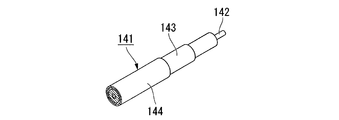
- FIGS. 11A to 13 for example, Patent Documents 1 and 2). reference.
- this method first, as shown in FIGS. 11A to 11B, the coaxial cable 141 is stripped to expose the inner conductor 142 and the outer conductor 143.
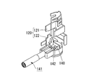
- FIG. 11D the inner conductor 142 of the coaxial cable 141 is soldered to the contact terminal 140 as shown in FIG. 11C.
- FIG. 12A the housing 122 is assembled into the shell terminal 121 to produce the assembly 120.
- FIG. 12A the housing 122 is assembled into the shell terminal 121 to produce the assembly 120.
- a coaxial cable 141 soldered to the contact terminal 140 is incorporated into the assembly 120.
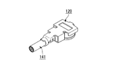
- the outer conductor 143 of the coaxial cable 141 and the shell terminal 121 are caulked, and the outer jacket 144 of the coaxial cable 141 and the shell terminal 121 are caulked.
- the assembly 120 connected to the coaxial cable 141 is attached to the RF module 130 as shown in FIG. 13, so that the coaxial cable 141 and the RF module 130 are electrically connected.
- the present invention has been made in view of the above circumstances, and an object of the present invention is to provide a cable connector and an antenna component that can reduce the number of assembling steps and the manufacturing cost and can reduce the thickness of the connector connecting portion.
- a cable connector of the present invention is a cable connector having a wiring board having a signal transmission path; and a plug connector provided on one surface of the wiring board and electrically connected to the signal transmission path.
- a first conductor, an insulating material, and a second conductor are sequentially laminated; a part of the second conductor is cut off by a slit formed in the second conductor.
- the signal transmission path is arranged at a predetermined distance from the second conductor; the second conductor and the signal transmission path are arranged on the same plane.
- the wiring board is formed by laminating the first conductor, the second conductor, and the third conductor via insulating materials.
- a coaxial cable electrically connected to the signal transmission path is disposed on one surface of the wiring board.
- the first notch is formed at a position facing the signal transmission path of the first conductor.
- the second notch is formed at a position facing the plug connector of the first conductor.
- An antenna component of the present invention includes a first wiring board having a signal transmission path; a plug connector provided on one surface of the first wiring board and electrically connected to the signal transmission path; An antenna component having an antenna electrically connected to a signal transmission path and having a second wiring board joined to the first wiring board, wherein the first wiring board includes a first conductor; An insulating material and a second conductor are sequentially laminated; and the signal transmission path in which a part of the second conductor is cut off from a slit formed in the second conductor is predetermined from the second conductor.
- the second conductor and the signal transmission line are arranged on the same plane.
- the first wiring board is formed by laminating the first conductor, the second conductor, and the third conductor via insulating materials.
- the first notch is formed at a position facing the signal transmission path of the first conductor.
- the second notch is formed at a position facing the plug connector of the first conductor.
- the second conductor and the signal transmission path are arranged on the same plane, and the second conductor is arranged on both sides of the signal transmission path.
- the thickness of the connecting portion between the connector and the mating connector can be reduced. Therefore, the thickness of the electronic device using this cable connector can be reduced.
- the plug connector can be easily mounted on the wiring board, the assembly process can be simplified. As a result, the manufacturing cost of the cable connector can be reduced. Furthermore, since the assembly process is simplified, it is difficult for variations in the performance of the cable connector to be manufactured, and a stable product can be provided.
- the characteristic impedance of the signal transmission path can be controlled easily. Therefore, it is possible to easily optimize the impedance of the wiring board according to the communication characteristics (frequency band, communication distance, etc.) at a high frequency of the device connected to the cable connector and the antenna.
- the thickness of the connection portion between the plug connector and the mating connector, the thickness of the joint portion between the first wiring board and the second wiring board, and the thickness of the antenna can be thin. Therefore, the thickness of the electronic device using this antenna component can be reduced.
- the plug connector can be easily mounted on the first wiring board, the assembly process can be simplified. As a result, the manufacturing cost of the antenna component can be reduced. Furthermore, since the assembly process is simplified, it is difficult for variations in the performance of the antenna components to be manufactured, and a stable product can be provided.
- the characteristic impedance of the signal transmission path can be changed. Can be controlled. Therefore, the impedance of the first wiring board can be easily optimized according to the high frequency communication characteristics (frequency band, communication distance, etc.) of the antenna of the second wiring board.
- FIG. 1A to 1E are schematic views showing a first embodiment of the cable connector of the present invention.
- FIG. 1A is a perspective view of the present embodiment.
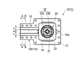
- FIG. 1B is a plan view of the present embodiment.
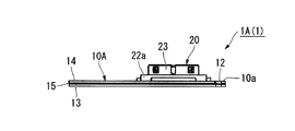
- FIG. 1C is a side view of the present embodiment.
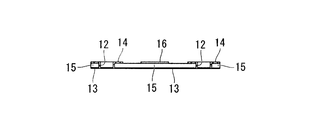
- FIG. 1D is a cross-sectional view taken along line AA in FIG. 1B.
- FIG. 1E is a cross-sectional view taken along line BB in FIG. 1B.
- the cable connector 1 ⁇ / b> A (1) of the present embodiment is schematically configured from a wiring board 10 ⁇ / b> A (10) and a plug connector 20.
- the wiring board 10A has a first conductor 13, an insulating material 15, and a second conductor 14, and these are laminated in order at substantially equal intervals.
- this insulating material 15 for example, polyimide resin, polyethylene terephthalate resin, aramid resin, liquid crystal polymer (LCP) or the like is used.
- a part of the second conductor 14 is cut to form a slit 11, and a signal transmission path 16 made of the same material as the second conductor 14 is provided in the slit 11 at a predetermined interval s from the second conductor 14. It is provided and arranged (see FIG. 2A).
- the second conductor 14 and the signal transmission path 16 are arranged on the same plane.
- the signal transmission path 16 is arranged so that both sides and the tip end side (plug connector 20 side) are surrounded by the second conductor 14.
- the plug connector 20 is provided on one surface 10 a of the wiring board 10 and is electrically connected to the signal transmission path 16.
- the first conductor 13 and the second conductor 14 form a ground wiring with respect to the signal transmission path 16. That is, in the wiring board 10 ⁇ / b> A, the signal transmission path 16 is disposed so as to overlap with a wide ground conductor (first conductor 13), and another ground conductor (second conductor 14) is connected to both sides and the tip of the signal transmission path 16.
- the signal transmission line 16 is disposed on the same plane so as to surround the side. With this structure, radiation noise emitted from the signal transmission path 16 is reduced.
- FIG. 2A is a plan view schematically showing the second conductor 14 and the signal transmission path 16.
- the second conductor 14 and the signal transmission path 16 are made of a metal foil such as copper, for example.
- the signal transmission path 16 is provided along the longitudinal direction of the second conductor 14 along the slit 11 provided in the central portion of the second conductor 14.
- the signal transmission path 16 is provided up to one end 14b of the second conductor 14 with the vicinity of the end of the region 14a facing the plug connector 20 in the second conductor 14 as the base end.
- the signal transmission path 16 is electrically connected to, for example, an antenna or the like at one end portion 14b of the second conductor 14 (not shown). Further, the signal transmission path 16 is arranged with a predetermined interval s from the second conductor 14.
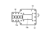
- FIG. 2B is a plan view schematically showing the first conductor 13. Similar to the second conductor 14 and the signal transmission path 16, the first conductor 13 is made of a metal foil such as copper. The first conductor 13 is formed with a plurality of rectangular first notches 13 a at positions facing the signal transmission path 16. Further, a second notch portion 13b larger than the first notch portion 13a is formed at a position of the first conductor 13 facing the plug connector 20. By forming the first notch portion 13a and the second notch portion 13b at this position, impedance matching of the wiring board 10A can be achieved, reflection loss of the electric signal can be reduced, and the transmission characteristics of the signal flowing through the signal transmission path 16 can be improved. Can be planned.
- first notches 13a and second notches 13b are not formed, when a thin substrate such as an FPC is used, the C component increases and its impedance decreases, and the signal is sufficiently transmitted. There is a risk of disappearing.
- the size of the first notch 13a is, for example, 0.5 mm ⁇ 0.5 mm.
- size of the 2nd notch part 13b is 2.1 mm x 1.05 mm, for example.
- a plurality of through holes 12 are provided at predetermined positions on the edges of the first conductor 13 and the second conductor 14 and the edges of the insulating material 15 disposed between them. ing. That is, these through holes 12 penetrate the wiring board 10 ⁇ / b> A (10) in the thickness direction and electrically connect the first conductor 13 and the second conductor 14.
- the distance d between the through holes 12 is a length corresponding to 1 ⁇ 2 wavelength or less of the frequency of the antenna connected to the cable connector 1A.
- the distance s between the second conductor 14 and the signal transmission path 16, the length and width w of the signal transmission path 16, the thickness of the first conductor 13, the second conductor 14, and the insulating material 15 are required for the wiring board 10A. It is adjusted appropriately according to the impedance to be adjusted. Thereby, the impedance of the wiring board 10A can be adjusted according to the communication characteristics (frequency band, communication distance, etc.) at a high frequency of the antenna connected to the cable connector 1A, and this impedance can be optimized.
- the impedance required for the wiring board 10A is 50 ⁇ . Therefore, for example, the interval s between the second conductor 14 and the signal transmission path 16 is 200 ⁇ m, the length of the signal transmission path 16 is 20 mm or less, the width w of the signal transmission path 16 is 450 ⁇ m, the thickness of the first conductor 13 is 18 ⁇ m, By setting the thickness of the second conductor 14 to 18 ⁇ m and the thickness of the insulating material 15 to 70 ⁇ m, a wiring board 10A having an impedance of 50 ⁇ can be obtained.
- the plug connector 20 includes a contact terminal 21, an insulator 22, and an external conductor 23.
- the contact terminal 21 comes into contact with a contact portion of a mating connector (receptacle connector) and is electrically connected to the receptacle connector. Further, the contact terminal 21 is electrically connected to the signal transmission path 16. That is, the signal transmission path 16 and the contact portion of the receptacle connector are electrically connected via the contact terminal 21.
- the insulator 22 includes a flat plate portion 22a and a raised portion 22b formed on one surface of the flat plate portion 22a. The raised portion 22b supports the contact terminal 21 so as to surround it.
- the plug connector 20 is disposed on the one surface 10 a of the wiring board 10 via the flat plate portion 22 a of the insulator 22.
- the insulator 22 is made of, for example, a liquid crystal polymer (LCP).
- the outer conductor 23 is disposed so as to surround the protruding portion 22 b of the insulator 22 from the outer periphery thereof, and is electrically connected to the first conductor 13 and the second conductor 14.
- the cable connector 1A of the present embodiment is used by connecting the plug connector 20 of the present embodiment to a receptacle connector 33 provided on one surface 31a of the insulating substrate 31, as shown in FIG. Specifically, the contact terminal 34 of the receptacle connector 33 is fitted to the contact terminal 21 of the plug connector 20, and the outer conductor 35 of the receptacle connector 33 is fitted to the outer conductor 23 of the plug connector 20. Electrically connected.
- the insulating substrate 31 is preferably provided with a through hole 32 as in the wiring substrate 10A of the present embodiment. At this time, the interval between the through holes 32 is a length corresponding to 1 ⁇ 2 wavelength or less of the frequency of the antenna connected to the cable connector 1A, similarly to the through hole 12 provided in the wiring board 10A.
- the cable connector 1A of the present embodiment since the wiring board 10A is used instead of the conventional coaxial cable, there is no need to consider the outer diameter of the coaxial cable, and the plug connector 20 and the receptacle connector 33 The thickness of the connecting portion can be reduced. Therefore, the thickness of the electronic device using the cable connector 1A of the present embodiment can be reduced.
- the impedance of the wiring board 10A can be adjusted according to the communication characteristics (frequency band, communication distance, etc.) at a high frequency of the antenna connected to the cable connector 1A, and this impedance can be optimized. Furthermore, if the plug connector 20 is mounted at a predetermined position on the wiring board 10A, the cable connector 1A of the present embodiment can be obtained.
- the assembly can be performed more easily than the conventional RF connector, and the assembly process can be simplified. That is, conventionally, referring to FIGS. 11A to 12D, strip processing of the coaxial cable 141, connection of the coaxial cable 141 and the contact terminal 140, production of the assembly 120, incorporation of the assembly 120 and the coaxial cable 141, and coaxial cable 141
- the outer conductor 143 and the shell terminal 121 are caulked, and the outer sheath 144 of the coaxial cable 141 and the shell terminal 121 are caulked.
- the first conductor 13, the insulating material 15, the second conductor 14, and the signal transmission path 16 are laminated (in a lump) to produce the wiring board 10A.
- the assembly of the cable connector 1A can be performed more easily than in the past. As a result, a special device or jig required for assembly is not required, the manufacturing cost of the cable connector 1A can be reduced, and the performance of the manufactured cable connector 1A is less likely to vary, and a stable product can be provided. .
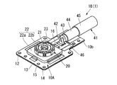
- FIG. 4 is a schematic perspective view showing a second embodiment of the cable connector of the present invention.
- the cable connector 1B (1) of the present embodiment is different from the cable connector 1A (1) of the first embodiment described above in that the plug connector 20 is provided on one surface of the first conductor 13 (the other surface 10b of the wiring board 10A).
- the point provided is that a coaxial cable 41 that is electrically connected to the signal transmission path 16 is disposed on one surface of the first conductor 13 at one end of the wiring board 10A.
- the coaxial cable 41 includes a central conductor 42 made of a single core wire or a stranded wire, an insulator 43 that covers the outer periphery thereof, an outer conductor 44 that is coaxially disposed outside the insulator 43, and an outer side of the outer conductor 44. And an outer cover 45 covering the surface.
- the coaxial cable 41 is disposed on one surface of the first conductor 13 constituting the wiring board 10A with the central conductor 42 exposed.
- the central conductor 42 is electrically connected to the signal transmission path 16 via, for example, a conductive member 46.
- the conductive member 46 is disposed in the first notch 13 a formed in the first conductor 13.
- the conductive member 46 is not particularly limited as long as the central conductor 42 and the signal transmission path 16 can be electrically connected, and may be a metal foil, solder, a conductive adhesive, or the like.
- the outer conductor 44 of the coaxial cable 41 is electrically connected to the first conductor 13.
- the coaxial cable 41 is connected to the wiring board 10 ⁇ / b> A, but the coaxial cable 41 is disposed away from the plug connector 20, and the coaxial cable 41 and the plug connector 20 are connected via the signal transmission path 16.
- the thickness of the connection portion between the cable connector 1B and the receptacle connector 33 of the present embodiment is the thickness of the wiring board 10A and the thickness of the plug connector 20 as in the first embodiment. Therefore, the thickness of the connecting portion can be made thinner than before.
- the coaxial cable 41 electrically connected to the signal transmission path 16 is disposed on the other surface 10b (one surface of the first conductor 13) of the wiring board 10A. Therefore, the signal transmission path (coaxial cable 41) can be routed more complicatedly over a longer distance in the casing of the electronic device than in the case of the first embodiment. Therefore, the deterioration of the communication characteristics at high frequencies can be suppressed by routing the signal transmission line (coaxial cable 41) having excellent high frequency characteristics.
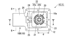
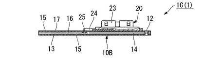
- FIG. 5A to 5D are schematic views showing a third embodiment of the cable connector of the present invention.
- FIG. 5A is a perspective view of the present embodiment.
- FIG. 5B is a plan view of the present embodiment.
- FIG. 5C is a cross-sectional view taken along line AA in FIG. 5B.
- FIG. 5D is a cross-sectional view taken along line BB in FIG. 5B.
- the cable connector 1C (1) of the present embodiment is different from the cable connector 1A (1) of the first embodiment described above in that the wiring board 10B (10) includes the first conductor 13, the second conductor 14, and the third conductor.
- the first conductor 13, the second conductor 14, and the third conductor 17 are sequentially stacked via the insulating material 15.
- the first conductor 13, the second conductor 14, and the third conductor 17 are electrically connected through a through hole 12 formed at the edge of the wiring board 10B.
- the distance d between the through holes 12 is a length corresponding to 1 ⁇ 2 wavelength or less of the frequency of the antenna connected to the cable connector 1C.
- the third conductor 17 is made of a metal foil such as copper.
- a first conductive portion 24 is provided on one surface of the third conductor 17 (one surface 10a of the wiring board 10B) via an insulating film 26 at a position corresponding to the signal transmission path 16.
- the plug connector 20 is disposed on the first conductive portion 24.
- the first conductive portion 24 is electrically connected to the contact terminal 21 of the plug connector 20 via a conductive portion (not shown) that penetrates the insulator 22 of the plug connector 20.
- the first conductive portion 24 is electrically connected to the signal transmission path 16 through the second conductive portion 25 penetrating the third conductor 17, the insulating film 26 and the insulating material 15.
- the outer conductor 23 is electrically connected to the third conductor 17.
- FIG. 6 is a plan view schematically showing the second conductor 14 and the signal transmission path 16 of the present embodiment.
- the signal transmission path 16 is provided along the longitudinal direction of the second conductor 14 along the slit 11 provided in the central portion of the second conductor 14 as in the first embodiment described above. It has been.
- the second conductor 14 is disposed at a predetermined interval s.
- a through hole 16a is provided near the tip of the signal transmission path 16 on the plug connector 20 side.
- the impedance required for the wiring board 10B is 50 ⁇ . Therefore, the distance s between the second conductor 14 and the signal transmission path 16 is 100 ⁇ m, the length of the signal transmission path 16 is 50 mm or less, the width w of the signal transmission path 16 is 85 ⁇ m, the thickness of the first conductor 13 is 18 ⁇ m, The thickness of the second conductor 14 is 18 ⁇ m, the thickness of the third conductor 17 is 18 ⁇ m, the thickness of the insulating material 15 disposed between the second conductor 14 and the third conductor 17 is 70 ⁇ m, and the first conductor 13 and the first conductor 13 The thickness of the insulating material 15 disposed between the two conductors 14 is 67 ⁇ m.
- a first notch is provided at a position facing the signal transmission path 16 of the first conductor 13 and faces the plug connector 20 of the first conductor 13. It is preferable that a second notch is provided at the position (not shown in the figure). Further, in the third conductor 17 as well, a first notch is provided at a position facing the signal transmission path 16 of the third conductor 17 and at a position facing the plug connector 20 of the third conductor 17. The second cutout is preferably provided (not shown in the figure).
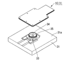
- FIG. 7 is a perspective view showing an example of how to use the cable connector 1C of the present embodiment.
- the plug connector 20 of the present embodiment is connected to the receptacle connector 33 provided on the one surface 31a of the insulating substrate 31, similarly to the first embodiment.
- the contact terminal 34 of the receptacle connector 33 is fitted to the contact terminal 21 of the plug connector 20, and the outer conductor 35 of the receptacle connector 33 is fitted to the outer conductor 23 of the plug connector 20. Electrically connected.
- the insulating substrate 31 having a configuration in which no through hole is provided is shown.
- the insulating substrate 31 may be provided with a through hole. At this time, the distance between the through holes is a length corresponding to 1 ⁇ 2 wavelength or less of the frequency of the antenna connected to the cable connector 1C.
- the same effect as that obtained in the first embodiment described above can be obtained.
- the wiring board 10 since the wiring board 10 is composed of the first conductor 13, the second conductor 14, the third conductor 17, and the insulating material 15 disposed therebetween, the wiring board 10 of the first embodiment
- the thickness of the connecting portion between the plug connector 20 and the receptacle connector 33 increases by the thickness of the third conductor 13 and the one-layer insulating material 15.
- the thickness of the connecting portion is still sufficiently thin. Further, as shown in FIG.
- the signal transmission path 16 is surrounded by the ground conductors (the first conductor 13, the second conductor 14, and the third conductor 17), so that it is more than the cable connector 1 ⁇ / b> A of the first embodiment. Radiation noise can be reduced and signal transmission characteristics are improved. Therefore, the wiring board 10B can be routed longer than in the first embodiment. Therefore, the cable connectors 1A and 1C according to the first embodiment or the third embodiment may be applied according to the size of the electronic device to be applied, the length of routing, and the required radiation noise characteristics.
- FIG. 8 is a perspective view showing a fourth embodiment of the cable connector of the present invention.
- the cable connector 1D (1) of the present embodiment is different from the cable connector 1C (1) of the third embodiment described above in that a signal transmission line is provided on one surface of the third conductor 17 at one end of the wiring board 10B.
- 16 is provided with a coaxial cable 41 electrically connected to 16.
- the coaxial cable 41 the thing similar to what was used in 2nd embodiment is applicable.
- the central conductor 42 of the coaxial cable 41 is electrically connected to the signal transmission path 16 via the conductive member 46, and the outer conductor 44 of the coaxial cable 41 is electrically connected to the third conductor 17.
- the conductive member 46 is disposed in a through hole that penetrates the third conductor 17 and the insulating material 15 disposed between the third conductor 17 and the second conductor 14. Yes.
- the conductive member 46 is the same as in the second embodiment.
- the wiring board 10B is composed of the first conductor 13, the second conductor 14, the third conductor 17, and the insulating material 15 disposed between them, and therefore the first embodiment.
- the thickness of the connecting portion between the plug connector 20 and the receptacle connector 33 is increased by the third conductor 13 and the one-layer insulating material 15.
- the thickness of the connecting portion is still sufficiently thin.
- the signal transmission path 16 is surrounded by the ground conductors (the first conductor 13, the second conductor 14, and the third conductor 17), radiation noise can be reduced as compared with the cable connector 1B of the second embodiment.
- the transmission characteristics are improved. Therefore, the signal transmission path (coaxial cable 41) can be routed longer than in the second embodiment. Therefore, the cable connectors 1B and 1D according to the second embodiment or the fourth embodiment may be applied according to the size of the electronic device to be applied, the length of routing, and the required radiation noise characteristics.
- FIG. 9 is a schematic perspective view showing a first embodiment of the antenna component of the present invention and a method for using the antenna component.
- the antenna component 50A (50) of the present embodiment is schematically configured from the cable connector 1A (wiring board 10A and plug connector 20) of the first embodiment and the second wiring board 60A (60).
- the wiring board 10A of the cable connector 1A may be referred to as a first wiring board 10A.
- the second wiring board 60 is bonded to the first wiring board 10A.
- the second wiring board 60A is provided with an antenna 65A (65) that is electrically connected to the signal transmission path 16 of the first wiring board 10A.
- the plurality of through holes 12 provided at the edge of the first wiring board 10A have a distance d corresponding to a half wavelength or less of the frequency of the antenna 65A.
- the second wiring board 60 ⁇ / b> A is schematically configured by a flexible board 62; and an antenna 65 ⁇ / b> A composed of a conductor 63 and a ground conductor 64 provided on one surface 62 a of the board 62.
- the conductor 63 is electrically connected to the signal transmission path 16 of the first wiring board 10A.
- the conductor 63 may be integrated with the signal transmission path 16.
- the ground conductor 64 is electrically connected to the first conductor 13 of the first wiring board 10A.
- the ground conductor 64 may be integrated with the first conductor 13 as shown in FIG.
- a film-like or sheet-like resin made of polyimide resin, polyethylene terephthalate resin, aramid resin or the like is used.
- the conductor 63 and the ground conductor 64 one surface 62a of the substrate 62 formed by screen printing in a predetermined pattern using a conductive paste, one obtained by etching a conductive foil, Or what is formed by metal plating is mentioned.
- the conductive paste forming the conductor 63 and the ground conductor 64 include conductive materials such as silver powder, gold powder, platinum powder, aluminum powder, palladium powder, rhodium powder, and carbon powder (carbon black, carbon nanotube, etc.). The thing by which microparticles
- the conductive foil constituting the conductor 63 and the ground conductor 64 include copper foil, silver foil, gold foil, platinum foil, and aluminum foil.
- the metal plating forming the conductor 63 and the ground conductor 64 include copper plating, silver plating, gold plating, and platinum plating.
- the antenna component 50A of the present embodiment is also used by being connected to the receptacle connector 33 in the same manner as the cable connector 1A.
- the through holes 32 are also provided in the substrate 31 on which the receptacle connector 33 is provided at intervals corresponding to 1 ⁇ 2 wavelength or less of the frequency of the antenna 65A.
- the first wiring board 10A is provided instead of the conventional coaxial cable. As in the case, the thickness of the connecting portion between the plug connector 20 and the receptacle connector 33 can be reduced. Further, since the second wiring board 60A provided with the antenna 65A is joined to the first wiring board 10A, and the antenna 65A and the signal transmission path 17 are electrically connected, the first wiring board 10A and the second wiring board are connected. The thickness of the joint with 60A is about the thickness of the first wiring board 10A and the thickness of the second wiring board 60A.
- the thickness of the joint portion between the antenna 65A and the first wiring board 10A can be made much thinner than the thickness of the joint portion between the coaxial cable and the antenna when a conventional coaxial cable is used.
- the thickness of the antenna 65A (second wiring board 60A) itself is about the thickness of the board 62 and is thin
- the antenna component 50A of the present embodiment is mounted on the electronic equipment, so that the electronic equipment The thickness can be reduced.
- the antenna connector 50A of the present embodiment uses the cable connector 1A described above, the antenna component 50A described above is described above according to the communication characteristics (frequency band, communication distance, etc.) at the high frequency of the antenna 65A of the second wiring board 60A.
- the impedance of the first wiring board 10A can be adjusted and the impedance can be optimized. Therefore, power can be transmitted efficiently and a sufficient communication distance can be secured. Furthermore, since the plug connector 20 can be easily mounted on the first wiring board 10A, that is, the antenna component 50A of the present embodiment is manufactured simply by mounting the plug connector 20 on the FPC on which the antenna 65A is formed. Therefore, the assembly process can be simplified similarly to the above-described cable connector 1A. As a result, special devices and jigs required for assembly are not required, so that the manufacturing cost can be reduced, and the performance of the manufactured antenna component 50A is less likely to vary, and a stable product can be provided.
- FIG. 10 is a schematic perspective view showing a second embodiment of the antenna component of the present invention and a method for using the antenna component.
- the antenna component 50B (50) of the present embodiment is different from the antenna component 50A of the first embodiment described above in that the cable connector 1C (the wiring board 10B and the plug connector 20) according to the third embodiment is second.
- the wiring board 60 ⁇ / b> B (60) is joined, and the antenna 65 ⁇ / b> B (65) is composed of the first conductor 66, the second conductor 67, and the third conductor 68.
- the wiring board 10B of the cable connector 1C may be referred to as a first wiring board 10B.
- the second wiring board 60B (60) of the present embodiment includes a flexible substrate 62; a first conductor 66, a second conductor 67, and a third conductor provided on one surface 62a of the substrate 62.
- the second conductor 67 and the third conductor 68 are electrically connected to the signal transmission path 16 of the first wiring board 10B.
- the lengths of the first conductor 66, the second conductor 67, and the third conductor 68 constituting the antenna correspond to a quarter wavelength of the frequency of the electronic device to which the antenna component 50B of the present embodiment is applied. It is the length to do.
- the first conductor 66, the second conductor 67, and the third conductor 68 are formed on one surface of the substrate 62 in the same manner as the conductor 63 and the ground conductor 64 applied to the antenna component 50A of the first embodiment. 62a can be formed.
- the antenna component 50B of the present embodiment is also used by being connected to the receptacle connector 33 in the same manner as the cable connector 1C described above. At this time, although not shown in FIG. 10, even though the substrate 31 provided with the receptacle connector 33 is provided with through holes at intervals corresponding to 1 ⁇ 2 wavelength or less of the frequency of the antenna 65B. Good.
- the first wiring board 10B is composed of the first conductor 13, the second conductor 14, the third conductor 17, and the insulating material 15 disposed therebetween, so the first embodiment
- the thickness of the connecting portion between the plug connector 20 and the receptacle connector 33 and the thickness of the connecting portion between the first wiring board 10B and the second wiring board 60B are more than the third conductor 13 and the one-layer insulating material. It will increase by the thickness of 15. However, compared with the case where the conventional coaxial cable is used, the thickness of the connecting portion is still sufficiently thin.
- the signal transmission path 16 is surrounded by the ground conductors (the first conductor 13, the second conductor 14, and the third conductor 17), radiation noise can be reduced compared to the antenna component 50B of the first embodiment, and the signal The transmission characteristics are improved. Therefore, the signal transmission path (first wiring board 10B) can be routed longer than in the first embodiment. Therefore, the antenna components 50A and 50B according to the first embodiment or the second embodiment may be applied according to the size of the electronic device to be applied, the length of routing, and the required radiation noise characteristics.
- the thickness of the connecting portion between the plug connector and the mating connector can be reduced.
- the plug connector can be easily mounted on the wiring board, the assembly process can be simplified. As a result, the manufacturing cost of the cable connector can be reduced. Further, since the assembly process is simplified, it is difficult for variations in the performance of the cable connector to be manufactured, and a stable product can be provided. Furthermore, it is possible to easily optimize the impedance of the wiring board according to the communication characteristics (frequency band, communication distance, etc.) of the device connected to the cable connector and the antenna at high frequencies.
- the thickness of the connection portion between the plug connector and the receptacle connector, and the thickness of the joint portion between the first wiring board and the second wiring board are compared with the case where a conventional coaxial cable is used. Can also be thinned.
- the antenna component of this embodiment is produced only by mounting the plug connector on the FPC on which the antenna is formed, the assembly process can be simplified. As a result, the manufacturing cost can be reduced, and variations in the performance of the manufactured antenna parts are less likely to occur, and a stable product can be provided.
- the impedance of the first wiring board can be lowered and the impedance can be optimized according to the communication characteristics (frequency band, communication distance, etc.) at high frequencies of the antenna. Therefore, according to the antenna component of the present invention, power can be transmitted efficiently and a sufficient communication distance can be secured.
- Cable connector 10 (10A, 10B) Wiring board (first wiring board) 11 Slit 12 Through Hole 13 First Conductor 14 Second Conductor 15 Insulating Material 16 Signal Transmission Line 17 Third Conductor 20 Plug Connector 21 Contact Terminal 22 Insulator 22a Flat Plate Part 22b Raised Part 23 External Conductor 31 Insulating Substrate 32 Through Hole 33 Receptacle connector 34 Contact terminal 35 Outer conductor 41 Coaxial cable 42 Center conductor 43 Insulator 44 Outer conductor 45 Outer sheath 46 Conductive member 50 (50A, 50B) Antenna component 60 (60A, 60B) Second wiring board 62 Substrate 63 Conductor 64 Ground conductor 65 (65A, 65B) Antenna 66 First conductor 67 Second conductor 68 Third conductor
Landscapes
- Coupling Device And Connection With Printed Circuit (AREA)
Abstract
Description
本願は、2008年12月16日に、日本国に出願された特願2008-319520号と、2008年12月16日に、日本国に出願された特願2008-319946号とに基づき優先権を主張し、その内容をここに援用する。
また、同軸ケーブルの外径が大きいため、同軸ケーブルとRF用コネクタとの接続部(コネクタ接続部)の厚さ(すなわち、図12Dに示すアッセンブリー120の厚さ)を薄く(低背化)することが困難である。
さらに、RF用コネクタと同軸ケーブルとの組立工程が多いため、これらの製造コストが高くなる。
(1)本発明のケーブルコネクタは、信号伝送路を有する配線基板と;前記配線基板の一方の面に設けられ、前記信号伝送路と電気的に接続されたプラグコネクタと;を有するケーブルコネクタであって:前記配線基板は、第一導体と、絶縁材と、第二導体とが順に積層されてなり;前記第二導体に形成されたスリットに、前記第二導体の一部が切り離されてなる前記信号伝送路が、前記第二導体から所定の間隔を設けて配置され;前記第二導体と前記信号伝送路とが同一平面上に配置されている。
(2)上記(1)の場合、前記配線基板が、前記第一導体と、前記第二導体と、第三導体とが、それぞれ絶縁材を介して積層されてなるのが好ましい。
(3)上記(1)または(2)の場合、前記配線基板の一方の面に、前記信号伝送路と電気的に接続される同軸ケーブルが配設されているのが好ましい。
(4)上記(1)または(2)の場合、第一切欠部が、前記第一導体の前記信号伝送路と対向する位置に形成されているのが好ましい。
(5)上記(4)の場合、第二切欠部が、前記第一導体の前記プラグコネクタと対向する位置に形成されているのが好ましい。
(7)上記(6)の場合、前記第一配線基板が、前記第一導体と、前記第二導体と、第三導体とが、それぞれ絶縁材を介して積層されてなるのが好ましい。
(8)上記(6)または(7)の場合、第一切欠部が、前記第一導体の前記信号伝送路と対向する位置に形成されているのが好ましい。
(9)上記(8)の場合、第二切欠部が、前記第一導体の前記プラグコネクタと対向する位置に形成されているのが好ましい。
また、配線基板に対してプラグコネクタを容易に実装できるので、組立工程の簡略化が行なえる。その結果、ケーブルコネクタの製造コストの削減ができる。さらに、組立工程が簡略化されることから、製造されるケーブルコネクタの性能にばらつきが生じ難くなり、安定した製品の提供が可能となる。
さらに、信号伝送路の幅や長さ、信号伝送路と第二導体との間の間隙の大きさ、第一導体、および第二導体の厚さ等を変えることで、信号伝送路の特性インピーダンスを容易に制御できる。したがって、ケーブルコネクタに接続される機器やアンテナの高周波における通信特性(周波数帯、通信距離など)に応じて、配線基板のインピーダンスを容易に最適化できる。
また、第一配線基板に対してプラグコネクタを容易に実装できるので、組立工程の簡略化が行なえる。その結果、アンテナ部品の製造コストを削減できる。さらに、組立工程が簡略化されることから、製造されるアンテナ部品の性能にばらつきが生じ難くなり、安定した製品の提供が可能となる。
さらに、信号伝送路の幅や長さ、信号伝送路と第二導体との間の間隙の大きさ、第一導体、および第二導体の厚さを変えることで、信号伝送路の特性インピーダンスを制御できる。したがって、第二配線基板のアンテナの高周波における通信特性(周波数帯、通信距離など)に応じて、第一の配線基板のインピーダンスを容易に最適化できる。
なお、この形態は、発明の趣旨をより良く理解させるために具体的に説明するものであり、特に指定のない限り、本発明を限定するものではない。
図1A~Eは、本発明のケーブルコネクタの第一実施形態を示す概略図である。図1Aは、本実施形態の斜視図である。図1Bは、本実施形態の平面図である。図1Cは、本実施形態の側面図である。図1Dは、図1BのA-A線に沿う断面図である。図1Eは、図1BのB-B線に沿う断面図である。
本実施形態のケーブルコネクタ1A(1)は、配線基板10A(10)と、プラグコネクタ20とから概略構成されている。
配線基板10Aは、第一導体13と、絶縁材15と、第二導体14と、を有し、これらがほぼ等間隔に順に積層されてなる。この絶縁材15としては、例えばポリイミド樹脂、ポリエチレンテレフタレート樹脂、アラミド樹脂、液晶ポリマー(LCP)などが用いられる。
第二導体14には、その一部が切り離されてスリット11が形成され、このスリット11に第二導体14と同一の材質からなる信号伝送路16が、第二導体14から所定の間隔sを設けて配置されている(図2A参照)。この第二導体14と信号伝送路16とが、同一平面上に配されている。すなわち、信号伝送路16は、その両側と先端側(プラグコネクタ20側)が、第二導体14で囲まれるように配されている。
プラグコネクタ20は、配線基板10の一方の面10aに設けられ、信号伝送路16と電気的に接続されている。
第二導体14と信号伝送路16とは、例えば銅などの金属箔から構成されている。
信号伝送路16は、図2Aに示すように、第二導体14の中央部に設けられたスリット11に沿って、第二導体14の長手方向に沿って設けられている。この信号伝送路16は、第二導体14におけるプラグコネクタ20に対向する領域14aの端部近傍を基端とし、第二導体14の一端14bまで設けられている。この信号伝送路16は、第二導体14の一端部14bにて、例えばアンテナ等と電気的に接続されている(図示略)。
また、信号伝送路16は、第二導体14から所定の間隔sを設けて配置されている。
第一導体13は、第二導体14や信号伝送路16と同様に、例えば銅などの金属箔から構成されている。
この第一導体13には、信号伝送路16と対向する位置に、矩形状の第一切欠部13aが複数形成されている。また、第一導体13の、プラグコネクタ20に対向する位置には、第一切欠部13aよりも大きな第二切欠部13bが形成されている。第一切欠部13aおよび第二切欠部13bをこの位置に形成することで配線基板10Aのインピーダンス整合が図れ、電気信号の反射損失が低減され、信号伝送路16を流れる信号の伝送特性の向上が図れる。これらの第一切欠部13aおよび第二切欠部13bが形成されていないと、FPCのような薄型基板を用いた場合、C成分が増加してそのインピーダンスが低下し、信号が十分に伝送されなくなる虞がある。
第一切欠部13aの大きさは、例えば、0.5mm×0.5mmである。
第二切欠部13bの大きさは、例えば、2.1mm×1.05mmである。
これらのスルーホール12同士の間隔dは、ケーブルコネクタ1Aに接続されるアンテナの周波数の1/2波長以下に相当する長さである。
接触端子21は、相手コネクタ(リセプタクルコネクタ)の接触部と接触し、このリセプタクルコネクタと電気的に接続される。また、この接触端子21は、信号伝送路16と電気的に接続されている。すなわち、接触端子21を介して、信号伝送路16とリセプタクルコネクタの接触部とが電気的に接続される。
絶縁体22は、平板部22aと、この平板部22aの一面に形成された隆起部22bとからなる。この隆起部22bが、接触端子21を包囲するようにして支持する。プラグコネクタ20は、絶縁体22の平板部22aを介して配線基板10の一面10aに配置されている。この絶縁体22は、例えば液晶ポリマー(LCP)からなる。
外部導体23は、絶縁体22の隆起部22bをその外周から囲むように配置され、第一導体13および第二導体14と電気的に接続されている。
また、ケーブルコネクタ1Aに接続されるアンテナの高周波における通信特性(周波数帯、通信距離など)に応じて、配線基板10Aのインピーダンスを調整できるとともに、このインピーダンスを最適化できる。
さらに、配線基板10Aの所定の位置にプラグコネクタ20を実装すれば、本実施形態のケーブルコネクタ1Aが得られるので、従来のRF用コネクタよりも容易に組立が行なえ、組立工程を簡略化できる。すなわち、従来では、図11Aから図12Dを参照すると、同軸ケーブル141のストリップ加工、同軸ケーブル141とコンタクト端子140との接続、アッセンブリー120の作製、アッセンブリー120と同軸ケーブル141との組み込み、同軸ケーブル141の外部導体143とシェル端子121とのかしめ、および同軸ケーブル141の外被144とシェル端子121とのかしめ、の工程が必要だった。これに対し、本実施形態によれば、第一導体13と、絶縁材15と、第二導体14および信号伝送路16とを(一括で)積層して配線基板10Aを作製し、さらにこの配線基板10の所定の位置にプラグコネクタ20を実装すればよいので、従来よりもケーブルコネクタ1Aの組立が容易に行なえる。その結果、組立に要する特殊な装置や冶具が不要となり、ケーブルコネクタ1Aの製造コストを削減でき、かつ製造されるケーブルコネクタ1Aの性能にばらつきが生じ難くなり、安定した製品の提供が可能となる。
図4は、本発明のケーブルコネクタの第二実施形態を示す概略斜視図である。
図4において、図1A~2Bに示した第一実施形態の構成要素と同じ構成要素には同一符号を付して、その説明を省略する。
本実施形態のケーブルコネクタ1B(1)が、上述の第一実施形態のケーブルコネクタ1A(1)と異なる点は、第一導体13の一面(配線基板10Aの他面10b)にプラグコネクタ20が設けられている点と、配線基板10Aの一端部において、第一導体13の一面に信号伝送路16と電気的に接続される同軸ケーブル41が配設されている点である。
この同軸ケーブル41は、配線基板10Aをなす第一導体13の一面に、その中心導体42が露出して配置されている。この中心導体42が、例えば導電部材46を介して信号伝送路16と電気的に接続されている。この導電部材46は、第一導体13に形成された第一切欠部13a内に配置している。この導電部材46は、中心導体42と信号伝送路16とを電気的に接続できれば特に限定されるものではなく、金属箔やはんだ、導電性接着材等であってもよい。
また、同軸ケーブル41の外部導体44が、第一導体13と電気的に接続されている。
さらに、本実施形態のケーブルコネクタ1Bでは、配線基板10Aの他方の面10b(第一導体13の一面)に、信号伝送路16と電気的に接続された同軸ケーブル41が配設されている。そのため、電子機器の筐体内において、第一実施形態の場合よりも信号伝送路(同軸ケーブル41)を長距離に渡って複雑に引き回すことができる。したがって、高周波特性に優れた信号伝送路(同軸ケーブル41)を引き回すことで、高周波における通信特性の劣化を抑制できる。
図5A~5Dは、本発明のケーブルコネクタの第三実施形態を示す概略図である。図5Aは、本実施形態の斜視図である。図5Bは、本実施形態の平面図である。図5Cは、図5BのA-A線に沿う断面図である。図5Dは、図5BのB-B線に沿う断面図である。
図5A~5Dにおいて、上述の第一実施形態の構成要素と同じ構成要素には同一符号を付して、その説明を省略する。
本実施形態のケーブルコネクタ1C(1)が上述の第一実施形態のケーブルコネクタ1A(1)と異なる点は、配線基板10B(10)が、第一導体13と第二導体14と第三導体17とが、それぞれ絶縁材15を介して順に積層されている点である。これら第一導体13と第二導体14と第三導体17とが、配線基板10Bの縁部に形成されたスルーホール12を介して電気的に接続されている。スルーホール12同士の間隔dは、本実施形態においても、ケーブルコネクタ1Cに接続されるアンテナの周波数の1/2波長以下に相当する長さである。
この第三導体17の一面(配線基板10Bの一面10a)には、信号伝送路16に対応する位置に、絶縁膜26を介して第一導電部24が設けられている。そして、この第一導電部24上に、プラグコネクタ20が配されている。この第一導電部24が、プラグコネクタ20の絶縁体22を貫通する導電部(図示略)を介して、プラグコネクタ20の接触端子21と電気的に接続されている。
さらに、第一導電部24は、第三導体17、絶縁膜26および絶縁材15を貫通する第二導電部25を介して、信号伝送路16と電気的に接続されている。
また、外部導体23は、第三導体17と電気的に接続されている。
この信号伝送路16のプラグコネクタ20側の先端部近傍には、スルーホール16aが設けられている。このスルーホール16aに第二導電部25が配置されることで、信号伝送路16と第一導電部24とが電気的に接続される。
図7では、絶縁性基板31としてスルーホールが設けられていない構成のものを示しているが、第一実施形態の際と同様に、この絶縁性基板31にスルーホールを設けてもよい。この際、スルーホール同士の間隔は、ケーブルコネクタ1Cに接続されるアンテナの周波数の1/2波長以下に相当する長さとなる。
さらに、図5Dに示すように、信号伝送路16がグラウンド導体(第一導体13、第二導体14、および第三導体17)で囲まれているため、第一実施形態のケーブルコネクタ1Aよりも放射ノイズが軽減でき、信号の伝送特性が向上する。したがって、第一実施形態よりも、より長く配線基板10Bの引き回しが可能となる。ゆえに、適用する電子機器の大きさや、引き回しの長さ、および求められる放射ノイズ特性に応じて、第一実施形態あるいは第三実施形態に係るケーブルコネクタ1A,1Cを適用すればよい。
図8は、本発明のケーブルコネクタの第四実施形態を示す斜視図である。
本実施形態のケーブルコネクタ1D(1)が、上述の第三の実施形態のケーブルコネクタ1C(1)と異なる点は、配線基板10Bの一端部において、第三導体17の一面に、信号伝送路16と電気的に接続される同軸ケーブル41が配設されている点である。
この同軸ケーブル41としては、第二実施形態で用いたものと同様なものを適用できる。本実施形態においても、同軸ケーブル41の中心導体42が、導電部材46を介して信号伝送路16と電気的に接続され、同軸ケーブル41の外部導体44が第三導体17と電気的に接続されている。本実施形態にあっては、第三導体17と、この第三導体17および第二導体14の間に配された絶縁材15と、を貫通する貫通孔内に、導電部材46が配されている。この導電部材46としては、第二実施形態と同様である。
さらに、信号伝送路16がグラウンド導体(第一導体13、第二導体14、および第三導体17)で囲まれているため、第二実施形態のケーブルコネクタ1Bよりも放射ノイズが軽減でき、信号の伝送特性が向上する。したがって、第二実施形態よりも、より長く信号伝送路(同軸ケーブル41)の引き回しが可能となる。ゆえに、適用する電子機器の大きさや、引き回しの長さ、および求められる放射ノイズ特性に応じて、第二実施形態あるいは第四実施形態に係るケーブルコネクタ1B,1Dを適用すればよい。
次に、本発明のアンテナ部品の形態について説明する。
なお、この形態は、発明の趣旨をより良く理解させるために具体的に説明するものであり、特に指定のない限り、本発明を限定するものではない。
図9は、本発明のアンテナ部品の第一実施形態およびその使用方法を示す概略斜視図である。
本実施形態のアンテナ部品50A(50)は、上述の第一実施形態のケーブルコネクタ1A(配線基板10Aおよびプラグコネクタ20)と、第二配線基板60A(60)とから概略構成されている。以下、ケーブルコネクタ1Aの配線基板10Aを、第一配線基板10Aということがある。
第二配線基板60は、第一配線基板10Aに接合される。この第二配線基板60Aには、第一配線基板10Aの信号伝送路16と電気的に接続されるアンテナ65A(65)が設けられている。
導電体63は、第一配線基板10Aの信号伝送路16に電気的に接続されている。この導電体63は、信号伝送路16と一体をなしていてもよい。
グランド導電体64は、第一配線基板10Aの第一導体13と電気的に接続されている。このグランド導電体64は、図9に示すように第一導体13と一体をなしていてもよい。
導電体63、およびグランド導電体64をなす導電性ペーストとしては、例えば、銀粉末、金粉末、白金粉末、アルミニウム粉末、パラジウム粉末、ロジウム粉末、カーボン粉末(カーボンブラック、カーボンナノチューブなど)などの導電微粒子が樹脂組成物に配合されたものが挙げられる。
導電体63、およびグランド導電体64をなす導電性箔としては、銅箔、銀箔、金箔、白金箔、アルミニウム箔などが挙げられる。
導電体63、およびグランド導電体64をなす金属メッキとしては、銅メッキ、銀メッキ、金メッキ、白金メッキなどが挙げられる。
また、本実施形態のアンテナ部品50Aでは、上述のケーブルコネクタ1Aを用いていることから、第二配線基板60Aのアンテナ65Aの高周波における通信特性(周波数帯、通信距離など)に応じて、上述したように、この第一配線基板10Aのインピーダンスを調整できるとともに、インピーダンスを最適化できる。したがって、効率よく電力を伝達することができ、十分な通信距離を確保できる。
さらに、第一配線基板10Aに対してプラグコネクタ20を容易に実装できるので、すなわち、アンテナ65Aが形成されたFPCにプラグコネクタ20を実装するだけで、本実施形態のアンテナ部品50Aが作製されるので、上述のケーブルコネクタ1Aと同様に、その組立工程を簡略化できる。その結果、組立に要する特殊な装置や冶具が不要となるため、製造コストを削減でき、かつ製造されるアンテナ部品50Aの性能にばらつきが生じ難くなり、安定した製品の提供が可能となる。
図10は、本発明のアンテナ部品の第二実施形態およびその使用方法を示す概略斜視図である。
本実施形態のアンテナ部品50B(50)が、上述の第一実施形態のアンテナ部品50Aと異なる点は、上述の第三実施形態に係るケーブルコネクタ1C(配線基板10Bおよびプラグコネクタ20)に第二配線基板60B(60)が接合されている点、およびアンテナ65B(65)が第一導電体66、第二導電体67、および第三導電体68からなる点である。以下、ケーブルコネクタ1Cの配線基板10Bを、第一配線基板10Bということがある。
これらの導電体のうち、第一導電体66が第一配線基板10Bの第一導体13と電気的に接続され、グラウンド導体となっている。一方、第二導電体67、および第三導電体68が、第一配線基板10Bの信号伝送路16と電気的に接続されている。アンテナを構成するこれら第一導電体66、第二導電体67、および第三導電体68の長さは、本実施形態のアンテナ部品50Bが適用される電子機器の周波数の1/4波長に相当する長さとなっている。これら第一導電体66、第二導電体67、および第三導電体68は、第一実施形態のアンテナ部品50Aに適用されている導電体63およびグランド導電体64と同様にして基板62の一面62aに形成できる。
さらに、信号伝送路16がグラウンド導体(第一導体13、第二導体14、および第三導体17)で囲まれているため、第一実施形態のアンテナ部品50Bよりも放射ノイズが軽減でき、信号の伝送特性が向上する。したがって、第一実施形態よりも、より長く信号伝送路(第一配線基板10B)の引き回しが可能となる。
したがって、適用する電子機器の大きさや、引き回しの長さ、および求められる放射ノイズ特性に応じて、第一実施形態あるいは第二実施形態に係るアンテナ部品50A,50Bを適用すればよい。
本発明のアンテナ部品によれば、プラグコネクタとリセプタクルコネクタとの接続部の厚さ、および第一配線基板と第二配線基板との接合部の厚さを、従来の同軸ケーブルを用いた場合よりも薄くできる。また、アンテナが形成されたFPCにプラグコネクタを実装するだけで、本実施形態のアンテナ部品が作製されるので、その組立工程を簡略化できる。その結果、製造コストを削減でき、かつ製造されるアンテナ部品の性能にばらつきが生じ難くなり、安定した製品の提供が可能となる。さらに、アンテナの高周波における通信特性(周波数帯、通信距離など)に応じて、第一配線基板のインピーダンスを低くできるとともに、インピーダンスを最適化できる。したがって、本発明のアンテナ部品によれば、効率よく電力を伝達することができ、十分な通信距離を確保できる。
10(10A,10B) 配線基板(第一配線基板)
11 スリット
12 スルーホール
13 第一導体
14 第二導体
15 絶縁材
16 信号伝送路
17 第三導体
20 プラグコネクタ
21 接触端子
22 絶縁体
22a 平板部
22b 隆起部
23 外部導体
31 絶縁性基板
32 スルーホール
33 リセプタクルコネクタ
34 接触端子
35 外部導体
41 同軸ケーブル
42 中心導体
43 絶縁体
44 外部導体
45 外被
46 導電部材
50(50A,50B) アンテナ部品
60(60A,60B) 第二配線基板
62 基板
63 導電体
64 グランド導電体
65(65A,65B) アンテナ
66 第一導電体
67 第二導電体
68 第三導電体
Claims (9)
- 信号伝送路を有する配線基板と;
前記配線基板の一方の面に設けられ、前記信号伝送路と電気的に接続されたプラグコネクタと;
を有するケーブルコネクタであって:
前記配線基板は、第一導体と、絶縁材と、第二導体とが順に積層されてなり;
前記第二導体に形成されたスリットに、前記第二導体の一部が切り離されてなる前記信号伝送路が、前記第二導体から所定の間隔をあけて配置され;
前記第二導体と前記信号伝送路とが同一平面上に配置されている;
ことを特徴とするケーブルコネクタ。 - 前記配線基板が、前記第一導体と、前記第二導体と、第三導体とが、それぞれ絶縁材を介して順に積層されてなることを特徴とする請求項1に記載のケーブルコネクタ。
- 前記配線基板の一方の面に、前記信号伝送路と電気的に接続される同軸ケーブルが配設されていることを特徴とする請求項1または2に記載のケーブルコネクタ。
- 第一切欠部が、前記第一導体の前記信号伝送路と対向する位置に形成されていることを特徴とする請求項1または2に記載のケーブルコネクタ。
- 第二切欠部が、前記第一導体の前記プラグコネクタと対向する位置に形成されていることを特徴とする請求項4に記載のケーブルコネクタ。
- 信号伝送路を有する第一配線基板と;
前記第一配線基板の一方の面に設けられ、前記信号伝送路と電気的に接続されたプラグコネクタと;
前記信号伝送路と電気的に接続されたアンテナを有し、前記第一配線基板に接合された第二配線基板と、を有するアンテナ部品であって:
前記第一配線基板は、第一導体と、絶縁材と、第二導体とが順に積層されてなり;
前記第二導体に形成されたスリットに、前記第二導体の一部が切り離されてなる前記信号伝送路が、前記第二導体から所定の間隔をあけて配置され;
前記第二導体と前記信号伝送路とが同一平面上に配置されている;ことを特徴とするアンテナ部品。 - 前記第一配線基板が、前記第一導体と、前記第二導体と、第三導体とが、それぞれ絶縁材を介して積層されてなることを特徴とする請求項6に記載のアンテナ部品。
- 第一切欠部が、前記第一導体の前記信号伝送路と対向する位置に形成されていることを特徴とする請求項6または7に記載のアンテナ部品。
- 第二切欠部が、前記第一導体の前記プラグコネクタと対向する位置に形成されていることを特徴とする請求項8に記載のアンテナ部品。
Priority Applications (3)
| Application Number | Priority Date | Filing Date | Title |
|---|---|---|---|
| JP2010542877A JP5081985B2 (ja) | 2008-12-16 | 2009-12-16 | ケーブルコネクタおよびアンテナ部品 |
| CN200980149796.4A CN102246364B (zh) | 2008-12-16 | 2009-12-16 | 线缆连接器以及天线元件 |
| US13/158,774 US8542159B2 (en) | 2008-12-16 | 2011-06-13 | Cable connector and antenna component |
Applications Claiming Priority (4)
| Application Number | Priority Date | Filing Date | Title |
|---|---|---|---|
| JP2008319520 | 2008-12-16 | ||
| JP2008-319946 | 2008-12-16 | ||
| JP2008319946 | 2008-12-16 | ||
| JP2008-319520 | 2008-12-16 |
Related Child Applications (1)
| Application Number | Title | Priority Date | Filing Date |
|---|---|---|---|
| US13/158,774 Continuation US8542159B2 (en) | 2008-12-16 | 2011-06-13 | Cable connector and antenna component |
Publications (1)
| Publication Number | Publication Date |
|---|---|
| WO2010070905A1 true WO2010070905A1 (ja) | 2010-06-24 |
Family
ID=42268584
Family Applications (1)
| Application Number | Title | Priority Date | Filing Date |
|---|---|---|---|
| PCT/JP2009/006942 Ceased WO2010070905A1 (ja) | 2008-12-16 | 2009-12-16 | ケーブルコネクタおよびアンテナ部品 |
Country Status (4)
| Country | Link |
|---|---|
| US (1) | US8542159B2 (ja) |
| JP (1) | JP5081985B2 (ja) |
| CN (1) | CN102246364B (ja) |
| WO (1) | WO2010070905A1 (ja) |
Cited By (1)
| Publication number | Priority date | Publication date | Assignee | Title |
|---|---|---|---|---|
| WO2021065743A1 (ja) * | 2019-10-04 | 2021-04-08 | 株式会社村田製作所 | 同軸コネクタ |
Families Citing this family (8)
| Publication number | Priority date | Publication date | Assignee | Title |
|---|---|---|---|---|
| EP3005475A4 (en) * | 2013-05-29 | 2017-02-15 | BYD Company Limited | Nfc antenna assembly and mobile communication device comprising the same |
| US9912062B1 (en) * | 2013-06-27 | 2018-03-06 | Amazon Technologies, Inc. | Support for circuit traces |
| EP2884581B1 (en) * | 2013-12-10 | 2019-10-16 | Alcatel-Lucent Shanghai Bell Co., Ltd. | Radome and antenna system housing |
| DE102015201379B4 (de) * | 2014-01-27 | 2021-02-11 | Hirschmann Car Communication Gmbh | Fahrzeugantennen mit einem flexiblen Substrat als Antennenträger |
| JP6247592B2 (ja) * | 2014-05-12 | 2017-12-13 | ホシデン株式会社 | 雄コネクタ、雌コネクタ及び雄コネクタと雌コネクタとの接続構造 |
| CN107516766A (zh) * | 2017-07-13 | 2017-12-26 | 广州杰赛科技股份有限公司 | 一种线缆外导体焊件和天线 |
| CN211126359U (zh) * | 2019-10-17 | 2020-07-28 | 富士康(昆山)电脑接插件有限公司 | 同轴连接器 |
| CN116546723A (zh) * | 2023-07-05 | 2023-08-04 | 苏州联讯仪器股份有限公司 | 一种pcb板卡及误码仪 |
Citations (3)
| Publication number | Priority date | Publication date | Assignee | Title |
|---|---|---|---|---|
| JPH0231080U (ja) * | 1988-08-19 | 1990-02-27 | ||
| JP2006216445A (ja) * | 2005-02-04 | 2006-08-17 | I-Pex Co Ltd | 同軸ケーブル用コネクタ |
| JP2008226588A (ja) * | 2007-03-12 | 2008-09-25 | Mitsubishi Electric Corp | スイッチ付き同軸コネクタおよびこれを備える無線端末 |
Family Cites Families (8)
| Publication number | Priority date | Publication date | Assignee | Title |
|---|---|---|---|---|
| JP2001307842A (ja) | 2000-04-21 | 2001-11-02 | Murata Mfg Co Ltd | 同軸コネクタ及びこの同軸コネクタを備えた電子機器 |
| US20030026168A1 (en) * | 2001-07-16 | 2003-02-06 | Input/Output, Inc. | Apparatus and method for seismic data acquisition |
| US6592395B2 (en) * | 2001-10-03 | 2003-07-15 | Avaya Technology Corp. | In-line cable connector assembly |
| US20030176109A1 (en) * | 2002-03-05 | 2003-09-18 | Hiroaki Fukuchi | Connecting member |
| JP4576226B2 (ja) * | 2004-12-28 | 2010-11-04 | ホシデン株式会社 | 同軸コネクタ一体型基板接続用コネクタ |
| JP4633605B2 (ja) * | 2005-01-31 | 2011-02-16 | 富士通コンポーネント株式会社 | アンテナ装置及び電子装置、並びに、電子カメラ、電子カメラの発光装置、並びに、周辺装置 |
| JP4386374B2 (ja) | 2006-07-26 | 2009-12-16 | ヒロセ電機株式会社 | L型同軸コネクタ |
| CN201039143Y (zh) * | 2007-04-24 | 2008-03-19 | 宁波萨基姆波导研发有限公司 | 一种移动终端射频电路与天线的连接结构 |
-
2009
- 2009-12-16 JP JP2010542877A patent/JP5081985B2/ja not_active Expired - Fee Related
- 2009-12-16 WO PCT/JP2009/006942 patent/WO2010070905A1/ja not_active Ceased
- 2009-12-16 CN CN200980149796.4A patent/CN102246364B/zh not_active Expired - Fee Related
-
2011
- 2011-06-13 US US13/158,774 patent/US8542159B2/en not_active Expired - Fee Related
Patent Citations (3)
| Publication number | Priority date | Publication date | Assignee | Title |
|---|---|---|---|---|
| JPH0231080U (ja) * | 1988-08-19 | 1990-02-27 | ||
| JP2006216445A (ja) * | 2005-02-04 | 2006-08-17 | I-Pex Co Ltd | 同軸ケーブル用コネクタ |
| JP2008226588A (ja) * | 2007-03-12 | 2008-09-25 | Mitsubishi Electric Corp | スイッチ付き同軸コネクタおよびこれを備える無線端末 |
Cited By (3)
| Publication number | Priority date | Publication date | Assignee | Title |
|---|---|---|---|---|
| WO2021065743A1 (ja) * | 2019-10-04 | 2021-04-08 | 株式会社村田製作所 | 同軸コネクタ |
| JPWO2021065743A1 (ja) * | 2019-10-04 | 2021-04-08 | ||
| JP7248140B2 (ja) | 2019-10-04 | 2023-03-29 | 株式会社村田製作所 | 同軸コネクタ |
Also Published As
| Publication number | Publication date |
|---|---|
| US8542159B2 (en) | 2013-09-24 |
| JP5081985B2 (ja) | 2012-11-28 |
| JPWO2010070905A1 (ja) | 2012-05-24 |
| US20110234473A1 (en) | 2011-09-29 |
| CN102246364B (zh) | 2014-01-29 |
| CN102246364A (zh) | 2011-11-16 |
Similar Documents
| Publication | Publication Date | Title |
|---|---|---|
| JP5081985B2 (ja) | ケーブルコネクタおよびアンテナ部品 | |
| JP3982511B2 (ja) | フラット型ケーブル製造方法 | |
| CN104981089B (zh) | 印刷电路板 | |
| CN1257578C (zh) | 平板天线及其制造方法 | |
| US9070490B2 (en) | Flat cable and electronic apparatus | |
| CN102484312B (zh) | 天线模块 | |
| US20260074090A1 (en) | Flexible cable | |
| JP2007013922A (ja) | アンテナ装置 | |
| KR20200101006A (ko) | 플렉서블 평판 케이블 및 그 제조방법 | |
| CN213093359U (zh) | 一种柔性传输线与天线一体化组件 | |
| WO2020130004A1 (ja) | 回路基板及び電子機器 | |
| US12119591B2 (en) | Shielded flat cable and shielded flat cable with circuit board | |
| JP2008300343A (ja) | 信号伝送用ケーブル | |
| JP5702081B2 (ja) | 疑似同軸フラットケーブル及びプラグ構造体 | |
| JP6319801B2 (ja) | 無線通信装置 | |
| US11984637B2 (en) | Transmission line and electronic device | |
| JP2006202714A (ja) | 信号伝送用ケーブルおよびアンテナ装置 | |
| KR102957518B1 (ko) | 플렉서블 평판 케이블 및 그 제조방법 | |
| JP7245947B1 (ja) | 印刷配線基板及び無線通信端末 | |
| CN212695312U (zh) | 一种FPC WiFi天线及移动通信设备 | |
| JP5325035B2 (ja) | 複合アンテナ | |
| KR100438423B1 (ko) | 평면 안테나 및 그 급전구조 | |
| JP2004120149A (ja) | 携帯無線通信装置 | |
| JP2011003300A (ja) | コネクタ | |
| JP2022040623A (ja) | 配線回路基板 |
Legal Events
| Date | Code | Title | Description |
|---|---|---|---|
| WWE | Wipo information: entry into national phase |
Ref document number: 200980149796.4 Country of ref document: CN |
|
| 121 | Ep: the epo has been informed by wipo that ep was designated in this application |
Ref document number: 09833212 Country of ref document: EP Kind code of ref document: A1 |
|
| WWE | Wipo information: entry into national phase |
Ref document number: 2010542877 Country of ref document: JP |
|
| NENP | Non-entry into the national phase |
Ref country code: DE |
|
| 122 | Ep: pct application non-entry in european phase |
Ref document number: 09833212 Country of ref document: EP Kind code of ref document: A1 |