WO2010058636A1 - 表示装置、及びアクティブマトリクス基板 - Google Patents
表示装置、及びアクティブマトリクス基板 Download PDFInfo
- Publication number
- WO2010058636A1 WO2010058636A1 PCT/JP2009/064220 JP2009064220W WO2010058636A1 WO 2010058636 A1 WO2010058636 A1 WO 2010058636A1 JP 2009064220 W JP2009064220 W JP 2009064220W WO 2010058636 A1 WO2010058636 A1 WO 2010058636A1
- Authority
- WO
- WIPO (PCT)
- Prior art keywords
- electrode
- shield electrode
- display device
- layer
- pixel
- Prior art date
- Legal status (The legal status is an assumption and is not a legal conclusion. Google has not performed a legal analysis and makes no representation as to the accuracy of the status listed.)
- Ceased
Links
Images


Classifications
-
- G—PHYSICS
- G02—OPTICS
- G02F—OPTICAL DEVICES OR ARRANGEMENTS FOR THE CONTROL OF LIGHT BY MODIFICATION OF THE OPTICAL PROPERTIES OF THE MEDIA OF THE ELEMENTS INVOLVED THEREIN; NON-LINEAR OPTICS; FREQUENCY-CHANGING OF LIGHT; OPTICAL LOGIC ELEMENTS; OPTICAL ANALOGUE/DIGITAL CONVERTERS
- G02F1/00—Devices or arrangements for the control of the intensity, colour, phase, polarisation or direction of light arriving from an independent light source, e.g. switching, gating or modulating; Non-linear optics
- G02F1/01—Devices or arrangements for the control of the intensity, colour, phase, polarisation or direction of light arriving from an independent light source, e.g. switching, gating or modulating; Non-linear optics for the control of the intensity, phase, polarisation or colour
- G02F1/13—Devices or arrangements for the control of the intensity, colour, phase, polarisation or direction of light arriving from an independent light source, e.g. switching, gating or modulating; Non-linear optics for the control of the intensity, phase, polarisation or colour based on liquid crystals, e.g. single liquid crystal display cells
- G02F1/133—Constructional arrangements; Operation of liquid crystal cells; Circuit arrangements
- G02F1/136—Liquid crystal cells structurally associated with a semi-conducting layer or substrate, e.g. cells forming part of an integrated circuit
- G02F1/1362—Active matrix addressed cells
-
- G—PHYSICS
- G02—OPTICS
- G02F—OPTICAL DEVICES OR ARRANGEMENTS FOR THE CONTROL OF LIGHT BY MODIFICATION OF THE OPTICAL PROPERTIES OF THE MEDIA OF THE ELEMENTS INVOLVED THEREIN; NON-LINEAR OPTICS; FREQUENCY-CHANGING OF LIGHT; OPTICAL LOGIC ELEMENTS; OPTICAL ANALOGUE/DIGITAL CONVERTERS
- G02F1/00—Devices or arrangements for the control of the intensity, colour, phase, polarisation or direction of light arriving from an independent light source, e.g. switching, gating or modulating; Non-linear optics
- G02F1/01—Devices or arrangements for the control of the intensity, colour, phase, polarisation or direction of light arriving from an independent light source, e.g. switching, gating or modulating; Non-linear optics for the control of the intensity, phase, polarisation or colour
- G02F1/13—Devices or arrangements for the control of the intensity, colour, phase, polarisation or direction of light arriving from an independent light source, e.g. switching, gating or modulating; Non-linear optics for the control of the intensity, phase, polarisation or colour based on liquid crystals, e.g. single liquid crystal display cells
- G02F1/133—Constructional arrangements; Operation of liquid crystal cells; Circuit arrangements
- G02F1/136—Liquid crystal cells structurally associated with a semi-conducting layer or substrate, e.g. cells forming part of an integrated circuit
- G02F1/1362—Active matrix addressed cells
- G02F1/136218—Shield electrodes
Definitions
- the present invention relates to a display device including a display panel in which a photosensor is built in a pixel.
- a photodiode In the display device, a photodiode is generally used as an optical sensor.
- the sensitivity of this photodiode is generally expressed as S (signal) / N (noise). That is, if the value of S / N is large, the sensitivity is good.
- a photocurrent is increased by providing two photodiodes in one pixel, and S ( A technique for improving (signal) / N (noise) is disclosed. That is, in the technique disclosed in Patent Document 1, the photocurrent indicating S (signal) in the S / N indicating the sensitivity of the photodiode is increased to improve the sensitivity.
- Japanese Patent Publication Japanese Patent Laid-Open No. 2006-003857 (Publication Date: January 5, 2006)”
- a photodiode used as an optical sensor in the display device is susceptible to noise (electrical noise) due to the influence of potential fluctuation in the pixel electrode in the pixel.
- noise electrical noise
- the value of N (noise), which is the denominator, of the S / N indicating the sensitivity of the photodiode is increased, there is a problem that the sensitivity is lowered.
- Patent Document 1 in order to improve the sensitivity of a photodiode, two photodiodes are provided in a pixel to increase the photocurrent (S). However, the received noise increases as the number of photodiodes increases. Since (N) also increases, as a result, the problem that the sensitivity as an optical sensor falls arises.
- the present invention has been made in view of the above-described problems, and an object of the present invention is to provide a display device that can reduce the influence of electrical noise on the optical sensor and prevent the sensitivity of the optical sensor from being lowered. Is to realize.
- a display device includes a display panel in which a photosensor is built in a pixel, and the pixel includes a first layer including the photosensor, and a first shield electrode.
- a second layer provided with a pixel electrode, and the second layer is provided between the first layer and the third layer, and the first shield electrode. Covers the photosensor and is insulated from the pixel electrode.
- An active matrix substrate is an active matrix substrate having switching elements for independently driving pixels arranged in a matrix, wherein the pixels include a first layer including a photosensor, Including a second layer having one shield electrode and a third layer having a pixel electrode, the second layer being provided between the first layer and the third layer, The first shield electrode covers the photosensor and is insulated from the pixel electrode.
- the first shield electrode that covers the photosensor is provided between the photosensor and the pixel electrode, and the first shield electrode is insulated from the pixel electrode.
- the influence of electrical noise due to fluctuation is blocked by the first shield electrode and does not reach the optical sensor.
- the pixel electrode and the first shield electrode are provided in different layers, the pixel electrode and the first shield electrode can be overlapped with each other, so that the transmission aperture area can be increased.
- light leakage due to disorder of alignment of liquid crystal molecules can be prevented. Accordingly, it is possible to reduce the influence of electrical noise on the photosensor, and to prevent the sensitivity of the photosensor from being lowered. As a result, the sensitivity of the photosensor compared to a conventional display panel with a built-in photosensor. Improvements can be made.
- the display device or the active matrix substrate according to the present invention when applied to a liquid crystal display device with a built-in optical sensor touch panel, the sensitivity of the optical sensor is good, so that the recognition accuracy is improved in the touch operation by the user, and the operability of the touch panel is improved. Can be improved.
- a predetermined potential is applied to the first shield electrode.
- the first shield electrode is provided in the layer between the photosensor and the pixel electrode, so that the first shield electrode functions to prevent noise from entering the photosensor.
- the first shield electrode is preferably transparent.
- the electrode single membrane transmittance of the first shield electrode is preferably 80% or more in a wavelength region of 400 to 700 nm.
- the portion corresponding to the optical sensor can also contribute to transmissive display.
- the influence of electrical noise can be reduced more reliably.
- the optical sensor can be completely covered with the first shield electrode, it is not necessary to further provide a transparent electrode or the like in the third layer including the pixel electrode, so that the pixel electrode can be widely arranged. Liquid crystal molecules can be efficiently aligned, light leakage due to disorder of alignment of liquid crystal molecules can be prevented, and the aperture ratio can be increased.
- the pixel electrode covers the first shield electrode.
- the liquid crystal molecules on the photosensor can be normally driven to contribute to transmissive display.
- a light-shielding body that shields the peripheral edge of the light-receiving part of the optical sensor is provided.
- the peripheral edge of the light receiving portion of the photosensor can be shielded, so that stray light can be prevented from entering the photosensor.
- the first shield electrode is preferably opaque.
- the first shield electrode since the first shield electrode is opaque, it also plays a role of shielding the peripheral edge of the light receiving portion of the photosensor.
- the influence of optical noise due to wraparound or the like can be further reduced. Further, for example, when a metal or the like that can block infrared light is used, infrared light can also be blocked from the optical sensor.
- the first shield electrode has an opening at a position corresponding to the light receiving portion of the optical sensor.
- the first shield electrode since the first shield electrode has the opening at a position corresponding to the light receiving portion of the photosensor, it does not hinder the light reception of the photosensor.
- the first shield electrode since the first shield electrode is provided in the vicinity of the optical sensor, the alignment accuracy is high, so that it is not necessary to take a margin more than necessary in the opening.
- a second shield electrode covering the opening is further provided, and the second shield electrode is transparent and insulated from the pixel electrode.
- the electrode single membrane transmittance of the second shield electrode is preferably 80% or more in the wavelength region of 400 to 700 nm.
- the second shield electrode that is insulated from the pixel electrode covers the opening in the first shield electrode, the influence of electrical noise on the photosensor can be reduced. Further, since the second shield electrode is transparent, it does not hinder the light reception of the optical sensor.
- the second shield electrode is provided in the third layer.
- the second shield electrode and the pixel electrode are formed in the same layer, the second shield electrode and the pixel electrode can be formed in the same process.
- each may be patterned into a predetermined pattern. Therefore, the manufacturing process of the display device can be simplified.
- a predetermined potential is applied to the second shield electrode.
- each of the second shield electrodes in each pixel is electrically connected.
- the optical sensor is also affected by other signals and external noise.
- the second shield electrodes are electrically connected to each other. As a result, it is possible to disperse the influence of other signals to the optical sensor, noise from the outside, and the like, and it becomes difficult to receive these influences.
- the second shield electrode is connected to the first shield electrode.
- the display panel employs a normally black mode, and includes a counter substrate provided with a counter electrode on a surface facing a pixel electrode formation surface of the substrate on which the pixel electrode is formed,
- the potential of the shield electrode is preferably set so that the difference from the potential of the counter electrode is 0 V or more and 2 V or less.
- the difference between the potential of the second shield electrode and the potential of the counter electrode is set to 0 V or more and 2 V or less. Since the liquid crystal alignment on the second shield electrode is in a black display state, a good display quality without a reduction in contrast can be obtained.
- the display panel employs a normally white mode, and includes a counter substrate provided with a counter electrode on a surface facing a pixel electrode formation surface of the substrate on which the pixel electrode is formed.
- the potential of the shield electrode is preferably set so that the difference from the potential of the counter electrode is 2 V or more and 10 V or less.
- the difference between the potential of the second shield electrode and the potential of the counter electrode is set to 2 V or more and 10 V or less. Since the liquid crystal alignment on the second shield electrode is in a black display state, a good display quality without a reduction in contrast can be obtained.
- the display device includes the display panel in which the photosensor is built in the pixel, and the pixel includes the first layer including the photosensor, and the second layer including the first shield electrode. And a third layer including a pixel electrode, the second layer is provided between the first layer and the third layer, and the first shield electrode is Since the light sensor is covered and insulated from the pixel electrode, it is possible to prevent the sensitivity of the light sensor from being lowered. As a result, the sensitivity of the light sensor is improved as compared with the conventional display panel with a built-in light sensor. Can be achieved.
- the display device according to the present invention when the display device according to the present invention is applied to a liquid crystal display device with a built-in optical sensor touch panel, the sensitivity of the optical sensor is good, so that the recognition accuracy in the touch operation by the user is improved, and the operability of the touch panel is improved. There is an effect that can be.
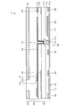
- FIG. 2 is a cross-sectional view taken along line AA of the liquid crystal display device shown in FIG. It is a top view of the liquid crystal display device which concerns on other embodiment of this invention.
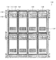
- FIG. 4 is a cross-sectional view of the liquid crystal display device shown in FIG. It is a figure which shows the comparative example with respect to the liquid crystal display device which concerns on this Embodiment.
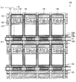
- FIG. 1 is a plan view of a liquid crystal display device according to an embodiment of the present invention.
- a TFT thin film transistor array substrate
- FIG. 1 only the active matrix substrate (hereinafter referred to as a TFT (thin film transistor) array substrate) 100 side is illustrated for convenience of description, and the liquid crystal layer 300 and the counter substrate 200 are omitted.
- TFT thin film transistor
- FIG. 2 is a cross-sectional view taken along line AA of the liquid crystal display device shown in FIG.
- the liquid crystal layer 300 and the counter substrate 200 are also illustrated. That is, as shown in FIG. 2, the liquid crystal display device 11 according to the present embodiment has a configuration in which a liquid crystal layer 300 is sandwiched between a TFT array substrate 100 and a counter substrate 200 facing the TFT array substrate 100. is there.
- the TFT array substrate 100 will be described.
- the TFT array substrate 100 includes a pixel electrode 106 and a photosensor element (photosensor) 107 as shown in FIG.
- the pixel electrode 106 and the photo sensor element 107 are arranged in a matrix on an insulating substrate (not shown), and one pixel electrode 106 and one photo sensor element 107 constitute one pixel. That is, the TFT array substrate 100 has a configuration in which one photosensor element 107 is further incorporated in one pixel in addition to one pixel electrode 106.
- the TFT array substrate (active matrix substrate) preferably has switching elements for independently driving pixels arranged in a matrix.
- the pixel electrode 106 is electrically connected to the drain electrode 112 of the TFT 104 formed at the intersection of the source bus line 101 and the gate bus line 102 orthogonal to the source bus line 101 via the contact hole 113. Yes.
- the drain electrode 112 is electrically connected to the silicon layer 110.
- a CS bus line 103 and a photosensor wiring 109 are formed substantially parallel to the gate bus line 102.
- the CS bus line 103 forms a CS electrode 105 for each pixel, and the CS electrode 105 and the silicon layer 110 constitute an auxiliary capacitor.
- the photosensor wiring 109 is a wiring for transmitting a signal for controlling a sensing circuit including the photosensor element 107 and the TFT 104 connected to the photosensor element 107.
- the photo sensor element 107 is a photoelectric conversion element that receives light and converts it into a current.
- the photo sensor element 107 includes a photodiode, and supplies a current corresponding to the amount of received light to the photo sensor wiring 109. ing. This makes it possible to detect the amount of received light for each pixel.
- a layer (second layer) including the first shield electrode 108 is provided between the layer including the photosensor element 107 (first layer) and the layer including the pixel electrode 106 (third layer). It has been.
- the first shield electrode 108 is formed so as to cover the photosensor element 107 and is insulated from the pixel electrode 106. Therefore, the first shield electrode 108 has a function of suppressing the influence of noise caused by potential fluctuation or the like in the pixel electrode 106 with respect to the photosensor element 107.
- the first shield electrode 108 is formed of a transparent electrode integrally formed along the photosensor wiring 109 so as to cover a plurality of adjacent photosensor elements 107.
- the first shield electrode 108 is connected to a power source (not shown) so that a predetermined potential is always applied.
- the first shield electrode 108 in the present embodiment is preferably transparent. Further, the electrode single membrane transmittance of the first shield electrode 108 is preferably 80% or more in the wavelength region of 400 to 700 nm which is the visible light region.
- the first shield electrode 108 is transparent, a portion corresponding to the photosensor element 107 can also contribute to transmissive display. In addition, since it is not necessary to provide an opening in a portion corresponding to the photosensor element 107 in the first shield electrode 108, the influence of electrical noise can be reduced more reliably. Further, since the photosensor element 107 can be completely covered with the first shield electrode 108, it is not necessary to further provide a shield electrode such as a transparent electrode in the third layer including the pixel electrode 106. Can be widely arranged. Accordingly, the liquid crystal molecules can be efficiently aligned, light leakage due to disorder of the alignment of the liquid crystal molecules can be prevented, and the aperture ratio can be increased.
- the pixel electrode 106 is preferably formed so as to cover the first shield electrode 108.
- the liquid crystal molecules on the photosensor element 107 are normally driven to contribute to transmissive display. Can be made.
- the TFT array substrate 100 is a surface (first layer) on the surface opposite to the formation surface of the pixel electrode 106 (pixel electrode formation surface), that is, on the insulating substrate (not shown) in the lowermost layer.
- the first insulating film 111a is stacked on the first insulating film 111a so as to cover the photosensor element 107 and the silicon layer 110 formed by patterning or the like on one layer), and each wiring (gate bus line 102, A photosensor wiring 109) and a CS electrode 105 are formed. Further, a second insulating film 111b is laminated so as to cover each of the wirings and the CS electrode 105.
- the drain electrode 112 constituting the TFT 104 is formed on the second insulating film 111b.
- the drain electrode 112 is electrically connected to the silicon layer 110 existing immediately below the pixel electrode 106 through a contact hole 111e formed in the first insulating film 111a and the second insulating film 111b.
- a third insulating film 111c is laminated on the second insulating film 111b so as to cover the drain electrode 112.
- a first shield electrode 108 is formed on the layer (second layer) on the third insulating film 111c.
- a fourth insulating film 111d is laminated on the third insulating film 111c so as to cover the first shield electrode 108.
- a pixel electrode 106 is formed on the layer (third layer) on the fourth insulating film 111d. The pixel electrode 106 is electrically connected to the drain electrode 112 through a contact hole 113 formed in the third insulating film 111c and the fourth insulating film 111d.
- a light shield 121 having a light shield opening 121a is formed at a position corresponding to the photosensor element 107 on the upper surface of the pixel electrode 106.
- the opening width of the light shielding body opening 121a is smaller than the opening width of the color filter layer opening 201a in the color filter layer 201 of the counter substrate 200 described later, and larger than the width of the light receiving portion of the photosensor element 107. Thereby, it is possible to prevent stray light from entering the photo sensor element 107.
- the position of the light shielding body 121 is not limited to the upper surface of the pixel electrode 106, but may be a position where stray light can be prevented from entering the photosensor element 107.
- it may be on the first shield electrode 108 or may be provided on the counter substrate 200 described later.
- the counter substrate 200 is provided with a transparent insulating substrate (not shown) on the outermost surface, and a color filter layer 201 is formed on the insulating substrate.
- the color filter layer 201 is set to RGB so as to correspond to each pixel of the TFT array substrate 100.
- a color filter layer opening 201a is formed in a portion corresponding to the photosensor element 107 of the TFT array substrate 100.
- a counter electrode (not shown) is formed at a position facing the pixel electrode 106 on the surface of the color filter layer 201 on the liquid crystal layer 300 side, that is, the surface facing the pixel electrode formation surface of the TFT array substrate 100. Yes.
- the counter substrate 200 has an alignment film for controlling the alignment of the liquid crystal formed on the counter electrode on the liquid crystal layer 300 side.
- An alignment film for controlling the alignment of the liquid crystal is also formed on the electrode 106.
- the liquid crystal display device 11 described above is a transmissive liquid crystal display device, but the present invention can be applied to a transflective liquid crystal display device in addition to such a transmissive liquid crystal display device. .
- the liquid crystal display device 11 includes a display panel in which the photosensor element 107 serving as a photosensor is built in a pixel.
- the pixel includes a first layer including the photosensor element 107, a second layer including the first shield electrode 108, and a third layer including the pixel electrode 106.
- the second layer is provided between the first layer and the third layer, the first shield electrode 108 covers the photosensor element 107, and
- the pixel electrode 106 is insulated from the pixel electrode 106.
- the first shield electrode 108 that covers the photosensor element 107 is provided between the photosensor element 107 and the pixel electrode 106, and the first shield electrode 108 is insulated from the pixel electrode 106. Therefore, the influence of electrical noise due to potential fluctuation in the pixel electrode 106 is blocked by the first shield electrode 108 and does not reach the photosensor element 107.
- the pixel electrode 106 and the first shield electrode 108 are provided in different layers, the pixel electrode 106 and the first shield electrode 108 can be overlapped with each other, so that the transmission aperture area can be increased. In addition, it is possible to prevent light leakage due to disordered alignment of liquid crystal molecules.
- the influence of optical noise on the photosensor element 107 due to the wraparound of light is reduced. Therefore, the influence of electrical and optical noise on the photosensor element 107 can be reduced, and the sensitivity of the photosensor element 107 can be prevented from being lowered. As a result, the sensitivity of the photosensor element 107, which is a photosensor, can be improved as compared with a conventional display panel with a built-in photosensor. Further, since the alignment accuracy is high, it is not necessary to take a margin more than necessary.
- the display device according to the present invention when applied to a liquid crystal display device with a built-in optical sensor touch panel, the sensitivity of the optical sensor is good, so that the recognition accuracy is improved in the touch operation by the user, and the operability of the touch panel is improved. be able to.
- FIG. 3 is a plan view of a liquid crystal display device according to another embodiment of the present invention
- FIG. 4 is a cross-sectional view of the liquid crystal display device shown in FIG.
- the first shield electrode 108a is opaque and the first shield electrode opening 108c is provided, the second shield electrode 108b is provided, and the light shield 121 is provided.
- the point which is not provided is different from the first embodiment, and the rest is configured similarly to the first embodiment. Therefore, in this embodiment, only points different from the first embodiment will be described, and members having the same configuration are denoted by the same member numbers, and description thereof is omitted.
- the first shield electrode 108a in the present embodiment is opaque, and is provided with a first shield electrode opening 108c as shown in FIG.
- opaque means that the transmittance is 1% or less, more preferably 0.1% or less.
- first shield electrode 108a in the present embodiment it is preferable to use a metal having both electrical conductivity and light shielding properties, and although not particularly limited, for example, tantalum (Ta), titanium (Ti), aluminum (Al ) Or the like can be used.
- first shield electrode 108a that can block infrared light. With the above configuration, infrared light can be further blocked from the photosensor element 107.
- the first shield electrode 108a since the first shield electrode 108a is opaque, it also serves to shield the peripheral edge of the light receiving portion of the photosensor element 107, and the photosensor element 107 is affected by liquid crystal alignment disorder. The influence of optical noise due to light leakage, light wraparound, etc. can be further reduced.
- the first shield electrode opening 108c is provided at a position corresponding to the light receiving portion of the photosensor element 107 in the first shield electrode 108a. By providing the first shield electrode opening 108 c, the first shield electrode 108 a does not prevent the photosensor element 107 from receiving light.
- the second shield electrode 108 b covering the first shield electrode opening 108 c is provided in the same layer as the pixel electrode 106.
- the second shield electrode 108b is transparent and insulated from the pixel electrode 106.
- the electrode single membrane transmittance of the second shield electrode 108b is preferably 80% or more in the wavelength region of 400 to 700 nm, which is the visible light region.
- the second shield electrode 108b covers the first shield electrode opening 108c and is insulated from the pixel electrode 106, the influence of electrical noise on the photosensor element 107 can be reduced.
- the second shield electrode 108b is transparent, it does not prevent the photosensor element 107 from receiving light.
- the second shield electrode 108b and the pixel electrode 106 are formed in the same layer as in this embodiment, the second shield electrode 108b and the pixel electrode 106 can be formed in the same process. That is, after the electrode layer to be the pixel electrode 106 and the second shield electrode 108b is formed, patterning may be performed in each pattern. Therefore, the manufacturing process of the display device can be simplified.
- the pixel electrode 106 and the second shield electrode 108b are preferably formed in the same layer as described above, but noise is shielded from the photosensor element 107. From this point of view, the pixel electrode 106 and the second shield electrode 108b need not be formed in the same layer, and may be formed in different layers.
- the second shield electrode 108b is made of a transparent electrode integrally formed along the photosensor wiring 109 so as to cover a plurality of adjacent photosensor elements 107.
- the second shield electrode 108b is connected to a power source (not shown) so that a predetermined potential is always applied.
- a constant potential is applied to the second shield electrode 108b, thereby suppressing potential fluctuation due to other signals received by the second shield electrode 108b itself, noise from the outside, and the like.
- the influence of electrical noise on the photosensor element 107 can be eliminated more reliably.
- each of the second shield electrodes 108b in each pixel is preferably electrically connected, more preferably connected to the end of the panel, and more preferably connected to a fixed potential at the end of the panel.
- the second shield electrode 108b may be formed in an island shape across one or a plurality of pixels.
- the photosensor element 107 is also affected by other signals and external noise.
- the second shield electrode 108b is electrically connected to the photosensor element 107. It is possible to disperse the influence of other signals on the sensor element 107, noise from the outside, and the like, and it becomes difficult to receive these influences.
- the second shield electrode 108b may be connected to the first shield electrode 108a via, for example, a small shield electrode. Further, the second shield electrode 108b may be formed in each first shield electrode opening 108c and connected to the nearby first shield electrode 108a. According to the above configuration, since the second shield electrode 108b and the first shield electrode 108a are electrically connected, the influence of other signals, noise from the outside, etc. on the photosensor element 107 can be further dispersed. These effects can be reduced.
- the pixel electrode 106 and the first shield electrode 108a are formed so as to overlap each other. Therefore, it is possible to widen the transmission aperture area and to prevent light leakage due to disordered alignment of liquid crystal molecules.
- the potential of the second shield electrode 108b is set so that the difference from the potential of the counter electrode is 0 V or more and 2 V or less. It is preferable that With the above configuration, since the liquid crystal alignment on the second shield electrode 108b is in a black display state, a good display quality without a reduction in contrast can be obtained.
- the potential of the second shield electrode 108b is set so that the difference from the potential of the counter electrode is 2 V or more and 10 V or less. It is preferable that With the above configuration, since the liquid crystal alignment on the second shield electrode 108b is in a black display state, a good display quality without a reduction in contrast can be obtained.
- FIG. 5 is a diagram showing a comparative example for the liquid crystal display device according to the present embodiment.
- the TFT array substrate 1100 in the liquid crystal display device of this comparative example shown in FIG. 5 has the same configuration as the TFT array substrate 100 in the first embodiment shown in FIG. 1 except that the first shield electrode 108 is not provided. is there.
- the member numbers have been changed to 1000s, the functions are the same.
- the source bus line 1101 corresponds to the source bus line 101
- the gate bus line 1102 corresponds to the gate bus line 102
- the CS bus line 1103 corresponds to the CS bus line 103
- the TFT 1104 corresponds to the TFT 104.
- the CS electrode 1105 corresponds to the CS electrode 105
- the pixel electrode 1106 corresponds to the pixel electrode 106
- the photosensor element 1107 corresponds to the photosensor element 107.
- the photosensor element 1107 in the pixel is covered with a pixel electrode 1106 that is a transparent electrode, the photosensor element 1107 is easily affected by noise due to potential fluctuation of the pixel electrode 1106. For this reason, since the N (noise) component of S / N indicating the sensitivity of the photosensor element 1107 increases, the sensitivity of the photosensor element 1107 decreases.
- the first shield electrode 108 is provided between the photosensor element 107 and the pixel electrode 106 in the TFT array substrate 100. Since the pixel electrode 106 is formed in an insulated state, the potential fluctuation of the pixel electrode 106 is blocked by the first shield electrode 108 and is not transmitted to the photosensor element 107. That is, the photo sensor element 107 is not affected by noise due to the potential fluctuation of the pixel electrode 106.
- the first shield electrode 108 is formed of a transparent electrode that is integrally formed so as to cover all adjacent photosensor elements 107, and a predetermined potential is applied to the transparent electrode. Therefore, the influence of noise due to the potential fluctuation of the pixel electrode 106 can be reliably suppressed.
- the first shield electrodes 108 and 108a are provided in a different layer from the pixel electrode 106, as shown in FIGS. . Accordingly, since the pixel electrode 106 and the first shield electrodes 108 and 108a can be overlapped, it is not necessary to provide a space between the pixel electrode 106 that contributes to display and the first shield electrodes 108 and 108a. . This makes it possible to increase the transmission aperture area and to prevent light leakage due to disordered alignment of liquid crystal molecules.
- the first shield electrode 108a since the first shield electrode 108a is opaque, it also serves to shield the peripheral portion of the light receiving portion of the photosensor. As a result, the optical sensor is less affected by optical noise due to light leakage due to alignment disorder of the liquid crystal and light wraparound. In particular, when a metal or the like that can block infrared light is used for the first shield electrode 108a, infrared light can also be blocked from the optical sensor.
- Applicable to display devices having a photosensor in a pixel and particularly applicable to a display device that requires improved sensitivity of a photosensor such as a liquid crystal display panel with a photosensor touch panel and a liquid crystal display panel with a photosensor scanner function. .
- Liquid crystal display device 100 TFT array substrate 101 Source bus line 102 Gate bus line 103 CS bus line 104 TFT 105 CS electrode 106 Pixel electrode 107 Photosensor element (photosensor) 108, 108a First shield electrode 108b Second shield electrode 108c First shield electrode opening (opening) 109 Photosensor wiring 110 Silicon layer 111a First insulating film 111b Second insulating film 111c Third insulating film 111d Fourth insulating film 111e Contact hole 112 Drain electrode 113 Contact hole 121 Light shield 121a Light shield opening 200 Counter substrate 201 Color Filter layer 201a Color filter layer opening 300 Liquid crystal layer
Landscapes
- Physics & Mathematics (AREA)
- Nonlinear Science (AREA)
- Liquid Crystal (AREA)
- Engineering & Computer Science (AREA)
- Microelectronics & Electronic Packaging (AREA)
- Mathematical Physics (AREA)
- Chemical & Material Sciences (AREA)
- Crystallography & Structural Chemistry (AREA)
- General Physics & Mathematics (AREA)
- Optics & Photonics (AREA)
- Position Input By Displaying (AREA)
Abstract
本発明は、画素内に光センサを内蔵した表示パネルを備えた表示装置に関する。本発明の表示装置は、画素内に光センサであるフォトセンサ素子(107)を内蔵した表示パネルを備え、上記画素は、上記フォトセンサ素子(107)を備える第1のレイヤーと、第1のシールド電極(108)を備える第2のレイヤーと、画素電極(106)を備える第3のレイヤーとを含む。上記第2のレイヤーは、上記第1のレイヤーと上記第3のレイヤーとの間に設けられ、上記第1のシールド電極(108)は、上記フォトセンサ素子(107)を覆っており、かつ上記画素電極(106)と絶縁されている。本発明によると、光センサに対して電気的ノイズの影響を小さくして、光センサの感度の低下防止を図ることができる。本発明は、光センサタッチパネル内蔵液晶表示パネル、光センサスキャナ機能内蔵液晶表示パネルに適用できる。
Description
本発明は、画素内に光センサを内蔵した表示パネルを備えた表示装置に関するものである。
従来、画素内に光センサを内蔵した表示パネルを備えた表示装置が提案されている。
上記表示装置において光センサとして、一般的にフォトダイオードが使用される。このフォトダイオードの感度は、一般に、S(信号)/N(ノイズ)で示される。つまり、S/Nの値が大きければ感度がよいことになる。
画素内に光センサを内蔵した表示パネルにおいて、光センサの感度を向上させる方法として、例えば特許文献1には、一つの画素内に2つのフォトダイオードを設けることで光電流を増大させてS(信号)/N(ノイズ)を向上させる技術が開示されている。つまり、特許文献1に開示された技術では、フォトダイオードの感度を示すS/NのうちS(信号)を示す光電流を増大させて感度を向上させている。
ところで、上記表示装置において光センサとして使用されるフォトダイオードは、画素内の画素電極における電位変動の影響によるノイズ(電気的ノイズ)を受けやすい。この場合、フォトダイオードの感度を示すS/Nのうち、分母であるN(ノイズ)の値が大きくなるので、感度低下を招くという問題が生じる。
例えば、特許文献1では、フォトダイオードの感度を向上させるために、画素内に2つのフォトダイオードを設けて光電流(S)を増大させているが、フォトダイオードの数が増えた分、受けるノイズ(N)も多くなるので、結果として、光センサとしての感度が低下するという問題が生じる。
本発明は、上述の問題点に鑑みてなされたものであり、その目的は、光センサに対して電気的ノイズの影響を小さくして、光センサの感度の低下防止を図ることのできる表示装置を実現することにある。
本発明に係る表示装置は、上記課題を解決するために、画素内に光センサを内蔵した表示パネルを備え、上記画素は、上記光センサを備える第1のレイヤーと、第1のシールド電極を備える第2のレイヤーと、画素電極を備える第3のレイヤーとを含み、上記第2のレイヤーは、上記第1のレイヤーと上記第3のレイヤーとの間に設けられ、上記第1のシールド電極は、上記光センサを覆っており、かつ上記画素電極と絶縁されていることを特徴としている。
本発明に係るアクティブマトリクス基板は、マトリクス状に配された画素を、それぞれ独立して駆動するためのスイッチング素子を有するアクティブマトリクス基板において、上記画素は、光センサを備える第1のレイヤーと、第1のシールド電極を備える第2のレイヤーと、画素電極を備える第3のレイヤーとを含み、上記第2のレイヤーは、上記第1のレイヤーと上記第3のレイヤーとの間に設けられ、上記第1のシールド電極は、上記光センサを覆っており、かつ上記画素電極と絶縁されていることを特徴としている。
上記の構成によれば、光センサと画素電極との間に、光センサを覆う第1のシールド電極が設けられ、この第1のシールド電極が画素電極と絶縁状態にあるので、画素電極における電位変動による電気的ノイズの影響が、第1のシールド電極によって遮断され、光センサには及ばない。また、画素電極と第1のシールド電極とを別のレイヤーに備えているので、画素電極と第1のシールド電極とを重畳させることができるため、透過開口面積を広くすることが可能になるとともに、液晶分子の配向乱れによる光漏れを防ぐことができる。従って、光センサに対して電気的ノイズの影響を小さくすることができ、光センサの感度の低下防止を図ることができ、この結果、従来の光センサ内蔵の表示パネルに比べて光センサの感度向上を図ることができる。
従って、本発明に係る表示装置またはアクティブマトリクス基板を光センサタッチパネル内蔵液晶表示装置に適用した場合に、光センサの感度がよいので、ユーザによるタッチ操作においてその認識精度がよくなり、タッチパネルの操作性の向上を図ることができる。
また、上記第1のシールド電極には、所定の電位が印加されていることが好ましい。
上記の構成によれば、第1のシールド電極に一定の電位が印加されていることで、第1のシールド電極自体が受ける他の信号、外部からのノイズなどによる電位変動を抑えることができ、光センサに対する電気的ノイズの影響をより確実に無くすことができる。つまり、この場合、第1のシールド電極が光センサと画素電極との間のレイヤーに備えられていることによって、第1のシールド電極が光センサへのノイズ進入を防止する機能を果たす。
また、上記第1のシールド電極は透明であることが好ましい。
また、上記第1のシールド電極の電極単膜透過率は、400~700nmの波長領域において80%以上であることが好ましい。
上記の構成であれば、第1のシールド電極が透明であるため、光センサに相当する部分も透過表示に寄与させることができる。また、第1のシールド電極における光センサに相当する部分に、開口部を設ける必要がないので、電気的ノイズの影響をより確実に小さくすることが出来る。また、第1のシールド電極で光センサを完全に覆うことができるので、画素電極を備える第3のレイヤーに透明電極などをさらに設ける必要がないため、画素電極を広く配置することができ、したがって液晶分子を効率よく配向させることができ、液晶分子の配向乱れによる光漏れを防ぐとともに、開口率を上げることができる。
また、上記画素電極は、上記第1のシールド電極を覆っていることが好ましい。
上記の構成であれば、光センサを覆っている第1のシールド電極を、画素電極がさらに覆っているため、光センサ上の液晶分子を通常駆動させ、透過表示に寄与させることができる。
また、上記光センサの受光部の周縁部を遮光する遮光体が設けられていることが好ましい。
上記の構成であれば、光センサの受光部の周縁部を遮光することができるので、光センサに対して迷光が侵入するのを阻止することができる。
また、上記第1のシールド電極は、不透明であることが好ましい。
上記の構成によれば、第1のシールド電極が不透明であるため、光センサの受光部の周縁部を遮光する役割をも果たし、光センサに対して、液晶の配向乱れによる光漏れ、光の回り込みなどによる光学的ノイズの影響をより小さくすることができる。また、例えば赤外光を遮断できる金属等を用いる場合には、光センサに対して赤外光をも遮断することができる。
また、上記第1のシールド電極は、上記光センサの受光部に対応する位置に開口部を設けていることが好ましい。
上記の構成によれば、第1のシールド電極が、光センサの受光部に対応する位置に開口部を設けているため、光センサの受光を妨げない。また、第1のシールド電極は、光センサの近傍に設けられるため、アラインメント精度が高いために、開口部においてマージンを必要以上にとらずに済む。
また、上記開口部を覆う第2のシールド電極をさらに備えており、上記第2のシールド電極は、透明であり、かつ上記画素電極と絶縁されていることが好ましい。
また、上記第2のシールド電極の電極単膜透過率は、400~700nmの波長領域において80%以上であることが好ましい。
上記の構成によれば、第1のシールド電極における開口部を、画素電極と絶縁されている第2のシールド電極が覆っているため、光センサに対する電気的ノイズの影響を小さくすることが出来る。また、第2のシールド電極は透明であるため、光センサの受光を妨げない。
また、上記第2のシールド電極は、上記第3のレイヤーに備えられていることが好ましい。
上記の構成によれば、第2のシールド電極と画素電極とが同一レイヤーに形成されているので、第2のシールド電極と画素電極とを同じ工程において作ることができる。すなわち、画素電極及び第2のシールド電極となる電極層を形成した後、それぞれ所定のパターンにパターニングすればよい。従って、表示装置の製造工程を簡略化することができる。
また、上記第2のシールド電極には、所定の電位が印加されていることが好ましい。
上記の構成によれば、第2のシールド電極に一定の電位が印加されていることで、第2のシールド電極自体が受ける他の信号、外部からのノイズなどによる電位変動を抑えることができ、光センサに対する電気的ノイズの影響をより確実に無くすことができる。
また、各画素における上記第2のシールド電極の各々が電気的に接続されていることが好ましい。
光センサに対しては、画素電極による電気的ノイズ以外に、他の信号、外部からのノイズなどの影響もあるが、上記の構成によれば、第2のシールド電極同士が電気的に接続されることで、光センサに対する他の信号、外部からのノイズなどの影響を分散させることができ、これらの影響を受け難くなる。
また、上記第2のシールド電極は、上記第1のシールド電極に接続していることが好ましい。
上記の構成によれば、第2のシールド電極と第1のシールド電極とが電気的に接続されるため、光センサに対する他の信号、外部からのノイズなどの影響をさらに分散させることができ、これらの影響をより小さくすることができる。
また、上記表示パネルは、ノーマリーブラックモードを採用しており、上記画素電極が形成された基板の画素電極形成面に対向する面に対向電極が設けられた対向基板を備え、上記第2のシールド電極の電位は、上記対向電極の電位との差が0V以上2V以下となるように設定されていることが好ましい。
上記の構成であれば、表示パネルがノーマリーブラックモードを採用しているとき、第2のシールド電極の電位と対向電極の電位との差が0V以上2V以下に設定されていることで、第2のシールド電極上における液晶の配向が黒表示状態になるので、コントラストの低下を伴わない良好な表示品位が得られる。
また、上記表示パネルは、ノーマリーホワイトモードを採用しており、上記画素電極が形成された基板の画素電極形成面に対向する面に対向電極が設けられた対向基板を備え、上記第2のシールド電極の電位は、上記対向電極の電位との差が2V以上10V以下となるように設定されていることが好ましい。
上記の構成であれば、表示パネルがノーマリーホワイトモードを採用しているとき、第2のシールド電極の電位と対向電極の電位との差が2V以上10V以下に設定されていることで、第2のシールド電極上における液晶の配向が黒表示状態になるので、コントラストの低下を伴わない良好な表示品位が得られる。
本発明に係る表示装置は、以上のように、画素内に光センサを内蔵した表示パネルを備え、上記画素は、上記光センサを備える第1のレイヤーと、第1のシールド電極を備える第2のレイヤーと、画素電極を備える第3のレイヤーとを含み、上記第2のレイヤーは、上記第1のレイヤーと上記第3のレイヤーとの間に設けられ、上記第1のシールド電極は、上記光センサを覆っており、かつ上記画素電極と絶縁されているので、光センサの感度の低下防止を図ることができ、この結果、従来の光センサ内蔵の表示パネルに比べて光センサの感度向上を図ることができる。
従って、本発明に係る表示装置を光センサタッチパネル内蔵液晶表示装置に適用した場合に、光センサの感度がよいので、ユーザによるタッチ操作におけるその認識精度がよくなり、タッチパネルの操作性の向上を図ることができるという効果を奏する。
本発明の他の目的、特徴、及び優れた点は、以下に示す記載によって十分分かるであろう。また、本発明の利点は、添付図面を参照した次の説明で明白になるであろう。
本発明は以下の各実施形態に限定されるものではなく、請求項に示した範囲で種々の変更が可能であり、異なる実施形態にそれぞれ開示される技術的手段を適宜組み合わせて得られる実施形態についても本発明の技術的範囲に含まれる。
〔第1の実施形態〕
本発明の一実施形態について説明すれば以下の通りである。なお、本実施の形態では、本発明の表示装置を、光センサタッチパネル内蔵の液晶表示装置に適用した例について説明する。
本発明の一実施形態について説明すれば以下の通りである。なお、本実施の形態では、本発明の表示装置を、光センサタッチパネル内蔵の液晶表示装置に適用した例について説明する。
本実施の形態に係る液晶表示装置の全体構成について、図1及び図2を参照しながら以下に説明する。
図1は、本発明の一実施形態に係る液晶表示装置の平面図である。なお、図1では、説明の便宜上、アクティブマトリクス基板(以下、TFT(Thin Film Transistor)アレイ基板と称する)100側のみを記載し、液晶層300及び対向基板200については省略している。
図2は、図1に示す液晶表示装置のA-A線矢視断面図である。なお、図2では、TFTアレイ基板100に加えて、液晶層300及び対向基板200についても図示している。すなわち、図2に示すように、本実施の形態に係る液晶表示装置11は、TFTアレイ基板100と、このTFTアレイ基板100に対向する対向基板200との間に液晶層300を挟持した構成である。
まず、TFTアレイ基板100について説明する。
TFTアレイ基板100は、図1に示すように、画素電極106及びフォトセンサ素子(光センサ)107を備えている。
画素電極106及びフォトセンサ素子107は、図示しない絶縁基板上に、マトリクス状に配されており、一つの画素電極106と一つのフォトセンサ素子107とによって一つの画素を構成している。つまり、TFTアレイ基板100は、一つの画素内に、一つの画素電極106の他に、一つのフォトセンサ素子107をさらに内蔵した構成となっている。
なお、TFTアレイ基板(アクティブマトリクス基板)は、マトリクス状に配された画素をそれぞれ独立して駆動するためのスイッチング素子を有することが好ましい。
画素電極106は、ソースバスライン101と、このソースバスライン101に直交するゲートバスライン102との交差部に形成されたTFT104のドレイン電極112に、コンタクトホール113を介して電気的に接続されている。
ドレイン電極112は、シリコン層110と電気的に接続されている。
ゲートバスライン102と略平行に、CSバスライン103とフォトセンサ用配線109とが形成されている。
CSバスライン103は、画素毎にCS電極105を形成し、このCS電極105とシリコン層110とで補助容量を構成している。
フォトセンサ用配線109は、フォトセンサ素子107と、フォトセンサ素子107に接続されたTFT104とからなるセンシング回路を制御する信号を伝送する配線である。
フォトセンサ素子107は、光を受光して電流に変換する光電変換素子であり、例えばフォトダイオードからなり、受光した光の量に応じた量の電流をフォトセンサ用配線109に供給するようになっている。これにより、画素毎に、受光量を検出することが可能となる。
フォトセンサ素子107を備えるレイヤー(第1のレイヤー)と、画素電極106を備えるレイヤー(第3のレイヤー)との間には、第1のシールド電極108を備えるレイヤー(第2のレイヤー)が設けられている。この第1のシールド電極108は、フォトセンサ素子107を覆うように形成されており、かつ画素電極106と絶縁されている。従って、第1のシールド電極108は、フォトセンサ素子107に対して、画素電極106における電位変動等によって生じるノイズの影響を抑制する機能を果たすようになっている。
第1のシールド電極108は、隣接する複数のフォトセンサ素子107を覆うように、フォトセンサ用配線109に沿って一体的に形成された透明電極からなっている。この第1のシールド電極108は、図示しない電源に接続されており、所定の電位が常に印加されるようになっている。
本実施の形態における第1のシールド電極108は、透明であることが好ましい。また、第1のシールド電極108の電極単膜透過率は、可視光領域である400~700nmの波長領域において80%以上であることが好ましい。
上記の構成であれば、第1のシールド電極108が透明であるため、フォトセンサ素子107に相当する部分も透過表示に寄与させることができる。また、第1のシールド電極108におけるフォトセンサ素子107に相当する部分に、開口部を設ける必要がないので、電気的ノイズの影響をより確実に小さくすることが出来る。また、第1のシールド電極108でフォトセンサ素子107を完全に覆うことができるので、画素電極106を備える第3のレイヤーに透明電極などのシールド電極をさらに設ける必要がないため、画素電極106を広く配置することができる。従って液晶分子を効率よく配向させることができ、液晶分子の配向乱れによる光漏れを防ぐとともに、開口率を上げることができる。
また、図1に示すように、画素電極106は、第1のシールド電極108を覆うように形成されていることが好ましい。上記の構成であれば、フォトセンサ素子107を覆っている第1のシールド電極108を、画素電極106がさらに覆っているため、フォトセンサ素子107上の液晶分子を通常駆動させ、透過表示に寄与させることができる。
TFTアレイ基板100は、図2に示すように、画素電極106の形成面(画素電極形成面)とは反対側の面、すなわち最下層にある絶縁性基板(図示せず)上の層(第1のレイヤー)にパターニング等により形成されたフォトセンサ素子107及びシリコン層110を覆うように、第1絶縁膜111aが積層され、この第1絶縁膜111a上に、各配線(ゲートバスライン102、フォトセンサ用配線109)及びCS電極105が形成されている。さらに、上記の各配線及びCS電極105を覆うように、第2絶縁膜111bが積層されている。
第2絶縁膜111b上にはTFT104を構成するドレイン電極112が形成されている。このドレイン電極112は、第1絶縁膜111a及び第2絶縁膜111bに形成されたコンタクトホール111eを介して、画素電極106の直下に存在するシリコン層110と電気的に接続されている。
さらに、第2絶縁膜111b上には、ドレイン電極112を覆うように、第3絶縁膜111cが積層されている。第3絶縁膜111c上の層(第2のレイヤー)には、第1のシールド電極108が形成されている。
さらに、第3絶縁膜111c上には、第1のシールド電極108を覆うように、第4絶縁膜111dが積層されている。第4絶縁膜111d上の層(第3のレイヤー)には、画素電極106が形成されている。この画素電極106は、第3絶縁膜111c及び第4絶縁膜111dに形成されたコンタクトホール113を介してドレイン電極112に電気的に接続されている。
また、画素電極106の上面のフォトセンサ素子107に相当する位置に、遮光体開口部121aを有する遮光体121が形成されている。遮光体開口部121aの開口幅は、後述する対向基板200のカラーフィルタ層201におけるカラーフィルタ層開口部201aの口幅よりも小さく、フォトセンサ素子107の受光部の幅よりも大きい。これにより、フォトセンサ素子107に対して迷光が侵入するのを阻止することができる。
なお、遮光体121の位置は、画素電極106の上面には限らず、フォトセンサ素子107に対して迷光が侵入するのを阻止できる位置であればよい。例えば、第1のシールド電極108上であってもよいし、後述する対向基板200に設けられていてもよい。
次に、対向基板200について説明する。
対向基板200は、図2に示すように、最表面には図示しない透明な絶縁性基板が配され、その絶縁性基板上にカラーフィルタ層201が形成されている。このカラーフィルタ層201は、TFTアレイ基板100の各画素に対応するようにRGB設定されている。
また、カラーフィルタ層201は、TFTアレイ基板100のフォトセンサ素子107に相当する部分にカラーフィルタ層開口部201aが形成されている。
さらに、カラーフィルタ層201の液晶層300側の面、すなわちTFTアレイ基板100における画素電極形成面に対向する面には、画素電極106と対向する位置に対向電極(図示せず)が形成されている。
なお、図2において図示していないが、対向基板200には、液晶層300側の対向電極上に液晶の配向を制御するための配向膜が形成されており、同じく、TFTアレイ基板100の画素電極106上にも液晶の配向を制御するための配向膜が形成されている。
以上説明した液晶表示装置11は、透過型の液晶表示装置であるが、本発明は、このような透過型の液晶表示装置以外にも、半透過型の液晶表示装置にも適用することができる。
以上のように、本実施の形態に係る液晶表示装置11は、画素内に光センサとなるフォトセンサ素子107を内蔵した表示パネルを備えている。上記画素は、上記フォトセンサ素子107を備える第1のレイヤーと、第1のシールド電極108を備える第2のレイヤーと、画素電極106を備える第3のレイヤーとを含んでいる。そして、上記第2のレイヤーは、上記第1のレイヤーと上記第3のレイヤーとの間に設けられており、上記第1のシールド電極108は、上記フォトセンサ素子107を覆っており、かつ上記画素電極106と絶縁されている構成となっている。
上記の構成によれば、フォトセンサ素子107と画素電極106との間に、フォトセンサ素子107を覆う第1のシールド電極108が設けられ、この第1のシールド電極108が画素電極106と絶縁状態にあるので、画素電極106における電位変動による電気的ノイズの影響が、第1のシールド電極108によって遮断され、フォトセンサ素子107には及ばない。また、画素電極106と第1のシールド電極108とを別のレイヤーに備えているので、画素電極106と第1のシールド電極108とを重畳させることができるため、透過開口面積を広くすることが可能になるとともに、液晶分子の配向乱れによる光漏れを防ぐことができる。さらに、第1のシールド電極108を備えることにより、光の回り込みによる光学的ノイズのフォトセンサ素子107への影響が小さくなる。従って、フォトセンサ素子107に対して電気的および光学的ノイズの影響を小さくすることができ、フォトセンサ素子107の感度の低下防止を図ることができる。その結果、従来の光センサ内蔵の表示パネルに比べて光センサであるフォトセンサ素子107の感度向上を図ることができる。また、アラインメント精度が高いために、マージンを必要以上にとらずに済む。
従って、本発明に係る表示装置を光センサタッチパネル内蔵液晶表示装置に適用した場合に、光センサの感度がよいので、ユーザによるタッチ操作においてその認識精度がよくなり、タッチパネルの操作性の向上を図ることができる。
〔第2の実施形態〕
次に、本発明の他の実施形態について、図3及び図4を参照しながら以下に説明する。
次に、本発明の他の実施形態について、図3及び図4を参照しながら以下に説明する。
図3は、本発明の他の実施形態に係る液晶表示装置の平面図であり、図4は、図3に示す液晶表示装置のB-B線矢視断面図である。
第2の実施形態においては、第1のシールド電極108aが不透明でありかつ第1のシールド電極開口部108cを設けている点、第2のシールド電極108bを備えている点、及び遮光体121を備えていない点、が第1の実施形態と異なっており、他は第1の実施形態と同様に構成されている。よって、本実施形態では、第1の実施形態と異なる点のみについて説明し、同様の構成の部材には同じ部材番号を付してその説明は省略する。
本実施の形態における第1のシールド電極108aは、不透明であり、かつ図3に示すように、第1のシールド電極開口部108cを設けている。
本明細書において「不透明」であるとは、透過率が1%以下、より好ましくは0.1%以下であることを言う。
本実施の形態における第1のシールド電極108aには、導電性と遮光性とを兼ね備えている金属を用いることが好ましく、特に限定されないが、例えばタンタル(Ta)、チタン(Ti)、アルミニウム(Al)等の金属を用いることができる。また、第1のシールド電極108aに、赤外光を遮断することができるものを用いることが好ましい。上記の構成であれば、フォトセンサ素子107に対して、さらに赤外光をも遮断することができる。
本実施の形態においては、第1のシールド電極108aが不透明であるため、フォトセンサ素子107の受光部の周縁部を遮光する役割をも果たし、フォトセンサ素子107に対して、液晶の配向乱れによる光漏れ、光の回り込みなどによる光学的ノイズの影響をより小さくすることができる。
第1のシールド電極開口部108cは、第1のシールド電極108aにおける、フォトセンサ素子107の受光部に対応する位置に設けられている。第1のシールド電極開口部108cが設けられていることによって、第1のシールド電極108aは、フォトセンサ素子107の受光を妨げない。
また、第1のシールド電極開口部108cを覆う第2のシールド電極108bが、画素電極106と同一のレイヤーに備えられている。第2のシールド電極108bは、透明であり、かつ画素電極106と絶縁されている。
第2のシールド電極108bの電極単膜透過率は、可視光領域である400~700nmの波長領域において80%以上であることが好ましい。
第2のシールド電極108bは、第1のシールド電極開口部108cを覆っており、かつ画素電極106と絶縁されているため、フォトセンサ素子107に対する電気的ノイズの影響を小さくすることが出来る。また、第2のシールド電極108bは透明であるため、フォトセンサ素子107の受光を妨げない。
本実施の形態のように、第2のシールド電極108bと画素電極106とを同一レイヤーに形成する場合は、第2のシールド電極108bと画素電極106とを同じ工程において作ることができる。すなわち、画素電極106及び第2のシールド電極108bとなる電極層を形成した後、それぞれのパターンにパターニングすればよい。従って、表示装置の製造工程を簡略化することができる。
なお、製造工程の簡略化という観点からは、上記のように、画素電極106と第2のシールド電極108bとは同一レイヤーで形成するのが好ましいが、フォトセンサ素子107に対してノイズをシールドするという観点からは、画素電極106と第2のシールド電極108bとを同一レイヤーで形成する必要はなく、異なるレイヤーで形成するようにしてもよい。
第2のシールド電極108bは、図3に示すように、隣接する複数のフォトセンサ素子107を覆うように、フォトセンサ用配線109に沿って一体的に形成された透明電極からなっている。この第2のシールド電極108bは、図示しない電源に接続されており、所定の電位が常に印加されるようになっている。上記の構成によれば、第2のシールド電極108bに一定の電位が印加されていることで、第2のシールド電極108b自体が受ける他の信号、外部からのノイズなどによる電位変動を抑えることができ、フォトセンサ素子107に対する電気的ノイズの影響をより確実に無くすことができる。
なお、各画素における第2のシールド電極108bの各々が電気的に接続されていることが好ましく、さらに、パネルの端まで繋がり、パネルの端で固定電位に繋がっていることがより好ましい。また、第2のシールド電極108bは、1または複数個の画素にまたがって島状に形成されてもよい。フォトセンサ素子107に対しては画素電極による電気的ノイズ以外にも他の信号、外部からのノイズなどの影響もあるが、第2のシールド電極108b同士が電気的に接続されることにより、フォトセンサ素子107に対する他の信号、外部からのノイズなどの影響を分散させることができ、これらの影響を受け難くなる。
また、第2のシールド電極108bは、例えば小さいシールド電極等を介して、第1のシールド電極108aに接続されてもよい。また、第2のシールド電極108bは、各第1のシールド電極開口部108cに各々形成され、かつ近傍の第1のシールド電極108aに接続されてもよい。上記の構成によれば、第2のシールド電極108bと第1のシールド電極108aが電気的に接続されるため、フォトセンサ素子107に対する他の信号、外部からのノイズなどの影響をさらに分散させることができ、これらの影響をより小さくすることができる。
本実施の形態においては、画素電極106と第1のシールド電極108aとは重畳して形成されている。従って、透過開口面積を広くすることが可能になるとともに、液晶分子の配向乱れによる光漏れを防ぐことができる。
なお、本実施の形態において、例えば表示パネルがノーマリーブラックモードを採用する場合には、第2のシールド電極108bの電位は、対向電極の電位との差が0V以上2V以下となるように設定されていることが好ましい。上記の構成であれば、第2のシールド電極108b上における液晶の配向が黒表示状態になるので、コントラストの低下を伴わない良好な表示品位が得られる。
また、本実施の形態において、例えば表示パネルがノーマリーホワイトモードを採用する場合には、第2のシールド電極108bの電位は、対向電極の電位との差が2V以上10V以下となるように設定されていることが好ましい。上記の構成であれば、第2のシールド電極108b上における液晶の配向が黒表示状態になるので、コントラストの低下を伴わない良好な表示品位が得られる。
(比較例1)
ここで、本実施の形態に対する一比較例について、図5を参照して以下に説明する。
ここで、本実施の形態に対する一比較例について、図5を参照して以下に説明する。
図5は、本実施の形態に係る液晶表示装置に対する一比較例を示す図である。
図5に示す、本比較例の液晶表示装置におけるTFTアレイ基板1100は、第1のシールド電極108を備えていないこと以外、図1に示す第1の実施形態におけるTFTアレイ基板100と同じ構成である。但し、部材番号はそれぞれ1000番台に変更しているが、機能は同じである。例えば、ソースバスライン1101は、ソースバスライン101に相当し、ゲートバスライン1102は、ゲートバスライン102に相当し、CSバスライン1103は、CSバスライン103に相当し、TFT1104は、TFT104に相当し、CS電極1105は、CS電極105に相当し、画素電極1106は、画素電極106に相当し、フォトセンサ素子1107は、フォトセンサ素子107に相当している。
図5に示すように、画素内のフォトセンサ素子1107が透明電極である画素電極1106によって覆われている場合、フォトセンサ素子1107は画素電極1106の電位変動によるノイズの影響を受けやすい。このため、フォトセンサ素子1107の感度を示すS/NのN(ノイズ)成分が大きくなるので、フォトセンサ素子1107の感度が低下する。
これに対して、第1の実施形態に係る液晶表示装置11は、図1に示すように、TFTアレイ基板100においてフォトセンサ素子107と画素電極106との間に、第1のシールド電極108が、画素電極106と絶縁状態において形成されているので、該画素電極106の電位変動は第1のシールド電極108により遮断されるためフォトセンサ素子107に伝わることがない。つまり、フォトセンサ素子107は、画素電極106の電位変動によるノイズの影響を受けないようになる。
しかも、第1のシールド電極108は、図1に示すように、隣接するフォトセンサ素子107を全て覆うようにして一体的に形成された透明電極からなり、該透明電極に所定の電位が印加されているので、画素電極106の電位変動によるノイズの影響を確実に抑えることができる。
また、第1の実施形態及び第2の実施形態に係る液晶表示装置では、図1及び図3に示すように、第1のシールド電極108、108aが画素電極106と異なるレイヤーに設けられている。従って、画素電極106と第1のシールド電極108、108aとを重畳させることができるため、表示に寄与する画素電極106と、第1のシールド電極108、108aとの間にスペースを設ける必要がない。これにより、透過開口面積を広くすることが可能になるとともに、液晶分子の配向乱れによる光漏れを防ぐことができる。
さらに、第2の実施形態に係る液晶表示装置では、図3及び図4に示すように、第1のシールド電極108aが不透明であるため、光センサの受光部の周縁部を遮光する役割をも果たし、光センサに対する、液晶の配向乱れによる光漏れ、光の回り込みなどによる光学的ノイズの影響が小さい。特に、第1のシールド電極108aに、赤外光を遮断できる金属等を用いる場合には、光センサに対して赤外光をも遮断することができる。
発明の詳細な説明の項においてなされた具体的な実施形態または実施例は、あくまでも、本発明の技術内容を明らかにするものであって、そのような具体例にのみ限定して狭義に解釈されるべきものではなく、本発明の精神と次に記載する請求の範囲内で、いろいろと変更して実施することができるものである。
画素内に光センサを備えた表示装置一般に適用でき、特に、光センサタッチパネル内蔵液晶表示パネル、光センサスキャナ機能内蔵液晶表示パネルのような光センサの感度向上が求められている表示装置に適用できる。
11 液晶表示装置
100 TFTアレイ基板
101 ソースバスライン
102 ゲートバスライン
103 CSバスライン
104 TFT
105 CS電極
106 画素電極
107 フォトセンサ素子(光センサ)
108、108a 第1のシールド電極
108b 第2のシールド電極
108c 第1のシールド電極開口部(開口部)
109 フォトセンサ用配線
110 シリコン層
111a 第1絶縁膜
111b 第2絶縁膜
111c 第3絶縁膜
111d 第4絶縁膜
111e コンタクトホール
112 ドレイン電極
113 コンタクトホール
121 遮光体
121a 遮光体開口部
200 対向基板
201 カラーフィルタ層
201a カラーフィルタ層開口部
300 液晶層
100 TFTアレイ基板
101 ソースバスライン
102 ゲートバスライン
103 CSバスライン
104 TFT
105 CS電極
106 画素電極
107 フォトセンサ素子(光センサ)
108、108a 第1のシールド電極
108b 第2のシールド電極
108c 第1のシールド電極開口部(開口部)
109 フォトセンサ用配線
110 シリコン層
111a 第1絶縁膜
111b 第2絶縁膜
111c 第3絶縁膜
111d 第4絶縁膜
111e コンタクトホール
112 ドレイン電極
113 コンタクトホール
121 遮光体
121a 遮光体開口部
200 対向基板
201 カラーフィルタ層
201a カラーフィルタ層開口部
300 液晶層
Claims (17)
- 画素内に光センサを内蔵した表示パネルを備え、
上記画素は、上記光センサを備える第1のレイヤーと、第1のシールド電極を備える第2のレイヤーと、画素電極を備える第3のレイヤーとを含み、
上記第2のレイヤーは、上記第1のレイヤーと上記第3のレイヤーとの間に設けられ、
上記第1のシールド電極は、上記光センサを覆っており、かつ上記画素電極と絶縁されていることを特徴とする表示装置。 - 上記第1のシールド電極には、所定の電位が印加されていることを特徴とする請求項1に記載の表示装置。
- 上記第1のシールド電極は透明であることを特徴とする請求項1または2に記載の表示装置。
- 上記第1のシールド電極の電極単膜透過率は、400~700nmの波長領域において80%以上であることを特徴とする請求項1~3の何れか1項に記載の表示装置。
- 上記画素電極は、上記第1のシールド電極を覆っていることを特徴とする請求項1~4の何れか1項に記載の表示装置。
- 上記光センサの受光部の周縁部を遮光する遮光体が設けられていることを特徴とする請求項1~5の何れか1項に記載の表示装置。
- 上記第1のシールド電極は、不透明であることを特徴とする請求項1または2に記載の表示装置。
- 上記第1のシールド電極は、上記光センサの受光部に対応する位置に開口部を設けていることを特徴とする請求項7に記載の表示装置。
- 上記開口部を覆う第2のシールド電極をさらに備えており、
上記第2のシールド電極は、透明であり、かつ上記画素電極と絶縁されていることを特徴とする請求項8に記載の表示装置。 - 上記第2のシールド電極の電極単膜透過率は、400~700nmの波長領域において80%以上であることを特徴とする請求項9に記載の表示装置。
- 上記第2のシールド電極は、上記第3のレイヤーに備えられていることを特徴とする請求項9または10に記載の表示装置。
- 上記第2のシールド電極には、所定の電位が印加されていることを特徴とする請求項9~11の何れか1項に記載の表示装置。
- 各画素における上記第2のシールド電極の各々が電気的に接続されていることを特徴とする請求項9~12の何れか1項に記載の表示装置。
- 上記第2のシールド電極は、上記第1のシールド電極に電気的に接続されていることを特徴とする請求項9~13の何れか1項に記載の表示装置。
- 上記表示パネルは、ノーマリーブラックモードを採用しており、
上記画素電極が形成された基板の画素電極形成面に対向する面に対向電極が設けられた対向基板を備え、
上記第2のシールド電極の電位は、上記対向電極の電位との差が0V以上2V以下となるように設定されていることを特徴とする請求項9~14の何れか1項に記載の表示装置。 - 上記表示パネルは、ノーマリーホワイトモードを採用しており、
上記画素電極が形成された基板の画素電極形成面に対向する面に対向電極が設けられた対向基板を備え、
上記第2のシールド電極の電位は、上記対向電極の電位との差が2V以上10V以下となるように設定されていることを特徴とする請求項9~14の何れか1項に記載の表示装置。 - マトリクス状に配された画素を、それぞれ独立して駆動するためのスイッチング素子を有するアクティブマトリクス基板において、
上記画素は、光センサを備える第1のレイヤーと、第1のシールド電極を備える第2のレイヤーと、画素電極を備える第3のレイヤーとを含み、
上記第2のレイヤーは、上記第1のレイヤーと上記第3のレイヤーとの間に設けられ、
上記第1のシールド電極は、上記光センサを覆っており、かつ上記画素電極と絶縁されていることを特徴とするアクティブマトリクス基板。
Priority Applications (1)
| Application Number | Priority Date | Filing Date | Title |
|---|---|---|---|
| US13/128,805 US20110221722A1 (en) | 2008-11-20 | 2009-08-12 | Display device and active matrix substrate |
Applications Claiming Priority (2)
| Application Number | Priority Date | Filing Date | Title |
|---|---|---|---|
| JP2008296961 | 2008-11-20 | ||
| JP2008-296961 | 2008-11-20 |
Publications (1)
| Publication Number | Publication Date |
|---|---|
| WO2010058636A1 true WO2010058636A1 (ja) | 2010-05-27 |
Family
ID=42198075
Family Applications (1)
| Application Number | Title | Priority Date | Filing Date |
|---|---|---|---|
| PCT/JP2009/064220 Ceased WO2010058636A1 (ja) | 2008-11-20 | 2009-08-12 | 表示装置、及びアクティブマトリクス基板 |
Country Status (2)
| Country | Link |
|---|---|
| US (1) | US20110221722A1 (ja) |
| WO (1) | WO2010058636A1 (ja) |
Families Citing this family (3)
| Publication number | Priority date | Publication date | Assignee | Title |
|---|---|---|---|---|
| TWI712027B (zh) * | 2019-03-28 | 2020-12-01 | 友達光電股份有限公司 | 顯示面板 |
| CN113064307B (zh) * | 2021-03-19 | 2022-02-22 | 深圳市华星光电半导体显示技术有限公司 | 阵列基板及制作方法、显示面板 |
| CN114967246B (zh) * | 2022-05-31 | 2023-07-14 | 长沙惠科光电有限公司 | 液晶显示面板及显示装置 |
Citations (3)
| Publication number | Priority date | Publication date | Assignee | Title |
|---|---|---|---|---|
| JP2008090141A (ja) * | 2006-10-04 | 2008-04-17 | Sony Corp | 表示装置 |
| JP2009151020A (ja) * | 2007-12-19 | 2009-07-09 | Sony Corp | 表示装置及び電子機器 |
| WO2009096063A1 (ja) * | 2008-01-31 | 2009-08-06 | Sharp Kabushiki Kaisha | 表示装置、アクティブマトリクス基板 |
Family Cites Families (3)
| Publication number | Priority date | Publication date | Assignee | Title |
|---|---|---|---|---|
| US6878919B1 (en) * | 2004-04-28 | 2005-04-12 | Eastman Kodak Company | Thin lightshield process for solid-state image sensors |
| KR20060073826A (ko) * | 2004-12-24 | 2006-06-29 | 삼성전자주식회사 | 박막 트랜지스터 표시판 |
| JP2007163582A (ja) * | 2005-12-09 | 2007-06-28 | Fujifilm Corp | 液晶表示素子、及び調光材料 |
-
2009
- 2009-08-12 US US13/128,805 patent/US20110221722A1/en not_active Abandoned
- 2009-08-12 WO PCT/JP2009/064220 patent/WO2010058636A1/ja not_active Ceased
Patent Citations (3)
| Publication number | Priority date | Publication date | Assignee | Title |
|---|---|---|---|---|
| JP2008090141A (ja) * | 2006-10-04 | 2008-04-17 | Sony Corp | 表示装置 |
| JP2009151020A (ja) * | 2007-12-19 | 2009-07-09 | Sony Corp | 表示装置及び電子機器 |
| WO2009096063A1 (ja) * | 2008-01-31 | 2009-08-06 | Sharp Kabushiki Kaisha | 表示装置、アクティブマトリクス基板 |
Also Published As
| Publication number | Publication date |
|---|---|
| US20110221722A1 (en) | 2011-09-15 |
Similar Documents
| Publication | Publication Date | Title |
|---|---|---|
| JP5198474B2 (ja) | 表示装置、アクティブマトリクス基板 | |
| JP5014971B2 (ja) | ディスプレイ装置 | |
| TWI448782B (zh) | 顯示裝置 | |
| KR100961072B1 (ko) | 이미지 센싱 기능을 가지는 액정표시장치 및 그 제조방법과이를 이용한 이미지 센싱 방법 | |
| KR20090113795A (ko) | 액정 표시 장치 | |
| TWI396899B (zh) | 液晶顯示器 | |
| JP5283451B2 (ja) | 液晶表示装置 | |
| JPWO2008044369A1 (ja) | 液晶表示装置 | |
| JP5009421B2 (ja) | 液晶表示装置 | |
| JPWO2015001896A1 (ja) | 液晶表示装置 | |
| JP4924224B2 (ja) | 光検出器内蔵表示装置及び電子機器 | |
| WO2011065362A1 (ja) | 半導体装置およびその製造方法 | |
| US20190103421A1 (en) | Thin film transistor array substrate and method of producing the same | |
| JP2010056303A (ja) | 光センサ及びこの光センサを使用した液晶表示装置 | |
| JP2007304245A (ja) | 液晶表示装置 | |
| WO2010058629A1 (ja) | 液晶表示装置、電子機器 | |
| WO2018008619A1 (ja) | タッチパネル付き表示装置 | |
| JP4621801B2 (ja) | 画像表示装置 | |
| WO2010058636A1 (ja) | 表示装置、及びアクティブマトリクス基板 | |
| US7323718B2 (en) | Input display with embedded photo sensor | |
| WO2011152307A1 (ja) | タッチセンサ付き表示装置 | |
| TWI438660B (zh) | 觸控顯示面板 | |
| JP5295507B2 (ja) | 半導体装置、表示装置および電子機器 | |
| JP5504661B2 (ja) | 光電変換装置 | |
| JP5256705B2 (ja) | 電気光学装置及び電子機器 |
Legal Events
| Date | Code | Title | Description |
|---|---|---|---|
| 121 | Ep: the epo has been informed by wipo that ep was designated in this application |
Ref document number: 09827417 Country of ref document: EP Kind code of ref document: A1 |
|
| WWE | Wipo information: entry into national phase |
Ref document number: 13128805 Country of ref document: US |
|
| NENP | Non-entry into the national phase |
Ref country code: DE |
|
| NENP | Non-entry into the national phase |
Ref country code: JP |
|
| 122 | Ep: pct application non-entry in european phase |
Ref document number: 09827417 Country of ref document: EP Kind code of ref document: A1 |